EP1028524A1 - PWM power amplifier with digital input - Google Patents
PWM power amplifier with digital input Download PDFInfo
- Publication number
- EP1028524A1 EP1028524A1 EP99830073A EP99830073A EP1028524A1 EP 1028524 A1 EP1028524 A1 EP 1028524A1 EP 99830073 A EP99830073 A EP 99830073A EP 99830073 A EP99830073 A EP 99830073A EP 1028524 A1 EP1028524 A1 EP 1028524A1
- Authority
- EP
- European Patent Office
- Prior art keywords
- pwm
- bits
- pcm
- output
- digital
- Prior art date
- Legal status (The legal status is an assumption and is not a legal conclusion. Google has not performed a legal analysis and makes no representation as to the accuracy of the status listed.)
- Granted
Links
Images


Classifications
-
- H—ELECTRICITY
- H03—ELECTRONIC CIRCUITRY
- H03M—CODING; DECODING; CODE CONVERSION IN GENERAL
- H03M1/00—Analogue/digital conversion; Digital/analogue conversion
- H03M1/66—Digital/analogue converters
- H03M1/68—Digital/analogue converters with conversions of different sensitivity, i.e. one conversion relating to the more significant digital bits and another conversion to the less significant bits
-
- H—ELECTRICITY
- H03—ELECTRONIC CIRCUITRY
- H03F—AMPLIFIERS
- H03F3/00—Amplifiers with only discharge tubes or only semiconductor devices as amplifying elements
- H03F3/20—Power amplifiers, e.g. Class B amplifiers, Class C amplifiers
- H03F3/21—Power amplifiers, e.g. Class B amplifiers, Class C amplifiers with semiconductor devices only
- H03F3/217—Class D power amplifiers; Switching amplifiers
-
- H—ELECTRICITY
- H03—ELECTRONIC CIRCUITRY
- H03F—AMPLIFIERS
- H03F2200/00—Indexing scheme relating to amplifiers
- H03F2200/331—Sigma delta modulation being used in an amplifying circuit
-
- H—ELECTRICITY
- H03—ELECTRONIC CIRCUITRY
- H03M—CODING; DECODING; CODE CONVERSION IN GENERAL
- H03M1/00—Analogue/digital conversion; Digital/analogue conversion
- H03M1/66—Digital/analogue converters
- H03M1/82—Digital/analogue converters with intermediate conversion to time interval
- H03M1/822—Digital/analogue converters with intermediate conversion to time interval using pulse width modulation
- H03M1/825—Digital/analogue converters with intermediate conversion to time interval using pulse width modulation by comparing the input signal with a digital ramp signal
Definitions
- the present invention relates to high efficiency low frequency amplifiers, commonly referred to as class-D amplifiers and particularly though not exclusively to class-D audio amplifiers.
- these amplifiers include a DC to AC converter circuit (DAC), which produces a PWM output signal.
- DAC DC to AC converter circuit
- This PWM signal drives output power devices that through a passive lowpass filter for reconstructing an amplified analog (audio) signal drive a load (for example a speaker) that may be a part of the lowpass filter.
- the main objective of the present invention is to devise a digital input PWM power amplifier functioning at a relatively low switching frequency in order to achieve a high efficiency, being easy to make and having a low sensitivity to the spread of the actual values of the parameters of the circuit's components, and able to function at the lowest possible driving frequency of the PCM/PWM converter, without requiring integrated lowpass filters.
- the only filter of the system being a lowpass filter connected in cascade of the amplifier output, which is in any case always present in switching output stages.
- the PWM power amplifier of the invention comprises an oversampling and noise shaping block receiving PCM (Pulse Code Modulation) input digital data, organized in words composed of a certain number (M) of bits and outputting PCM digital data converted into words composed of a lower number (N) of bits than the number of bits of the input data (M>N) at a multiple bit rate (Fin*k) of the bit rate (Fin) of the input data.
- PCM Pulse Code Modulation
- a first bus transmits a first fraction (P) of most significant bits (MSB) of the words output from the first block and a second bus transmits the remaining (S) least significant bits (LSB) of the words output from said first block.
- ach of the first and second PCM/PWM converters, fed with data transmitted on the first and on the second bus, respectively, is composed of a counter that is reset by the transitions of the digital value of data fed to the respective converter.
- the converter functions in an up/down mode and is fed with at least a clock signal (Fclock) whose frequency is equal to the multiplied bit rate (Fin*k) of the data transmitted on the respective bus of the converter multiplied by the square of the relative number of bits two (P or S) of the transmitted words and generate reference digital words composed by the respective number of bits (P or S), representing incremental and decremental digital values, defining single or multiple slope rising and descending ramps of digital values, whose rate is identical to the bit rate of the data fed to the converter.
- Fclock clock signal
- a digital comparator receives through a first input the reference digital words generated by the up-down counter and through a second input the input data and outputs a PWM digital signal (MSBdlg, LSBdig) at a switching frequency equal to the bit rte of the input digital data stream.
- the PWM output signal (MSBdig) of the first converter that receives the fraction (P) of most significant bits is summed on the inverting input node (-) of a final power amplifying stage of the amplifier to the PWM output signal (LSBdig) of the second converter (LSBdig), preventively attenuated by a ratio equivalent to the square of the number (S) of bits transmitted through the second bus to the input of the second converter.
- the pair of PCM/PWM converters may be of the single or multiple ramp type.
- double ramp converters that is with a succession of rising and falling ramps (that is a reference signal substantially of triangular waveform) enhances the amplifier performance in terms of distortion and of signal to noise ratio, compared to a single ramp converter (that is using a saw-tooth reference signal).
- the output signal produced by the single final power stage in the case of a single ended amplifier or of the two final power stages in the case of a bridge configuration, that is, upstream of the lowpass analog signal reconstructing filter(s), is a PWM signal whose frequency is equal to the output signal (MSBdig) produced by the first converter but having a different duty-cycle in function of the following parameters:
- each digital M bit word of the digital input data stream with a (Fin) bit rate is converted by way of oversampling and noise shaping techniques into an N bit word of a lower number of bits than the input words (M>N) and with a multiple bit rate, Fin*k.
- the N bits that compose the output words of the noise shaping and oversampling block are divided on two distinct buses.
- the first bus transmits a first fractional number P of most significant bits (MSB) while he second bus transmits the remaining number S of least significant bits (LSB).
- MSB most significant bits
- LSB least significant bits
- the switching frequency of the output PWM signal that for the example considered is 44.1 kHz, would be in any case too close to the maximum frequency to be played-back (generally of about 20kHz in an audio system), causing problems of harmonic distortion, of linearity and of signal residues with the PWM switching frequency downstream of the reconstructing lowpass filter.
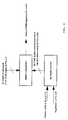
- Fig. 2 shows the internal structure that may be used to realize the final power amplifying block.
- This class-D power amplifying module is described and illustrated in the European patent No. 98830685.8, filed on 13th November, 1998, in the name of the same applicant.
- the circuit does not require the generation of a reference triangular wave or any self-oscillating structures, making it usable also for analog inputs. Different inputs may be selected by a dedicated input configuration network (not shown as in the figure it would be irrelevant in the present context).
- Figures 3 and 4 show respectively the functional block diagram and the operation functioning waveforms of each PCM/PWM converter used in the amplifier scheme of Fig. 1, the signal indications being those of the first of the two converters fed through the P bit (MSB) bus.
- MSB P bit
- both converters are of single ramp type.
- the ramp is generated by a cyclic and resettable up-counter, fed with a clock signal Fclock of a frequency equal to the product of the bit rate of the data transmitted on the respective bus and the square of the number of bit in which the fed data are organized.
- the signal output from each of the two PCM/PWM converters is a PWM signal, whose duty cycle depends on the MSB or LSB input data.
- the pair of PWM signals obtained from the separate conversion of the two portions of bits, respectively MSBdig and LSBdig, are eventually added on the inverting input node (-) of the final power amplifying module, after the LSBdig PWM signal is attenuated, by a factor equivalent to a ratio equivalent to the square of the number S of bits input through the second bus to the second converter.
- the main PWM signal MSBdig generated produced by the first PCM/PWM converter, drives by the output stage determining a switching frequency equal to Fin*K.
- the attenuated PWM signal LSBdig generated by the second converter PCM/PWM drives the output stage with a weight reduced by 1/2 S and thereby it does not affect the switching frequency of the output power stage but modulates the output PWM signal compensating for nonlinearities and attenuating the noise introduced by the quantization of a reduced number P of bits of the main PWM signal MSBdig.
- Fig. 5 An alternative embodiment of the amplifier of the invention is shown in Fig. 5.
- the use of double ramp PCM/PWM converters determines a frequency of their respective PWM output signals halved in respect to the bit rate of the input PCM data.
- Figures 6 and 7 show respectively the functional block diagram of the two PCM/PWM double ramp converters and the relative operation waveforms.
- the indications refer to the first of the two converters, fed through the P bit bus (MSB).
- Fig. 6 shows the feeding of a second clock signal Fup/down with the same multiplied frequency Fin*K of the data input to the converter that synchronizes the ramp inversions.
- the amplifier of the invention may also be realized in the form of a bridge amplifier by using two final power amplifying stages driven in phase opposition rather than in a single ended form.
- Fig. 8 shows the diagram of a bridge version of the amplifier, wherein the required inversion is implemented by inverting the data input to the second final stage of the power amplifier.
- Fig. 9 shows an alternative embodiment of a bridge amplifier of the invention with a phase shift bridge output architecture, which is relatively more complex than that of Fig. 8, though capable of providing for enhanced performances, as described and illustrated in the above cited prior European patent application No. 98830685.8.
- Fig. 10 shows a further embodiment of a bridge amplifier of the invention in which rather than inverting the data fed to the input of one of the pair of final power stages functioning in phase opposition, the inversion is implemented by inverting the up-down command of the respective counters of the second pair of PCM/PWM converters, such to generate triangular reference signals in phase opposition with each other.
- a fourth embodiment of the bridge amplifier of the invention is illustrated in Fig. 11.
- the PWM signals of double frequency compared to the frequency of the main PWM signal relative to the conversion of the least significant bits are summed to the respective main PWM signals produced by the respective PCM/PWM converters fed with the most significant bits on the respective inverting input nodes of the two final power stages.
- Another characteristic of the correction operated by the separate conversion of the least significant bits is a greater freedom because the correction current may be summed, subtracted or may not influence the main drive current signal relative to the conversion of most significant bits.
- An advantage of a bridge embodiment of the amplifier of the invention is that the correction signal does not contain tones at the PWM switching frequency nor at frequencies near the switching frequency. Notably, tones in a ⁇ 20 kHz band centered on the switching frequency are brought back in base band, causing an increase of the distortion and/or of noise.
Abstract

Description
- "Noise shaping and Pulse-Width Modulation for All-Digital Audio Power Amplifiers" by J.M. Goldberg and M.B. Sandler, Journal Audio Eng. Doc., Vol. 39, No. 6, 1991 June. This system described does not use any feedback circuit on the final stage, which to some extent penalizes the performance in terms of distortion and noise rejection. The performance appears to be strictly dependent on the characteristics of the components of the power stage (Fig. 8);
- "All digital Power Amplifier Based on Pulse Width Modulation" by M.S. Pedersen and M. Shajaan, presented during the 96th AES convention (Audio Engineering Society), 26th February, 1st March, 1994, in Amsterdam. According to this design approach there is no feedback circuit. The system appears to be burdened by resorting to a linearized PWM;
- "A Sigma-Delta Power Amplifier for Digital Input Signals" by Klugbauer-Heilmeier presented during the 102nd AES (Audio Engineering Society) convention 22nd-25th March, 1997, in Munich. The article describes a pulse density modulation (PDM) amplifier requiring a high switching frequency besides an antialiasing filter in the feedback path.
Claims (8)
- A digital input PWM power amplifier comprising:an oversampling and noise shaping circuit receiving pulse code modulated (PCM) digital input data organized in words of a first number M of bits at a certain bit rate (Fin) and outputting pulse code modulated digital data organized in words of a smaller number N of bits at a multiple bit rate (Fin*K);a first bus transmitting a first number (P) of most significant bits (MSB) of said N bit words output from said first circuit and a second bus transmitting a second number (S) of least significant bits of said N bit words output from said first circuit;first and second PCM/PWM converters, respectively fed with said first and second number of bits transmitted through said first and said second bus, each converter including a counter driven by a clock signal (Fclock) of frequency equal to the product of the bit rate (Fin*K) of the MSB and LSB bits transmitted on the respective bus and the square of the respective number of bits (P, S) generating reference digital words composed of said respective number of bits (P, S), defining ramps of digital values with a frequency identical to said multiple bit rate (Fin K), and a digital comparator receiving through a first input said reference digital words and through a second input the respective first and second number of bits (MSB, LSB) and outputting a respective PWM signal (MSBdig, LSBdig);the PWM signal (MSBig) output by said first converter, being summed to the so attenuated PWM signal (LSBdig) output by said second converter on the inverting input node (-) of said output power stage.
- The PWM amplifier according to claim 1, characterized in that said first and second PCM/PWM converters are of the single ramp type.
- The PWM amplifier according to claim 1, characterized in that said first and second PCM/PWM converters, are of the double ramp type, said counter being of the up/down type and generating reference digital words composed of said second number (S) of least significant bits in the form of a succession of rising and falling ramps of a halved frequency compared to said multiple bit rate (Fin*k).
- The PWM amplifier according to any of the preceding claims characterized in that is single ended and employs a single output power stage.
- A PWM bridge amplifier according to any of claims 1, 2 and 3, having a pair of identical output power stages functioning in phase opposition in which the inversion of the driving signal to the inverting input of one of the two power stages is realized by inverting the PWM signals output by said pair of PCM/PWM converters.
- A PWM bridge amplifier according to any of the claims 1, 2 and 3, employing a pair of identical output power stages functioning in phase opposition and in which the inversion of the driving signal of one of the two power stages is realized by inverting each of said first and second buses and duplicating said pair of PCM/PWM converters.
- A PWM bridge amplifier according to any of the claims 1, 2 and 3, employing a pair of identical output power stages functioning in phase opposition in which the inversion of the driving signal fed to the inverting input of one of the two power stages is realized by duplicating said pair of PCM/PWM converters, coupling the inputs of the two converters forming said duplicated second pair of PCM/PWM converters to said first and second bus without preventively inverting them but inverting instead the ramp inversion commands (Fup-down) of the two PCM/PWM converters of said duplicated pair.
- The amplifier according to claim 7, characterized in that it also comprises means for inverting the PWM signals output by the PCM/PWM converters of said two pairs of converters that are fed with said least significant bits (LSBdig), second attenuating means (RLSB2+RLSB1-) of said inverted signals and means to respectively sum said inverted and attenuated signals on the inverting input node to the signals produced by the other PCM/PWM converter of the respective pair of converters.
Priority Applications (4)
| Application Number | Priority Date | Filing Date | Title |
|---|---|---|---|
| EP99830073A EP1028524B1 (en) | 1999-02-11 | 1999-02-11 | PWM power amplifier with digital input |
| DE69919500T DE69919500T2 (en) | 1999-02-11 | 1999-02-11 | PWM power amplifier with digital input |
| US09/497,843 US6594309B1 (en) | 1999-02-11 | 2000-02-03 | PWM power amplifier with digital input |
| JP2000034045A JP2000244257A (en) | 1999-02-11 | 2000-02-10 | Pwm power amplifier having digital input |
Applications Claiming Priority (1)
| Application Number | Priority Date | Filing Date | Title |
|---|---|---|---|
| EP99830073A EP1028524B1 (en) | 1999-02-11 | 1999-02-11 | PWM power amplifier with digital input |
Publications (2)
| Publication Number | Publication Date |
|---|---|
| EP1028524A1 true EP1028524A1 (en) | 2000-08-16 |
| EP1028524B1 EP1028524B1 (en) | 2004-08-18 |
Family
ID=8243274
Family Applications (1)
| Application Number | Title | Priority Date | Filing Date |
|---|---|---|---|
| EP99830073A Expired - Lifetime EP1028524B1 (en) | 1999-02-11 | 1999-02-11 | PWM power amplifier with digital input |
Country Status (4)
| Country | Link |
|---|---|
| US (1) | US6594309B1 (en) |
| EP (1) | EP1028524B1 (en) |
| JP (1) | JP2000244257A (en) |
| DE (1) | DE69919500T2 (en) |
Cited By (9)
| Publication number | Priority date | Publication date | Assignee | Title |
|---|---|---|---|---|
| WO2003017469A1 (en) * | 2001-08-17 | 2003-02-27 | Pulsus Technologies | Pulse width modulation type audio amplifier having variable average switching frequency |
| EP1388943A1 (en) * | 2002-08-06 | 2004-02-11 | Lg Electronics Inc. | Multi-channel pulse width modulation apparatus |
| US6724249B1 (en) | 2002-11-07 | 2004-04-20 | Dialog Semiconductor Gmbh | Multi-level class-D amplifier by means of 3 physical levels |
| WO2005018089A1 (en) * | 2003-08-18 | 2005-02-24 | Koninklijke Philips Electronics N. V. | Audio power amplifier |
| KR100538361B1 (en) * | 2002-08-10 | 2005-12-21 | 엘지전자 주식회사 | Apparatus for canceling a noise in multi channel pulse width modulator |
| CN1310427C (en) * | 2004-02-25 | 2007-04-11 | 凌阳科技股份有限公司 | Pulse-width modulation circuit and method |
| KR100906427B1 (en) * | 2002-08-08 | 2009-07-09 | 엘지전자 주식회사 | Apparatus for controlling on/off each channel in multi channel pulse width modulator |
| KR100932501B1 (en) * | 2002-08-06 | 2009-12-17 | 엘지전자 주식회사 | Channel-specific gain regulator in multichannel pulse width modulator |
| KR101006044B1 (en) * | 2001-12-21 | 2011-01-06 | 방 앤드 올루프센 아이스파워 에이/에스 | Attenuation control for digital power converters |
Families Citing this family (30)
| Publication number | Priority date | Publication date | Assignee | Title |
|---|---|---|---|---|
| US7061979B1 (en) * | 2000-05-26 | 2006-06-13 | Ciena Corporation | System and method for determining the data rate of a digital data stream |
| KR100435182B1 (en) * | 2002-02-05 | 2004-06-09 | 주식회사 디지털앤아날로그 | Digital pwm input d class amplifier by pwm negative feedback |
| US7142597B2 (en) * | 2002-09-26 | 2006-11-28 | Freescale Semiconductor, Inc. | Full bridge integral noise shaping for quantization of pulse width modulation signals |
| US20040223545A1 (en) * | 2003-03-04 | 2004-11-11 | Lee Ying Lau | Multi-level pulse width modulation in digital system |
| US20040189502A1 (en) * | 2003-03-04 | 2004-09-30 | Lee Ying Lau | Multi-level pulse width modulation in digital system |
| US7259704B2 (en) | 2003-03-28 | 2007-08-21 | Ess Technology, Inc. | System and method for compensating for error in a sigma delta circuit |
| US7058464B2 (en) * | 2003-07-17 | 2006-06-06 | Ess Technology, Inc. | Device and method for signal processing |
| US7515072B2 (en) | 2003-09-25 | 2009-04-07 | International Rectifier Corporation | Method and apparatus for converting PCM to PWM |
| US7190224B2 (en) * | 2003-11-06 | 2007-03-13 | Marvell World Trade Ltd. | Class D amplifier |
| US7130346B2 (en) * | 2004-05-14 | 2006-10-31 | Freescale Semiconductor, Inc. | Method and apparatus having a digital PWM signal generator with integral noise shaping |
| KR100810322B1 (en) * | 2004-10-29 | 2008-03-07 | 삼성전자주식회사 | Apparatus and method for high efficiency power amplifier for mobile communication system |
| US7570693B2 (en) * | 2005-09-26 | 2009-08-04 | Ess Technology, Inc. | Low noise digital to pulse width modulated converter with audio applications |
| US7116257B1 (en) | 2005-09-26 | 2006-10-03 | Ess Technology, Inc. | Low noise digital to analog converter with audio applications |
| US7138935B1 (en) | 2005-09-26 | 2006-11-21 | Ess Technology, Inc. | Low noise digital to signal interval converter with audio applications |
| US7492219B1 (en) | 2006-08-10 | 2009-02-17 | Marvell International Ltd. | Power efficient amplifier |
| US7724161B1 (en) | 2006-12-12 | 2010-05-25 | Marvell International Ltd. | Truncation for three-level digital amplifier |
| JP4793294B2 (en) * | 2007-03-16 | 2011-10-12 | ヤマハ株式会社 | Digital input class D amplifier |
| WO2009043017A1 (en) * | 2007-09-27 | 2009-04-02 | Nanoamp Solutions, Inc. (Cayman) | A transmitter for multiple standards |
| US7701307B2 (en) * | 2008-04-01 | 2010-04-20 | Silicon Laboratories, Inc. | System and method of changing a PWM power spectrum |
| US7791521B2 (en) * | 2008-04-01 | 2010-09-07 | Silicon Laboratories, Inc. | System and method of changing a PWM power spectrum |
| US7598895B1 (en) * | 2008-04-01 | 2009-10-06 | Silicon Laboratories, Inc. | System and method of altering a PWM carrier power spectrum |
| EP2128990B1 (en) * | 2008-05-28 | 2013-03-06 | Siemens Aktiengesellschaft | A method and circuit for converting an N-bit digital value into an analog value |
| US8130128B2 (en) | 2010-03-30 | 2012-03-06 | Silicon Laboratores Inc. | System and method for generating shaped noise |
| US8217820B2 (en) | 2010-11-04 | 2012-07-10 | Maxim Integrated Products, Inc. | Using multi-level pulse width modulated signal for real time noise cancellation |
| CN103460598A (en) | 2011-03-28 | 2013-12-18 | 松下电器产业株式会社 | Amplifier and audio device provided with amplifier |
| US8570202B2 (en) * | 2012-02-03 | 2013-10-29 | Sigear Europe Sarl | Digital-to-analog converter implementing hybrid conversion architecture |
| JP2013172293A (en) * | 2012-02-21 | 2013-09-02 | Cri Middleware Co Ltd | Analog signal generation method, analog signal generation apparatus, and program |
| US9705485B1 (en) * | 2015-07-13 | 2017-07-11 | Marvell Israel (M.I.S.L) Ltd | High-resolution current and method for generating a current |
| EP3211800B1 (en) | 2016-02-25 | 2019-10-16 | Huawei Technologies Co., Ltd. | Signal processing arrangement for a transmitter |
| US10848176B1 (en) * | 2019-10-01 | 2020-11-24 | Raytheon Company | Digital delta-sigma modulator with non-recursive computation of residues |
Citations (7)
| Publication number | Priority date | Publication date | Assignee | Title |
|---|---|---|---|---|
| EP0212990A2 (en) * | 1985-08-29 | 1987-03-04 | Canon Kabushiki Kaisha | Image processing apparatus |
| US4673887A (en) * | 1986-01-03 | 1987-06-16 | Honeywell Inc. | Digital driver for fixed power amplifier |
| US4683439A (en) * | 1986-01-09 | 1987-07-28 | Honeywell Inc. | Digitally driven switching power amplifier system |
| EP0383689A2 (en) * | 1989-02-14 | 1990-08-22 | Sony Corporation | Digital-to-analog converter |
| EP0457496A2 (en) * | 1990-05-16 | 1991-11-21 | Sony Corporation | Digital-to-analogue converter |
| EP0597687A1 (en) * | 1992-11-12 | 1994-05-18 | NCR International, Inc. | Method and apparatus for generating sound in a digital computer |
| US5406284A (en) * | 1992-12-31 | 1995-04-11 | Monolith Technologies Corporation | Methods and apparatus for the quantization and analog conversion of digital signals |
Family Cites Families (3)
| Publication number | Priority date | Publication date | Assignee | Title |
|---|---|---|---|---|
| CA1289666C (en) * | 1983-10-25 | 1991-09-24 | Masashi Takeda | Digital-to-analog converting system |
| US5959501A (en) * | 1998-01-14 | 1999-09-28 | Harris Corporation | Class D amplifier with scaled clock and related methods |
| US6014055A (en) * | 1998-02-06 | 2000-01-11 | Intersil Corporation | Class D amplifier with reduced clock requirement and related methods |
-
1999
- 1999-02-11 EP EP99830073A patent/EP1028524B1/en not_active Expired - Lifetime
- 1999-02-11 DE DE69919500T patent/DE69919500T2/en not_active Expired - Fee Related
-
2000
- 2000-02-03 US US09/497,843 patent/US6594309B1/en not_active Expired - Fee Related
- 2000-02-10 JP JP2000034045A patent/JP2000244257A/en active Pending
Patent Citations (7)
| Publication number | Priority date | Publication date | Assignee | Title |
|---|---|---|---|---|
| EP0212990A2 (en) * | 1985-08-29 | 1987-03-04 | Canon Kabushiki Kaisha | Image processing apparatus |
| US4673887A (en) * | 1986-01-03 | 1987-06-16 | Honeywell Inc. | Digital driver for fixed power amplifier |
| US4683439A (en) * | 1986-01-09 | 1987-07-28 | Honeywell Inc. | Digitally driven switching power amplifier system |
| EP0383689A2 (en) * | 1989-02-14 | 1990-08-22 | Sony Corporation | Digital-to-analog converter |
| EP0457496A2 (en) * | 1990-05-16 | 1991-11-21 | Sony Corporation | Digital-to-analogue converter |
| EP0597687A1 (en) * | 1992-11-12 | 1994-05-18 | NCR International, Inc. | Method and apparatus for generating sound in a digital computer |
| US5406284A (en) * | 1992-12-31 | 1995-04-11 | Monolith Technologies Corporation | Methods and apparatus for the quantization and analog conversion of digital signals |
Cited By (11)
| Publication number | Priority date | Publication date | Assignee | Title |
|---|---|---|---|---|
| WO2003017469A1 (en) * | 2001-08-17 | 2003-02-27 | Pulsus Technologies | Pulse width modulation type audio amplifier having variable average switching frequency |
| KR101006044B1 (en) * | 2001-12-21 | 2011-01-06 | 방 앤드 올루프센 아이스파워 에이/에스 | Attenuation control for digital power converters |
| EP1388943A1 (en) * | 2002-08-06 | 2004-02-11 | Lg Electronics Inc. | Multi-channel pulse width modulation apparatus |
| US7580532B2 (en) | 2002-08-06 | 2009-08-25 | Lg Electronics Inc. | Multi-channel pulse width modulation apparatus |
| KR100932501B1 (en) * | 2002-08-06 | 2009-12-17 | 엘지전자 주식회사 | Channel-specific gain regulator in multichannel pulse width modulator |
| KR100906427B1 (en) * | 2002-08-08 | 2009-07-09 | 엘지전자 주식회사 | Apparatus for controlling on/off each channel in multi channel pulse width modulator |
| KR100538361B1 (en) * | 2002-08-10 | 2005-12-21 | 엘지전자 주식회사 | Apparatus for canceling a noise in multi channel pulse width modulator |
| US6724249B1 (en) | 2002-11-07 | 2004-04-20 | Dialog Semiconductor Gmbh | Multi-level class-D amplifier by means of 3 physical levels |
| EP1418667A1 (en) * | 2002-11-07 | 2004-05-12 | Dialog Semiconductor GmbH | Multi-level class-D amplifier by means of 3 physical levels |
| WO2005018089A1 (en) * | 2003-08-18 | 2005-02-24 | Koninklijke Philips Electronics N. V. | Audio power amplifier |
| CN1310427C (en) * | 2004-02-25 | 2007-04-11 | 凌阳科技股份有限公司 | Pulse-width modulation circuit and method |
Also Published As
| Publication number | Publication date |
|---|---|
| EP1028524B1 (en) | 2004-08-18 |
| DE69919500T2 (en) | 2005-09-08 |
| JP2000244257A (en) | 2000-09-08 |
| DE69919500D1 (en) | 2004-09-23 |
| US6594309B1 (en) | 2003-07-15 |
Similar Documents
| Publication | Publication Date | Title |
|---|---|---|
| EP1028524B1 (en) | PWM power amplifier with digital input | |
| US7612608B2 (en) | Sigma-delta based Class D audio or servo amplifier with load noise shaping | |
| EP1653604B1 (en) | Switching power amplifier and method for amplifying a digital input signal | |
| US7498876B2 (en) | Amplifier having half-wave tracking power rails | |
| US6693571B2 (en) | Modulation of a digital input signal using a digital signal modulator and signal splitting | |
| US7605653B2 (en) | Sigma-delta based class D audio power amplifier with high power efficiency | |
| US7557744B2 (en) | PWM driver and class D amplifier using same | |
| US7482865B2 (en) | Systems and methods for correcting errors resulting from component mismatch in a feedback path | |
| EP1178388B1 (en) | PCM/PWM converter with PWM power amplifier | |
| US20060072657A1 (en) | Pulse width-modulated noise shaper | |
| US6307431B1 (en) | PWM bridge amplifier with input network configurable for analog or digital input not needing a triangular wave generator | |
| US6762704B1 (en) | Modulation of a digital input signal using multiple digital signal modulators | |
| US6724249B1 (en) | Multi-level class-D amplifier by means of 3 physical levels | |
| CN101183855B (en) | D-type amplifier | |
| Hiorns et al. | A PWM DAC for digital audio power conversion: from theory to performance | |
| US8314657B2 (en) | D-class amplifier | |
| JPH0563457A (en) | Delta/sigma modulation amplifier | |
| Bresch et al. | TMS320C67-based design of a digital audio power amplifier introducing novel feedback strategy | |
| JP4061764B2 (en) | D / A converter | |
| US7706438B1 (en) | Circuits and methods for reducing noise and distortion in pulse width modulation systems | |
| JPH05152867A (en) | Class d amplifier | |
| JP2023102002A (en) | Analog modulator and switching amplifier using analog modulator | |
| Yu et al. | An FPGA-based digital class-D amplifier with power supply error correction | |
| JPH06209913A (en) | Magnetic resonance imaging device | |
| JPS5937731A (en) | Digital-analog converter |
Legal Events
| Date | Code | Title | Description |
|---|---|---|---|
| PUAI | Public reference made under article 153(3) epc to a published international application that has entered the european phase |
Free format text: ORIGINAL CODE: 0009012 |
|
| AK | Designated contracting states |
Kind code of ref document: A1 Designated state(s): DE FR GB IT |
|
| AX | Request for extension of the european patent |
Free format text: AL;LT;LV;MK;RO;SI |
|
| 17P | Request for examination filed |
Effective date: 20000804 |
|
| AKX | Designation fees paid |
Free format text: DE FR GB IT |
|
| GRAP | Despatch of communication of intention to grant a patent |
Free format text: ORIGINAL CODE: EPIDOSNIGR1 |
|
| GRAS | Grant fee paid |
Free format text: ORIGINAL CODE: EPIDOSNIGR3 |
|
| GRAA | (expected) grant |
Free format text: ORIGINAL CODE: 0009210 |
|
| AK | Designated contracting states |
Kind code of ref document: B1 Designated state(s): DE FR GB IT |
|
| REG | Reference to a national code |
Ref country code: GB Ref legal event code: FG4D |
|
| REF | Corresponds to: |
Ref document number: 69919500 Country of ref document: DE Date of ref document: 20040923 Kind code of ref document: P |
|
| PG25 | Lapsed in a contracting state [announced via postgrant information from national office to epo] |
Ref country code: GB Free format text: LAPSE BECAUSE OF NON-PAYMENT OF DUE FEES Effective date: 20050211 |
|
| PLBE | No opposition filed within time limit |
Free format text: ORIGINAL CODE: 0009261 |
|
| STAA | Information on the status of an ep patent application or granted ep patent |
Free format text: STATUS: NO OPPOSITION FILED WITHIN TIME LIMIT |
|
| ET | Fr: translation filed | ||
| 26N | No opposition filed |
Effective date: 20050519 |
|
| GBPC | Gb: european patent ceased through non-payment of renewal fee |
Effective date: 20050211 |
|
| PGFP | Annual fee paid to national office [announced via postgrant information from national office to epo] |
Ref country code: DE Payment date: 20070131 Year of fee payment: 9 |
|
| PGFP | Annual fee paid to national office [announced via postgrant information from national office to epo] |
Ref country code: IT Payment date: 20070607 Year of fee payment: 9 |
|
| PGFP | Annual fee paid to national office [announced via postgrant information from national office to epo] |
Ref country code: FR Payment date: 20070227 Year of fee payment: 9 |
|
| REG | Reference to a national code |
Ref country code: FR Ref legal event code: ST Effective date: 20081031 |
|
| PG25 | Lapsed in a contracting state [announced via postgrant information from national office to epo] |
Ref country code: DE Free format text: LAPSE BECAUSE OF NON-PAYMENT OF DUE FEES Effective date: 20080902 |
|
| PG25 | Lapsed in a contracting state [announced via postgrant information from national office to epo] |
Ref country code: FR Free format text: LAPSE BECAUSE OF NON-PAYMENT OF DUE FEES Effective date: 20080229 |
|
| PG25 | Lapsed in a contracting state [announced via postgrant information from national office to epo] |
Ref country code: IT Free format text: LAPSE BECAUSE OF NON-PAYMENT OF DUE FEES Effective date: 20080211 |