EP1030454A2 - Bit interleave circuit and bit deinterleave circuit - Google Patents
Bit interleave circuit and bit deinterleave circuit Download PDFInfo
- Publication number
- EP1030454A2 EP1030454A2 EP00100163A EP00100163A EP1030454A2 EP 1030454 A2 EP1030454 A2 EP 1030454A2 EP 00100163 A EP00100163 A EP 00100163A EP 00100163 A EP00100163 A EP 00100163A EP 1030454 A2 EP1030454 A2 EP 1030454A2
- Authority
- EP
- European Patent Office
- Prior art keywords
- bit
- counter
- signal
- address
- circuit
- Prior art date
- Legal status (The legal status is an assumption and is not a legal conclusion. Google has not performed a legal analysis and makes no representation as to the accuracy of the status listed.)
- Withdrawn
Links
Images


Classifications
-
- H—ELECTRICITY
- H03—ELECTRONIC CIRCUITRY
- H03M—CODING; DECODING; CODE CONVERSION IN GENERAL
- H03M13/00—Coding, decoding or code conversion, for error detection or error correction; Coding theory basic assumptions; Coding bounds; Error probability evaluation methods; Channel models; Simulation or testing of codes
- H03M13/27—Coding, decoding or code conversion, for error detection or error correction; Coding theory basic assumptions; Coding bounds; Error probability evaluation methods; Channel models; Simulation or testing of codes using interleaving techniques
- H03M13/276—Interleaving address generation
- H03M13/2764—Circuits therefore
-
- H—ELECTRICITY
- H03—ELECTRONIC CIRCUITRY
- H03M—CODING; DECODING; CODE CONVERSION IN GENERAL
- H03M13/00—Coding, decoding or code conversion, for error detection or error correction; Coding theory basic assumptions; Coding bounds; Error probability evaluation methods; Channel models; Simulation or testing of codes
- H03M13/27—Coding, decoding or code conversion, for error detection or error correction; Coding theory basic assumptions; Coding bounds; Error probability evaluation methods; Channel models; Simulation or testing of codes using interleaving techniques
- H03M13/2703—Coding, decoding or code conversion, for error detection or error correction; Coding theory basic assumptions; Coding bounds; Error probability evaluation methods; Channel models; Simulation or testing of codes using interleaving techniques the interleaver involving at least two directions
Definitions
- the present invention relates to a bit interleave circuit and a bit deinterleave circuit which are used in a mobile communication system or a mobile broadcasting system.
- Shadowing is a phenomenon in which an electric wave is blocked by a building or the like.
- fading is a phenomenon in which interference between multipath delayed waves occurs.
- FEC Forward Error Correction
- a bit interleave circuit and a bit deinterleave circuit are employed on the transmitter and receiver sides, respectively in many cases.
- a random-access memory with a 2-plane configuration is employed so as to allow a series of output codes generated by an error correction encoder to be transmitted by changing the order of the codes in accordance with a proper rule.
- the received codes are rearranged in the reverse order to reproduce the original series of codes which is then supplied to an error correction decoder. In this way, burst errors generated along the radio transmission path can be randomized so that the deterioration of the ability to correct an error is reduced.
- Fig. 22 is a diagram showing the configuration of the conventional bit interleave circuit
- Fig. 23 is a diagram showing the configuration of the conventional bit deinterleave circuit
- Fig. 24 is an explanatory diagram used for describing the operations of the bit interleave and bit deinterleave circuits shown in Figs. 22 and 23 respectively for an interleave block of 4 ⁇ 4 bits.
- bit interleave circuit 54 As shown in Fig. 24, information coded by an FEC encoder 50 by adopting a convolution encoding technique or the like is converted into serial data by a P/S converter 52 before being fed to the bit interleave circuit 54 shown in Fig. 22.
- a horizontal-direction counter 6 employed in a write-address counter 2 counts the number of clocks synchronized with an input signal repeatedly from 0 to 3, outputting the clock count to an address terminal of either a RAM 16#0 or a RAM 16#1 by way of a selector 14#0 or 14#1, respectively as a lower-order address.
- a vertical-direction counter 4 also employed in the write-address counter 2 counts the number of clock periods repeatedly from 0 to 3, outputting the clock-period count to the address terminal of either the RAM 16#0 or the RAM 16#1 by way of the selector 14#0 or 14#1, respectively as an upper-order address.
- a clock period the counting period of the horizontal-direction counter 6 is meant.
- a RAM plane switching control signal controls the RAMs 16#0 and 16#1 so that their write-in and read-out operations are mutually exclusive. To be more specific, when a read operation is carried out on one of the RAMs 16#0 or 16#1, a write operation is carried out on the other.
- a gate circuit 18#0 supplies a RAM write timing signal to a write enable terminal WE of the RAM 16#0 in accordance with the RAM plane switching control signal.
- a gate circuit 18#1 supplies a RAM write timing signal to a write enable terminal WE of the RAM 16#1 in accordance with the RAM plane switching control signal.
- a gate circuit 20#0 receives a serial transmission signal (0 to F), outputting the signal to a terminal data #0 of the RAM 16#0 in accordance with the RAM plane switching control signal.
- a gate circuit 20#1 receives a serial transmission signal (0 to F), outputting the signal to a terminal data #0 of the RAM 16#1 in accordance with the RAM plane switching control signal.
- the reference numerals 0 to F are hexadecimal numbers representing the contents of the encoded list.
- a vertical-direction counter 12 employed in a read-address counter 8 repeatedly counts the number of clocks synchronized with an input signal from 0 to 3, outputting the clock count to the selector either 14#0 or 14#1, respectively as an upper-order address.
- a horizontal-direction counter 10 also employed in the read-address counter 8 counts the number of clock periods repeatedly from 0 to 3, outputting the clock-period count to the address terminal of either the RAM 16#0 or the RAM 16#1 by way of the selector 14#0 or 14#1, respectively as a lower-order address.
- the counting period of the vertical-direction counter 12 is meant.
- Either of the RAMs 16#0 and the 16#1 outputs an encoded list from a location indicated by an address supplied to the address terminal thereof to a transmission system by way of a selector 22. In this way, the signal to be transmitted is interleaved in the order of 0, 4, 8, C, 1, 5, 9 and so on.
- a vertical-direction counter 34 employed in a write-address counter 30 counts the number of clocks synchronized with an input signal, repeatedly from 0 to 3, outputting the clock count to the address terminal of either a RAM 42#0 or a RAM 42#1 by way of a selector 40#0 or 40#1, respectively as an upper-order address.
- a horizontal-direction counter 32 also employed in the write-address counter 30 counts the number of clock periods repeatedly from 0 to 3, outputting the clock-period count to the address terminal of either the RAM 42#0 or the RAM 42#1 by way of the selector 40#0 or 40#1, respectively as a lower-order address.
- the counting period of the vertical-direction counter 34 is meant.
- Data supplied to the terminal data #0 is written into a location in the RAM 42#0 or 42#1 indicated by the address signal supplied to the address terminal.
- a signal i received in the order of 0, 4, 8, C, 1 and so on is written at an address i where i is the order number of the encoded list prior to the interleave process.
- a horizontal-direction counter 39 employed in a read-address counter 36 repeatedly counts the number of clocks synchronized with an input signal from 0 to 3, outputting the clock count to the address terminal of either the RAM 42#0 or the RAM 42#1 by way of the selector 40#0 or 40#1, respectively as a lower-order address.
- a vertical-direction counter 38 also employed in the read-address counter 36 counts the number of clock periods repeatedly from 0 to 3, outputting the clock-period count to the address terminal of either the RAM 42#0 or the RAM 42#1 by way of the selector 40#0 or 40#1, respectively as an upper-order address.
- the counting period of the horizontal-direction counter 39 is meant.
- Either one of the RAMs 42#0 or the 42#1 outputs an encoded list from a location indicated by an address signal supplied to the address terminal by way of a selector 48. In this way, the received signal is correctly deinterleaved to the preinterleave order 0, 1, 2 and so on.
- the conventional bit interleave circuit and the conventional bit deinterleave circuit described above since write and read operations are simply carried out in the horizontal and vertical directions as shown in Figs. 22 to 24, if consecutive errors occur in the last bit of an interleave block and the first bit of the following interleave block, the consecutive errors will remain even after the bit deinterleave process, raising a problem that randomization of errors after the bit deinterleave process is not always sufficient.
- the parallel output of the FEC encoder is converted into serial data prior to an bit interleave process in the conventional mobile communication/broadcasting system.
- received serial data is converted into parallel data after a bit deinterleave process. In this way, it is possible to prevent input bits from becoming erroneous at the same time.
- Fig. 24 is a diagram showing examples of operations carried out at a coding rate of 1/2. In this case, it is necessary to write and read data into and from a RAM at a clock rate twice as much as the bit rate of the information. In consequence, among other problems, there is raised an issue that not only is it difficult to implement a bit interleave circuit capable of operating at a high speed, but the amount of power consumption also increases as well.
- a bit deinterleave circuit bit deinterleaving a signal
- the bit deinterleave circuit comprising: measurement means for measuring the reception level of each bit in a received signal completing a bit interleave process; command-signal generating means for outputting a command signal to indicate whether computation in error correction is to be inhibited or permitted for said bit on the basis of said reception level of each bit measured by said measurement means and a threshold value; first deinterleave means for deinterleaving said received signal completing a bit interleave process; and second deinterleave means for rearranging said command signals so as to output command signals according to a signal output by said first deinterleave means.
- a bit interleave circuit bit interleaving a signal comprising:random-access memory allowing operations based on an address signal to write and read data; first counter for carrying out a counting operation synchronized with an input encoded list and outputting a lower-order address of said address signal; second counter for carrying out a counting operation synchronized with counting periods of said first counter and outputting an upper-order address of said address signal; third counter for carrying out a counting operation synchronized with said input encoded list and outputting an upper-order address of said address signal; fourth counter for carrying out a counting operation synchronized with counting periods of said third counter and outputting a lower-order address of said address signal; and inverter circuit for inverting the most significant bit of either said second counter or said third counter.
- a bit deinterleave circuit comprises: a measurement means 62 for measuring the reception level of each bit in a received signal completing a bit interleave process; a command-signal generating means 64 for outputting a command signal to indicate whether computation in error correction is to be inhibited or permitted for each bit on the basis of the reception level of the bit measured by the measurement means 62 and a threshold value; a first deinterleave means 66 for deinterleaving the received signal completing a bit interleave process; and a second deinterleave means 68 for rearranging command signals so as to output the command signals according to a signal output by the first deinterleave means 66.
- the reception level measured by the measurement means 62 is information on the amplitude of each bit in a received signal completing a bit interleave process. This is because fading or shadowing attenuates the reception level and the reception-level attenuation makes the reception characteristic deteriorate.
- the command-signal generating means 64 compares the reception level of each bit measured by the measurement means 62 with a threshold value. For example, if the reception level of a bit is found lower than the threshold value, a command signal is issued to request that computation be inhibited as shown by an X mark in the figure.
- a command signal is issued to indicate that computation is allowed as shown by an ⁇ mark in the figure. Assume that the reception level of a bit is lower than the threshold value during the period t0 to t1. In this case, a command signal is issued to request that computation be inhibited during this period.
- the first deinterleave means 66 deinterleaves the received signal completing a bit interleave process by rearranging bits in the signal.
- the second deinterleave means 68 rearranges command signals to output the command signals according to bits of a signal output by the first deinterleave means 66.
- An FEC decoder 69 receives bits of the received signal completing the bit deinterleave process and the command signals according to the bits. If a command signal for a bit indicates that computation is inhibited, a decoding process is carried out by excluding the bit from decoding computation. In this way, a BER characteristic can be prevented from deteriorating.
- Fig. 2 is a diagram showing a radio set including a bit interleave circuit and a bit deinterleave circuit which are implemented by a first embodiment of the present invention.
- the radio set is a mobile station or a base station used in a mobile communication system or the like.
- the radio set comprises an FEC encoder 70, an P/S converter 71, a bit interleave circuit 72, a modulator 74, an RF unit 76, antennas 78 and 80, an RF unit 82, a demodulator 84, an A/D converter 85, a bit deinterleave circuit 86, an S/P converter 87 and an FEC decoder 88.
- the FEC encoder 70 carries out an encoding process at a fixed encoding rate such as the convolution encoding process on incoming information to generate an encoded list of k bits.
- the P/S converter 71 converts the k-bit parallel data into serial data.
- the bit interleave circuit 72 carries out a bit interleave process on encoded serial data in a configuration like the one shown in Fig. 22.
- the modulator 74 modulates a signal completing the bit interleave process by adopting a predetermined modulation method such as the BPSK or QPSK.
- the RF unit 76 transforms frequencies of the modulated signal into a fixed frequency band and amplifies the signal.
- the antenna 78 transmits a transmission signal.
- the antenna 80 receives a radio signal.
- the RF unit 82 extracts a signal in a fixed frequency band and carries out processing such as amplification on the extracted signal.
- the demodulator 84 measures the level of the received signal to output an RSSI (Received Signal Strength Indicator).
- RSSI Receiveived Signal Strength Indicator
- the demodulator 84 controls the amplitude of the received signal by using an AGC circuit and demodulates the received signal which was modulated by the BPSK or QPSK method, outputting a demodulated signal including amplitude information.
- the demodulator 84 generates a demodulated signal including amplitude information in order to increase the error correction capability of the FEC decoder 88.
- the A/D converter 85 converts the demodulated signal into a digital signal comprising a fixed number of quantization bits. Typically, the number of quantization bits is 3 with the code bit of the most significant code bit being an encoded bit.
- Fig. 3 is a diagram showing the configuration of the bit deinterleave circuit 86 shown in Fig. 2. Components of the bit deinterleave circuit substantially identical with those shown Fig. 23 are denoted by the same reference numerals as the latter. As shown in Fig.
- the bit deinterleave circuit 86 comprises a control circuit 90, a delay circuit 92, a computation-inhibit-signal generating circuit 94, a write address counter 30, a read address counter 36, selectors 40#0 and 40#1, RAMs 42#0 and 42#1, gate circuits 44#0, 44#1, 46#0 and 46#1, a selector 48, a write address counter 96, a read address counter 102, selectors 108#0 and 108#1, RAMs 110#0 and 110#1, gate circuits 112#0, 112#1, 114#0 and 114#1 and a selector 116.
- the RAMs 42#0 and 42#1 each have a width of 1 bit, and as many such RAMs as bits output by the A/D converter 85 are provided.
- the control circuit 90 generates a clock signal synchronized with a received signal.
- the control circuit 90 also generates a RAM plane switching control signal and a RAM write timing signal for each interleave block of n ⁇ m bits in synchronization with the clock signal where the symbol n is the number of bits in the horizontal direction in the block whereas the symbol m is the number of bits in the vertical direction in the block.
- the delay circuit 92 is typically implemented by a shift register which operates on the basis of a clock signal synchronized with a received signal.
- the delay circuit 92 delays the received signal completing a bit interleave process by a predetermined delay time equal in length to a period between reception of bits of the received signal and generation of command signals by the computation-inhibit-signal generating circuit 94 to indicate that computation be inhibited or allowed for the bits.
- Fig. 4 is a block diagram showing the computation-inhibit-signal generating circuit 94 employed in the bit deinterleave circuit 86 shown in Fig. 3.
- the computation-inhibit-signal generating circuit 94 comprises a mobile averaging circuit 122, a weight providing circuit 124 and a comparator 126.
- the mobile averaging circuit 122 detects the envelop of an analog signal output by the demodulator 84 and measures the level of the received signal. To be more specific, the mobile averaging circuit 122 measures the reception level of each bit in the received signal and computes an average of reception levels of bits in the received signal within a predetermined range preceding and succeeding the bit. Such an average is referred to hereafter as a mobile average.
- a mobile average is found in order to suppress an effect of noise generated by the radio set. This is because fading or shadowing attenuates the reception level and the reception-level attenuation gives rise to a continuous burst error.
- the weight providing circuit 124 provides weights to reception levels of bits, which were subjected to the mobile-averaging process.
- the weights are found from the RSSI signal or an AGC control voltage output by the demodulator 84.
- the reception levels of the bits are multiplied by the RSSI signal or the AGC control voltage.
- Weights are provided to the reception levels because of the following reason. Since the AGC circuit employed in the demodulator 84 adjusts the level of the received signal, from only the level of a signal output by the demodulator 84, it is impossible to determine the level which the received signal had at the time the received signal arrived the antenna 80. It is thus necessary to return the level of the received signal to that of the received signal which had at the time the received signal arrived at the antenna 80.
- the comparator 126 compares the level of the received signal output by the weight providing circuit 124 with a threshold value (or a reference voltage). If the level of the received signal output by the weight providing circuit 124 exceeds the threshold value, the comparator 126 outputs a command signal set typically at a low level indicating that computation is allowed. If the level of the received signal output by the weight providing circuit 124 is equal to or lower than the threshold value, on the other hand, the comparator 126 outputs a command signal raised typically to a high level indicating that computation is inhibited. If the comparator 126 outputs a command signal indicating that computation is inhibited for a received signal, the FEC decoder 88 inhibits error-correction computation for the received signal with which the command signal is associated.
- a threshold value or a reference voltage
- the write address counter 96 includes a horizontal-direction address counter 98 and a vertical-direction address counter 100.
- the read address counter 102 includes a horizontal-direction counter 106 and a vertical-direction counter 104.
- the operation of this deinterleaver is substantially the same as that of the write address counter 30, the read address counter 36, the selectors 40#0 and 40#1, the RAMs 42#0 and 42#1, the gate circuits 44#0, 44#1, 46#0 and 46#1 and the selector 48.
- the write address counter 96, the read address counter 102, the selectors 108#0 and 108#1 as well as the gate circuits 112#0 and 112#1 can be shared with the deinterleaver of the received signal.
- the operation of the radio set shown in Fig. 2 is explained as follows. Assume that the antenna 80 shown in Fig. 2 receives a modulated signal which was processed by using the same encoding system as the FEC encoder 70, the same bit interleave system as the bit interleave circuit 72 and the same modulation system as the modulator 74. Examples of the encoding system, the bit interleave system and the modulation system are the convolution encoding technique, the 4 ⁇ 4 interleave blocking technique and the BPSK modulation method, respectively.
- the RF unit 82 extracts a signal of a fixed frequency band from the signal received by the antenna 80.
- the demodulator 84 finds an RSSI signal from the received signal and then, after executing AGC control, demodulates the received signal, which was modulated by using typically the BPSK method, into a signal including amplitude information. The modulated signal is then supplied to the A/D converter 85. On the other hand, the RSSI signal and the AGC control voltage are supplied to the bit deinterleave circuit 86.
- the A/D converter 85 converts the modulated signal received thereby into a digital signal with a fixed number of quantization bits.
- the coded bits of the quantization bits are encoded bits completing a bit interleave process and the remaining bits represent amplitude information.
- Fig. 5 is an explanatory diagram used for describing the operation of the bit deinterleave circuit shown in Fig. 3.
- the control circuit 90 generates a clock signal synchronized with a received signal.
- the control circuit 90 also generates a RAM plane switching control signal and a RAM write timing signal each time a bit interleave block of typically 4 ⁇ 4 bits is received.
- the delay circuit 92 delays the received signal by a fixed period of time in order to synchronize the bits of the received signal with command signals each indicating whether computation is inhibited or permitted.
- the mobile averaging circuit 122 shown in Fig. 4 measures the level of the amplitude of the received signal by detecting typically the envelop of the received signal. The mobile averaging circuit 122 then finds an average of the levels of the received signal in a predetermined range including bits of the received signal, supplying the average to the weight providing circuit 124.
- the weight providing circuit 124 provides weights to a signal output by the mobile averaging circuit 122. The weights are based on the RSSI signal and the AGC control voltage. For example, the signal output by the mobile averaging circuit 122 is multiplied by the RSSI signal and the AGC control voltage. The weighted signal is then supplied to the comparator 126.
- the comparator 126 compares the level of the received signal output by the weight providing circuit 124 with a threshold value (or a reference voltage). If the level of the received signal output by the weight providing circuit 124 exceeds the threshold value, the comparator 126 outputs a computation-permit command signal set typically at a low level indicating that computation is allowed. If the level of the received signal output by the weight providing circuit 124 is equal to or lower than the threshold value, on the other hand, the comparator 126 outputs a computation-inhibit command signal raised typically to a high level indicating that computation is inhibited. The comparator 126 outputs the command signal to the gate circuits 114#0 and 114#1 shown in Fig. 3. Fig.
- FIG. 6 is a diagram showing the computation-inhibit command signal output by the comparator 126.
- the computation-inhibit command signal is active, being typically raised to a high level.
- the computation-permit command signal is active, being typically set a low level.
- the write address counter 30, the selectors 40#0 and 40#1 as well as the gate circuits 44#0, 44#1, 46#0 and 46#1 cause one interleave block (0, 4, 8, C and so on) to be written into either the RAM 42#0 or 42#1 at addresses (0, 4, 8, C and so on), respectively as shown in Fig. 5.
- the write address counter 96, the selectors 108#0 and 108#1 as well as the gate circuits 112#0, 112#1, 114#0 and 114#1 cause command signals ( ⁇ , X, X, X, ⁇ and so on) for the 1-block bits (0, 4, 8, C and so on) to be written into either the RAM 110#0 or 110#1 at the same addresses as the block bits have been written as shown in Fig. 5.
- the read address counter 36 as well as the selectors 40#0 and 40#1 cause 1-block bits (0, 1, 2, 3, 4 and so on) to be read out from either the RAM 42#0 or the RAM 42#1 and deinterleaved before being supplied to the S/P converter 87 by way of the selector 48 as shown in Fig. 5.
- the read address counter 102 as well as the selectors 108#0 and 108#1 cause command signals ( ⁇ , ⁇ , ⁇ , ⁇ , X and so on) for the 1-block bits (0, 1, 2, 3, 4 and so on) to be read out from either the RAM 110#0 or the RAM 110#1 before being supplied to the S/P converter 87 by way of the selector 116 as shown in Fig. 5.
- the S/P converter 87 converts each of deinterleaver outputs (0, 1, 2, 3, 4 and so on) of the received signal and deinterleaver outputs ( ⁇ , ⁇ , ⁇ , ⁇ , X and so on) of the command signals into k-bit parallel data which is then output to the FEC decoder 88.
- the FEC decoder 88 receives the parallel data from the S/P converter 87, decoding the data by adoption of typically the viterbi decoding technique.
- an interleaver output is set at a value having no effect on a judgment if the computation-inhibit command signal for the interleaver output is active. In this way, error computation for an erroneous code caused by fading, shadowing or the like is inhibited. As a result, deterioration of the BER characteristic after the error correction can be suppressed.
- Fig. 7 is an explanatory diagram showing effects of the bit deinterleave circuit shown in Fig. 3.
- the horizontal axis of Fig. 7 represents a ratio Es/N o [dB] where the symbol Es is an encoding energy per bit and the symbol N o is an energy per 1Hz of noise.
- the vertical axis represents the BER.
- the figure shows curves for cases with and without the computation-inhibit command signal.
- the encoding rate R 1/2
- the interleave block length 32 ⁇ 256 bits
- the shadowing length (a segment of computation inhibition due to shadowing) 2,736 bits
- the depth of the reception level caused by shadowing -20 dB.
- Fig. 8 is a diagram showing the configuration of a bit interleave circuit implemented by a second embodiment of the present invention. Components of the second embodiment identical with those shown in Fig. 22 are denoted by the same reference numerals as the latter.
- the bit interleave circuit implemented by the second embodiment is different from the conventional bit interleave circuit in that, in the case of the former, a post-interleave distance between two adjacent bits in the same interleave block is kept at least at a predetermined value.
- the distance between the last bit in an interleave block and the first bit in the immediately succeeding interleave block is set at least 2.
- the bit interleave circuit shown in Fig. 8 is different from the bit interleave circuit shown in Fig. 22 in that the former of Fig. 8 includes an inverter 132 for inverting the most significant bit (MSB) of the output of the vertical-direction counter 4 employed in the write address counter 130.
- the inverter 132 is provided for the following reason. Assume that the RAMs 16#0 and 16#1 are each a memory area with a matrix form of n ⁇ m bits where the symbol n is the number of bits in the horizontal direction and the symbol m is the number of bits in he vertical direction.
- the memory area is divided into two blocks, namely, an upper-side block and a lower-side block. Bits in the first half of an interleave block are written sequentially into the lower-side block of the memory area and bits in the remaining second half of the interleave block are written sequentially into the upper-side block of the memory area.
- the post-interleave distance between two adjacent bits in the same interleave block is m whereas the distance between the last bit in an interleave block and the first bit in the immediately succeeding interleave block is n ⁇ m.
- the post-interleave distance between two adjacent bits in the same interleave block and in the adjacent blocks is set at least at a predetermined value.
- the post-interleave distance between two consecutive bits has a maximum value of 16 bits, a minimum value of 4 bits and an average value of 6.9 bits.
- the RAMs 16#0 and 16#1 employed in this embodiment are each a memory area with a matrix form divided into two blocks (an upper and a lower portions). It should be noted the memory area can also be divided into three or more blocks into which bits of an interleave block are written. In this case, a plurality of most significant bits in the vertical-direction counter 4 are inverted.
- data can be stored in the upper-side and lower-side blocks in this embodiment in the same way as the conventional system.
- an inverter is typically provided to invert the most significant bit of a vertical-direction counter 12 employed in a read address counter 8. In such a configuration, after bits of the lower-side block are read out in the vertical direction, bits of the upper-side block are read out in the vertical direction.
- a write operation in the horizontal direction shown in Fig.10 a write operation in the vertical direction can also be adopted.
- a read operation in the vertical direction shown in Fig.10 a read operation in the horizontal direction can also be adopted.
- the MSB of the horizontal-direction counter 6 or 10 is inverted.
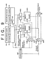
- Fig. 9 is a diagram showing the configuration of a bit deinterleave circuit implemented by the second embodiment of the present invention. Components of the second embodiment substantially identical with those shown in Fig. 23 are denoted by the same reference numerals as the latter.
- the bit deinterleave circuit shown in Fig. 9 deinterleaves a received signal interleaved by the bit interleave circuit shown in Fig. 8.
- the bit deinterleave circuit shown in Fig. 9 is different from the bit deinterleave circuit shown in Fig. 23 in that the former shown in Fig. 9 includes an inverter 142 for inverting the most significant bit (MSB) of the output of a vertical-direction counter 38 employed in a read address counter 140. It should be noted that this embodiment includes the inverter 142 for inverting the most significant bit (MSB) of the output of the vertical-direction counter 38 employed in the read address counter 140 as described above. In place of the inverter 142, this embodiment can include an inverter for inverting the most significant bit (MSB) of the output of a horizontal-direction counter 32 employed in a write address counter 30.
- MSB most significant bit
- this embodiment may include an inverter for inverting the most significant bit (MSB) of the output of a horizontal-direction counter 39 employed in the read address counter 140 or an inverter for inverting the most significant bit (MSB) of the output of a vertical-direction counter 34 employed in the write address counter 30.
- MSB most significant bit
- this alternative configuration the orders of read and write operations are reversed. To be more specific, the order of a read operation begins with an operation in the horizontal direction and ends with an operation in the vertical direction while a write operation begins with an operation in the vertical direction and ends with an operation the horizontal direction.
- Fig. 10 is an explanatory diagram used for describing the operations of the bit interleave circuit and the bit deinterleave circuit shown in Figs. 8 and 9, respectively.
- a horizontal-direction control 6 employed in a write-address counter 30 repeatedly counts the number of clocks synchronized with bits of a transmission signal output by a control circuit 133 from 0 to (n-1).
- a vertical-direction counter 4 also employed in the write-address counter 30 repeatedly counts the number of clock periods from 0 to (m-1). By a clock period, the counting period of the horizontal-direction counter 6 is meant.
- An inverter 132 inverts the MSB of vertical-direction counter 4.
- the output of the horizontal-direction counter 6 and the output of the inverter 132 are supplied to the address terminal of the RAM 16#0 or the RAM 16#1 by way of the selector 14#0 or 14#1, respectively as a lower-order address (also known as a column address) and a most significant bit, respectively.
- the output of the vertical-direction counter 4 except the most significant bit thereof is supplied to the address terminal of the RAM 16#0 or the RAM 16#1 by way of the selector 14#0 or 14#1, respectively as an upper-order address (also known as a row address) excluding the most significant address bit thereof.
- Encoded lists are alternately written into the RAMs 16#0 and 16#1 in bit-interleave-block units each having dimensions of n ⁇ m bits in accordance with a RAM plane switching control signal output by the control circuit 133.
- the most significant bit of the vertical-direction counter 4 is inverted by the inverter 132.
- an interleave block is written into a memory area with a form of a matrix having dimensions of n ⁇ m bits as two sub-blocks.
- the first sub-block that is, the first half of an interleave block
- the second sub-block that is, the second half of the interleave block, is written into the upper half of the memory area.
- a list segment of (0, 1, 2, 3) is written into a vertical-direction address of 2
- a list segment of (4, 5, 6, 7) is written into a vertical-direction address of 3
- a list segment of (8, 9, A, B) is written into a vertical-direction address of 0
- a list segment of (C, D, E, F) is written into a vertical-direction address of 1 as shown in Fig. 10.
- a vertical-direction counter 12 employed in a read-address counter 8 repeatedly counts the number of clocks generated by a control circuit 133 from 0 to (m-1), outputting the clock count to the address terminal of either a RAM 16#0 or a RAM 16#1 by way of a selector 14#0 or 14#1, respectively as an upper-order address (or known as a row address).
- a horizontal-direction counter 10 also employed in the read-address counter 8 repeatedly counts the number of clock periods from 0 to (n-1), outputting the clock-period count to the address terminal of either the RAM 16#0 or the RAM 16#1 by way of the selector 14#0 or 14#1, respectively as a lower-order address (or known as a column address).
- the counting period of the horizontal-direction counter 12 is meant.
- Encoded lists are alternately read out from the RAMs 16#0 and 16#1 in bit-interleave-block units each having dimensions of n ⁇ m bits in accordance with a RAM plane switching control signal.
- the interleaver output is 8, C, 0, 4, 9, D, 1, 5, A, E and so on as shown in Fig. 10.
- the post-interleave distance between two adjacent bits in the same interleave block is m whereas the distance between the last bit in an interleave block and the first bit in the immediately succeeding interleave block is m ⁇ n.
- a horizontal-direction counter 32 and a vertical-direction counter 34 count the number of clocks generated by a control circuit 143 in synchronization with a received signal, outputting the count results to a RAM 42#0 or 42#1 by way of a selector 40#0 or 40#1, respectively.
- the interleave block is written into the RAM 42#0 or 42#1 selected alternately by the RAM plane switching control signal output by the control circuit 143.
- Fig. 11 is a diagram showing outputs of the bit deinterleave circuit shown in Fig. 9.
- the interleaver output is 8, C, 0, 4, 9, 1, 5 and so on as shown in Fig. 11 (a) where the numbers i in the output are order numbers before the bit interleave process carried out on the transmitter side.
- This interleave output is written into a memory area so that a list segment of (8, C, 0, 4) is written into a horizontal-direction address of 0, a list segment of (9, D, 1, 2) is written into a horizontal-direction address of 1, a list segment of (A, E, 2, 6) is written into a horizontal-direction address of 2 and a list segment of (B, F, 3, 7) is written into a horizontal-direction address of 3 as shown in Fig. 10.
- a horizontal-direction counter 39 and a vertical-direction counter 38 count the number of clocks output by a control circuit 143 in synchronization with a received signal whereas an inverter 142 inverts the most significant bit of the vertical-direction counter 38.
- the count results are output to a RAM 42#0 or 42#1 by way of a selector 40#0 or 40#1, respectively.
- selector 40#0 or 40#1 Each time one interleave block is received, interleave blocks are read out sequentially from the RAM 42#0 or 42#1 selected alternately by a RAM plane switching control signal generated by the control circuit 143.
- segment lists are read out from the memory area at a vertical-direction-address order of 2, 3, 0 and 1 to generate a list of (0, 1, 2, 3, 4 and so on) as shown in Figs. 10 and 11A.
- hatched blocks in Fig. 11A the distance between the last bit in an interleave block and the first bit in the immediately succeeding interleave block is 16.
- Fig. 11B is a diagram showing a conventional case in which two consecutive erroneous bits appear as a result of a bit deinterleave process. Deterioration of the BER characteristic in the case shown in Fig. 11A is suppressed more than the case shown in Fig. 11B.
- Fig. 12 is a diagram showing the configuration a bit interleave circuit implemented by a third embodiment of the present invention. Components of the third embodiment substantially identical with those shown in Fig. 22 are denoted by the same reference numerals as the latter.
- the bit interleave circuit implemented by the third embodiment is different from the conventional bit interleave circuit in that:
- Fig. 13 is a diagram showing the configuration of a bit deinterleave circuit implemented by the third embodiment of the present invention.
- Components of the third embodiment substantially identical with those shown in Fig. 23 are denoted by the same reference numerals as the latter.
- the bit deinterleave circuit implemented by the third embodiment is different from the conventional bit deinterleave circuit in that:
- Fig. 14 is an explanatory diagram used for describing the operations of the bit interleave circuit and the bit deinterleave circuit shown in Figs. 12 and 13, respectively.
- the operations of the bit interleave circuit and the bit deinterleave circuit shown in Figs. 12 and 13, respectively are described as follows.
- Fig. 15 shows write time charts of the bit interleave circuit shown in Fig. 12.
- a vertical-direction counter 4 also employed in the write-address counter 150 repeatedly counts the number of clock periods repeatedly from 0 to (m-1), outputting the clock-period count to the address terminal of the RAM 16#0 or the RAM 16#1 by way of the selector 14#0 or 14#1, respectively as an upper-order address.
- the counting period of the horizontal-direction counter 152 is meant.
- a RAM write timing signal generated by the control circuit 151 is made valid by a clock signal synchronized with an encoded list.
- the k-bit parallel encoded list output by an FEC encoding circuit 70 are written into the memory area of the RAM 166#0 or 166#1 selected by the RAM plane switching control signal in interleave-block units by way of gate circuits 168#0, 168#1, 170#0 and 170#1 and data terminals #0 and #1 of the RAM 166#0 or 166#1.
- Fig. 16 shows read time charts of the bit interleave circuit shown in Fig. 12.
- a vertical-direction counter 10 employed in the read address counter 160 repeatedly counts the number of clock periods, which are each equal to 1/k times the clock period generated by the control circuit 151 in synchronization with the encoded list, from 0 to (m-1) and outputs the clock-period count to the address terminal of the RAM 166#0 or 166#1 by way of the selector 14#0 or 14#1, respectively as an upper-order address.
- the horizontal-direction counter 162 also employed in the read address counter 160 repeatedly counts the number of clock periods, which are each equal to k times the counting period of the vertical-direction counter 10, from 0 to (n1-1) and outputs the clock-period count to the address terminal of the RAM 166#0 or 166#1 by way of the selector 14#0 or 14#1, respectively as a lower-order address.
- Each interleave block is read out alternately from the RAM 166#0 or 166#1 through the data terminals #0 and #1 to be output as an interleaved k-bit encoded list.
- the counting to generate vertical-direction addresses 0 to 3 is carried out twice.
- a sequence of 2 bits (0, 1), 2 bits (4, 5), 2 bits (8, 9) and 2 bits (C, D) are read out at the same time from the vertical addresses 0, 1, 2 and 3, respectively.
- a horizontal-direction address of 0 such a sequence is output twice.
- a P/S converter 176 sequentially selects data received from one of outputs #i of the k data terminals of the RAM 166#0 or 166#1 by way of selectors 172 and 174 in accordance with a P/S control signal generated by the control circuit 151 in synchronization with the counting periods of the read address counter 160.
- k 2
- the output #0 is selected before selection of the output #1.
- the bit interleave circuit outputs a list of (0, 4, 8, C, 1, 5, 9, D, 6, A, E, 3, 7, B) much like the conventional circuit.
- the clock period of the horizontal-direction counter 152 employed in the bit interleave circuit is only a half of that of the conventional circuit, resulting in improvements such as reduction of the power consumption.
- the power consumption can be reduced by having the circuit operate slower.
- a signal output by the modulator is subjected to a frequency transformation process in an RF unit before being transmitted from an antenna.
- Fig. 17 shows write time charts of the bit deinterleave circuit shown in Fig. 13.
- a vertical-direction counter 34 employed in a write address counter 180 repeatedly counts the number of clocks output by a control circuit 183 in synchronization with input events of a received signal from 0 to (m-1) and outputs the clock count to the address terminal of a RAM 192#0 or 192#1 by way of a selector 40#0 or 40#1, respectively as an upper-order address.
- a RAM write timing signal generated by the control circuit 183 is made valid by a clock signal synchronized with input of a received signal. Each input interleave block is supplied to the RAM 192#0 or 192#1 selected alternately by way of a gate circuit 44#0 or 44#1, respectively.
- a D-FF write timing signal generated by the control circuit 183 is made valid by a clock signal synchronized with input of a received signal, being supplied to a clock terminal of a D-FF 196#0 or 196#1 by way of a gate circuit 194#0 or 194#1, respectively.
- the received signal is supplied to a selector 198#0 and the data terminal #1 of the RAM 192#0 by way of a gate circuit 46#0 or a selector 198#1 and the data terminal #1 of the RAM 192#1 by way of a gate circuit 46#1.
- the selectors 198#0 and 198#1 select received signals during (k-1)counting periods of the vertical-direction counter 34 and select outputs of the D-FFs 196#0 and 196#1, respectively during the last counting period of the vertical-direction counter 34, outputting the selected outputs to the (k-2) data terminals of either the RAM 192#0 or 192#1, respectively.
- pieces of data from the outputs terminals of (k-2) D-FFs are supplied to the data terminals of the RAM 192#0 or the RAM 192#1.
- the (k-2) D-FFs are selected among the ( (k-1) ⁇ m + 1 ) D-FFs connected to each other in cascade, starting with the D-FF at the last stage at intervals of m D-FFs.
- received signals 0, 4, 8 and C are once latched in the D-FF 196#0 or 196#1 before being supplied to the data terminal #0 of the RAM 192#0 or 192#1 from the D-FF at the last stage by way of the selector 198#0 or 198#1, respectively after four clocks have lapsed since the latching of the received signals to be written into the RAM 192#0 or 192#1 as shown in Fig. 17.
- received signals (1, 5, 9 and D) are sequentially supplied to the data terminal of the RAM 192#0 or 192#1 to be written therein.
- n 4
- received signals (0, 1), (4,5), (8, 9), (C, D) are written into vertical-direction addresses of 0, 1, 2 and 3, respectively
- received signals (2, 3), (6, 7), (A, B) and (E, F) are written into vertical-direction addresses of 0, 1, 2 and 3, respectively.
- Fig. 18 shows write time charts of the bit deinterleave circuit shown in Fig. 13.
- a horizontal-direction counter 188 employed in a read address counter 186 repeatedly counts the number of clock periods, which are each equal to k times the input period of a received signal, from 0 to (n1-1) and outputs the clock-period count to the address terminal of the RAM 192#0 or 192#1 by way of a selector 40#0 or 40#1, respectively as a lower-order address.
- a vertical-direction counter 38 also employed in the read address counter 186 repeatedly counts the number of clock periods from 0 to (m-1) and outputs the clock-period count to the address terminal of the RAM 192#0 or 192#1 by way of the selector 40#0 or 40#1, respectively as an upper-order address.
- the counting period of the horizontal-direction counter 188 is meant.
- k bits are output in parallel from k data terminals either of the RAM 192#0 or 192#1 as a result of a bit deinterleave process to an FEC decoder 144 by way of selectors 200 and 202.
- the result of the bit deinterleave process is a series of two parallel bits (0, 1), (2, 3), (4, 5), (6, 7) and so on.
- the FEC decoder 144 receives k parallel bits as an output of the bit deinterleave process, decoding the bits by adopting typically the viterbi decoding technique.
- the horizontal-direction counter 188 of the read address counter 186 employed in the bit deinterleave circuit can be operated and the read operations of the RAMs 192#0 and 192#1 can be carried out at a clock period equal to k times the clock period of the received signal, so that the power consumption can be reduced.
- Fig. 19 is a diagram showing the configuration of the bit interleave circuit implemented by a fourth embodiment.
- Components of the fourth embodiment substantially identical with those of the bit interleave circuit shown in Fig. 12 are denoted by the same reference numerals as the latter.
- the bit interleave circuit shown in Fig. 19 is different from the bit interleave circuit shown in Fig. 12 in that, in the case of the former:
- Fig. 20 is an explanatory diagram used for explaining the operation of the bit interleave circuit shown in Fig. 19.
- the operation of the bit interleave circuit shown in Fig. 19 is explained as follows.
- a clock period k times the counting period of the horizontal-direction counter 152 is meant.
- a RAM write timing signal is supplied to either the gate circuit 222#0 for the RAM 218#0 serving as a 0-plane, the gate circuit 224#0 for the RAM 220#0 serving as a 0-plane, the gate circuit 222#1 for the RAM 218#1 serving as a 1-plane or the gate circuit 224#1 for the RAM 220#1 serving as a 1-plane.
- One of the gate circuits 220#0 and 224#0 is selected alternately by a gate control signal.
- one of the gate circuits 220#1 and 224#1 is selected alternately by the gate control signal.
- the write operation is alternately switched between the RAM 218#0 serving as a 0-plane and the RAM 220#0 serving as a 0-plane for two encoded list segments on two consecutive horizontal-direction rows in the interleave-block matrix by the gate control signal.
- the write operation is alternately switched between the RAM 218#1 serving as a 1-plane and the RAM 220#1 serving as a 1-plane for two encoded list segments on two consecutive horizontal-direction rows in the interleave-block matrix by the gate control signal.
- a parallel encoded list is thus written into an area specified by an address in the RAM 218#0, 220#0, 218#1 or 220#1.
- Fig. 21 is an explanatory diagram used for explaining the read operation of the bit interleave circuit shown in Fig. 19.
- the control circuit 211 outputs selector control signals to selectors 226#0 and 228#0 or 226#1 and 228#1 so as to sequentially select signals output by data terminals associated with either pair of selectors from a column on the left end to a column on the right end. As shown in Fig.
- a vertical-direction counter 216 employed in a read address counter 214 repeatedly counts the number of clocks output by the control circuit 211 from 0 to (m1-1) and outputs the clock count to the address terminals of RAMs 218#0 and 220#0 or 218#1 and 220#1 by way of a selector 14#0 or 14#1, respectively as an upper-order address.
- a horizontal-direction counter 162 also employed in the read address counter 214 repeatedly counts the number of clock periods from 0 to (n1-1) and outputs the clock-period count to the address terminals of the RAMs 218#0 and 220#0 or 218#1 and 220#1 by way of the selector 14#0 or 14#1, respectively as a lower-order address.
- k times the counting period of the vertical-direction counter 216 is meant. Encoded lists are read out from k data terminals of the RAMs 218#0 and 220#0 or 218#1 and 220#1.
- the control circuit 211 outputs selector control signals to selectors 226#0 and 228#0 or 226#1 and 228#1 so as to sequentially select signals output by data terminals associated with either pair of selectors from a column on the left end to a column on the right end in synchronization with a count period of the vertical-direction counter 216.
- the selected signals are output to a P/S converter 176 by way of selectors 172 and 174.
- the vertical addresses are 0, 1, 0 and 1.
- outputs #0 and #2 are selected to output list segments (0, 4) and (8, C) sequentially as shown in Fig. 21.
- outputs #1 and #3 are selected to output list segments (1, 5) and (9, D) sequentially.
- the P/S converter 176 converts the parallel interleaver output into serial data.
- the clock period of the vertical-direction counter 216 employed in the read address counter 214 is longer than that of the bit interleave circuit implemented by the third embodiment, the power consumption can be further reduced. It should be noted that a combination of the bit interleave circuits provided by the first, second and third embodiments can of course be implemented.
- the present invention if the reception level of a bit of a received signal completing an interleave process is lower than a threshold value, a command signal requesting that computation be inhibited is issued for the bit. As a result, the BER characteristic can be prevented from deteriorating.
- the distance between the last bit of an interleave block and the first bit of the immediately succeeding interleave block can be set at least at 2, a burst error can be randomized. As a result, an error correction capability can be enhanced. Furthermore, since the operating-clock frequency can be reduced, the power consumption decreases.
Abstract
Description
- In general, The present invention relates to a bit interleave circuit and a bit deinterleave circuit which are used in a mobile communication system or a mobile broadcasting system.
- In a system where information is communicated or broadcasted by using a radio wave to a movable body such as an automobile, there is a problem of deterioration in quality of communication due to attenuation of received power which is caused by shadowing or fading. Shadowing is a phenomenon in which an electric wave is blocked by a building or the like. On the other hand, fading is a phenomenon in which interference between multipath delayed waves occurs. In particular, when an FEC (Forward Error Correction) apparatus is used for improving the quality of communication, the ability to correct an error deteriorates in case a burst error is generated by shadowing or fading, raising a problem of a substantially deteriorating quality of communication.
- In order to prevent the quality of communication from considerably deteriorating due to shadowing or fading, a bit interleave circuit and a bit deinterleave circuit are employed on the transmitter and receiver sides, respectively in many cases. To put in detail, a random-access memory with a 2-plane configuration is employed so as to allow a series of output codes generated by an error correction encoder to be transmitted by changing the order of the codes in accordance with a proper rule. On the receiver side, on the other hand, the received codes are rearranged in the reverse order to reproduce the original series of codes which is then supplied to an error correction decoder. In this way, burst errors generated along the radio transmission path can be randomized so that the deterioration of the ability to correct an error is reduced.
- Fig. 22 is a diagram showing the configuration of the conventional bit interleave circuit and Fig. 23 is a diagram showing the configuration of the conventional bit deinterleave circuit. Fig. 24 is an explanatory diagram used for describing the operations of the bit interleave and bit deinterleave circuits shown in Figs. 22 and 23 respectively for an interleave block of 4 × 4 bits.
- As shown in Fig. 24, information coded by an
FEC encoder 50 by adopting a convolution encoding technique or the like is converted into serial data by a P/S converter 52 before being fed to thebit interleave circuit 54 shown in Fig. 22. In thebit interleave circuit 54, a horizontal-direction counter 6 employed in a write-address counter 2 counts the number of clocks synchronized with an input signal repeatedly from 0 to 3, outputting the clock count to an address terminal of either aRAM 16#0 or aRAM 16#1 by way of aselector 14#0 or 14#1, respectively as a lower-order address. - On the other hand, a vertical-
direction counter 4 also employed in the write-address counter 2 counts the number of clock periods repeatedly from 0 to 3, outputting the clock-period count to the address terminal of either theRAM 16#0 or theRAM 16#1 by way of theselector 14#0 or 14#1, respectively as an upper-order address. By a clock period, the counting period of the horizontal-direction counter 6 is meant. A RAM plane switching control signal controls theRAMs 16#0 and 16#1 so that their write-in and read-out operations are mutually exclusive. To be more specific, when a read operation is carried out on one of theRAMs 16#0 or 16#1, a write operation is carried out on the other. - A
gate circuit 18#0 supplies a RAM write timing signal to a write enable terminal WE of theRAM 16#0 in accordance with the RAM plane switching control signal. By the same token, agate circuit 18#1 supplies a RAM write timing signal to a write enable terminal WE of theRAM 16#1 in accordance with the RAM plane switching control signal. Agate circuit 20#0 receives a serial transmission signal (0 to F), outputting the signal to aterminal data # 0 of theRAM 16#0 in accordance with the RAM plane switching control signal. By the same token, agate circuit 20#1 receives a serial transmission signal (0 to F), outputting the signal to aterminal data # 0 of theRAM 16#1 in accordance with the RAM plane switching control signal. It should be noted that thereference numerals 0 to F are hexadecimal numbers representing the contents of the encoded list. - When the RAM write timing signal supplied to the write enable terminal WE of the
RAM 16#0 or 16#1 is active, the encoded list supplied to theterminal data # 0 is written into a location in theRAM 16#0 or 16#1 indicated by the address signal supplied to the address terminal. As a result, the contents of the i-th encoded list are written into a location at the address i as shown in Fig. 24. A vertical-direction counter 12 employed in a read-address counter 8 repeatedly counts the number of clocks synchronized with an input signal from 0 to 3, outputting the clock count to the selector either 14#0 or 14#1, respectively as an upper-order address. - On the other hand, a horizontal-
direction counter 10 also employed in the read-address counter 8 counts the number of clock periods repeatedly from 0 to 3, outputting the clock-period count to the address terminal of either theRAM 16#0 or theRAM 16#1 by way of theselector 14#0 or 14#1, respectively as a lower-order address. By a clock period, the counting period of the vertical-direction counter 12 is meant. Either of theRAMs 16#0 and the 16#1 outputs an encoded list from a location indicated by an address supplied to the address terminal thereof to a transmission system by way of aselector 22. In this way, the signal to be transmitted is interleaved in the order of 0, 4, 8, C, 1, 5, 9 and so on. - In the bit
deinterleave circuit 56 shown in Fig. 23, a vertical-direction counter 34 employed in a write-address counter 30 counts the number of clocks synchronized with an input signal, repeatedly from 0 to 3, outputting the clock count to the address terminal of either aRAM 42#0 or aRAM 42#1 by way of aselector 40#0 or 40#1, respectively as an upper-order address. On the other hand, a horizontal-direction counter 32 also employed in the write-address counter 30 counts the number of clock periods repeatedly from 0 to 3, outputting the clock-period count to the address terminal of either theRAM 42#0 or theRAM 42#1 by way of theselector 40#0 or 40#1, respectively as a lower-order address. By a clock period, the counting period of the vertical-direction counter 34 is meant. Data supplied to theterminal data # 0 is written into a location in theRAM 42#0 or 42#1 indicated by the address signal supplied to the address terminal. As a result, a signal i received in the order of 0, 4, 8, C, 1 and so on is written at an address i where i is the order number of the encoded list prior to the interleave process. - A horizontal-
direction counter 39 employed in a read-address counter 36 repeatedly counts the number of clocks synchronized with an input signal from 0 to 3, outputting the clock count to the address terminal of either theRAM 42#0 or theRAM 42#1 by way of theselector 40#0 or 40#1, respectively as a lower-order address. On the other hand, a vertical-direction counter 38 also employed in the read-address counter 36 counts the number of clock periods repeatedly from 0 to 3, outputting the clock-period count to the address terminal of either theRAM 42#0 or theRAM 42#1 by way of theselector 40#0 or 40#1, respectively as an upper-order address. By a clock period, the counting period of the horizontal-direction counter 39 is meant. - Either one of the
RAMs 42#0 or the 42#1 outputs an encoded list from a location indicated by an address signal supplied to the address terminal by way of aselector 48. In this way, the received signal is correctly deinterleaved to thepreinterleave order - In addition, when erroneous coded bits are supplied to the FEC decoder at the same time, the ability to correct an error deteriorates as is generally known. The probability of erroneous bits' being received at the same time increases as a burst error is generated on the radio transmission path. In order to solve this problem, the parallel output of the FEC encoder is converted into serial data prior to an bit interleave process in the conventional mobile communication/broadcasting system. On the receiver side, on the other hand, received serial data is converted into parallel data after a bit deinterleave process. In this way, it is possible to prevent input bits from becoming erroneous at the same time.
- For the reason described above, it is necessary to operate the bit interleave circuit and bit deinterleave circuits employed in the conventional mobile communication/broadcasting system at a clock rate equal to the bit rate of codes. Fig. 24 is a diagram showing examples of operations carried out at a coding rate of 1/2. In this case, it is necessary to write and read data into and from a RAM at a clock rate twice as much as the bit rate of the information. In consequence, among other problems, there is raised an issue that not only is it difficult to implement a bit interleave circuit capable of operating at a high speed, but the amount of power consumption also increases as well.
- It is thus an object of the present invention addressing the problems described above to provide a bit interleave circuit and a bit deinterleave circuit for implementing prevention of errors from further deteriorating and for implementing reduction of the power consumption by carrying out operations at a low speed.
- In accordance with one aspect of the present invention, there is provided a bit deinterleave circuit bit deinterleaving a signal, the bit deinterleave circuit comprising: measurement means for measuring the reception level of each bit in a received signal completing a bit interleave process; command-signal generating means for outputting a command signal to indicate whether computation in error correction is to be inhibited or permitted for said bit on the basis of said reception level of each bit measured by said measurement means and a threshold value; first deinterleave means for deinterleaving said received signal completing a bit interleave process; and second deinterleave means for rearranging said command signals so as to output command signals according to a signal output by said first deinterleave means.
- In accordance with another aspect of the present invention, there is provided a bit interleave circuit bit interleaving a signal, the bit interleave circuit comprising:random-access memory allowing operations based on an address signal to write and read data; first counter for carrying out a counting operation synchronized with an input encoded list and outputting a lower-order address of said address signal; second counter for carrying out a counting operation synchronized with counting periods of said first counter and outputting an upper-order address of said address signal; third counter for carrying out a counting operation synchronized with said input encoded list and outputting an upper-order address of said address signal; fourth counter for carrying out a counting operation synchronized with counting periods of said third counter and outputting a lower-order address of said address signal; and inverter circuit for inverting the most significant bit of either said second counter or said third counter.
- The above and other objects, features and advantages of the present invention as well as the manner of realizing them will become more apparent, and the invention itself will be best understood from a study of the following description and appended claims with reference to attached drawings showing some preferred embodiments of the invention.
-
- Fig. 1 is a diagram showing the principle of the present invention;
- Fig. 2 is a diagram showing a configuration of a radio set including a bit interleave circuit and a bit deinterleave circuit which are implemented by a first embodiment of the present invention;
- Fig. 3 is a diagram showing the configuration of the bit deinterleave circuit implemented by the first embodiment of the present invention;
- Fig. 4 is a block diagram showing the computation-inhibit-signal generating circuit employed in the bit deinterleave circuit shown in Fig. 3;
- Fig. 5 is an explanatory diagram used for describing the operation of the bit deinterleave circuit shown in Fig. 3;
- Fig. 6 is a diagram showing a computation-inhibit command signal;
- Fig. 7 is an explanatory diagram showing effects of the bit deinterleave circuit shown in Fig. 3;
- Fig. 8 is a diagram showing the configuration of a bit interleave circuit implemented by a second embodiment of the present invention;
- Fig. 9 is a diagram showing the configuration of a bit deinterleave circuit implemented by the second embodiment of the present invention;
- Fig. 10 is an explanatory diagram used for describing the operations of the bit interleave circuit and the bit deinterleave circuit shown in Figs. 8 and 9, respectively;
- Fig. 11A is a diagram showing output of a bit deinterleave circuit shown in Fig.9;
- Fig. 11B is a diagram showing a conventional case in which two consecutive erroneous bits appear result of bit deinterleave process;
- Fig. 12 is a diagram showing the configuration of a bit interleave circuit implemented by a third embodiment of the present invention;
- Fig. 13 is a diagram showing the configuration of a bit deinterleave circuit implemented by the third embodiment of the present invention;
- Fig. 14 is an explanatory diagram used for describing the operations of the bit interleave circuit and the bit deinterleave circuit shown in Figs. 12 and 13, respectively;
- Fig. 15 shows write time charts of the bit interleave circuit shown in Fig. 12;
- Fig. 16 shows read time charts of the bit interleave circuit shown in Fig. 12;
- Fig. 17 shows write time charts of the bit deinterleave circuit shown in Fig. 13;
- Fig. 18 shows read time charts of the bit deinterleave circuit shown in Fig. 13;
- Fig. 19 is a diagram showing the configuration of a bit interleave circuit implemented by a fourth embodiment of the present invention;
- Fig. 20 is an explanatory diagram used for explaining the write operation of the bit interleave circuit shown in Fig. 19;
- Fig. 21 is an explanatory diagram used for explaining the read operation of the bit interleave circuit shown in Fig. 19;
- Fig. 22 is a diagram showing the configuration of the conventional bit interleave circuit;
- Fig. 23 is a diagram showing the configuration of the conventional bit deinterleave circuit; and
- Fig. 24 is an explanatory diagram used for describing the operations of the bit interleave and bit deinterleave circuits shown in Figs. 22 and 23, respectively.
-
- Before preferred embodiments of the present invention are explained, first of all, a principle underlying the invention is described by referring to Fig. 1. As shown in the figure, a bit deinterleave circuit comprises: a measurement means 62 for measuring the reception level of each bit in a received signal completing a bit interleave process; a command-signal generating means 64 for outputting a command signal to indicate whether computation in error correction is to be inhibited or permitted for each bit on the basis of the reception level of the bit measured by the measurement means 62 and a threshold value; a first deinterleave means 66 for deinterleaving the received signal completing a bit interleave process; and a second deinterleave means 68 for rearranging command signals so as to output the command signals according to a signal output by the first deinterleave means 66.
- In such a configuration, the reception level measured by the measurement means 62 is information on the amplitude of each bit in a received signal completing a bit interleave process. This is because fading or shadowing attenuates the reception level and the reception-level attenuation makes the reception characteristic deteriorate. The command-signal generating means 64 compares the reception level of each bit measured by the measurement means 62 with a threshold value. For example, if the reception level of a bit is found lower than the threshold value, a command signal is issued to request that computation be inhibited as shown by an X mark in the figure. If the reception level of a bit is found higher than the threshold value, on the other hand, a command signal is issued to indicate that computation is allowed as shown by an ○ mark in the figure. Assume that the reception level of a bit is lower than the threshold value during the period t0 to t1. In this case, a command signal is issued to request that computation be inhibited during this period.
- The first deinterleave means 66 deinterleaves the received signal completing a bit interleave process by rearranging bits in the signal. The second deinterleave means 68 rearranges command signals to output the command signals according to bits of a signal output by the first deinterleave means 66. An
FEC decoder 69 receives bits of the received signal completing the bit deinterleave process and the command signals according to the bits. If a command signal for a bit indicates that computation is inhibited, a decoding process is carried out by excluding the bit from decoding computation. In this way, a BER characteristic can be prevented from deteriorating. - Fig. 2 is a diagram showing a radio set including a bit interleave circuit and a bit deinterleave circuit which are implemented by a first embodiment of the present invention. The radio set is a mobile station or a base station used in a mobile communication system or the like. As shown in the figure, the radio set comprises an
FEC encoder 70, an P/S converter 71, a bitinterleave circuit 72, amodulator 74, anRF unit 76,antennas RF unit 82, ademodulator 84, an A/D converter 85, a bitdeinterleave circuit 86, an S/P converter 87 and anFEC decoder 88. - The
FEC encoder 70 carries out an encoding process at a fixed encoding rate such as the convolution encoding process on incoming information to generate an encoded list of k bits. The P/S converter 71 converts the k-bit parallel data into serial data. The bit interleavecircuit 72 carries out a bit interleave process on encoded serial data in a configuration like the one shown in Fig. 22. Themodulator 74 modulates a signal completing the bit interleave process by adopting a predetermined modulation method such as the BPSK or QPSK. TheRF unit 76 transforms frequencies of the modulated signal into a fixed frequency band and amplifies the signal. Theantenna 78 transmits a transmission signal. - On the other hand, the
antenna 80 receives a radio signal. TheRF unit 82 extracts a signal in a fixed frequency band and carries out processing such as amplification on the extracted signal. The demodulator 84 measures the level of the received signal to output an RSSI (Received Signal Strength Indicator). At the same time, thedemodulator 84 controls the amplitude of the received signal by using an AGC circuit and demodulates the received signal which was modulated by the BPSK or QPSK method, outputting a demodulated signal including amplitude information. Thedemodulator 84 generates a demodulated signal including amplitude information in order to increase the error correction capability of theFEC decoder 88. The A/D converter 85 converts the demodulated signal into a digital signal comprising a fixed number of quantization bits. Typically, the number of quantization bits is 3 with the code bit of the most significant code bit being an encoded bit. - Fig. 3 is a diagram showing the configuration of the bit
deinterleave circuit 86 shown in Fig. 2. Components of the bit deinterleave circuit substantially identical with those shown Fig. 23 are denoted by the same reference numerals as the latter. As shown in Fig. 3, the bitdeinterleave circuit 86 comprises acontrol circuit 90, adelay circuit 92, a computation-inhibit-signal generating circuit 94, awrite address counter 30, aread address counter 36,selectors 40#0 and 40#1,RAMs 42#0 and 42#1,gate circuits 44#0, 44#1, 46#0 and 46#1, aselector 48, awrite address counter 96, aread address counter 102,selectors 108#0 and 108#1,RAMs 110#0 and 110#1,gate circuits 112#0, 112#1, 114#0 and 114#1 and aselector 116. It should be noted that theRAMs 42#0 and 42#1 each have a width of 1 bit, and as many such RAMs as bits output by the A/D converter 85 are provided. - The
control circuit 90 generates a clock signal synchronized with a received signal. In addition, thecontrol circuit 90 also generates a RAM plane switching control signal and a RAM write timing signal for each interleave block of n × m bits in synchronization with the clock signal where the symbol n is the number of bits in the horizontal direction in the block whereas the symbol m is the number of bits in the vertical direction in the block. Thedelay circuit 92 is typically implemented by a shift register which operates on the basis of a clock signal synchronized with a received signal. Thedelay circuit 92 delays the received signal completing a bit interleave process by a predetermined delay time equal in length to a period between reception of bits of the received signal and generation of command signals by the computation-inhibit-signal generating circuit 94 to indicate that computation be inhibited or allowed for the bits. - Fig. 4 is a block diagram showing the computation-inhibit-
signal generating circuit 94 employed in the bitdeinterleave circuit 86 shown in Fig. 3. As shown in Fig. 4, the computation-inhibit-signal generating circuit 94 comprises amobile averaging circuit 122, aweight providing circuit 124 and acomparator 126. Themobile averaging circuit 122 detects the envelop of an analog signal output by thedemodulator 84 and measures the level of the received signal. To be more specific, themobile averaging circuit 122 measures the reception level of each bit in the received signal and computes an average of reception levels of bits in the received signal within a predetermined range preceding and succeeding the bit. Such an average is referred to hereafter as a mobile average. A mobile average is found in order to suppress an effect of noise generated by the radio set. This is because fading or shadowing attenuates the reception level and the reception-level attenuation gives rise to a continuous burst error. - The
weight providing circuit 124 provides weights to reception levels of bits, which were subjected to the mobile-averaging process. The weights are found from the RSSI signal or an AGC control voltage output by thedemodulator 84. For example, the reception levels of the bits are multiplied by the RSSI signal or the AGC control voltage. Weights are provided to the reception levels because of the following reason. Since the AGC circuit employed in thedemodulator 84 adjusts the level of the received signal, from only the level of a signal output by thedemodulator 84, it is impossible to determine the level which the received signal had at the time the received signal arrived theantenna 80. It is thus necessary to return the level of the received signal to that of the received signal which had at the time the received signal arrived at theantenna 80. - The
comparator 126 compares the level of the received signal output by theweight providing circuit 124 with a threshold value (or a reference voltage). If the level of the received signal output by theweight providing circuit 124 exceeds the threshold value, thecomparator 126 outputs a command signal set typically at a low level indicating that computation is allowed. If the level of the received signal output by theweight providing circuit 124 is equal to or lower than the threshold value, on the other hand, thecomparator 126 outputs a command signal raised typically to a high level indicating that computation is inhibited. If thecomparator 126 outputs a command signal indicating that computation is inhibited for a received signal, theFEC decoder 88 inhibits error-correction computation for the received signal with which the command signal is associated. - This is because, rather than applying error correction to the received signal as it is, a BER characteristic can be improved as is disclosed for example in a thesis authored by Yasuda et al. with a title of "High-Encoding-Rate Convolution with Easy Viterbi Decoding and its Characteristics," Communication Theory B, Vol. J64B, No. 7, pp. 573 to 580 (1981). As described above, the bit
deinterleave circuit 86 shown in Fig. 3 comprises thewrite address counter 96, the readaddress counter 102, theselectors 108#0 and 108#1, theRAMs 110#0 and 110#1, thegate circuits 112#0, 112#1, 114#0 and 114#1 and theselector 116, those serve as a deinterleaver for deinterleaving command signals. Thewrite address counter 96 includes a horizontal-direction address counter 98 and a vertical-direction address counter 100. By the same token, the readaddress counter 102 includes a horizontal-direction counter 106 and a vertical-direction counter 104. - Except for the fact that a command signal is supplied to the
gate circuits 114#0 and 114#1, the operation of this deinterleaver is substantially the same as that of thewrite address counter 30, the readaddress counter 36, theselectors 40#0 and 40#1, theRAMs 42#0 and 42#1, thegate circuits 44#0, 44#1, 46#0 and 46#1 and theselector 48. It should be noted that thewrite address counter 96, the readaddress counter 102, theselectors 108#0 and 108#1 as well as thegate circuits 112#0 and 112#1 can be shared with the deinterleaver of the received signal. - The operation of the radio set shown in Fig. 2 is explained as follows. Assume that the
antenna 80 shown in Fig. 2 receives a modulated signal which was processed by using the same encoding system as theFEC encoder 70, the same bit interleave system as the bitinterleave circuit 72 and the same modulation system as themodulator 74. Examples of the encoding system, the bit interleave system and the modulation system are the convolution encoding technique, the 4 × 4 interleave blocking technique and the BPSK modulation method, respectively. TheRF unit 82 extracts a signal of a fixed frequency band from the signal received by theantenna 80. Thedemodulator 84 finds an RSSI signal from the received signal and then, after executing AGC control, demodulates the received signal, which was modulated by using typically the BPSK method, into a signal including amplitude information. The modulated signal is then supplied to the A/D converter 85. On the other hand, the RSSI signal and the AGC control voltage are supplied to the bitdeinterleave circuit 86. - The A/
D converter 85 converts the modulated signal received thereby into a digital signal with a fixed number of quantization bits. The coded bits of the quantization bits are encoded bits completing a bit interleave process and the remaining bits represent amplitude information. Fig. 5 is an explanatory diagram used for describing the operation of the bit deinterleave circuit shown in Fig. 3. Thecontrol circuit 90 generates a clock signal synchronized with a received signal. In addition, thecontrol circuit 90 also generates a RAM plane switching control signal and a RAM write timing signal each time a bit interleave block of typically 4 × 4 bits is received. Thedelay circuit 92 delays the received signal by a fixed period of time in order to synchronize the bits of the received signal with command signals each indicating whether computation is inhibited or permitted. - The
mobile averaging circuit 122 shown in Fig. 4 measures the level of the amplitude of the received signal by detecting typically the envelop of the received signal. Themobile averaging circuit 122 then finds an average of the levels of the received signal in a predetermined range including bits of the received signal, supplying the average to theweight providing circuit 124. Theweight providing circuit 124 provides weights to a signal output by themobile averaging circuit 122. The weights are based on the RSSI signal and the AGC control voltage. For example, the signal output by themobile averaging circuit 122 is multiplied by the RSSI signal and the AGC control voltage. The weighted signal is then supplied to thecomparator 126. - The
comparator 126 compares the level of the received signal output by theweight providing circuit 124 with a threshold value (or a reference voltage). If the level of the received signal output by theweight providing circuit 124 exceeds the threshold value, thecomparator 126 outputs a computation-permit command signal set typically at a low level indicating that computation is allowed. If the level of the received signal output by theweight providing circuit 124 is equal to or lower than the threshold value, on the other hand, thecomparator 126 outputs a computation-inhibit command signal raised typically to a high level indicating that computation is inhibited. Thecomparator 126 outputs the command signal to thegate circuits 114#0 and 114#1 shown in Fig. 3. Fig. 6 is a diagram showing the computation-inhibit command signal output by thecomparator 126. As shown in Fig. 6, during the period t1 to t2 in which the level of a received signal is lower than the threshold value due to fading, shadowing or the like, the computation-inhibit command signal is active, being typically raised to a high level. During other periods in which the level of a received signal is higher than the threshold value, the computation-permit command signal is active, being typically set a low level. - The
write address counter 30, theselectors 40#0 and 40#1 as well as thegate circuits 44#0, 44#1, 46#0 and 46#1 cause one interleave block (0, 4, 8, C and so on) to be written into either theRAM 42#0 or 42#1 at addresses (0, 4, 8, C and so on), respectively as shown in Fig. 5. In the mean time, thewrite address counter 96, theselectors 108#0 and 108#1 as well as thegate circuits 112#0, 112#1, 114#0 and 114#1 cause command signals (○, X, X, X, ○ and so on) for the 1-block bits (0, 4, 8, C and so on) to be written into either theRAM 110#0 or 110#1 at the same addresses as the block bits have been written as shown in Fig. 5. - On the other hand, the read
address counter 36 as well as theselectors 40#0 and 40#1 cause 1-block bits (0, 1, 2, 3, 4 and so on) to be read out from either theRAM 42#0 or theRAM 42#1 and deinterleaved before being supplied to the S/P converter 87 by way of theselector 48 as shown in Fig. 5. In the mean time, the readaddress counter 102 as well as theselectors 108#0 and 108#1 cause command signals (○, ○, ○, ○, X and so on) for the 1-block bits (0, 1, 2, 3, 4 and so on) to be read out from either theRAM 110#0 or theRAM 110#1 before being supplied to the S/P converter 87 by way of theselector 116 as shown in Fig. 5. - The S/
P converter 87 converts each of deinterleaver outputs (0, 1, 2, 3, 4 and so on) of the received signal and deinterleaver outputs (○, ○, ○, ○, X and so on) of the command signals into k-bit parallel data which is then output to theFEC decoder 88. TheFEC decoder 88 receives the parallel data from the S/P converter 87, decoding the data by adoption of typically the viterbi decoding technique. In the decoding process, an interleaver output is set at a value having no effect on a judgment if the computation-inhibit command signal for the interleaver output is active. In this way, error computation for an erroneous code caused by fading, shadowing or the like is inhibited. As a result, deterioration of the BER characteristic after the error correction can be suppressed. - Fig. 7 is an explanatory diagram showing effects of the bit deinterleave circuit shown in Fig. 3. The horizontal axis of Fig. 7 represents a ratio Es/No [dB] where the symbol Es is an encoding energy per bit and the symbol No is an energy per 1Hz of noise. On the other hand, the vertical axis represents the BER. The figure shows curves for cases with and without the computation-inhibit command signal. In both the cases, the encoding rate R = 1/2, the number of stages in the shift register k = 7, the number of quantization bits Q = 3, the truncation length of viterbi decoding = 64, the interleave block length = 32 × 256 bits, the shadowing length (a segment of computation inhibition due to shadowing) = 2,736 bits and the depth of the reception level caused by shadowing = -20 dB. As shown in the figure, in the case with a computation-inhibit command signal, the BER is small in comparison with the case without a computation-inhibit command signal. It is thus obvious from the figure that deterioration of the BER characteristic caused by fading, shadowing or the like can be suppressed.
- Fig. 8 is a diagram showing the configuration of a bit interleave circuit implemented by a second embodiment of the present invention. Components of the second embodiment identical with those shown in Fig. 22 are denoted by the same reference numerals as the latter. The bit interleave circuit implemented by the second embodiment is different from the conventional bit interleave circuit in that, in the case of the former, a post-interleave distance between two adjacent bits in the same interleave block is kept at least at a predetermined value. In addition, in the case of the second embodiment, the distance between the last bit in an interleave block and the first bit in the immediately succeeding interleave block is set at least 2.
- The bit interleave circuit shown in Fig. 8 is different from the bit interleave circuit shown in Fig. 22 in that the former of Fig. 8 includes an
inverter 132 for inverting the most significant bit (MSB) of the output of the vertical-direction counter 4 employed in thewrite address counter 130. Theinverter 132 is provided for the following reason. Assume that theRAMs 16#0 and 16#1 are each a memory area with a matrix form of n × m bits where the symbol n is the number of bits in the horizontal direction and the symbol m is the number of bits in he vertical direction. The memory area is divided into two blocks, namely, an upper-side block and a lower-side block. Bits in the first half of an interleave block are written sequentially into the lower-side block of the memory area and bits in the remaining second half of the interleave block are written sequentially into the upper-side block of the memory area. - As a result, the post-interleave distance between two adjacent bits in the same interleave block is m whereas the distance between the last bit in an interleave block and the first bit in the immediately succeeding interleave block is n × m. In addition, the post-interleave distance between two adjacent bits in the same interleave block and in the adjacent blocks is set at least at a predetermined value. In the case of a 4 × 4 interleave block, for example, the post-interleave distance between two consecutive bits has a maximum value of 16 bits, a minimum value of 4 bits and an average value of 6.9 bits. These values are larger than the conventional post-interleave distance between two consecutive bits which has a maximum value of 11 bits, a minimum value of 1 bit and an average value of 5.1 bits, respectively.
- As described above, the
RAMs 16#0 and 16#1 employed in this embodiment are each a memory area with a matrix form divided into two blocks (an upper and a lower portions). It should be noted the memory area can also be divided into three or more blocks into which bits of an interleave block are written. In this case, a plurality of most significant bits in the vertical-direction counter 4 are inverted. In addition, data can be stored in the upper-side and lower-side blocks in this embodiment in the same way as the conventional system. In this case, an inverter is typically provided to invert the most significant bit of a vertical-direction counter 12 employed in aread address counter 8. In such a configuration, after bits of the lower-side block are read out in the vertical direction, bits of the upper-side block are read out in the vertical direction. - Furthermore, in a bit interleave circuit, instead of a write operation in the horizontal direction shown in Fig.10, a write operation in the vertical direction can also be adopted. Then, in the bit interleave circuit, instead of a read operation in the vertical direction shown in Fig.10, a read operation in the horizontal direction can also be adopted. In order to implement this scheme of write and read operations, the MSB of the horizontal-
direction counter - The bit deinterleave circuit shown in Fig. 9 is different from the bit deinterleave circuit shown in Fig. 23 in that the former shown in Fig. 9 includes an
inverter 142 for inverting the most significant bit (MSB) of the output of a vertical-direction counter 38 employed in aread address counter 140. It should be noted that this embodiment includes theinverter 142 for inverting the most significant bit (MSB) of the output of the vertical-direction counter 38 employed in the readaddress counter 140 as described above. In place of theinverter 142, this embodiment can include an inverter for inverting the most significant bit (MSB) of the output of a horizontal-direction counter 32 employed in awrite address counter 30. As an alternative, instead of such inverters, this embodiment may include an inverter for inverting the most significant bit (MSB) of the output of a horizontal-direction counter 39 employed in the readaddress counter 140 or an inverter for inverting the most significant bit (MSB) of the output of a vertical-direction counter 34 employed in thewrite address counter 30. In this alternative configuration, the orders of read and write operations are reversed. To be more specific, the order of a read operation begins with an operation in the horizontal direction and ends with an operation in the vertical direction while a write operation begins with an operation in the vertical direction and ends with an operation the horizontal direction. - Fig. 10 is an explanatory diagram used for describing the operations of the bit interleave circuit and the bit deinterleave circuit shown in Figs. 8 and 9, respectively.
- A horizontal-
direction control 6 employed in a write-address counter 30 repeatedly counts the number of clocks synchronized with bits of a transmission signal output by acontrol circuit 133 from 0 to (n-1). On the other hand, a vertical-direction counter 4 also employed in the write-address counter 30 repeatedly counts the number of clock periods from 0 to (m-1). By a clock period, the counting period of the horizontal-direction counter 6 is meant. Aninverter 132 inverts the MSB of vertical-direction counter 4. The output of the horizontal-direction counter 6 and the output of theinverter 132 are supplied to the address terminal of theRAM 16#0 or theRAM 16#1 by way of theselector 14#0 or 14#1, respectively as a lower-order address (also known as a column address) and a most significant bit, respectively. By the same token, the output of the vertical-direction counter 4 except the most significant bit thereof is supplied to the address terminal of theRAM 16#0 or theRAM 16#1 by way of theselector 14#0 or 14#1, respectively as an upper-order address (also known as a row address) excluding the most significant address bit thereof. - Encoded lists are alternately written into the
RAMs 16#0 and 16#1 in bit-interleave-block units each having dimensions of n × m bits in accordance with a RAM plane switching control signal output by thecontrol circuit 133. At that time, the most significant bit of the vertical-direction counter 4 is inverted by theinverter 132. Thus, an interleave block is written into a memory area with a form of a matrix having dimensions of n × m bits as two sub-blocks. To put it in detail, the first sub-block, that is, the first half of an interleave block, is written into the lower half of the memory area. On the other hand, the second sub-block, that is, the second half of the interleave block, is written into the upper half of the memory area. - In the case of
direction counter 12 employed in a read-address counter 8 repeatedly counts the number of clocks generated by acontrol circuit 133 from 0 to (m-1), outputting the clock count to the address terminal of either aRAM 16#0 or aRAM 16#1 by way of aselector 14#0 or 14#1, respectively as an upper-order address (or known as a row address). - On the other hand, a horizontal-
direction counter 10 also employed in the read-address counter 8 repeatedly counts the number of clock periods from 0 to (n-1), outputting the clock-period count to the address terminal of either theRAM 16#0 or theRAM 16#1 by way of theselector 14#0 or 14#1, respectively as a lower-order address (or known as a column address). By a clock period, the counting period of the horizontal-direction counter 12 is meant. Encoded lists are alternately read out from theRAMs 16#0 and 16#1 in bit-interleave-block units each having dimensions of n × m bits in accordance with a RAM plane switching control signal. In the case of - In a write-
address counter 30, a horizontal-direction counter 32 and a vertical-direction counter 34 count the number of clocks generated by acontrol circuit 143 in synchronization with a received signal, outputting the count results to aRAM 42#0 or 42#1 by way of aselector 40#0 or 40#1, respectively. Each time one interleave block is received, the interleave block is written into theRAM 42#0 or 42#1 selected alternately by the RAM plane switching control signal output by thecontrol circuit 143. Fig. 11 is a diagram showing outputs of the bit deinterleave circuit shown in Fig. 9. In the case of - In a read-
address counter 140, a horizontal-direction counter 39 and a vertical-direction counter 38 count the number of clocks output by acontrol circuit 143 in synchronization with a received signal whereas aninverter 142 inverts the most significant bit of the vertical-direction counter 38. The count results are output to aRAM 42#0 or 42#1 by way of aselector 40#0 or 40#1, respectively. Each time one interleave block is received, interleave blocks are read out sequentially from theRAM 42#0 or 42#1 selected alternately by a RAM plane switching control signal generated by thecontrol circuit 143. - Since the most significant bit of the vertical-
direction counter 38 employed in the read-address counter 140 is inverted, in the case of - Fig. 12 is a diagram showing the configuration a bit interleave circuit implemented by a third embodiment of the present invention. Components of the third embodiment substantially identical with those shown in Fig. 22 are denoted by the same reference numerals as the latter. The bit interleave circuit implemented by the third embodiment is different from the conventional bit interleave circuit in that:
- (1) Since a k-bit parallel encoded list is written
into a
RAM 166#0 or 166#1 at the same time, the data widths of theRAMs 166#0 and 166#1 are each set at k bits. - (2) A horizontal-
direction counter 152 employed in awrite address counter 150 and a horizontal-direction counter 162 employed in aread address counter 160 count from 0 to n1 where - (3) There are provided
gate circuits 168#0, 168#1, 170#0 and 170#1 for receiving a k-bit parallel encoded list where k is 2. Selectors (SELs) 172 and 174 are provided at the outputs of theRAMs 166#0 and 166#1. As many such selectors as data output portions of theRAM 166#0 or 166#1 are required. - (4) On the output side of the
selectors S converter 176 for converting parallel outputs of theRAMs 166#0 and 166#1 into a serial output. -
- Fig. 13 is a diagram showing the configuration of a bit deinterleave circuit implemented by the third embodiment of the present invention. Components of the third embodiment substantially identical with those shown in Fig. 23 are denoted by the same reference numerals as the latter. The bit deinterleave circuit implemented by the third embodiment is different from the conventional bit deinterleave circuit in that:
- (1) The data widths of
RAMs 192#0 and 192#1 are each set at k bits. - (2) A horizontal-
direction counter 182 employed in awrite address counter 180 and a horizontal-direction counter 188 employed in aread address counter 186 count from 0 to (n1-1) where - (3) {
FFs 196#0 and D-FFs 196#1 connected in cascade, a selector (SEL) 198#0 and a selector (SEL) 198#1 are provided so that a k-bit parallel received signal is written into theRAM 192#0 or 192#1. The output of theselector 198#0 is supplied also to a D-FF at the first stage of the D-FFs 196#0. By the same token, the output of theselector 198#1 is supplied also to a D-FF at the first stage of the D-FFs 196#1. - (4) A total of k selectors are provided. For k = 2,
the selectors are
selectors -
- Fig. 14 is an explanatory diagram used for describing the operations of the bit interleave circuit and the bit deinterleave circuit shown in Figs. 12 and 13, respectively. The operations of the bit interleave circuit and the bit deinterleave circuit shown in Figs. 12 and 13, respectively are described as follows.
- Fig. 15 shows write time charts of the bit interleave circuit shown in Fig. 12. The horizontal-
direction counter 152 employed in thewrite address counter 150 repeatedly counts the number of clocks in a signal output by acontrol circuit 151 from 0 to (n1-1) whereRAM 166#0 or 166#1 by way of theselectors 14#0 or 14#1, respectively as a lower-order address. On the other hand, a vertical-direction counter 4 also employed in the write-address counter 150 repeatedly counts the number of clock periods repeatedly from 0 to (m-1), outputting the clock-period count to the address terminal of theRAM 16#0 or theRAM 16#1 by way of theselector 14#0 or 14#1, respectively as an upper-order address. By a clock period, the counting period of the horizontal-direction counter 152 is meant. - A RAM write timing signal generated by the
control circuit 151 is made valid by a clock signal synchronized with an encoded list. The k-bit parallel encoded list output by anFEC encoding circuit 70 are written into the memory area of theRAM 166#0 or 166#1 selected by the RAM plane switching control signal in interleave-block units by way ofgate circuits 168#0, 168#1, 170#0 and 170#1 anddata terminals # 0 and #1 of theRAM 166#0 or 166#1. For k = 2, 2 bits (0, 1), 2 bits (2, 3), 2 bits (4, 5) and so on are written into theRAM 166#0 or 166#1 by each two bits at (a horizontal-direction address of 0 and a vertical-direction address of 0), (a horizontal-direction address of 1 and a vertical-direction address of 0) and (a horizontal-direction address of 0 and a vertical-direction address of 1), respectively as shown in Fig. 14. In order to accomplish such write operations, the horizontal-direction counter 152 operates at a clock period equal to a half of the clock period of theconventional counter 6. - Fig. 16 shows read time charts of the bit interleave circuit shown in Fig. 12. As shown in Fig. 16, a vertical-
direction counter 10 employed in the readaddress counter 160 repeatedly counts the number of clock periods, which are each equal to 1/k times the clock period generated by thecontrol circuit 151 in synchronization with the encoded list, from 0 to (m-1) and outputs the clock-period count to the address terminal of theRAM 166#0 or 166#1 by way of theselector 14#0 or 14#1, respectively as an upper-order address. On the other hand, the horizontal-direction counter 162 also employed in the readaddress counter 160 repeatedly counts the number of clock periods, which are each equal to k times the counting period of the vertical-direction counter 10, from 0 to (n1-1) and outputs the clock-period count to the address terminal of theRAM 166#0 or 166#1 by way of theselector 14#0 or 14#1, respectively as a lower-order address. - Each interleave block is read out alternately from the
RAM 166#0 or 166#1 through thedata terminals # 0 and #1 to be output as an interleaved k-bit encoded list. Fig. 16 shows timing charts forvertical addresses S converter 176 sequentially selects data received from one of outputs #i of the k data terminals of theRAM 166#0 or 166#1 by way ofselectors control circuit 151 in synchronization with the counting periods of the readaddress counter 160. In the case of k = 2, for example, theoutput # 0 is selected before selection of theoutput # 1. - As a result, the bit interleave circuit outputs a list of (0, 4, 8, C, 1, 5, 9, D, 6, A, E, 3, 7, B) much like the conventional circuit. In the case of the bit interleave circuit implemented by this embodiment, however, the clock period of the horizontal-
direction counter 152 employed in the bit interleave circuit is only a half of that of the conventional circuit, resulting in improvements such as reduction of the power consumption. In the case of a circuit employing a device with a power consumption proportional to the operating speed such as a CMOS-IC, the power consumption can be reduced by having the circuit operate slower. Since about 50% of all circuits employed in the bit interleave circuit operate at half of the speed of the conventional circuit, the power consumption of the bit interleave circuit can be reduced by 25% from that of the conventional circuit. The encoded list output by the P/S converter 176 is modulated by a modulator adopting the BPSK or QPSK method. It should be noted that, if the modulator adopts the QPSK modulation used widely in satellite and mobile communications, the parallel-to-serial conversion is not necessary for k = 2. A signal output by the modulator is subjected to a frequency transformation process in an RF unit before being transmitted from an antenna. - Fig. 17 shows write time charts of the bit deinterleave circuit shown in Fig. 13. As shown in Fig. 17, a vertical-
direction counter 34 employed in awrite address counter 180 repeatedly counts the number of clocks output by acontrol circuit 183 in synchronization with input events of a received signal from 0 to (m-1) and outputs the clock count to the address terminal of aRAM 192#0 or 192#1 by way of aselector 40#0 or 40#1, respectively as an upper-order address. On the other hand, a horizontal-direction counter 182 also employed in the readaddress counter 180 repeatedly counts the number of clock periods, which are each equal to k times the counting period of the vertical-direction address counter 34, from 0 to (n1-1) whereRAM 192#0 or 192#1 by way of theselector 40#0 or 40#1, respectively. - A RAM write timing signal generated by the
control circuit 183 is made valid by a clock signal synchronized with input of a received signal. Each input interleave block is supplied to theRAM 192#0 or 192#1 selected alternately by way of agate circuit 44#0 or 44#1, respectively. A D-FF write timing signal generated by thecontrol circuit 183 is made valid by a clock signal synchronized with input of a received signal, being supplied to a clock terminal of a D-FF 196#0 or 196#1 by way of agate circuit 194#0 or 194#1, respectively. On the other hand, the received signal is supplied to aselector 198#0 and thedata terminal # 1 of theRAM 192#0 by way of agate circuit 46#0 or aselector 198#1 and thedata terminal # 1 of theRAM 192#1 by way of agate circuit 46#1. In accordance with a SEL control signal generated by thecontrol circuit 183 and in synchronization with counting periods of the vertical-direction counter 34, theselectors 198#0 and 198#1 select received signals during (k-1)counting periods of the vertical-direction counter 34 and select outputs of the D-FFs 196#0 and 196#1, respectively during the last counting period of the vertical-direction counter 34, outputting the selected outputs to the (k-2) data terminals of either theRAM 192#0 or 192#1, respectively. - It should be noted that, for k > 2, pieces of data from the outputs terminals of (k-2) D-FFs are supplied to the data terminals of the
RAM 192#0 or theRAM 192#1. The (k-2) D-FFs are selected among the (signals FF 196#0 or 196#1 before being supplied to thedata terminal # 0 of theRAM 192#0 or 192#1 from the D-FF at the last stage by way of theselector 198#0 or 198#1, respectively after four clocks have lapsed since the latching of the received signals to be written into theRAM 192#0 or 192#1 as shown in Fig. 17. At the same time, received signals (1, 5, 9 and D) are sequentially supplied to the data terminal of theRAM 192#0 or 192#1 to be written therein. By carrying out the above operations repeatedly, in the case of n = 4, m = 4 and k = 2, for example, at a horizontal-direction address of 0, received signals (0, 1), (4,5), (8, 9), (C, D) are written into vertical-direction addresses of 0, 1, 2 and 3, respectively whereas, at a horizontal-direction address of 1, on the other hand, received signals (2, 3), (6, 7), (A, B) and (E, F) are written into vertical-direction addresses of 0, 1, 2 and 3, respectively. - Fig. 18 shows write time charts of the bit deinterleave circuit shown in Fig. 13. As shown in Fig. 18, a horizontal-
direction counter 188 employed in aread address counter 186 repeatedly counts the number of clock periods, which are each equal to k times the input period of a received signal, from 0 to (n1-1) and outputs the clock-period count to the address terminal of theRAM 192#0 or 192#1 by way of aselector 40#0 or 40#1, respectively as a lower-order address. On the other hand, a vertical-direction counter 38 also employed in the readaddress counter 186 repeatedly counts the number of clock periods from 0 to (m-1) and outputs the clock-period count to the address terminal of theRAM 192#0 or 192#1 by way of theselector 40#0 or 40#1, respectively as an upper-order address. By a clock period, the counting period of the horizontal-direction counter 188 is meant. - k bits are output in parallel from k data terminals either of the
RAM 192#0 or 192#1 as a result of a bit deinterleave process to anFEC decoder 144 by way ofselectors FEC decoder 144 receives k parallel bits as an output of the bit deinterleave process, decoding the bits by adopting typically the viterbi decoding technique. In this way, the horizontal-direction counter 188 of the readaddress counter 186 employed in the bit deinterleave circuit can be operated and the read operations of theRAMs 192#0 and 192#1 can be carried out at a clock period equal to k times the clock period of the received signal, so that the power consumption can be reduced. - Fig. 19 is a diagram showing the configuration of the bit interleave circuit implemented by a fourth embodiment. Components of the fourth embodiment substantially identical with those of the bit interleave circuit shown in Fig. 12 are denoted by the same reference numerals as the latter. The bit interleave circuit shown in Fig. 19 is different from the bit interleave circuit shown in Fig. 12 in that, in the case of the former:
- (1) There are provided k RAM pairs where k is the
number of input bits in a parallel encoded list. In a
typical example shown in Fig. 19, k is 2 or there are 2
RAM pairs. The first RAM pair comprises
RAMs 218#0 and 218#1 each serving asplane 0 whereas the second RAM pair comprisesRAMs 220#0 and 220#1 each serving asplane 1. - (2) When one interleave block expressed in the form
of a matrix of n × m bits is stored in the k RAM pairs,
that is, a pair of RAM 0-planes and a pair of RAM 1-planes
for k = 2 as described above, the block is written
into the
RAMs 218#0 and 220#0 or theRAMs 218#1 and 220#1. To put it in detail, an encoded list on the i-th row of the matrix and an encoded list on the (i + 1)th row of the matrix are written intodifferent RAMs 218#j and 220#j at the same address where j is 0 or 1. - (3) A vertical-direction counter 212 employed in a
write address counter 210 and a vertical-
direction counter 216 employed in the read address counter 214 each count from 0 to { - (4) A total of 2 ×
k gate circuits gate circuits gate circuits 222#0, 222#1, 224#0 and 224#1. - (5) Encoded lists are supplied to
gate circuits 168#0, 168#1, 170#0 and 170#1. Signals output by thegate circuits 168#0, 168#1, 170#0 and 170#1 are supplied to predetermined data terminals ofk RAMs 218#0 and 220#0. For k = 2, for example, the output of thegate circuit 168#0 is supplied to thedata terminal # 0 of theRAM 218#0 and thedata terminal # 2 of theRAM 220#0. - (6) A total of 2 ×
k selectors selectors selectors 226#0, 226#1, 228#0 and 228#1. Theselector 226#0 is used for selecting encoded lists output from the data terminals of theRAM 220#0. Theselector 226#1 is used for selecting encoded lists output from the data terminals of theRAM 220#1. Theselector 228#0 is used for selecting encoded lists output from the data terminals of theRAM 218#0. Theselector 228#1 is used for selecting encoded lists output from the data terminals of theRAM 218#1. -
- Fig. 20 is an explanatory diagram used for explaining the operation of the bit interleave circuit shown in Fig. 19. The operation of the bit interleave circuit shown in Fig. 19 is explained as follows.
- A horizontal-
direction counter 152 employed in a write address counter 210 repeatedly counts the number of clocks output by a control circuit in synchronization with an encoded list from 0 to (n1-1) whereRAMs 218#0 and 220#0 or theRAMs 218#1 and 220#1 by way of theselector 14#0 or 14#1, respectively as a lower-order address. On the other hand, a vertical-direction counter 212 also employed in the write address counter 210 repeatedly counts the number of clock periods from 0 to (m1-1) whereRAMs 218#0 and 220#0 or theRAMs 218#1 and 220#1 by way of theselector 14#0 or 14#1, respectively as an upper-order address. By a clock period, k times the counting period of the horizontal-direction counter 152 is meant. - Either the
gate circuits 222#0 and 224#0 output RAM write timing signals to the WE terminals of theRAMs 218#0 and 220# 0, respectively, or thegate circuits 222#1 and 224#1 output RAM write timing signals to the WE terminals of theRAMs 218#1 and 220#1, respectively. It should be noted that, for each interleave block, a RAM write timing signal is supplied to either thegate circuit 222#0 for theRAM 218#0 serving as a 0-plane, thegate circuit 224#0 for theRAM 220#0 serving as a 0-plane, thegate circuit 222#1 for theRAM 218#1 serving as a 1-plane or thegate circuit 224#1 for theRAM 220#1 serving as a 1-plane. One of thegate circuits 220#0 and 224#0 is selected alternately by a gate control signal. By the same token, one of thegate circuits 220#1 and 224#1 is selected alternately by the gate control signal. - In addition, the write operation is alternately switched between the
RAM 218#0 serving as a 0-plane and theRAM 220#0 serving as a 0-plane for two encoded list segments on two consecutive horizontal-direction rows in the interleave-block matrix by the gate control signal. By the same token, the write operation is alternately switched between theRAM 218#1 serving as a 1-plane and theRAM 220#1 serving as a 1-plane for two encoded list segments on two consecutive horizontal-direction rows in the interleave-block matrix by the gate control signal. A parallel encoded list is thus written into an area specified by an address in theRAM 218#0, 220#0, 218#1 or 220#1. When a row of k × n bits of an interleave-block matrix is written into a 0 or 1-plane of a specific RAM, the next row is written into the other plane, a 0 or 1-plane of the RAM. For example, assume that k =2 and n = 4. In this case, a row of (0, 1) and (2, 3) is written into theRAM 218#0 or 218#1 whereas the next row of (4, 5) and (6, 7) is written into theRAM 220#0 or 220#1 as shown in Fig. 20. Then, a row of (8, 9) and (A, B) is written into theRAM 218#0 or 218#1 whereas the next row of (C, D) and (E, F) is written into theRAM 220#0 or 220#1. - Fig. 21 is an explanatory diagram used for explaining the read operation of the bit interleave circuit shown in Fig. 19. The
control circuit 211 outputs selector control signals toselectors 226#0 and 228#0 or 226#1 and 228#1 so as to sequentially select signals output by data terminals associated with either pair of selectors from a column on the left end to a column on the right end. As shown in Fig. 19, a vertical-direction counter 216 employed in a read address counter 214 repeatedly counts the number of clocks output by thecontrol circuit 211 from 0 to (m1-1) and outputs the clock count to the address terminals ofRAMs 218#0 and 220#0 or 218#1 and 220#1 by way of aselector 14#0 or 14#1, respectively as an upper-order address. - On the other hand, a horizontal-
direction counter 162 also employed in the read address counter 214 repeatedly counts the number of clock periods from 0 to (n1-1) and outputs the clock-period count to the address terminals of theRAMs 218#0 and 220#0 or 218#1 and 220#1 by way of theselector 14#0 or 14#1, respectively as a lower-order address. By a clock period, k times the counting period of the vertical-direction counter 216 is meant. Encoded lists are read out from k data terminals of theRAMs 218#0 and 220#0 or 218#1 and 220#1. Thecontrol circuit 211 outputs selector control signals toselectors 226#0 and 228#0 or 226#1 and 228#1 so as to sequentially select signals output by data terminals associated with either pair of selectors from a column on the left end to a column on the right end in synchronization with a count period of the vertical-direction counter 216. The selected signals are output to a P/S converter 176 by way ofselectors - For example, at a horizontal address of 0, the vertical addresses are 0, 1, 0 and 1. At the first
vertical addresses outputs # 0 and #2 are selected to output list segments (0, 4) and (8, C) sequentially as shown in Fig. 21. At the secondvertical addresses outputs # 1 and #3 are selected to output list segments (1, 5) and (9, D) sequentially. The P/S converter 176 converts the parallel interleaver output into serial data. According to the fourth embodiment described above, since the clock period of the vertical-direction counter 216 employed in the read address counter 214 is longer than that of the bit interleave circuit implemented by the third embodiment, the power consumption can be further reduced. It should be noted that a combination of the bit interleave circuits provided by the first, second and third embodiments can of course be implemented. - According to the present invention, if the reception level of a bit of a received signal completing an interleave process is lower than a threshold value, a command signal requesting that computation be inhibited is issued for the bit. As a result, the BER characteristic can be prevented from deteriorating. In addition, since the distance between the last bit of an interleave block and the first bit of the immediately succeeding interleave block can be set at least at 2, a burst error can be randomized. As a result, an error correction capability can be enhanced. Furthermore, since the operating-clock frequency can be reduced, the power consumption decreases.
- It should be noted that the present invention is not limited to the details of the preferred embodiments described above to the bitter end. Rather, the scope of the present invention is defined by appended claims, and all changes as well as modifications falling within the equivalence of the scope of the claims are therefore to be embraced by the present invention.
Claims (6)
- A bit deinterleave circuit bit deinterleaving a signal, said bit deinterleave circuit comprising:measurement means for measuring the reception level of each bit in a received signal completing a bit interleave process;command-signal generating means for outputting a command signal to indicate whether computation in error correction is to be inhibited or permitted for said bit on the basis of said reception level of each bit measured by said measurement means and a threshold value;first deinterleave means for deinterleaving said received signal completing a bit interleave process; andsecond deinterleave means for rearranging said command signals so as to output command signals according to a signal output by said first deinterleave means.
- A bit interleave circuit bit interleaving a signal, said bit interleave circuit comprising:a random-access memory allowing operations based on an address signal to write and read data;first counter for carrying out a counting operation synchronized with an input encoded list and outputting a lower-order address of said address signal;second counter for carrying out a counting operation synchronized with counting periods of said first counter and outputting an upper-order address of said address signal;third counter for carrying out a counting operation synchronized with said input encoded list and outputting an upper-order address of said address signal;fourth counter for carrying out a counting operation synchronized with counting periods of said third counter and outputting a lower-order address of said address signal; andinverter circuit for inverting the most significant bit of either said second counter or said third counter.
- A bit deinterleave circuit bit deinterleaving a signal, said bit deinterleave circuit comprising:a random-access memory allowing operations based on an address signal to write and read out data;first counter for carrying out a counting operation synchronized with a received signal completing a bit interleave process and outputting an upper-order address of said address signal;second counter for carrying out a counting operation synchronized with counting periods of said first counter and outputting a lower-order address of said address signal;third counter for carrying out a counting operation synchronized with said received signal completing a bit interleave process and outputting a lower-order address of said address signal;fourth counter for carrying out a counting operation synchronized with counting periods of said third counter and outputting an upper-order address of said address signal; andinverter circuit for inverting the most significant bit of either said first counter or said fourth counter.
- A bit interleave circuit bit interleaving a signal, said bit interleave circuit comprising:a random-access memory allowing operations based on an address signal to write and read k bits at the same time where k ≧ 2;first counter for carrying out a counting operation synchronized with a k-bit parallel encoded list and outputting a lower-order address of said address signal;second counter for carrying out a counting operation synchronized with counting periods of said first counter and outputting an upper-order address of said address signal;third counter for carrying out a counting operation synchronized with clock periods each equal to 1/k times an input period of said encoded list and outputting an upper-order address of said address signal;fourth counter for carrying out a counting operation synchronized with clock periods each equal to k times the counting period of said third counter and outputting a lower-order address of said address signal; andselector for selecting a bit from a k-bit encoded list read from said random-access memory.
- A bit deinterleave circuit bit deinterleaving a signal, said bit deinterleave circuit comprising:a random-access memory allowing operations based on an address signal to write and read k bits at the same time where k ≧ 2;first counter for carrying out a counting operation synchronized with a received signal completing a bit interleave process and outputting an upper-order address of said address signal;second counter for carrying out a counting operation synchronized with counting periods of said first counter and outputting a lower-order address of said address signal;flip-flop at least as many as (k-1) times the number of said different possible values of said upper-order address with said flip-flops used for receiving said received signal;third counter for carrying out a counting operation synchronized with clock periods each equal to k times an input period of said received signal and outputting a lower-order address of said address signal; andfourth counter for carrying out a counting operation synchronized with counting periods of said third counter and outputting a lower-order address of said address signal.
- A bit interleave circuit bit interleaving a signal, said bit interleave circuit comprising:k random-access memories allowing operations based on an address signal to write and read k bits at the same time where k ≧ 2;first counter for carrying out a counting operation synchronized with a k-bit parallel encoded list and outputting a lower-order address of said address signal;second counter for carrying out a counting operation synchronized with clock periods each equal to k times the counting period of said first counter and outputting an upper-order address of said address signal;write control circuit for generating a write enable signal to one of said k random-access memories;third counter for carrying out a counting operation synchronized with clock periods each equal to k times an input period of said encoded list and outputting an upper-order address of said address signal;fourth counter for carrying out a counting operation synchronized with clock periods each equal to k times the counting period of said third counter and outputting a lower-order address of said address signal; andselector as many as k for selecting a bit from a k-bit data signal read from said random-access memories.
Applications Claiming Priority (2)
| Application Number | Priority Date | Filing Date | Title |
|---|---|---|---|
| JP4156399 | 1999-02-19 | ||
| JP11041563A JP2000244335A (en) | 1999-02-19 | 1999-02-19 | Bit interleave circuit and bit de-interleave circuit |
Publications (2)
| Publication Number | Publication Date |
|---|---|
| EP1030454A2 true EP1030454A2 (en) | 2000-08-23 |
| EP1030454A3 EP1030454A3 (en) | 2000-10-25 |
Family
ID=12611919
Family Applications (1)
| Application Number | Title | Priority Date | Filing Date |
|---|---|---|---|
| EP00100163A Withdrawn EP1030454A3 (en) | 1999-02-19 | 2000-01-11 | Bit interleave circuit and bit deinterleave circuit |
Country Status (3)
| Country | Link |
|---|---|
| US (1) | US6564343B1 (en) |
| EP (1) | EP1030454A3 (en) |
| JP (1) | JP2000244335A (en) |
Cited By (2)
| Publication number | Priority date | Publication date | Assignee | Title |
|---|---|---|---|---|
| EP1396096A1 (en) * | 2001-06-05 | 2004-03-10 | Zyray Wireless, Inc. | System and method for interleaving data in a wireless transmitter |
| EP2523352A1 (en) * | 2007-06-25 | 2012-11-14 | Qualcomm Incorporated | Block interleaver |
Families Citing this family (12)
| Publication number | Priority date | Publication date | Assignee | Title |
|---|---|---|---|---|
| JP4336809B2 (en) * | 2001-02-16 | 2009-09-30 | 日本電気株式会社 | Interleaving method |
| US7003643B1 (en) | 2001-04-16 | 2006-02-21 | Micron Technology, Inc. | Burst counter controller and method in a memory device operable in a 2-bit prefetch mode |
| US7385949B1 (en) * | 2001-06-05 | 2008-06-10 | Broadcom Corporation | System and method for de-interleaving data in a wireless receiver |
| JP2003110468A (en) * | 2001-09-26 | 2003-04-11 | Sony Corp | Reception apparatus and method, transmission apparatus and method, communication system, record medium, and program |
| JP4494238B2 (en) * | 2005-02-03 | 2010-06-30 | 株式会社エヌ・ティ・ティ・ドコモ | MIMO multiplex transmission apparatus and MIMO multiplex transmission method |
| US7395461B2 (en) * | 2005-05-18 | 2008-07-01 | Seagate Technology Llc | Low complexity pseudo-random interleaver |
| WO2007116335A2 (en) * | 2006-04-07 | 2007-10-18 | Pace Plc | Data processing circuit and a method with erasure based error correction of a deinterleaved signal |
| US9712279B2 (en) | 2007-10-04 | 2017-07-18 | Samsung Electronics Co., Ltd. | Method and apparatus for interleaving data in a mobile communication system |
| KR101613893B1 (en) | 2007-10-04 | 2016-04-20 | 삼성전자주식회사 | Method and apparatus for interleaving data in mobile telecommunication system |
| US8370706B2 (en) * | 2009-10-02 | 2013-02-05 | Infinera Corporation | Interleaved correction code transmission |
| EP3376673B1 (en) | 2015-11-10 | 2022-06-29 | Sony Group Corporation | Data processing devices and data processing methods for frequency interleaving and deinterleaving |
| US10484136B2 (en) | 2017-06-06 | 2019-11-19 | Hughes Network Systems, Llc | High speed interleaver/deinterleaver device supporting line rate, and method thereof |
Family Cites Families (15)
| Publication number | Priority date | Publication date | Assignee | Title |
|---|---|---|---|---|
| DE1020996B (en) * | 1957-12-19 | G. Bauknecht G.M.B.H., Elektrotechnische Fabriken, Stuttgart | Rubber cushion bearings for small refrigeration machine compressors in hard house refrigerators | |
| GB954109A (en) * | 1962-02-27 | 1964-04-02 | Oatley Technical Dev | Improvements relating to grilling appliances |
| US4541091A (en) | 1982-06-11 | 1985-09-10 | Hitachi, Ltd. | Code error detection and correction method and apparatus |
| JPS60144026A (en) | 1984-01-06 | 1985-07-30 | Fujitsu Ltd | Viterbi decoder |
| JPH0210574A (en) * | 1988-06-28 | 1990-01-16 | Matsushita Electric Ind Co Ltd | Demodulating circuit |
| JP3137119B2 (en) | 1989-06-07 | 2001-02-19 | キヤノン株式会社 | Error correction device |
| CA2064434C (en) | 1991-04-02 | 2002-07-09 | Masaharu Mito | Adhesive composition and adhesive composition-applied laminate |
| US5293607A (en) * | 1991-04-03 | 1994-03-08 | Hewlett-Packard Company | Flexible N-way memory interleaving |
| US5204874A (en) | 1991-08-28 | 1993-04-20 | Motorola, Inc. | Method and apparatus for using orthogonal coding in a communication system |
| US5414711A (en) | 1993-05-20 | 1995-05-09 | Motorola Inc. | Error detector circuit and method therefor |
| US5430743A (en) | 1993-06-29 | 1995-07-04 | Motorola, Inc. | Method and apparatus for recovering data in a radio communication system |
| CA2153956A1 (en) | 1994-07-15 | 1996-01-16 | Masami Aizawa | Transmission system and apparatus therefor |
| JP3304632B2 (en) | 1994-09-21 | 2002-07-22 | ソニー株式会社 | Interleaving method and interleaving circuit |
| US5802079A (en) | 1996-04-04 | 1998-09-01 | Lucent Technologies Inc. | Transmission system for digital audio broadcasting |
| US6185200B1 (en) * | 1998-03-13 | 2001-02-06 | Lucent Technologies Inc. | Reverse-link de-interleaving for communication systems based on closed-form expressions |
-
1999
- 1999-02-19 JP JP11041563A patent/JP2000244335A/en not_active Withdrawn
- 1999-12-30 US US09/476,446 patent/US6564343B1/en not_active Expired - Fee Related
-
2000
- 2000-01-11 EP EP00100163A patent/EP1030454A3/en not_active Withdrawn
Non-Patent Citations (1)
| Title |
|---|
| None * |
Cited By (7)
| Publication number | Priority date | Publication date | Assignee | Title |
|---|---|---|---|---|
| EP1396096A1 (en) * | 2001-06-05 | 2004-03-10 | Zyray Wireless, Inc. | System and method for interleaving data in a wireless transmitter |
| EP1396096A4 (en) * | 2001-06-05 | 2009-08-05 | Zyray Wireless Inc | System and method for interleaving data in a wireless transmitter |
| US7814388B2 (en) | 2001-06-05 | 2010-10-12 | Broadcom Corp. | System and method for interleaving data in a wireless transmitter |
| EP2523352A1 (en) * | 2007-06-25 | 2012-11-14 | Qualcomm Incorporated | Block interleaver |
| US8773944B2 (en) | 2007-06-25 | 2014-07-08 | Qualcomm Incorporated | Concurrent multiple-dimension word-addressable memory architecture |
| CN106294196A (en) * | 2007-06-25 | 2017-01-04 | 高通股份有限公司 | Concurrent multiple-dimension word-addressable |
| CN106294196B (en) * | 2007-06-25 | 2019-09-27 | 高通股份有限公司 | Concurrent multiple-dimension word-addressable |
Also Published As
| Publication number | Publication date |
|---|---|
| EP1030454A3 (en) | 2000-10-25 |
| JP2000244335A (en) | 2000-09-08 |
| US6564343B1 (en) | 2003-05-13 |
Similar Documents
| Publication | Publication Date | Title |
|---|---|---|
| US6564343B1 (en) | Bit interleave circuit and bit deinterleave circuit | |
| KR100852083B1 (en) | Scaling of demodulated data in an interleaver memory | |
| US6064664A (en) | Base-band interleaver for code division multiple access mobile telecommunication system | |
| JP3415693B2 (en) | Interleaving process | |
| KR100625477B1 (en) | Method and apparatus for transmitting and receiving concatenated code data | |
| KR100763378B1 (en) | Method for transmitting/receiving using plurality of antennas, system for the same | |
| KR100551001B1 (en) | A cellular communication system with multiple code rates | |
| US6400703B1 (en) | Device and method for generating and distributing coded symbols in a CDMA communication system | |
| EP0908025B1 (en) | Methods for generating side information in the presence of time-selective fading | |
| US6507629B1 (en) | Address generator, interleave unit, deinterleave unit, and transmission unit | |
| EP2289191B1 (en) | Soft repetition code combiner using channel state information | |
| EP0981219B1 (en) | Encoding apparatus and method | |
| FI98018C (en) | Method and apparatus for measuring the impulse response of a radio channel | |
| WO2001061869A1 (en) | Interleaving method and system | |
| US6310907B1 (en) | Spread spectrum diversity transceiver | |
| EP0696108A1 (en) | Transmission system and apparatus therefor | |
| US7039069B2 (en) | Interleaving method | |
| GB2327578A (en) | Convolutional interleaver for preventing the transmission of unwanted data | |
| Wong et al. | Channel coding for satellite mobile channels | |
| US5926510A (en) | Transmitter apparatus, receiver apparatus, transmitting method and receiving method for interleaving and varying an antenna directional pattern | |
| US7145917B1 (en) | Frame matching method and apparatus for use in a communication system | |
| JP4652632B2 (en) | Soft decision processing bit number reduction device, receiver, and soft decision processing bit number reduction method | |
| JPH10200502A (en) | Data transmitting method in cdma mobile communication system, cdma mobile communication system, mobile station device and base station device | |
| JPS59135941A (en) | Digital signal receiving device | |
| JP3285475B2 (en) | Spread spectrum communication equipment |
Legal Events
| Date | Code | Title | Description |
|---|---|---|---|
| PUAI | Public reference made under article 153(3) epc to a published international application that has entered the european phase |
Free format text: ORIGINAL CODE: 0009012 |
|
| AK | Designated contracting states |
Kind code of ref document: A2 Designated state(s): DE FR GB |
|
| AX | Request for extension of the european patent |
Free format text: AL;LT;LV;MK;RO;SI |
|
| PUAL | Search report despatched |
Free format text: ORIGINAL CODE: 0009013 |
|
| AK | Designated contracting states |
Kind code of ref document: A3 Designated state(s): AT BE CH CY DE DK ES FI FR GB GR IE IT LI LU MC NL PT SE |
|
| AX | Request for extension of the european patent |
Free format text: AL;LT;LV;MK;RO;SI |
|
| 17P | Request for examination filed |
Effective date: 20001023 |
|
| AKX | Designation fees paid |
Free format text: DE FR GB |
|
| 17Q | First examination report despatched |
Effective date: 20061214 |
|
| STAA | Information on the status of an ep patent application or granted ep patent |
Free format text: STATUS: THE APPLICATION IS DEEMED TO BE WITHDRAWN |
|
| 18D | Application deemed to be withdrawn |
Effective date: 20090801 |