EP1039542A2 - Connector set - Google Patents
Connector set Download PDFInfo
- Publication number
- EP1039542A2 EP1039542A2 EP00105368A EP00105368A EP1039542A2 EP 1039542 A2 EP1039542 A2 EP 1039542A2 EP 00105368 A EP00105368 A EP 00105368A EP 00105368 A EP00105368 A EP 00105368A EP 1039542 A2 EP1039542 A2 EP 1039542A2
- Authority
- EP
- European Patent Office
- Prior art keywords
- housing
- terminals
- female
- package
- projection
- Prior art date
- Legal status (The legal status is an assumption and is not a legal conclusion. Google has not performed a legal analysis and makes no representation as to the accuracy of the status listed.)
- Granted
Links
Images


Classifications
-
- H—ELECTRICITY
- H01—ELECTRIC ELEMENTS
- H01R—ELECTRICALLY-CONDUCTIVE CONNECTIONS; STRUCTURAL ASSOCIATIONS OF A PLURALITY OF MUTUALLY-INSULATED ELECTRICAL CONNECTING ELEMENTS; COUPLING DEVICES; CURRENT COLLECTORS
- H01R43/00—Apparatus or processes specially adapted for manufacturing, assembling, maintaining, or repairing of line connectors or current collectors or for joining electric conductors
- H01R43/02—Apparatus or processes specially adapted for manufacturing, assembling, maintaining, or repairing of line connectors or current collectors or for joining electric conductors for soldered or welded connections
-
- H—ELECTRICITY
- H01—ELECTRIC ELEMENTS
- H01R—ELECTRICALLY-CONDUCTIVE CONNECTIONS; STRUCTURAL ASSOCIATIONS OF A PLURALITY OF MUTUALLY-INSULATED ELECTRICAL CONNECTING ELEMENTS; COUPLING DEVICES; CURRENT COLLECTORS
- H01R4/00—Electrically-conductive connections between two or more conductive members in direct contact, i.e. touching one another; Means for effecting or maintaining such contact; Electrically-conductive connections having two or more spaced connecting locations for conductors and using contact members penetrating insulation
- H01R4/02—Soldered or welded connections
-
- Y—GENERAL TAGGING OF NEW TECHNOLOGICAL DEVELOPMENTS; GENERAL TAGGING OF CROSS-SECTIONAL TECHNOLOGIES SPANNING OVER SEVERAL SECTIONS OF THE IPC; TECHNICAL SUBJECTS COVERED BY FORMER USPC CROSS-REFERENCE ART COLLECTIONS [XRACs] AND DIGESTS
- Y10—TECHNICAL SUBJECTS COVERED BY FORMER USPC
- Y10S—TECHNICAL SUBJECTS COVERED BY FORMER USPC CROSS-REFERENCE ART COLLECTIONS [XRACs] AND DIGESTS
- Y10S439/00—Electrical connectors
- Y10S439/931—Conductive coating
-
- Y—GENERAL TAGGING OF NEW TECHNOLOGICAL DEVELOPMENTS; GENERAL TAGGING OF CROSS-SECTIONAL TECHNOLOGIES SPANNING OVER SEVERAL SECTIONS OF THE IPC; TECHNICAL SUBJECTS COVERED BY FORMER USPC CROSS-REFERENCE ART COLLECTIONS [XRACs] AND DIGESTS
- Y10—TECHNICAL SUBJECTS COVERED BY FORMER USPC
- Y10T—TECHNICAL SUBJECTS COVERED BY FORMER US CLASSIFICATION
- Y10T29/00—Metal working
- Y10T29/49—Method of mechanical manufacture
- Y10T29/49002—Electrical device making
- Y10T29/49117—Conductor or circuit manufacturing
- Y10T29/49124—On flat or curved insulated base, e.g., printed circuit, etc.
- Y10T29/49147—Assembling terminal to base
- Y10T29/49149—Assembling terminal to base by metal fusion bonding
-
- Y—GENERAL TAGGING OF NEW TECHNOLOGICAL DEVELOPMENTS; GENERAL TAGGING OF CROSS-SECTIONAL TECHNOLOGIES SPANNING OVER SEVERAL SECTIONS OF THE IPC; TECHNICAL SUBJECTS COVERED BY FORMER USPC CROSS-REFERENCE ART COLLECTIONS [XRACs] AND DIGESTS
- Y10—TECHNICAL SUBJECTS COVERED BY FORMER USPC
- Y10T—TECHNICAL SUBJECTS COVERED BY FORMER US CLASSIFICATION
- Y10T29/00—Metal working
- Y10T29/49—Method of mechanical manufacture
- Y10T29/49002—Electrical device making
- Y10T29/49117—Conductor or circuit manufacturing
- Y10T29/49204—Contact or terminal manufacturing
- Y10T29/49208—Contact or terminal manufacturing by assembling plural parts
- Y10T29/49222—Contact or terminal manufacturing by assembling plural parts forming array of contacts or terminals
Definitions
- the present invention relates to a high density electric connector, called as a BGA connector, connected to a board through solder balls arranged in a grid array.
- a surface-mounting type high density connector called as a BGA connector
- a connection to a board is formed with solder balls such that the solder balls are arranged as a grid array on a housing.
- the BGA connector is positioned on contact pads arranged on a board surface. Then a resultant unit is heated to allow at least a portion of each terminal which is formed with the solder ball to be partially melted. By doing so, the solder ball is fused to the associated contact pad on the board.
- a distance between the adjoining solder ball terminals is very close and it is possible to provide a large number of connection portions on the board at a restricted area.
- an electric connector set comprising: a pair of insulating housings having a plurality of openings arranged in an equal array and opened at a top surface, a plurality of projections extending from a bottom wall into the openings, and a plurality of slots extending through the bottom wall at those positions adjacent to the respective projections and allowing the bottom surface to communicate with the respective opening; female metal terminals detachably attached to the respective projections and each having a pair of arm sections and a base section connecting these arm sections to each other with a solder ball attached thereto, these female terminals being soldered by solder ball to one of an IC package and printed circuit board; male terminals having a contact section including a plated conductive layer formed on a peripheral portion of such projection of the other housing and engageable with the female terminal and a lead section including a plated conductive layer formed at those portions of the projection corresponding to the slot and housing bottom surface and electrically connected to the contact section; and the solder balls connected to the plated
- the female terminals are soldered to one of the IC package and printed circuit board in a manner to be attached to the projections of one of the paired housing.
- the female terminals are exposed in a state to be protected from said one of the IC package and printed circuit board. Since, on the other hand, the male terminals are projected in the associated openings equal in array to the openings of the housing with the female terminals attached thereto, the male terminals and female terminals are positively located in their mutually aligned positions.
- a male connector comprising: an insulating housing having a plurality of openings arranged in an equal array to an array of terminals of an associated female connector and opened at a top surface, a plurality of projections extending from a bottom wall into the corresponding opening, and a plurality of slots extending through the bottom wall at those positions adjacent to the projection and allowing the bottom surface to communicate with the opening; male terminals including a contact section having a plated conductive layer formed on a peripheral portion of the projection of the housing and engageable with the female terminal and a lead section including a plated conductive section formed at those portions of the projection corresponding to the slot and housing bottom surface and electrically connected to the contact section; and solder balls connected to the plated conductive layer on the housing bottom surface and soldered to the other of an IC package and printed circuit board. It is preferable that the contact section of the male terminal further have a plated contact layer on the conductive layer directly plated to the housing, the conductive layer containing gold.
- a female connector forming set comprising: an insulating housing having a plurality of openings arranged in an equal array to terminals of a male connector and a plurality of projections extending form a bottom wall into the openings; female metal terminals detachably mounted on the projections and each having a pair of arm sections and a base section connecting these arm sections to each others; and solder balls attached to the base section of the respective female terminal and projected from a top surface of the housing, wherein, through these solder balls, respective female terminals are solderable to one of an IC package and printed circuit board.
- the female connector forming set Since the female connector forming set has its female terminals detachably attached to the projections of the housing, it is soldered by the solder balls to the IC package or printed circuit board. When, thereafter, the housing is detached, the female connector is formed integral with the IC package or the printed circuit board.
- a method for manufacturing an electric connector comprising the steps of: forming, at a pair of insulating housings, a plurality of openings arranged in an equal array and opened at a top surface, a plurality of projections extending from a bottom wall into the openings and a plurality of slots extending through a bottom wall at those positions adjacent to the respective projections and allowing the bottom surface to communicate with the respective opening; detachably attaching, to the respective projections of one of these housings, female metal terminals each having a pair of arm sections and a base section connecting together these arm sections with a solder ball attached on the base section; forming a continuous plated conductive layer on a peripheral portion of each projection of the other housing and on these portions of the projection corresponding to the slot and housing bottom surface and, by doing so, forming male terminals; connecting the solder ball to a plated conductive layer of the male terminal which is formed at the housing bottom surface; soldering the paired housings by the solder balls to an IC package and printed circuit, respectively
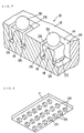
- FIG. 1 schematically shows a whole of an insulating housing 10 according to an embodiment of the present invention and FIG. 2 shows a partially enlarged view.
- the insulating housing 10 is formed of a suitable insulating material such as a liquid crystal polymer and a large number of openings 14 are opened in a predetermined pattern array in a top surface of the insulative housing.
- Projections 18, each, extend from a bottom wall 16 into the opening 14.
- a tapered end of the projection 18 is situated substantially flush with the top surface 12 of the insulating housing 10.
- Slots 20 are formed in positions adjacent both sides of the respective projection 18 and extend through the bottom wall 16. Through the slots 20 the opening 14 communicates with a bottom surface 22 of the insulative housing 10.
- preformed female terminals 24 each are detachably mounted on the projection 18 in the respective opening 14.
- the female terminal 24 in the present embodiment is formed like a clip and has a pair of plate-like spring arm sections 26 and a flat-plate-like base section 28 connecting these arm sections 26.
- the paired arms 26 pinch the projection 18 in a state contacting with the projection 18.
- the base section 28 is situated substantially parallel with the top surface 12 of the housing 10 and a solder ball 30 is attached on the base section 28 by a reflow soldering technique for example.
- the respective female terminal 24 is formed of a suitable terminal material such as phosphor bronze or beryllium copper.
- a tin-lead plated layer is formed at the female terminal's area on which the solder ball 30 is attached. It is preferable that a nickel underlaying gold-plated layer be formed at that portion of the female terminal with which the projection 18 is contacted.
- the female terminal 24 is comprised of a very simple structure having one pair of arms 26 and base section 28 and can be simply formed by one stamping operation.
- the insulative housing 10 having each female terminal 24 attached on the projection 18 with the solder ball 30 provides a female connector for providing a female connector on an IC package such as a CPU or a printed circuit board.
- each female terminal 24 is soldered to the IC package, by a reflow soldering method for instance, with the terminals 24 being arranged on the insulating housing 10.
- the openings 14 of the insulating housing 14 have their spacing, their size, etc., formed to match an array of electrodes exposed on the surface of the IC package.
- the respective female terminals have their solder balls 30 soldered to the associated electrodes of the IC package by the reflow soldering for instance and a resultant structure is formed as an IC package with the female connector integral therewith.
- FIG. 4 shows a state in which the female terminals 24 are mounted on an IC package P.
- the female terminals 24 are shown detached from the insulating housing 10. It is evident that, in order to protect the female terminals and IC package P, the insulating housing 10 is preferably retained in an mounted state until immediately before the female terminals are connected to an associated male connector.
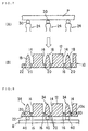
- FIGS. 5 and 6 show another insulative housing 10a formed such that it has the same structure as that of the above-mentioned housing 10.
- the same reference numerals are employed to designate parts or elements corresponding to those shown in the housing 10 and any further explanation is emitted for brevity.
- the insulating housing 10a constitutes a male connector. Respective projections 18 are formed as male terminals.
- a conductive layer 36 is directly plated to a plastic base, such as a liquid crystal polymer, and formed on an outer peripery of each projection 18, on an inner peripheral portion of the slot 20 adjacent the projection 18 and on a portion of the projection 18 corresponding to a bottom surface 22 of the housing, so that the conductive layer is electrically connected to the bottom surface 22 side.
- a nickel underlaying gold-plated layer is formed on the projection 18 side contacting with the above-mentioned female terminal 24.
- a tin-lead plated layer 39 is formed at a portion of the bottom surface 22 on a side opposite to that of the projection 18.
- a solder ball 40 constituting a contact section is attached on the tin-lead plated layer 39 by the reflow soldering technique for instance. By doing so, the solder ball 40 is electrically connected by the tin-lead plated layer 39 to the inside plated conductive layer 36 and by the conductive layer 36 to the plated contact layer 38 on the projection 18 side, the conductive layer 36 constituting a lead section.
- FIG. 6 shows a grid array of solder balls 40 attached on the bottom surface 22 side of the housing 10a.
- the thus formed insulating housing 10a constitutes a male connector where each male terminal 34 is arranged in an associated opening 14 and the solder balls 40 are projected from the bottom surface of the housing 10a.
- the male connector can be soldered by its solder balls 40 to the conductive pads of the printed circuit board, etc., with the use of, for example, the reflow soldering technique.
- FIGS. 7 and 8 show the IC package P with female terminals 24 mounted thereon and a printed circuit board B having the male connector with the insulating housing 10a.
- This IC package P is shipped such that, at a manufacture of the IC Package P, female terminals 24 and insulating housing 10 are mounted thereon.
- the insulating housing 10 is removed from the IC package P.
- FIG. 7(A) shows the IC package P with the insulating housing 10 detached
- FIG. 7(B) shows the insulating housing 10 detached from the IC package P.
- the insulating housing 10 is the same in structure as the insulating house 10a for forming the male connector on the printed circuit board B; the respective female terminals 24 attached on the projection 18 are aligned with the associated male terminals 34 formed on the projections 18, so that the male terminals 24 and female terminals 34 can be set in a positively engaged state without being misaligned from each other. Further, the respective female terminals 24 are transported in such a state as to be protected with the insulating housing 10. As a result, these female terminals 24 and IC package are not damaged during transportation.
- the insulative housing 10 and insulative housing 10a are the same in structure and it is not necessary to manufacture two types of housings in a separate fashion. It is, therefore, possible to manufacture both electric connectors, male and female, with the use of a single mold.
- an electric connector set comprised of the male and female connectors can be manufactured at low costs by the use of a pair of insulating housings having the same size and structure.
- the male connector and female connector it is possible to readily and positively connect together an IC package and printed circuit board having a large number of electrodes in a high density array.
- the male connector is such that the respective male terminal has a plated conductive layer formed on the circumference of the projection. Therefore, it is not necessary to attach any separate metal terminals, so that the male connector can be manufactured at low costs.
- the female connector is such that the female terminals are attached by the solder balls to the IC package or printed circuit board, it can be formed as a very compact unit. And the female terminals are attached to, and held in place in, the insulating housing the same as the insulating housing for the male terminals, so that it is possible to positively prevent any misalignment of the male terminals with the female terminals.
Abstract
Description
- The present invention relates to a high density electric connector, called as a BGA connector, connected to a board through solder balls arranged in a grid array.
- With a recent tendency of an electronic apparatus, such as a computer, toward a high density and miniaturization, a surface-mounting type high density connector called as a BGA connector has been developed in which a connection to a board is formed with solder balls such that the solder balls are arranged as a grid array on a housing. The BGA connector is positioned on contact pads arranged on a board surface. Then a resultant unit is heated to allow at least a portion of each terminal which is formed with the solder ball to be partially melted. By doing so, the solder ball is fused to the associated contact pad on the board. A distance between the adjoining solder ball terminals is very close and it is possible to provide a large number of connection portions on the board at a restricted area.
- In the case of a very compact, high-density connector for an IC package such as a CPU, it is very difficult to align each terminal relative to a large number of small electrodes arranged in a grid array. Thus a cumbersome operation is involved. Further, it is also difficult to align each terminal with respective terminals of a separately formed mating connector.
- It is accordingly the object of the present invention to provide very simple, inexpensive electrical connectors which can highly accurately align respective terminals of a pair of male and female connectors.
- In one aspect of the present invention, there is provided an electric connector set comprising: a pair of insulating housings having a plurality of openings arranged in an equal array and opened at a top surface, a plurality of projections extending from a bottom wall into the openings, and a plurality of slots extending through the bottom wall at those positions adjacent to the respective projections and allowing the bottom surface to communicate with the respective opening; female metal terminals detachably attached to the respective projections and each having a pair of arm sections and a base section connecting these arm sections to each other with a solder ball attached thereto, these female terminals being soldered by solder ball to one of an IC package and printed circuit board; male terminals having a contact section including a plated conductive layer formed on a peripheral portion of such projection of the other housing and engageable with the female terminal and a lead section including a plated conductive layer formed at those portions of the projection corresponding to the slot and housing bottom surface and electrically connected to the contact section; and the solder balls connected to the plated conductive layers of the housing bottom surface and soldered to the other of the IC package and printed circuit board.
- According to the electric connector set, the female terminals are soldered to one of the IC package and printed circuit board in a manner to be attached to the projections of one of the paired housing. When the housing is detached, the female terminals are exposed in a state to be protected from said one of the IC package and printed circuit board. Since, on the other hand, the male terminals are projected in the associated openings equal in array to the openings of the housing with the female terminals attached thereto, the male terminals and female terminals are positively located in their mutually aligned positions.
- In another aspect of the present invention, there is provided a male connector comprising: an insulating housing having a plurality of openings arranged in an equal array to an array of terminals of an associated female connector and opened at a top surface, a plurality of projections extending from a bottom wall into the corresponding opening, and a plurality of slots extending through the bottom wall at those positions adjacent to the projection and allowing the bottom surface to communicate with the opening; male terminals including a contact section having a plated conductive layer formed on a peripheral portion of the projection of the housing and engageable with the female terminal and a lead section including a plated conductive section formed at those portions of the projection corresponding to the slot and housing bottom surface and electrically connected to the contact section; and solder balls connected to the plated conductive layer on the housing bottom surface and soldered to the other of an IC package and printed circuit board. It is preferable that the contact section of the male terminal further have a plated contact layer on the conductive layer directly plated to the housing, the conductive layer containing gold.
- In another aspect of the present invention, there is provided a female connector forming set comprising: an insulating housing having a plurality of openings arranged in an equal array to terminals of a male connector and a plurality of projections extending form a bottom wall into the openings; female metal terminals detachably mounted on the projections and each having a pair of arm sections and a base section connecting these arm sections to each others; and solder balls attached to the base section of the respective female terminal and projected from a top surface of the housing, wherein, through these solder balls, respective female terminals are solderable to one of an IC package and printed circuit board.
- Since the female connector forming set has its female terminals detachably attached to the projections of the housing, it is soldered by the solder balls to the IC package or printed circuit board. When, thereafter, the housing is detached, the female connector is formed integral with the IC package or the printed circuit board.
- A method for manufacturing an electric connector, comprising the steps of: forming, at a pair of insulating housings, a plurality of openings arranged in an equal array and opened at a top surface, a plurality of projections extending from a bottom wall into the openings and a plurality of slots extending through a bottom wall at those positions adjacent to the respective projections and allowing the bottom surface to communicate with the respective opening; detachably attaching, to the respective projections of one of these housings, female metal terminals each having a pair of arm sections and a base section connecting together these arm sections with a solder ball attached on the base section; forming a continuous plated conductive layer on a peripheral portion of each projection of the other housing and on these portions of the projection corresponding to the slot and housing bottom surface and, by doing so, forming male terminals; connecting the solder ball to a plated conductive layer of the male terminal which is formed at the housing bottom surface; soldering the paired housings by the solder balls to an IC package and printed circuit, respectively, using a reflow soldering method; and detaching the one housing with the respective female terminals attached thereto from one of the IC package and printed circuit board and, by doing so, connecting together the IC package and printed circuit board.
-
- FIG. 1 is a perspective view diagrammatically showing an insulating housing for forming an electric connector set according to a preferred embodiment of the present invention;
- FIG. 2 is an explanatory view, partly enlarged, showing part of the insulating housing in FIG. 1;
- FIG. 3 is an explanatory view diagrammatically showing the insulating housing of FIG. 1 with female terminals and solder balls attached thereto;
- FIG. 4 is a perspective view diagrammatically showing an IC package with the female terminals attached thereto;
- FIG. 5 shows a male connector according to a preferred embodiment of the present invention, (A) in FIG. 5 generally showing a perspective view and (B) in FIG. 5 being a cross-sectional view, partly enlarged, showing the male terminal;
- FIG. 6 is a perspective view diagrammatically showing a state of the male connector as viewed from a solder ball side;
- FIG. 7 shows an IC package with the female terminals attached thereto, (A) in FIG. 7 being a side view diagrammatically showing an IC package immediately before being connected to the male connector after the insulating housing has been detached and (B) in FIG. 7 being a cross-sectional view showing the detached insulating housing; and
- FIG. 8 is a cross-sectional view showing a male connector attached to a printed circuit board.
-
- FIG. 1 schematically shows a whole of an
insulating housing 10 according to an embodiment of the present invention and FIG. 2 shows a partially enlarged view. - The insulating
housing 10 is formed of a suitable insulating material such as a liquid crystal polymer and a large number ofopenings 14 are opened in a predetermined pattern array in a top surface of the insulative housing.Projections 18, each, extend from abottom wall 16 into theopening 14. A tapered end of theprojection 18 is situated substantially flush with thetop surface 12 of theinsulating housing 10.Slots 20 are formed in positions adjacent both sides of therespective projection 18 and extend through thebottom wall 16. Through theslots 20 the opening 14 communicates with abottom surface 22 of theinsulative housing 10. - In the case where a female connector is to be formed, as shown in FIG. 3, preformed
female terminals 24 each are detachably mounted on theprojection 18 in therespective opening 14. Thefemale terminal 24 in the present embodiment is formed like a clip and has a pair of plate-likespring arm sections 26 and a flat-plate-like base section 28 connecting thesearm sections 26. The pairedarms 26 pinch theprojection 18 in a state contacting with theprojection 18. Further, thebase section 28 is situated substantially parallel with thetop surface 12 of thehousing 10 and asolder ball 30 is attached on thebase section 28 by a reflow soldering technique for example. - The respective
female terminal 24 is formed of a suitable terminal material such as phosphor bronze or beryllium copper. A tin-lead plated layer is formed at the female terminal's area on which thesolder ball 30 is attached. It is preferable that a nickel underlaying gold-plated layer be formed at that portion of the female terminal with which theprojection 18 is contacted. In the present embodiment, thefemale terminal 24 is comprised of a very simple structure having one pair ofarms 26 andbase section 28 and can be simply formed by one stamping operation. - The
insulative housing 10 having eachfemale terminal 24 attached on theprojection 18 with thesolder ball 30 provides a female connector for providing a female connector on an IC package such as a CPU or a printed circuit board. In the case where an electric connector of the CPU for example is to be formed, eachfemale terminal 24 is soldered to the IC package, by a reflow soldering method for instance, with theterminals 24 being arranged on theinsulating housing 10. In this case, in accordance with the array of the female terminals, theopenings 14 of theinsulating housing 14 have their spacing, their size, etc., formed to match an array of electrodes exposed on the surface of the IC package. The respective female terminals have theirsolder balls 30 soldered to the associated electrodes of the IC package by the reflow soldering for instance and a resultant structure is formed as an IC package with the female connector integral therewith. - FIG. 4 shows a state in which the
female terminals 24 are mounted on an IC package P. In FIG. 4, thefemale terminals 24 are shown detached from theinsulating housing 10. It is evident that, in order to protect the female terminals and IC package P, theinsulating housing 10 is preferably retained in an mounted state until immediately before the female terminals are connected to an associated male connector. - FIGS. 5 and 6 show another
insulative housing 10a formed such that it has the same structure as that of the above-mentionedhousing 10. In this housing, the same reference numerals are employed to designate parts or elements corresponding to those shown in thehousing 10 and any further explanation is emitted for brevity. - The
insulating housing 10a constitutes a male connector.Respective projections 18 are formed as male terminals. For this reason, as shown in (B) in FIG. 5, aconductive layer 36 is directly plated to a plastic base, such as a liquid crystal polymer, and formed on an outer peripery of eachprojection 18, on an inner peripheral portion of theslot 20 adjacent theprojection 18 and on a portion of theprojection 18 corresponding to abottom surface 22 of the housing, so that the conductive layer is electrically connected to thebottom surface 22 side. Further, a nickel underlaying gold-plated layer is formed on theprojection 18 side contacting with the above-mentionedfemale terminal 24. A tin-lead platedlayer 39 is formed at a portion of thebottom surface 22 on a side opposite to that of theprojection 18. Asolder ball 40 constituting a contact section is attached on the tin-lead platedlayer 39 by the reflow soldering technique for instance. By doing so, thesolder ball 40 is electrically connected by the tin-lead platedlayer 39 to the inside platedconductive layer 36 and by theconductive layer 36 to theplated contact layer 38 on theprojection 18 side, theconductive layer 36 constituting a lead section. FIG. 6 shows a grid array ofsolder balls 40 attached on thebottom surface 22 side of thehousing 10a. - The thus formed insulating
housing 10a constitutes a male connector where eachmale terminal 34 is arranged in an associatedopening 14 and thesolder balls 40 are projected from the bottom surface of thehousing 10a. The male connector can be soldered by itssolder balls 40 to the conductive pads of the printed circuit board, etc., with the use of, for example, the reflow soldering technique. - FIGS. 7 and 8 show the IC package P with
female terminals 24 mounted thereon and a printed circuit board B having the male connector with theinsulating housing 10a. This IC package P is shipped such that, at a manufacture of the IC Package P,female terminals 24 and insulatinghousing 10 are mounted thereon. When the IC package P is mounted on the printed circuit board B, the insulatinghousing 10 is removed from the IC package P. FIG. 7(A) shows the IC package P with the insulatinghousing 10 detached, and FIG. 7(B) shows the insulatinghousing 10 detached from the IC package P. Since the insulatinghousing 10 is the same in structure as the insulatinghouse 10a for forming the male connector on the printed circuit board B; the respectivefemale terminals 24 attached on theprojection 18 are aligned with the associatedmale terminals 34 formed on theprojections 18, so that themale terminals 24 andfemale terminals 34 can be set in a positively engaged state without being misaligned from each other. Further, the respectivefemale terminals 24 are transported in such a state as to be protected with the insulatinghousing 10. As a result, thesefemale terminals 24 and IC package are not damaged during transportation. - Further, the
insulative housing 10 andinsulative housing 10a are the same in structure and it is not necessary to manufacture two types of housings in a separate fashion. It is, therefore, possible to manufacture both electric connectors, male and female, with the use of a single mold. - As evident from the above, according to the present invention, an electric connector set comprised of the male and female connectors can be manufactured at low costs by the use of a pair of insulating housings having the same size and structure. Through the male connector and female connector, it is possible to readily and positively connect together an IC package and printed circuit board having a large number of electrodes in a high density array.
- The male connector is such that the respective male terminal has a plated conductive layer formed on the circumference of the projection. Therefore, it is not necessary to attach any separate metal terminals, so that the male connector can be manufactured at low costs.
- Since the female connector is such that the female terminals are attached by the solder balls to the IC package or printed circuit board, it can be formed as a very compact unit. And the female terminals are attached to, and held in place in, the insulating housing the same as the insulating housing for the male terminals, so that it is possible to positively prevent any misalignment of the male terminals with the female terminals.
Claims (5)
- An electric connector set comprising:a pair of insulating housings (10, 10a) having a plurality of openings (14) arranged in an equal array and opened at a top surface (12), a plurality of projections (18) extending from a bottom wall (16) into the openings (14), and a plurality of slots (20) extending through the bottom wall (16) at those positions adjacent to the respective projections (18) and allowing the bottom surface to communicate with the respective opening;female metal terminals (24) detachably attached to the respective projections (18) and each having a pair of arm sections (26) and a base section (28) connecting these arm sections (26) to each other with a solder ball (30) attached thereto, these female terminals (24) being soldered by solder balls (30) to one of an IC package and printed circuit board;male terminals (34) having a contact section (38) including a plated conductive layer formed on a peripheral portion of each projection (18) of the other housing (10a) and engageable with the female terminal (24) and a lead section (36) including a plated conductive layer formed at those portions of the projection corresponding to the slot and housing bottom surface (22) and electrically connected to the contact section (38); andthe solder balls (30) connected to the plated conductive layers of the housing bottom surface (22) and soldered to the other of the IC package and printed circuit board.
- A male connector comprising:an insulating housing (10a) having a plurality of openings (14) arranged in an equal array to an array of terminals of an associated female connector and opened at a top surface (12), a plurality of projections (18) extending from a bottom wall (16) into the corresponding opening (14), and a plurality of slots (20) extending through the bottom wall (16) at those positions adjacent to the projection (18) and allowing the bottom surface (22) to communicate with the opening (14);male terminals (34) including a contact section (38) having a plated conductive layer (36) formed on a peripheral portion of the projection (18) of the housing (10a) and engageable with the female terminal (24) and a lead section including a plated conductive section formed at those portions of the projection (18) corresponding to the slot (20) and housing bottom surface (22) and electrically connected to the contact section; andsolder balls (40) connected to the plated conductive layer (36) on the housing bottom surface (22) and soldered to the other of an IC package and printed circuit board.
- A male connector according to claim 2, wherein the contact section of the male terminal (34) further has a plated contact layer (39) on the conductive layer (36) directly plated to the housing (10a), the contact layer (39) containing gold.
- A female connector forming set comprising:an insulating housing (10) having a plurality of openings (14) arranged in an equal array to terminals of a male connector and a plurality of projections (18) extending from a bottom wall (16) into the openings (14);female metal terminals (24) detachably mounted on the projections (18) and each having a pair of arm sections (26) and a base section (28) connecting these arm sections (26) to each other; andsolder balls (40) attached to the base section (28) of the respective female terminal (24) and projected from a top surface (12) of the housing (10), wherein,
through these solder balls (40), respective female terminals (24) are solderable to one of an IC package and printed circuit board. - A method for manufacturing an electric connector, comprising the steps of:forming, at a pair of insulating housings (10, 10a), a plurality of openings (14) arranged in an equal array and opened at a top surface (12), a plurality of projections (18) extending from a bottom wall (16) into the openings (14) and a plurality of slots (20) extending through a bottom wall (16) at those positions adjacent to the respective projections (18) and allowing the bottom surface (22) to communicate with the respective opening (14);detachably attaching, to the respective projections (18) of one of these housings (10, 10a), female metal terminals (24) each having a pair of arm sections (26) and a base section (28) connecting together these arm sections (26) with a solder ball (40) attached on the base section,forming a continuous plated conductive layer (36) on a peripheral portion of each projection (18) of the other housing and on these portions of the projection (18) corresponding to the slot (20) and housing bottom surface (22) and, by doing so, forming male terminals (24);connecting the solder ball (40) to a plated conductive layer of the male terminal which is formed at the housing bottom surface (22);soldering the paired housings (10, 10a) by the solder balls (40) to an IC package and printed circuit, respectively, using a reflow soldering method; anddetaching said one housing with the respective female terminals (24) attached thereto from one of the IC package and printed circuit board and, by doing so, connecting together the IC package and printed circuit board.
Applications Claiming Priority (2)
| Application Number | Priority Date | Filing Date | Title |
|---|---|---|---|
| JP8147499 | 1999-03-25 | ||
| JP11081474A JP2000277885A (en) | 1999-03-25 | 1999-03-25 | Electrical connector and its manufacture |
Publications (3)
| Publication Number | Publication Date |
|---|---|
| EP1039542A2 true EP1039542A2 (en) | 2000-09-27 |
| EP1039542A3 EP1039542A3 (en) | 2001-03-14 |
| EP1039542B1 EP1039542B1 (en) | 2007-03-14 |
Family
ID=13747412
Family Applications (1)
| Application Number | Title | Priority Date | Filing Date |
|---|---|---|---|
| EP00105368A Expired - Lifetime EP1039542B1 (en) | 1999-03-25 | 2000-03-17 | Connector set |
Country Status (6)
| Country | Link |
|---|---|
| US (1) | US6328577B1 (en) |
| EP (1) | EP1039542B1 (en) |
| JP (1) | JP2000277885A (en) |
| AT (1) | ATE357073T1 (en) |
| DE (1) | DE60033880T2 (en) |
| SG (1) | SG86382A1 (en) |
Families Citing this family (7)
| Publication number | Priority date | Publication date | Assignee | Title |
|---|---|---|---|---|
| JP3741934B2 (en) * | 2000-05-10 | 2006-02-01 | シャープ株式会社 | Terminal connection device for flexible substrate |
| US6951596B2 (en) | 2002-01-18 | 2005-10-04 | Avery Dennison Corporation | RFID label technique |
| DE10257527A1 (en) * | 2002-12-10 | 2004-06-24 | Marquardt Gmbh | circuit support |
| US6979238B1 (en) * | 2004-06-28 | 2005-12-27 | Samtec, Inc. | Connector having improved contacts with fusible members |
| US7371131B2 (en) * | 2005-04-04 | 2008-05-13 | Fci Americas Technology, Inc. | Connector having retentive rib |
| US7623034B2 (en) | 2005-04-25 | 2009-11-24 | Avery Dennison Corporation | High-speed RFID circuit placement method and device |
| US8183155B1 (en) * | 2011-03-30 | 2012-05-22 | Hon Hai Precision Ind. Co., Ltd. | Lower profile connector assembly |
Citations (4)
| Publication number | Priority date | Publication date | Assignee | Title |
|---|---|---|---|---|
| US5702255A (en) * | 1995-11-03 | 1997-12-30 | Advanced Interconnections Corporation | Ball grid array socket assembly |
| EP0836243A2 (en) * | 1996-10-10 | 1998-04-15 | Berg Electronics Manufacturing B.V. | High density connector and method of manufacture |
| US5746608A (en) * | 1995-11-30 | 1998-05-05 | Taylor; Attalee S. | Surface mount socket for an electronic package, and contact for use therewith |
| GB2325354A (en) * | 1997-03-26 | 1998-11-18 | Whitaker Corp | Electrical connector or connection with concave ball-receiving site |
Family Cites Families (5)
| Publication number | Priority date | Publication date | Assignee | Title |
|---|---|---|---|---|
| US5772451A (en) | 1993-11-16 | 1998-06-30 | Form Factor, Inc. | Sockets for electronic components and methods of connecting to electronic components |
| US5593322A (en) | 1995-01-17 | 1997-01-14 | Dell Usa, L.P. | Leadless high density connector |
| US5730606A (en) | 1996-04-02 | 1998-03-24 | Aries Electronics, Inc. | Universal production ball grid array socket |
| US6024584A (en) * | 1996-10-10 | 2000-02-15 | Berg Technology, Inc. | High density connector |
| US5876219A (en) * | 1997-08-29 | 1999-03-02 | The Whitaker Corp. | Board-to-board connector assembly |
-
1999
- 1999-03-25 JP JP11081474A patent/JP2000277885A/en not_active Withdrawn
-
2000
- 2000-03-15 SG SG200001510A patent/SG86382A1/en unknown
- 2000-03-17 EP EP00105368A patent/EP1039542B1/en not_active Expired - Lifetime
- 2000-03-17 DE DE60033880T patent/DE60033880T2/en not_active Expired - Fee Related
- 2000-03-17 AT AT00105368T patent/ATE357073T1/en not_active IP Right Cessation
- 2000-03-22 US US09/532,548 patent/US6328577B1/en not_active Expired - Fee Related
Patent Citations (4)
| Publication number | Priority date | Publication date | Assignee | Title |
|---|---|---|---|---|
| US5702255A (en) * | 1995-11-03 | 1997-12-30 | Advanced Interconnections Corporation | Ball grid array socket assembly |
| US5746608A (en) * | 1995-11-30 | 1998-05-05 | Taylor; Attalee S. | Surface mount socket for an electronic package, and contact for use therewith |
| EP0836243A2 (en) * | 1996-10-10 | 1998-04-15 | Berg Electronics Manufacturing B.V. | High density connector and method of manufacture |
| GB2325354A (en) * | 1997-03-26 | 1998-11-18 | Whitaker Corp | Electrical connector or connection with concave ball-receiving site |
Also Published As
| Publication number | Publication date |
|---|---|
| US6328577B1 (en) | 2001-12-11 |
| SG86382A1 (en) | 2002-02-19 |
| DE60033880T2 (en) | 2007-12-06 |
| JP2000277885A (en) | 2000-10-06 |
| EP1039542A3 (en) | 2001-03-14 |
| ATE357073T1 (en) | 2007-04-15 |
| DE60033880D1 (en) | 2007-04-26 |
| EP1039542B1 (en) | 2007-03-14 |
Similar Documents
| Publication | Publication Date | Title |
|---|---|---|
| JP4782740B2 (en) | Low profile connector | |
| US6733303B2 (en) | Low pitch, high density connector | |
| EP0657960B1 (en) | Printed circuit board connector | |
| US6398559B2 (en) | Connecting terminal and a connecting terminal assembly | |
| US6155848A (en) | Auxiliary device for ZIF electrical connector | |
| JP2555593Y2 (en) | Surface mount type connector | |
| EP1049202B1 (en) | Electrical connector | |
| US7413450B2 (en) | Printed circuit board assembly having a BGA connection | |
| US6176743B1 (en) | Electrical adapter | |
| US6666693B2 (en) | Surface-mounted right-angle electrical connector | |
| US6533610B1 (en) | Low-profile RF connector assembly | |
| US6623284B1 (en) | Electrical connector | |
| US20050124198A1 (en) | Socket connector for integrated circuit | |
| US6116923A (en) | Electrical connector | |
| US20050009385A1 (en) | Electrical connector having improved contacts | |
| EP1039542B1 (en) | Connector set | |
| US20100317232A1 (en) | Low profile socket connector and method for making the same | |
| US7841859B2 (en) | Socket with solder pad | |
| US6638082B2 (en) | Pin-grid-array electrical connector | |
| US20050064745A1 (en) | Terminal for electrical connector | |
| JP3436491B2 (en) | Board surface mount connector | |
| US6644983B2 (en) | Contact assembly, connector assembly utilizing same, and electronic assembly | |
| JP2531600Y2 (en) | Board connection connector | |
| US11735849B2 (en) | Electrical connector manufacturing method | |
| KR100675703B1 (en) | Connector set |
Legal Events
| Date | Code | Title | Description |
|---|---|---|---|
| PUAI | Public reference made under article 153(3) epc to a published international application that has entered the european phase |
Free format text: ORIGINAL CODE: 0009012 |
|
| AK | Designated contracting states |
Kind code of ref document: A2 Designated state(s): AT BE CH CY DE DK ES FI FR GB GR IE IT LI LU MC NL PT SE |
|
| AX | Request for extension of the european patent |
Free format text: AL;LT;LV;MK;RO;SI |
|
| PUAL | Search report despatched |
Free format text: ORIGINAL CODE: 0009013 |
|
| AK | Designated contracting states |
Kind code of ref document: A3 Designated state(s): AT BE CH CY DE DK ES FI FR GB GR IE IT LI LU MC NL PT SE |
|
| AX | Request for extension of the european patent |
Free format text: AL;LT;LV;MK;RO;SI |
|
| RIC1 | Information provided on ipc code assigned before grant |
Free format text: 7H 01R 43/02 A, 7H 05K 3/34 B, 7H 01L 23/498 B, 7H 05K 7/10 B |
|
| 17P | Request for examination filed |
Effective date: 20010903 |
|
| AKX | Designation fees paid |
Free format text: AT BE CH CY DE DK ES FI FR GB GR IE IT LI LU MC NL PT SE |
|
| GRAP | Despatch of communication of intention to grant a patent |
Free format text: ORIGINAL CODE: EPIDOSNIGR1 |
|
| GRAS | Grant fee paid |
Free format text: ORIGINAL CODE: EPIDOSNIGR3 |
|
| GRAA | (expected) grant |
Free format text: ORIGINAL CODE: 0009210 |
|
| RAP1 | Party data changed (applicant data changed or rights of an application transferred) |
Owner name: FCI |
|
| AK | Designated contracting states |
Kind code of ref document: B1 Designated state(s): AT BE CH CY DE DK ES FI FR GB GR IE IT LI LU MC NL PT SE |
|
| PG25 | Lapsed in a contracting state [announced via postgrant information from national office to epo] |
Ref country code: LI Free format text: LAPSE BECAUSE OF FAILURE TO SUBMIT A TRANSLATION OF THE DESCRIPTION OR TO PAY THE FEE WITHIN THE PRESCRIBED TIME-LIMIT Effective date: 20070314 Ref country code: BE Free format text: LAPSE BECAUSE OF FAILURE TO SUBMIT A TRANSLATION OF THE DESCRIPTION OR TO PAY THE FEE WITHIN THE PRESCRIBED TIME-LIMIT Effective date: 20070314 Ref country code: FI Free format text: LAPSE BECAUSE OF FAILURE TO SUBMIT A TRANSLATION OF THE DESCRIPTION OR TO PAY THE FEE WITHIN THE PRESCRIBED TIME-LIMIT Effective date: 20070314 Ref country code: NL Free format text: LAPSE BECAUSE OF FAILURE TO SUBMIT A TRANSLATION OF THE DESCRIPTION OR TO PAY THE FEE WITHIN THE PRESCRIBED TIME-LIMIT Effective date: 20070314 Ref country code: CH Free format text: LAPSE BECAUSE OF FAILURE TO SUBMIT A TRANSLATION OF THE DESCRIPTION OR TO PAY THE FEE WITHIN THE PRESCRIBED TIME-LIMIT Effective date: 20070314 Ref country code: AT Free format text: LAPSE BECAUSE OF FAILURE TO SUBMIT A TRANSLATION OF THE DESCRIPTION OR TO PAY THE FEE WITHIN THE PRESCRIBED TIME-LIMIT Effective date: 20070314 |
|
| REG | Reference to a national code |
Ref country code: GB Ref legal event code: FG4D |
|
| REG | Reference to a national code |
Ref country code: CH Ref legal event code: EP |
|
| REF | Corresponds to: |
Ref document number: 60033880 Country of ref document: DE Date of ref document: 20070426 Kind code of ref document: P |
|
| REG | Reference to a national code |
Ref country code: IE Ref legal event code: FG4D |
|
| PG25 | Lapsed in a contracting state [announced via postgrant information from national office to epo] |
Ref country code: SE Free format text: LAPSE BECAUSE OF FAILURE TO SUBMIT A TRANSLATION OF THE DESCRIPTION OR TO PAY THE FEE WITHIN THE PRESCRIBED TIME-LIMIT Effective date: 20070614 |
|
| PG25 | Lapsed in a contracting state [announced via postgrant information from national office to epo] |
Ref country code: ES Free format text: LAPSE BECAUSE OF FAILURE TO SUBMIT A TRANSLATION OF THE DESCRIPTION OR TO PAY THE FEE WITHIN THE PRESCRIBED TIME-LIMIT Effective date: 20070625 |
|
| ET | Fr: translation filed | ||
| PG25 | Lapsed in a contracting state [announced via postgrant information from national office to epo] |
Ref country code: PT Free format text: LAPSE BECAUSE OF FAILURE TO SUBMIT A TRANSLATION OF THE DESCRIPTION OR TO PAY THE FEE WITHIN THE PRESCRIBED TIME-LIMIT Effective date: 20070814 |
|
| NLV1 | Nl: lapsed or annulled due to failure to fulfill the requirements of art. 29p and 29m of the patents act | ||
| REG | Reference to a national code |
Ref country code: CH Ref legal event code: PL |
|
| PLBE | No opposition filed within time limit |
Free format text: ORIGINAL CODE: 0009261 |
|
| STAA | Information on the status of an ep patent application or granted ep patent |
Free format text: STATUS: NO OPPOSITION FILED WITHIN TIME LIMIT |
|
| PG25 | Lapsed in a contracting state [announced via postgrant information from national office to epo] |
Ref country code: MC Free format text: LAPSE BECAUSE OF NON-PAYMENT OF DUE FEES Effective date: 20070331 Ref country code: DK Free format text: LAPSE BECAUSE OF FAILURE TO SUBMIT A TRANSLATION OF THE DESCRIPTION OR TO PAY THE FEE WITHIN THE PRESCRIBED TIME-LIMIT Effective date: 20070314 Ref country code: IE Free format text: LAPSE BECAUSE OF NON-PAYMENT OF DUE FEES Effective date: 20070320 |
|
| 26N | No opposition filed |
Effective date: 20071217 |
|
| PG25 | Lapsed in a contracting state [announced via postgrant information from national office to epo] |
Ref country code: IT Free format text: LAPSE BECAUSE OF FAILURE TO SUBMIT A TRANSLATION OF THE DESCRIPTION OR TO PAY THE FEE WITHIN THE PRESCRIBED TIME-LIMIT Effective date: 20070314 Ref country code: GR Free format text: LAPSE BECAUSE OF FAILURE TO SUBMIT A TRANSLATION OF THE DESCRIPTION OR TO PAY THE FEE WITHIN THE PRESCRIBED TIME-LIMIT Effective date: 20070615 |
|
| PGFP | Annual fee paid to national office [announced via postgrant information from national office to epo] |
Ref country code: GB Payment date: 20080211 Year of fee payment: 9 |
|
| PGFP | Annual fee paid to national office [announced via postgrant information from national office to epo] |
Ref country code: DE Payment date: 20080331 Year of fee payment: 9 Ref country code: FR Payment date: 20080307 Year of fee payment: 9 |
|
| PG25 | Lapsed in a contracting state [announced via postgrant information from national office to epo] |
Ref country code: CY Free format text: LAPSE BECAUSE OF FAILURE TO SUBMIT A TRANSLATION OF THE DESCRIPTION OR TO PAY THE FEE WITHIN THE PRESCRIBED TIME-LIMIT Effective date: 20070314 |
|
| PG25 | Lapsed in a contracting state [announced via postgrant information from national office to epo] |
Ref country code: LU Free format text: LAPSE BECAUSE OF NON-PAYMENT OF DUE FEES Effective date: 20070317 |
|
| GBPC | Gb: european patent ceased through non-payment of renewal fee |
Effective date: 20090317 |
|
| REG | Reference to a national code |
Ref country code: FR Ref legal event code: ST Effective date: 20091130 |
|
| PG25 | Lapsed in a contracting state [announced via postgrant information from national office to epo] |
Ref country code: DE Free format text: LAPSE BECAUSE OF NON-PAYMENT OF DUE FEES Effective date: 20091001 |
|
| PG25 | Lapsed in a contracting state [announced via postgrant information from national office to epo] |
Ref country code: GB Free format text: LAPSE BECAUSE OF NON-PAYMENT OF DUE FEES Effective date: 20090317 Ref country code: FR Free format text: LAPSE BECAUSE OF NON-PAYMENT OF DUE FEES Effective date: 20091123 |