EP1055903A1 - Optical techniques for measuring layer thicknesses and other surface characteristics of objects such as semiconductor wafers - Google Patents
Optical techniques for measuring layer thicknesses and other surface characteristics of objects such as semiconductor wafers Download PDFInfo
- Publication number
- EP1055903A1 EP1055903A1 EP00304118A EP00304118A EP1055903A1 EP 1055903 A1 EP1055903 A1 EP 1055903A1 EP 00304118 A EP00304118 A EP 00304118A EP 00304118 A EP00304118 A EP 00304118A EP 1055903 A1 EP1055903 A1 EP 1055903A1
- Authority
- EP
- European Patent Office
- Prior art keywords
- radiation
- optical radiation
- optical
- layer
- thickness
- Prior art date
- Legal status (The legal status is an assumption and is not a legal conclusion. Google has not performed a legal analysis and makes no representation as to the accuracy of the status listed.)
- Granted
Links
Images


Classifications
-
- B—PERFORMING OPERATIONS; TRANSPORTING
- B24—GRINDING; POLISHING
- B24B—MACHINES, DEVICES, OR PROCESSES FOR GRINDING OR POLISHING; DRESSING OR CONDITIONING OF ABRADING SURFACES; FEEDING OF GRINDING, POLISHING, OR LAPPING AGENTS
- B24B37/00—Lapping machines or devices; Accessories
- B24B37/005—Control means for lapping machines or devices
- B24B37/013—Devices or means for detecting lapping completion
-
- B—PERFORMING OPERATIONS; TRANSPORTING
- B24—GRINDING; POLISHING
- B24B—MACHINES, DEVICES, OR PROCESSES FOR GRINDING OR POLISHING; DRESSING OR CONDITIONING OF ABRADING SURFACES; FEEDING OF GRINDING, POLISHING, OR LAPPING AGENTS
- B24B49/00—Measuring or gauging equipment for controlling the feed movement of the grinding tool or work; Arrangements of indicating or measuring equipment, e.g. for indicating the start of the grinding operation
- B24B49/02—Measuring or gauging equipment for controlling the feed movement of the grinding tool or work; Arrangements of indicating or measuring equipment, e.g. for indicating the start of the grinding operation according to the instantaneous size and required size of the workpiece acted upon, the measuring or gauging being continuous or intermittent
- B24B49/04—Measuring or gauging equipment for controlling the feed movement of the grinding tool or work; Arrangements of indicating or measuring equipment, e.g. for indicating the start of the grinding operation according to the instantaneous size and required size of the workpiece acted upon, the measuring or gauging being continuous or intermittent involving measurement of the workpiece at the place of grinding during grinding operation
-
- B—PERFORMING OPERATIONS; TRANSPORTING
- B24—GRINDING; POLISHING
- B24B—MACHINES, DEVICES, OR PROCESSES FOR GRINDING OR POLISHING; DRESSING OR CONDITIONING OF ABRADING SURFACES; FEEDING OF GRINDING, POLISHING, OR LAPPING AGENTS
- B24B49/00—Measuring or gauging equipment for controlling the feed movement of the grinding tool or work; Arrangements of indicating or measuring equipment, e.g. for indicating the start of the grinding operation
- B24B49/12—Measuring or gauging equipment for controlling the feed movement of the grinding tool or work; Arrangements of indicating or measuring equipment, e.g. for indicating the start of the grinding operation involving optical means
-
- G—PHYSICS
- G01—MEASURING; TESTING
- G01B—MEASURING LENGTH, THICKNESS OR SIMILAR LINEAR DIMENSIONS; MEASURING ANGLES; MEASURING AREAS; MEASURING IRREGULARITIES OF SURFACES OR CONTOURS
- G01B11/00—Measuring arrangements characterised by the use of optical techniques
- G01B11/02—Measuring arrangements characterised by the use of optical techniques for measuring length, width or thickness
- G01B11/06—Measuring arrangements characterised by the use of optical techniques for measuring length, width or thickness for measuring thickness ; e.g. of sheet material
- G01B11/0616—Measuring arrangements characterised by the use of optical techniques for measuring length, width or thickness for measuring thickness ; e.g. of sheet material of coating
- G01B11/0625—Measuring arrangements characterised by the use of optical techniques for measuring length, width or thickness for measuring thickness ; e.g. of sheet material of coating with measurement of absorption or reflection
-
- G—PHYSICS
- G01—MEASURING; TESTING
- G01N—INVESTIGATING OR ANALYSING MATERIALS BY DETERMINING THEIR CHEMICAL OR PHYSICAL PROPERTIES
- G01N21/00—Investigating or analysing materials by the use of optical means, i.e. using sub-millimetre waves, infrared, visible or ultraviolet light
- G01N21/17—Systems in which incident light is modified in accordance with the properties of the material investigated
- G01N21/47—Scattering, i.e. diffuse reflection
- G01N21/4738—Diffuse reflection, e.g. also for testing fluids, fibrous materials
Definitions
- This invention relates generally to techniques for determining conditions of surfaces, and, more specifically, to doing so by measuring a characteristic of the reflectivity and/or emissivity of surfaces.
- An example application is the measurement of the thickness of a film on a substrate, such as a film that is formed or removed from a semiconductor wafer during the fabrication of integrated circuits. The thickness measurement is made either simultaneously with the film processing (in situ) or thereafter (in line). More specific applications include in situ measurements of the thickness of a film being reduced or removed by techniques such as wet etching, plasma etching, spin etching or chemical-mechanical-polishing (CMP).
- CMP chemical-mechanical-polishing
- 5,695,660 measures the thickness or level of planarization of both dielectric and metal layers in situ by optical or thermal techniques during etching or CMP, including making the measurements through the back side of the wafer.
- CMP chemical vapor deposition
- an optical signal communicates with a wafer being processed through an optical window provided in one of the moving elements such as the wafer carrier.
- PCT published international
- WO 97/25660 multiple sensors are carried by a moving component of a CMP machine, with a wireless communication of measurements and control signals provided between the sensors and a host control station.
- Other patent documents of interest include U.S. patents nos.
- a surface being monitored is illuminated by optical radiation with rays of the incident radiation spread over a wide angle to form a radiation field modified by the surface that is also collected over a wide angle and detected by a sensor.
- the angles of optical radiation illumination and collection are made sufficiently wide so that variations in an optical radiation path and/or of the surface being monitored, other than of the surface optical characteristic of interest, that occur over time or between different copies of the surface are minimized or substantially eliminated in order to improve the accuracy of the resultant measurements.
- the incident radiation is preferably spread over an angle of at least 45 degrees and up to 180 degrees when striking the surface being monitored, and is also preferably collected over an angle of 45 degrees or more, and up to 180 degrees. As the illumination angle is increased, the collection angle can be made narrower.
- the collected radiation is detected, and the detected radiation is processed to monitor a desired characteristic of the surface.
- Specific structures of sensors include use of an optical radiation spreading element, such as a diffuser or multi-pass reflector, positioned near to the surface being monitored, and an optical collection element, such as an end of an optical fiber or a lens, is positioned to receive the spread radiation after being modified by the surface, such as by reflection from the surface. Random or pseudo-random scattering of the illumination radiation is preferred, such as occurs when the optical radiation incident on the surface being monitored has passed through ground glass.
- the wide angle illumination and detection significantly reduces the effects of variations in scattering of the optical signals that can occur independently of the quantity desired to be measured.
- the incident optical radiation, and that modified by the surface being monitored can be scattered varying amounts that depend upon the surface, angles that the radiation strikes the surface and optical elements, changes over time, and other causes. If narrow angles are viewed, for example, any variation in the amount of incident radiation that is scatted into the narrow viewing angle because of differences in scattering properties across the surface being monitored or between different surfaces, versus that which is scattered over wider angles out of view, causes the detected optical signal to vary. Significant variations can also occur when the surface is being viewed through a liquid layer, such as an etchant or slurry, that changes its thickness and other characteristics over time.
- optical radiation is used in this application to mean electromagnetic radiation in a continuous wavelength range including visible and near visible infrared and ultraviolet wavelengths, generally considered to extend from about 0.2 to about 4 microns.
- Monitoring the optical radiation modified by a surface usually also includes monitoring the level of radiation incident upon the surface so that the reflectivity or emissivity of the surface, or a related quantity, can be calculated either as the ultimate surface characteristic to be determined or as an intermediate quantity used to calculate some other surface characteristic.
- resulting calculations of the reflectivity or emissivity of the surface are highly meaningful because they are independent of changing conditions unrelated to surface reflectivity and emissivity.
- the calculation of emissivity is preferred because it is understood in the scientific community to be independent of the geometry, wavelength and other factors that can cause undesired variations in optical measurements.
- a layer of material being formed on or removed from a substrate, in whole or in part, is being monitored, it is preferably illuminated and viewed in the above described manner.
- An endpoint to the complete removal of a layer is one characteristic of the surface that may be determined.
- Another characteristic is the thickness of the layer, either in relative or absolute terms. Because surface reflectivity or emissivity is being determined with the effects of varying measurement conditions being minimized, the thickness of a layer can be determined with a high degree of accuracy by a look-up table, model or other relationship between the reflectivity or emissivity and thickness.
- the monitored layer is a metal or other generally opaque material
- its reflectivity and emissivity are directly related to the thickness of the layer if the layer is thin enough to be at least partially transparent.
- the layer's reflectivity or emissivity when measured by the techniques summarized above, is directly related to the thickness of the metal layer once it has become thin enough to be semi-transparent.
- a metal film on a semiconductor wafer is semi-transparent when its thickness is less than about 500 to 1500 Angstroms, depending on the metal and the wavelength of radiation used. Therefore, for such thin metal layers, their thicknesses can be determined from a look-up table or set of functions that relate the measured reflectivity or emissivity with the layer's thickness.
- the optical properties being measured are those of the layers under the metal film.
- the measurement of the reflectivity or emissivity of a metal layer can be conducted with one or more wavelengths of optical radiation.
- the thickness of a layer of transparent material can be monitored throughout a range of its entire thickness by viewing a signal resulting from interference of a portion of the incident optical radiation reflected from an outside surface from which material is being removed and another portion of the incident radiation reflected from some other interface in the structure of the substrate and layer.
- a given table or set of functions are used to relate specific values of the interference signal with layer thicknesses.
- Interference signals are preferably generated in at least two different wavelengths of optical radiation. Precise measurements of the thickness of a transparent layer are then obtainable without ambiguity under many circumstances when the two or more optical radiation wavelengths and ranges of layer thicknesses are suitable. In other cases, such precision additionally requires knowledge of the approximate layer thickness, as determined by observation or otherwise, in order to obtain a precise measurement of the transparent layer's thickness without ambiguity.
- the radiation can be generated by separate narrow bandwidth radiation sources, such as light emitting diodes (LEDs), and then the uniquely responsive to one of the source wavelengths.
- the two or more radiation sources are each modulated with a unique frequency.
- Electrical signals obtained from a single or multiple radiation receiving photodetectors are then filtered to pass the source modulating frequencies in order to obtain a separate signal for each of the illumination wavelengths.
- the frequencies of modulation are preferably selected to be different from that of any ambient radiation or electrical noise that might be present in the environment in which the measurements are being taken, thereby to significantly reduce adverse effects of any such ambient radiation and noise.
- the radiation source modulation and photodetector signal filtering technique can also be used when a single optical radiation is directed at the surface being monitored in order to similarly reduce the effects of any ambient radiation and electrical noise that might be present at different frequencies from the modulating frequency.
- CMP CMP
- substrates such as semiconductor wafers
- a slurry of abrasive particles and a chemical etchant is usually also used on the pad.
- One or more optical radiation sensors are installed in either the carrier, if the processing is being viewed from the back side of the substrates, or in the platen, if being viewed from the front side of the substrates.
- the front side of the wafers can also be periodically viewed in some CMP machines when the wafers are being loaded into or unloaded from the CMP machine, or are periodically moved off the platen within the CMP machine during the CMP process.
- An analog signal obtained from a sensor installed in a CMP machine platen is a continuous one, resulting from being scanned across the one or more wafers held by the carrier and the surface of the carrier in between the wafers. If the reflectivity and emissivity of the carrier surface is significantly different than that of the wafers, there is a significant discontinuity of the signal obtained by the photodetector as its view crosses an edge of the wafer. Discrete measurements of the wafer surface are referenced to these discontinuities as a way of identifying the positions of the measurements. In some cases it is desired to take specific measurements near an edge of the wafer outside of patterned circuit die, and in others it is desired to take specific measurements over a patterned location. Control of the location is made possible by use of the edge discontinuity. The measurements at specific positions of the wafers are then monitored over time in order to measure the effect of the processing on the wafer surface.
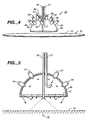
- a substrate or other object 11 contains a surface 13 that is being measured.
- An optical sensor head 15 directs optical radiation from one or more light emitting diodes (LEDs) against a spot 17 of the surface 13.
- LEDs light emitting diodes
- Other sources of optical radiation can be used instead of LEDs but it is preferred that they have a narrow bandwidth, such as a few dozen nanometers in wavelength, or less. Highly coherent sources of optical radiation are unnecessary.
- a portion of the source radiation that is reflected from the surface is gathered by suitable optics, such as an optical fiber 19.
- Other optics, such as an optical fiber 21 collects a portion of the source radiation, preferably without any significant amount of radiation reflected from the surface, as background radiation that is used as a reference.
- the sensor head 15 is connected with a module 23 that includes optical and electronic elements to interface between the sensor 15 and a host controller 25, such as a personal computer.
- Photodetectors 27 and 29 receive the optical signals from the optical fibers 19 and 21, respectively, to generate electrical signals in respective lines 31 and 33. These electrical signals are amplified by respective amplifiers 35 and 37, whose outputs are connected with an analog-to-digital converter 39. The amplified and digitized outputs of the photodetectors 27 and 29 and then sent to a controller 41 which controls operation of the sensor 15 and of the module 23, and can make a portion or all of the calculations necessary to determine the ultimate quantity related to the characteristic of the surface 13 that is being measured.
- the module 23 also includes a power circuit 43 that supplies, through a line 45, the LEDs or other optical radiation source included within the sensor head 15.
- the power is supplied by the host controller 25 but controlled by the controller 41, the module 23 is preferably provided in a small rugged package so that it may be positioned near the head 15 in a piece of processing machinery.
- the size of the illuminated spot 17 is made to suit the measurement, a range of one-quarter to three-fourths of an inch in diameter for the applications specifically described herein.
- a diameter of the sensor head 15 of about one-half of one inch is preferred for the CMP applications described below, resulting in a spot 17 having a diameter something less than that, depending upon the optical elements at the end of the head 15.
- the size of the spot 17, of course, determines the area of the surface 13 that is averaged or integrated during each measurement.
- Measurements can be made at a single point of the surface 13, at multiple points, or continuously across the surface 13, such as along a path 47, by providing relative motion between the head 15 and surface 13. Either the head 15 can be moved, or the substrate 11 moved, or both. In the CMP application described below, both are moved.
- Figure 2 shows a conceptual cross-sectional view of an end portion of the sensor head 15.
- Optical radiation from the source(s) (not shown in Figures 2 and 3) contained in the head 15 is directed through an optical radiation spreading element that extends across an end opening of a cylindrical housing 51.
- the element 49 spreads the source radiation over a maximum angle ⁇ , preferably with substantially uniform intensity.
- a diffraction element may be made for this purpose but use of ground glass for the element 49 operates satisfactorily and provides a randomness to the surface illumination. As discussed above, better results are obtained as the angle ⁇ increases.
- the element 49 is designed to provide this angle to be at least 45 degrees.
- An end of an optical fiber has an acceptance angle of optical radiation that depends primarily upon the refractive index of the fiber core material.
- Such an angle ⁇ is shown on Figure 2 at an end of the optical fiber 19, which extends through the element 49 to have an unobstructed view of the surface 13. It is also desirable that this angle be made as large as is practical, as discussed above, preferably 45 degrees or more.
- An optical fiber with a core made of sapphire, quartz or cubic zirconia has an angle of acceptance of about 45 degrees.
- a lens element 53 can be added to the end of the optical fiber 19, as shown in Figure 3.
- the diameter of the area viewed by the optical fiber 19 is increased, as indicated in Figure 3. It is the area of the surface 13 within the angle of acceptance ⁇ that defines the spot 17, assuming that this area is also substantially uniformly illuminated.
- FIG. 4 and 5 One specific embodiment of a sensor head 15 is shown in Figures 4 and 5, where elements that are counterparts of those described above are identified by the same reference numbers but, when different in structure, have a prime (') added to the reference number.
- a plurality of LEDs 55-64 are distributed around a hemispherical shell 65.
- a transparent cover 67 may be provided with radiation scattering properties but a wide distribution of radiation results from the numerous LEDs and internal reflection within the shell 65.
- the surface 13 is illuminated with a range of angles close to 180 degrees, depending upon the distance between the shell and the surface 13. Lenses provided as part of the LEDs may also be roughened to add to the diffusion of the illumination provided by the head 15 of Figures 4 and 5.
- FIG. 6 Another specific embodiment of a sensor head 15, which is preferred, is shown in cross section in Figure 6.
- a plurality of LEDs including LEDs 71 and 73, carried by a flat plate extending across the inside of the shell. Radiation from the LEDs passes through a diffuser 77 through which the radiation gathering optical fiber 19 extends, similar to the structure of Figures 2 and 3.
- the sensor head 15'' is sealed against liquids, moisture and gas vapors. This can be done at one end by sealing the diffuser 77 to the diffuser 77 but a better seal is obtained by adding a single piece clear glass plate 79 which extends completely across and is sealed to the inside of the shell 51.
- Optical radiation from the LEDs is gathered into the optical fiber 17 by positioning a circular diffusive reflecting element 81 around the optical fiber 19.
- the element 81 is made small enough so as not to block the diffuser 77 from receiving almost all of the radiation from the LEDs but large enough to reflect enough of the radiation into the optical fiber 17 to obtain a useful background reference signal.
- the wavelength of the optical radiation source is chosen to be the best for monitoring the particular surface characteristics of interest.
- the radiation needs to interact with the feature or characteristic of the object or its surface that is desired to be monitored, in a way that can be detected in the radiation after being modified by the object.
- wavelengths slightly below the band edge of silicon are usually best, generally infra-red radiation less than one micron, to which the wafer is opaque. If radiation is transmitted through the object being monitored to obtain an object modified beam that is detected, the radiation is, of course, chosen to be of a wavelength that will pass through the object.
- the controller 41 calculates a ratio of the reflected radiation signal from the photodetector 27 to the background radiation signal from the photodetector 29, as is well known.
- the instrument is first calibrated by positioning the sensor head 15 against at least one surface having a known reflectivity, and preferably against several surfaces having known different reflectivities. Calibration includes adjusting the relative gains of the two signal channels until the instrument reads the known reflectivity of the test surface. This is preferably done by software within the controller 41, particularly when multiple test surfaces are used.
- emissivity of a surface is calculated as a measure of the thickness of a layer of material that forms that surface.
- the primary application is in semiconductor processing but the techniques are not so limited.
- a changing thickness of a dielectric material which is transparent to the incident radiation, is monitored by measuring the interference of the radiation reflected from both surfaces of the layer. The interference signal passes through peaks and valleys as the layer either becomes thicker when being formed by chemical vapor deposition (CVD) or otherwise, or becomes thinner as material is removed by wet or dry etching, CMP or some other technique.
- FIG. 7 shows a modification of the single wavelength embodiments described above.
- Two different types of LEDs 91 and 92 emit optical radiation at wavelengths ⁇ 1 and ⁇ 2, respectively. This is reflected off the surface 13 and gathered by an optical fiber 93, passed to a beam splitter 95 and thence to photodetectors 97 and 99 through respective optical bandpass filters 101 ( ⁇ 1) and 103 ( ⁇ 2). The signal outputs of these photodetectors are then digitized by the analog-to-digital converter 39'.
- the reference radiation is obtained by an optical fiber 105 which directs the radiation sampled from the LEDs 91 and 92 to a beam splitter 107. A portion of the reference radiation then strikes a photodetector 109 through an optical filter 113 that passes ⁇ 1, and another portion reaches a photodetector 111 through an optical filter 115 that passes ⁇ 2.
- the electrical outputs of these photodetectors are also applied to the analog-to-digital converter 39'.
- the controller 41 ( Figure 1) now calculates the reflectivity or emissivity of the surface 13 separately for each of the radiation wavelengths ⁇ 1 and ⁇ 2.
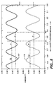
- Calculated emissivity data are shown in curves of Figure 8. These curves are the same when the layer is being increased in thickness as when it is being decreased.
- One interference curve 117 results from processing the signals from the ⁇ 1 receiving photodetectors 97 and 109, and a second interference curve 119 is obtained from the signals from the ⁇ 2 receiving photodetectors 99 and 111.
- the calculation of emissivity described above is made twice, once for each wavelength.
- Additional data can be acquired for a third or more distinct wavelengths, thus giving one or more additional interference curves, but the complexity of implementing such a system generally outweighs the advantages of doing so.
- the periods of the curves 117 and 119 are different because of the different wavelengths at which the data is acquired. Their peaks and valleys are thus not aligned. This allows the thickness of the transparent layer of the surface 13 to be determined from the data forming both of the curves 117 and 119.
- the two values of the curves are unique for each value of layer thickness, at least over a significant range of thicknesses.
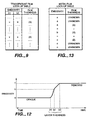
- the table of Figure 9 illustrates this.
- Each of the pairs of emissivity values for the two wavelengths corresponds to a specific thickness of the layer being monitored.
- the thickness of the layer is (A).
- A the thickness of the layer is (B).
- B a combination of values from the curves 117 and 119 of v and x gives a thickness (B).
- the table of Figure 9 is empirically determined for a specific layer material. An instrument that is capable of measuring the thickness of two or more types of materials has a separate look-up table for each material.
- ambient radiation can exist in the processing machine or environment in which the measurements are taken. This can, of course, affect the accuracy of the surface measurements.
- the measuring instrument can be shielded from such optical radiation in many cases, its effect can alternatively be effectively eliminated by modulating the incident radiation at a frequency other than that at which the ambient radiation may be modulated. That is, the power supply frequency and harmonics (60, 120 Hz. etc. in the U.S.) are avoided. Frequencies of any electrical noise generated in the processing machinery, which can be induced into the measurement circuits carrying low level signals, are also avoided.
- the photodetector output is then applied to an electronic bandpass filter to pass a narrow band of frequencies around the modulating frequency.
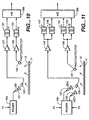
- Such a technique is shown in Figure 10, wherein the power supply 43a to an LED 121 is modulated with a sinusoidal signal having a frequency f1, such as several hundred Hz., depending on the situation.
- Background and reflected radiation photodetectors 121 and 123 apply their electrical signal to respective amplifiers 127 and 129.
- the amplified signals are then passed through respective filters 131 and 133 having narrow pass bands around the frequency f1.
- the electrical outputs of the filters 131 and 133 therefore represent the optical signals resulting from illumination by the LED 121 without optical or electrical noise introduced by the environment.
- Some characteristic of the filtered alternating current signals such as their root-mean-square (rms), is taken as representative of the surface characteristic being measured, before further arithmetic processing.
- This LED modulation technique can also be adapted to serve an additional function in a multiple wavelength instrument, as a variation of the embodiment of Figure 7.
- Figure 11 shows LEDs 135 and 137, emitting optical radiation at respective distinct wavelengths ⁇ 1 and ⁇ 2, being modulated at respective distinct frequencies f1 and f2.
- electrical bandpass filters are used. Only one reference radiation photodetector 139 is used, and only one photodetector 141 receives LED radiation reflected from the surface 13. Photodetector outputs are amplified by pre-amplifiers 143 and 145.
- the amplified signal from the photodetector 139 is applied to two filters 147 and 149, which each pass narrow frequency bands around one of the LED modulating frequencies f1 and f2, respectively.
- the amplified signal from the photodetector 141 is applied to two filters 151 and 153, which pass the frequencies f1 and f2, respectively.
- the four filter outputs are then digitized by the analog-to-digital convener 39b.
- the controller 41 ( Figure 1) then processes the signals from the f1 bandpass filters 147 and 151 to obtain data for one of the curves of Figure 8, and also processes the signals from the f2 bandpass filters 149 and 153 to obtain data for the other curve.
- the optical detection of films of normally opaque materials such as metals has typically been limited to determining when a breakthrough occurs during removal of the film by detecting when the amplitude of reflected radiation changes from one level to another in response to the metal being totally removed.
- a measurement of the reflectivity or emissivity of a metal layer can provide a measurement of its thickness when very thin.
- the shape of the curve in Figure 12 is for a copper layer over a layer of tantalum, as an example, the combination of which is carried by another material, usually a dielectric, on a substrate. Copper is used for conductors in integrated circuits.
- the layer of tantalum, or some other appropriate material provides a barrier to prevent copper from diffusing into the underlying dielectric.
- the emissivity of the two layer structure when at their fill thicknesses, is a ( Figure 12), but when the copper layer is very thin, between thicknesses (X) and (Y), its emissivity varies in a measurable manner between a and b, as a function of its thickness.
- the thickness at (X) is about 1,000 Angstroms.
- the underlying tantalum is thin enough to not be completely opaque, its emissivity also varying in a measurable manner between levels b and c as a function of its thickness, as indicated between thicknesses (Y) and (Z) in Figure 12.
- the emissivity c is that of the material under the tantalum, usually a dielectric.
- Such thin layers of metal are becoming extensively used in semiconductor processing and structures.
- the techniques of the present invention may be used to measure thickness of thin metal layers in situ during their formation, thinning or complete removal from all or portions of a wafer.
- a dielectric layer is formed to cover the wafer except where contacts need to be made through the dielectric layer to aluminum, polysilicon, substrate diffusions and the like. Shallow trenches are formed in the dielectric to define where the copper conductors are to be placed.
- a thin (typically 200-800 Angstroms) barrier layer, such as tantalum, is then deposited over the entire dielectric, including the trenches and vias through the dielectric.
- a copper layer is then formed, usually by electroplating, over the barrier layer. CMP is then used to remove the copper and underlying barrier layer from the top surface of the dielectric, leaving them in the trenches and vias where the copper conductors are desired to remain.
- Figure 13 is a look-up table that provides empirically determined data relating the emissivity and layer thickness of the curve of Figure 12. Measurements of emissivity, made by one of the ways described previously, are then converted to thickness by use of such a look-up table.
- the dual wavelength and modulated source techniques may also be used with metal layers.
- the thickness of a thin metal layer when in a region such as between (X) and (Y) of Figure 12, can be carefully controlled both during its formation and during its removal.
- the data of that characteristic curve are monitored from right to left, and when the layers are being removed, from left to right. It is also useful to monitor the thickness of a layer when it is being totally removed since this can give the process controller or the operator an indication when that end point is about to be reached.
- a very significant application of the various aspects of the present invention is the in situ measurement of layer thickness during its removal, at least partially, by CMP.
- CMP The largest application of CMP is in semiconductor wafer processing.
- CMP machines There are many different types of CMP machines being used and contemplated for use in the future. They provide relative motion with pressure between the layer surface and a pad, with a slurry of liquid chemical etchant and abrasive particles between them. It is difficult to optically monitor processes of such machines in situ because of the complex motion usually given to the substrate and layer being measured, limited optical access and optically hostile environment.
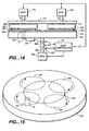
- Figures 14 and 15 show installation of a film thickness monitor according to the present invention on a CMP machine.
- Wafers 161 and 163 carry respective layers 165 and 167 that are being reduced in thickness.
- the backsides of the wafers are attached to respective wafer carriers 169 and 171.
- the wafer carriers are rotated by respective electrical motors 173 and 175.
- a structure 177 holds the wafer carriers in position.
- the wafer layers are urged against a pad 179 that is attached to a round platen 181 that itself is rotated by an electrical motor 183.
- a layer 185 of a liquid chemical etchant and abrasive particles in a slurry is applied to the pad 179. Material is removed from exposed surfaces of the wafer layers 165 and 167 by grinding them across the pad 179 with the abrasive slurry between them.
- the sensor head 15 described above preferably the version shown in Figure 6, is installed in the platen 181 in a position to look up to reflect light off of the layers being processed as they move over the head 15.
- a transparent window 187 is installed in the pad 179 over the sensor 15.
- Optical radiation generated within the head 15 then travels upward through the window 187, through the slurry 185, strikes the wafer layers in turn that are being processed, and returns back through the same path to the gathering optics within the head 15.
- the head electronics 23 is attached underneath the platen 181. Communication of its digital output signals and control signals with the host controller 25 can occur through a slip-ring assembly 189 on a rotating shaft 191 of the platen 181. Alternatively, wireless communication can be utilized, such as with the use of infra-red or radio frequency frequencies.
- the optical path between the sensor head 15 and the wafer layer being monitored is not unencumbered.
- the slurry 185 although largely transparent to the interrogating radiation, affects the optical radiation that must pass through it twice, once in each direction.
- the sensor head of the present invention overcomes this difficulty to provide good measurements.
- the wide angle radiation illumination and collection, as described above, minimizes adverse effects of the changing optical properties of the slurry over time, particularly changing radiation scattering.
- the present invention thereby makes it possible to accurately measure the thickness of the layers being processed, while they are being processed.
- Figure 15 shows the platen 181 with the position in space of the wafers 161 and 163, as well as additional wafers 162 and 164, shown in dotted outline.
- Each of the four wafers is rotated in the direction indicated with arrows by its individual driving motor.
- the direction of rotation of the platen 15 is also indicated by an arrow.
- the sensor head 15 is thus scanned in a path 193 across all four rotating wafers, one at a time.
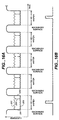
- An example emissivity signal obtained from the sensor head electronics 23 ( Figure 1) is shown in Figure 16A.
- This signal provides the emissivity (or, alternately, can be the reflectivity, if desired) of each wafer in turn as it is being scanned by the sensor 15, with the emissivity (or reflectivity) level of some other portion(s) of the CMP machine being measured as the sensor 15 moves between wafers.
- a rotational position encoder 195 attached to the rotating platen shaft 191 is read by a sensor 197, from which the host controller 25 generates relative position pulses such as those shown in Figure 16B.
- the encoder and sensor 195 and 197 can be of any suitable mechanical, optical, magnetic or other known type.
- the position pulses have a purpose of allowing the host controller to correlate the received data with an individual wafer.
- the host controller 25 can easily separate the stream of data obtained from the sensor head electronics 23, as shown in Figure 16, into separate that from the wafers and that from the portions of the processing machine in between the wafers. This is because of a sharp change in emissivity level that will normally occur as the sensor head 15 passes across an edge of a wafer. For example, such a change occurs at a signal edge 201 as the sensor head 15 passes across an edge of the wafer 161 and onto the wafer. As the sensor head 15 leaves the wafer 161, passing from it to view some other surface, an edge 203 in the signal of Figure 16A occurs. As the processing of the wafer 161 proceeds, the measured level of its emissivity changes, for example, between two levels 205 and 207.
- a signal 209 is indicated for a given wafer location a defined distance from a wafer edge. This wafer location can be selected, for example, to be where integrated circuits are formed, or, alternatively, nearer wafer edges where integrated circuits are not formed.
- the signal 209 varies over time, in a manner of the examples of Figures 8 and 12. Each time the sensor head 15 passes over the location of the waver 161 where the signal 209 is taken, a new emissivity data point is acquired for that location. Monitored data may be selected by the host controller 25 for each of the other three wafers that have the same position with respect to their edges as the data 209 of the wafer 161. By using such a common location, the layer thickness may be compared among wafers.
- Non-uniform processing shows as a variation of the data 205 in a single span, for example, between the edges 201 and 203.
- Statistical calculations can be made by the host processor 25 of data from a particular wafer to provide an indication of a spread of the emissivity values across that wafer, either from a single scan or from multiple scans across it. Further, polishing rates may be calculated from the emissivity data, either at one or more specific wafer locations with respect to an edge or on the average across a portion or the entire wafer.
Abstract
Description
- This invention relates generally to techniques for determining conditions of surfaces, and, more specifically, to doing so by measuring a characteristic of the reflectivity and/or emissivity of surfaces. An example application is the measurement of the thickness of a film on a substrate, such as a film that is formed or removed from a semiconductor wafer during the fabrication of integrated circuits. The thickness measurement is made either simultaneously with the film processing (in situ) or thereafter (in line). More specific applications include in situ measurements of the thickness of a film being reduced or removed by techniques such as wet etching, plasma etching, spin etching or chemical-mechanical-polishing (CMP).
- As a result of the development of new semiconductor processing techniques and a steadily shrinking minimum semiconductor element size, a need exists to constantly improve techniques of monitoring and measuring the results of processing, and also to develop new ones. The trend is to make as many measurements of semiconductor wafers as possible in situ, which is usually more difficult to do than as a separate step after the processing. An example of one recent development is described in U.S. patent no. 5,769,540, wherein the reflectivity of a surface is measured, from which its emissivity and/or temperature can be determined without contacting the surface. The emissivity measurement is also usable to determine the thickness of a film carried by the substrate. These techniques are particularly useful for making in situ measurements during rapid thermal processing (RTP). Another development, described in U.S. patent no. 5,695,660, measures the thickness or level of planarization of both dielectric and metal layers in situ by optical or thermal techniques during etching or CMP, including making the measurements through the back side of the wafer. When applied to CMP, an optical signal communicates with a wafer being processed through an optical window provided in one of the moving elements such as the wafer carrier. In published international (PCT) application no.
WO 97/25660, multiple sensors are carried by a moving component of a CMP machine, with a wireless communication of measurements and control signals provided between the sensors and a host control station. Other patent documents of interest include U.S. patents nos. 5,138,149, 5,190,614, 5,166,525, 5,292,605, 5,308,447, 5,362,969, 5,717,608 and 5,786,886, and PCT publication no. WO93/25893. Each of the foregoing patent publications is from Luxtron Corporation of Santa Clara, California, the assignee hereof, and is incorporated herein in its entirety by this reference. - It is a principal object of the present invention to provide further improvements to methods and instruments for optically measuring characteristics of surfaces, such as surfaces of circuit structures partially formed on semiconductor wafers or flat panel displays.
- It is a more specific object of the present invention to provide such further improvements to monitor the effects CMP processing.
- It is another object of the present invention to provide improved optical methods and instruments for measuring the thickness of layers of dielectric, semiconductor or metal materials carried by a substrate.
- It is a further object of the present invention to carry out the foregoing objects simultaneously with processing the surface or layer being monitored (in situ).
- It is an even more specific object of the present invention to accurately measure the changing thickness of a layer carried by a substrate, such as a semiconductor wafer, while being processed (in situ) to increase or decrease the layer thickness.
- These and additional objects of the present invention are realized by the various aspects of the present invention, which are briefly and generally summarized.
- A surface being monitored is illuminated by optical radiation with rays of the incident radiation spread over a wide angle to form a radiation field modified by the surface that is also collected over a wide angle and detected by a sensor. The angles of optical radiation illumination and collection are made sufficiently wide so that variations in an optical radiation path and/or of the surface being monitored, other than of the surface optical characteristic of interest, that occur over time or between different copies of the surface are minimized or substantially eliminated in order to improve the accuracy of the resultant measurements. In typical applications, the incident radiation is preferably spread over an angle of at least 45 degrees and up to 180 degrees when striking the surface being monitored, and is also preferably collected over an angle of 45 degrees or more, and up to 180 degrees. As the illumination angle is increased, the collection angle can be made narrower. The collected radiation is detected, and the detected radiation is processed to monitor a desired characteristic of the surface. Specific structures of sensors include use of an optical radiation spreading element, such as a diffuser or multi-pass reflector, positioned near to the surface being monitored, and an optical collection element, such as an end of an optical fiber or a lens, is positioned to receive the spread radiation after being modified by the surface, such as by reflection from the surface. Random or pseudo-random scattering of the illumination radiation is preferred, such as occurs when the optical radiation incident on the surface being monitored has passed through ground glass.
- The wide angle illumination and detection significantly reduces the effects of variations in scattering of the optical signals that can occur independently of the quantity desired to be measured. The incident optical radiation, and that modified by the surface being monitored, can be scattered varying amounts that depend upon the surface, angles that the radiation strikes the surface and optical elements, changes over time, and other causes. If narrow angles are viewed, for example, any variation in the amount of incident radiation that is scatted into the narrow viewing angle because of differences in scattering properties across the surface being monitored or between different surfaces, versus that which is scattered over wider angles out of view, causes the detected optical signal to vary. Significant variations can also occur when the surface is being viewed through a liquid layer, such as an etchant or slurry, that changes its thickness and other characteristics over time. These factors often cause the measurement signal to have significant amounts of undesired noise. But if the surface is viewed over most or all the angles through which the incident radiation can be scattered by the surface, any liquid etchant on it and by the optical elements, this source of noise is significantly reduced. It is reduced further when the surface is illuminated over wide angles. Illumination and detection over a full hemisphere is ideal but significant improvements are made when lesser angles in the range given above are utilized.
- The term "optical radiation" is used in this application to mean electromagnetic radiation in a continuous wavelength range including visible and near visible infrared and ultraviolet wavelengths, generally considered to extend from about 0.2 to about 4 microns. Monitoring the optical radiation modified by a surface usually also includes monitoring the level of radiation incident upon the surface so that the reflectivity or emissivity of the surface, or a related quantity, can be calculated either as the ultimate surface characteristic to be determined or as an intermediate quantity used to calculate some other surface characteristic. By making the measurements in a defined radiation wavelength range and with the geometric constraints discussed above, resulting calculations of the reflectivity or emissivity of the surface are highly meaningful because they are independent of changing conditions unrelated to surface reflectivity and emissivity. The calculation of emissivity is preferred because it is understood in the scientific community to be independent of the geometry, wavelength and other factors that can cause undesired variations in optical measurements.
- When a layer of material being formed on or removed from a substrate, in whole or in part, is being monitored, it is preferably illuminated and viewed in the above described manner. An endpoint to the complete removal of a layer is one characteristic of the surface that may be determined. Another characteristic is the thickness of the layer, either in relative or absolute terms. Because surface reflectivity or emissivity is being determined with the effects of varying measurement conditions being minimized, the thickness of a layer can be determined with a high degree of accuracy by a look-up table, model or other relationship between the reflectivity or emissivity and thickness.
- When the monitored layer is a metal or other generally opaque material, its reflectivity and emissivity are directly related to the thickness of the layer if the layer is thin enough to be at least partially transparent. For example, when a metal layer is being removed from a substrate, the layer's reflectivity or emissivity, when measured by the techniques summarized above, is directly related to the thickness of the metal layer once it has become thin enough to be semi-transparent. A metal film on a semiconductor wafer is semi-transparent when its thickness is less than about 500 to 1500 Angstroms, depending on the metal and the wavelength of radiation used. Therefore, for such thin metal layers, their thicknesses can be determined from a look-up table or set of functions that relate the measured reflectivity or emissivity with the layer's thickness. This makes it possible to measure and control the thicknesses of thin metal films with precision. Once the metal film is completely removed, then the optical properties being measured are those of the layers under the metal film. The measurement of the reflectivity or emissivity of a metal layer can be conducted with one or more wavelengths of optical radiation.
- The thickness of a layer of transparent material, such as a dielectric, can be monitored throughout a range of its entire thickness by viewing a signal resulting from interference of a portion of the incident optical radiation reflected from an outside surface from which material is being removed and another portion of the incident radiation reflected from some other interface in the structure of the substrate and layer. A given table or set of functions are used to relate specific values of the interference signal with layer thicknesses. Interference signals are preferably generated in at least two different wavelengths of optical radiation. Precise measurements of the thickness of a transparent layer are then obtainable without ambiguity under many circumstances when the two or more optical radiation wavelengths and ranges of layer thicknesses are suitable. In other cases, such precision additionally requires knowledge of the approximate layer thickness, as determined by observation or otherwise, in order to obtain a precise measurement of the transparent layer's thickness without ambiguity.
- When two or more wavelengths of radiation are used to illuminate a layer, the radiation can be generated by separate narrow bandwidth radiation sources, such as light emitting diodes (LEDs), and then the uniquely responsive to one of the source wavelengths. Alternatively, or in combination, the two or more radiation sources are each modulated with a unique frequency. Electrical signals obtained from a single or multiple radiation receiving photodetectors are then filtered to pass the source modulating frequencies in order to obtain a separate signal for each of the illumination wavelengths. The frequencies of modulation are preferably selected to be different from that of any ambient radiation or electrical noise that might be present in the environment in which the measurements are being taken, thereby to significantly reduce adverse effects of any such ambient radiation and noise. The radiation source modulation and photodetector signal filtering technique can also be used when a single optical radiation is directed at the surface being monitored in order to similarly reduce the effects of any ambient radiation and electrical noise that might be present at different frequencies from the modulating frequency.
- Although the techniques summarized above are useful to measure a surface characteristic in-line or off-line when processing of the surface is not taking place, it is usually preferable to apply these techniques to in situ monitoring. This saves the extra steps necessary to make the measurements and provides the results in real time. The processing can then be controlled from the measurements, either automatically or by providing the measurements to an operator who then adjusts the processing. One specific processing method where these measurement techniques are particularly useful is CMP, where one or more substrates (such as semiconductor wafers) are held by a carrier, and their exposed surfaces moved across a polishing pad carried by a platen. A slurry of abrasive particles and a chemical etchant is usually also used on the pad. One or more optical radiation sensors, preferably of the wide radiation angle type described above, are installed in either the carrier, if the processing is being viewed from the back side of the substrates, or in the platen, if being viewed from the front side of the substrates. The front side of the wafers can also be periodically viewed in some CMP machines when the wafers are being loaded into or unloaded from the CMP machine, or are periodically moved off the platen within the CMP machine during the CMP process.
- An analog signal obtained from a sensor installed in a CMP machine platen is a continuous one, resulting from being scanned across the one or more wafers held by the carrier and the surface of the carrier in between the wafers. If the reflectivity and emissivity of the carrier surface is significantly different than that of the wafers, there is a significant discontinuity of the signal obtained by the photodetector as its view crosses an edge of the wafer. Discrete measurements of the wafer surface are referenced to these discontinuities as a way of identifying the positions of the measurements. In some cases it is desired to take specific measurements near an edge of the wafer outside of patterned circuit die, and in others it is desired to take specific measurements over a patterned location. Control of the location is made possible by use of the edge discontinuity. The measurements at specific positions of the wafers are then monitored over time in order to measure the effect of the processing on the wafer surface.
- The representative features of the present invention described above can be implemented alone without use of the others but various combinations of the foregoing summarized features and others are alternatively combinable for use in specific applications. Additional features, advantages and objects of the various aspects of the present invention are included in the following description of various embodiments, which description should be taken in conjunction with the accompanying drawings.
-
- Figure 1 schematically illustrates in general terms a system for optically scanning a substrate to monitor a characteristic of the substrate surface;
- Figures 2 and 3 show, in cross-section, alternative versions of a general optical scanning head of Figure 1;
- Figure 4 shows the primary components of a first specific embodiment of the optical scanning head of Figure 1;
- Figure 5 is a cross-sectional view of the optical head of Figure 4;
- Figure 6 shows the primary components, in cross-section, of a second specific embodiment of the optical scanning head of Figure 1;
- Figure 7 shows a modified optical arrangement for the system of Figure 1 to make measurements at two wavelengths;
- Figure 8 are exemplary curves of measurements made of a transparent film with two wavelengths according to the system of Figure 1, as modified by the optics of Figure 7;
- Figure 9 is a table that illustrates use of the curves of Figure 8;
- Figure 10 shows another modified optical arrangement for the system of Figure 1 that modulates the illuminating optical radiation source;
- Figure 11 shows another modified optical arrangement for the system of Figure 1 that modulates illuminating optical radiation sources and makes measurements at two wavelengths;
- Figure 12 is a curve of a measurement made of a metal film according to the system of Figure 1;
- Figure 13 is a table that illustrates use of the curve of Figure 12;
- Figure 14 is a side view of one type of CMP machine;
- Figure 15 schematically illustrates relative motion of various components of the CMP machine of Figure 14; and
- Figures 16A and 16B are exemplary signals occurring in the CMP machine of Figures 14 and 15.
-
- Referring initially to Figure 1, a system utilizing the measurement techniques of the present invention is illustrated in general terms. A substrate or
other object 11 contains asurface 13 that is being measured. Anoptical sensor head 15 directs optical radiation from one or more light emitting diodes (LEDs) against aspot 17 of thesurface 13. Other sources of optical radiation can be used instead of LEDs but it is preferred that they have a narrow bandwidth, such as a few dozen nanometers in wavelength, or less. Highly coherent sources of optical radiation are unnecessary. A portion of the source radiation that is reflected from the surface is gathered by suitable optics, such as anoptical fiber 19. Other optics, such as anoptical fiber 21, collects a portion of the source radiation, preferably without any significant amount of radiation reflected from the surface, as background radiation that is used as a reference. - The
sensor head 15 is connected with amodule 23 that includes optical and electronic elements to interface between thesensor 15 and ahost controller 25, such as a personal computer. Photodetectors 27 and 29 receive the optical signals from theoptical fibers respective lines respective amplifiers digital converter 39. The amplified and digitized outputs of thephotodetectors controller 41 which controls operation of thesensor 15 and of themodule 23, and can make a portion or all of the calculations necessary to determine the ultimate quantity related to the characteristic of thesurface 13 that is being measured. Themodule 23 also includes apower circuit 43 that supplies, through aline 45, the LEDs or other optical radiation source included within thesensor head 15. The power is supplied by thehost controller 25 but controlled by thecontroller 41, themodule 23 is preferably provided in a small rugged package so that it may be positioned near thehead 15 in a piece of processing machinery. - The size of the illuminated
spot 17 is made to suit the measurement, a range of one-quarter to three-fourths of an inch in diameter for the applications specifically described herein. A diameter of thesensor head 15 of about one-half of one inch is preferred for the CMP applications described below, resulting in aspot 17 having a diameter something less than that, depending upon the optical elements at the end of thehead 15. The size of thespot 17, of course, determines the area of thesurface 13 that is averaged or integrated during each measurement. - Measurements can be made at a single point of the
surface 13, at multiple points, or continuously across thesurface 13, such as along apath 47, by providing relative motion between thehead 15 andsurface 13. Either thehead 15 can be moved, or thesubstrate 11 moved, or both. In the CMP application described below, both are moved. - Figure 2 shows a conceptual cross-sectional view of an end portion of the
sensor head 15. Optical radiation from the source(s) (not shown in Figures 2 and 3) contained in thehead 15 is directed through an optical radiation spreading element that extends across an end opening of acylindrical housing 51. Theelement 49 spreads the source radiation over a maximum angle , preferably with substantially uniform intensity. A diffraction element may be made for this purpose but use of ground glass for theelement 49 operates satisfactorily and provides a randomness to the surface illumination. As discussed above, better results are obtained as the angle increases. Theelement 49 is designed to provide this angle to be at least 45 degrees. - An end of an optical fiber has an acceptance angle of optical radiation that depends primarily upon the refractive index of the fiber core material. Such an angle Φ is shown on Figure 2 at an end of the
optical fiber 19, which extends through theelement 49 to have an unobstructed view of thesurface 13. It is also desirable that this angle be made as large as is practical, as discussed above, preferably 45 degrees or more. An optical fiber with a core made of sapphire, quartz or cubic zirconia has an angle of acceptance of about 45 degrees. For a larger angle Φ, or when other optical fiber cores with a lower refractive index are used, such as plastic, alens element 53 can be added to the end of theoptical fiber 19, as shown in Figure 3. The diameter of the area viewed by theoptical fiber 19 is increased, as indicated in Figure 3. It is the area of thesurface 13 within the angle of acceptance Φ that defines thespot 17, assuming that this area is also substantially uniformly illuminated. - One specific embodiment of a
sensor head 15 is shown in Figures 4 and 5, where elements that are counterparts of those described above are identified by the same reference numbers but, when different in structure, have a prime (') added to the reference number. A plurality of LEDs 55-64 are distributed around ahemispherical shell 65. Atransparent cover 67 may be provided with radiation scattering properties but a wide distribution of radiation results from the numerous LEDs and internal reflection within theshell 65. Thesurface 13 is illuminated with a range of angles close to 180 degrees, depending upon the distance between the shell and thesurface 13. Lenses provided as part of the LEDs may also be roughened to add to the diffusion of the illumination provided by thehead 15 of Figures 4 and 5. - Another specific embodiment of a
sensor head 15, which is preferred, is shown in cross section in Figure 6. Within thecylindrical shell 51 are a plurality of LEDs, includingLEDs diffuser 77 through which the radiation gatheringoptical fiber 19 extends, similar to the structure of Figures 2 and 3. When used in hostile environments, such as in semiconductor liquid etch or CMP machines, the sensor head 15'' is sealed against liquids, moisture and gas vapors. This can be done at one end by sealing thediffuser 77 to thediffuser 77 but a better seal is obtained by adding a single piececlear glass plate 79 which extends completely across and is sealed to the inside of theshell 51. Optical radiation from the LEDs is gathered into theoptical fiber 17 by positioning a circulardiffusive reflecting element 81 around theoptical fiber 19. Theelement 81 is made small enough so as not to block thediffuser 77 from receiving almost all of the radiation from the LEDs but large enough to reflect enough of the radiation into theoptical fiber 17 to obtain a useful background reference signal. - The wavelength of the optical radiation source is chosen to be the best for monitoring the particular surface characteristics of interest. The radiation needs to interact with the feature or characteristic of the object or its surface that is desired to be monitored, in a way that can be detected in the radiation after being modified by the object. For silicon semiconductor monitoring by reflecting radiation from a wafer, wavelengths slightly below the band edge of silicon are usually best, generally infra-red radiation less than one micron, to which the wafer is opaque. If radiation is transmitted through the object being monitored to obtain an object modified beam that is detected, the radiation is, of course, chosen to be of a wavelength that will pass through the object.
- When the reflectivity of the
surface 13 is being measured, thecontroller 41 calculates a ratio of the reflected radiation signal from thephotodetector 27 to the background radiation signal from thephotodetector 29, as is well known. The instrument is first calibrated by positioning thesensor head 15 against at least one surface having a known reflectivity, and preferably against several surfaces having known different reflectivities. Calibration includes adjusting the relative gains of the two signal channels until the instrument reads the known reflectivity of the test surface. This is preferably done by software within thecontroller 41, particularly when multiple test surfaces are used. - When the emissivity of the
surface 13 is being measured, the controller subtracts the reflectivity from unity, as is well known. The instrument is similarly calibrated by using test order t surfaces of known emissivities. In the examples to follow, emissivity of a surface is calculated as a measure of the thickness of a layer of material that forms that surface. The primary application is in semiconductor processing but the techniques are not so limited. As is well known, a changing thickness of a dielectric material, which is transparent to the incident radiation, is monitored by measuring the interference of the radiation reflected from both surfaces of the layer. The interference signal passes through peaks and valleys as the layer either becomes thicker when being formed by chemical vapor deposition (CVD) or otherwise, or becomes thinner as material is removed by wet or dry etching, CMP or some other technique. - The ability to determine an absolute thickness of a dielectric layer, rather than only a relative thickness or rate of change of the thickness, is provided by the present invention by making the measurement separately at different wavelengths and then combining the results. Figure 7 shows a modification of the single wavelength embodiments described above. Two different types of
LEDs surface 13 and gathered by anoptical fiber 93, passed to abeam splitter 95 and thence tophotodetectors optical fiber 105 which directs the radiation sampled from theLEDs beam splitter 107. A portion of the reference radiation then strikes aphotodetector 109 through anoptical filter 113 that passes λ1, and another portion reaches aphotodetector 111 through anoptical filter 115 that passes λ2. The electrical outputs of these photodetectors are also applied to the analog-to-digital converter 39'. - The controller 41 (Figure 1) now calculates the reflectivity or emissivity of the
surface 13 separately for each of the radiation wavelengths λ1 and λ2. Calculated emissivity data are shown in curves of Figure 8. These curves are the same when the layer is being increased in thickness as when it is being decreased. Oneinterference curve 117 results from processing the signals from theλ1 receiving photodetectors second interference curve 119 is obtained from the signals from theλ2 receiving photodetectors curves surface 13 to be determined from the data forming both of thecurves - The table of Figure 9 illustrates this. Each of the pairs of emissivity values for the two wavelengths corresponds to a specific thickness of the layer being monitored. For example, when the emissivity is calculated to be u and w for the respective wavelengths λ1 and λ2, it is known that the thickness of the layer is (A). This is also shown on the curves of Figure 8. Similarly, a combination of values from the
curves photodetectors - Depending upon the particular range of layer thicknesses and specific wavelengths used, long sequences of pairs of emissivity readings can repeat themselves in the look-up table of Figure 9, and thereby introduce an ambiguity in the thickness readings made. When this occurs, an additional piece of information is given the controller 41 (Figure 1), such as the approximate thickness at the beginning of an etch or CMP process. The user can input this information when the process is begun. This then allows the controller to start with the proper thickness value in response to a pair of emissivity readings that occurs more than once in the table. Use of a third or more emissivity readings can eliminate the ambiguity in many cases. When the measurement is being made of the thickness of a layer being formed, it is known to start making readings in the look-up table at zero thickness, so any repeating sequences of values do not cause an ambiguous thickness calculation.
- Depending on the wavelength(s) at which the measurements are made, ambient radiation can exist in the processing machine or environment in which the measurements are taken. This can, of course, affect the accuracy of the surface measurements. Although the measuring instrument can be shielded from such optical radiation in many cases, its effect can alternatively be effectively eliminated by modulating the incident radiation at a frequency other than that at which the ambient radiation may be modulated. That is, the power supply frequency and harmonics (60, 120 Hz. etc. in the U.S.) are avoided. Frequencies of any electrical noise generated in the processing machinery, which can be induced into the measurement circuits carrying low level signals, are also avoided. The photodetector output is then applied to an electronic bandpass filter to pass a narrow band of frequencies around the modulating frequency. Such a technique is shown in Figure 10, wherein the
power supply 43a to anLED 121 is modulated with a sinusoidal signal having a frequency f1, such as several hundred Hz., depending on the situation. Background and reflectedradiation photodetectors respective amplifiers respective filters filters LED 121 without optical or electrical noise introduced by the environment. Some characteristic of the filtered alternating current signals, such as their root-mean-square (rms), is taken as representative of the surface characteristic being measured, before further arithmetic processing. - This LED modulation technique can also be adapted to serve an additional function in a multiple wavelength instrument, as a variation of the embodiment of Figure 7. Figure 11 shows
LEDs reference radiation photodetector 139 is used, and only onephotodetector 141 receives LED radiation reflected from thesurface 13. Photodetector outputs are amplified bypre-amplifiers photodetector 139 is applied to twofilters photodetector 141 is applied to twofilters digital convener 39b. The controller 41 (Figure 1) then processes the signals from the f1 bandpass filters 147 and 151 to obtain data for one of the curves of Figure 8, and also processes the signals from the f2 bandpass filters 149 and 153 to obtain data for the other curve. Thus, if the modulating frequencies f1 and f2 are both chosen to suppress optical and electrical environmental noise in the manner discussed above with respect to Figure 10, the system of Figure 11 has that advantage as well. Additionally, the systems of Figures 7 and 11 can be combined by using both optical and electrical filters. - The optical detection of films of normally opaque materials such as metals has typically been limited to determining when a breakthrough occurs during removal of the film by detecting when the amplitude of reflected radiation changes from one level to another in response to the metal being totally removed. However, as illustrated by the curve of Figure 12, a measurement of the reflectivity or emissivity of a metal layer can provide a measurement of its thickness when very thin. The shape of the curve in Figure 12 is for a copper layer over a layer of tantalum, as an example, the combination of which is carried by another material, usually a dielectric, on a substrate. Copper is used for conductors in integrated circuits. The layer of tantalum, or some other appropriate material, provides a barrier to prevent copper from diffusing into the underlying dielectric. The emissivity of the two layer structure, when at their fill thicknesses, is a (Figure 12), but when the copper layer is very thin, between thicknesses (X) and (Y), its emissivity varies in a measurable manner between a and b, as a function of its thickness. For copper, the thickness at (X) is about 1,000 Angstroms. In this example, the underlying tantalum is thin enough to not be completely opaque, its emissivity also varying in a measurable manner between levels b and c as a function of its thickness, as indicated between thicknesses (Y) and (Z) in Figure 12. The emissivity c is that of the material under the tantalum, usually a dielectric.
- Such thin layers of metal are becoming extensively used in semiconductor processing and structures. The techniques of the present invention may be used to measure thickness of thin metal layers in situ during their formation, thinning or complete removal from all or portions of a wafer. When copper is used for conductors, a dielectric layer is formed to cover the wafer except where contacts need to be made through the dielectric layer to aluminum, polysilicon, substrate diffusions and the like. Shallow trenches are formed in the dielectric to define where the copper conductors are to be placed. A thin (typically 200-800 Angstroms) barrier layer, such as tantalum, is then deposited over the entire dielectric, including the trenches and vias through the dielectric. A copper layer is then formed, usually by electroplating, over the barrier layer. CMP is then used to remove the copper and underlying barrier layer from the top surface of the dielectric, leaving them in the trenches and vias where the copper conductors are desired to remain.
- Figure 13 is a look-up table that provides empirically determined data relating the emissivity and layer thickness of the curve of Figure 12. Measurements of emissivity, made by one of the ways described previously, are then converted to thickness by use of such a look-up table. The dual wavelength and modulated source techniques may also be used with metal layers.
- It can be then seen that the thickness of a thin metal layer, when in a region such as between (X) and (Y) of Figure 12, can be carefully controlled both during its formation and during its removal. When forming the two tantalum and copper layers of that example, the data of that characteristic curve are monitored from right to left, and when the layers are being removed, from left to right. It is also useful to monitor the thickness of a layer when it is being totally removed since this can give the process controller or the operator an indication when that end point is about to be reached.
- A very significant application of the various aspects of the present invention is the in situ measurement of layer thickness during its removal, at least partially, by CMP. The largest application of CMP is in semiconductor wafer processing. There are many different types of CMP machines being used and contemplated for use in the future. They provide relative motion with pressure between the layer surface and a pad, with a slurry of liquid chemical etchant and abrasive particles between them. It is difficult to optically monitor processes of such machines in situ because of the complex motion usually given to the substrate and layer being measured, limited optical access and optically hostile environment.
- Figures 14 and 15 show installation of a film thickness monitor according to the present invention on a CMP machine. In this example, four semiconductor wafers are being processed at one time.
Wafers respective layers 165 and 167 that are being reduced in thickness. The backsides of the wafers are attached torespective wafer carriers electrical motors structure 177 holds the wafer carriers in position. The wafer layers are urged against apad 179 that is attached to around platen 181 that itself is rotated by anelectrical motor 183. Alayer 185 of a liquid chemical etchant and abrasive particles in a slurry is applied to thepad 179. Material is removed from exposed surfaces of the wafer layers 165 and 167 by grinding them across thepad 179 with the abrasive slurry between them. - The
sensor head 15 described above, preferably the version shown in Figure 6, is installed in theplaten 181 in a position to look up to reflect light off of the layers being processed as they move over thehead 15. Atransparent window 187 is installed in thepad 179 over thesensor 15. Optical radiation generated within thehead 15 then travels upward through thewindow 187, through theslurry 185, strikes the wafer layers in turn that are being processed, and returns back through the same path to the gathering optics within thehead 15. Thehead electronics 23 is attached underneath theplaten 181. Communication of its digital output signals and control signals with thehost controller 25 can occur through a slip-ring assembly 189 on arotating shaft 191 of theplaten 181. Alternatively, wireless communication can be utilized, such as with the use of infra-red or radio frequency frequencies. - It can be seen that the optical path between the
sensor head 15 and the wafer layer being monitored is not unencumbered. Particularly theslurry 185, although largely transparent to the interrogating radiation, affects the optical radiation that must pass through it twice, once in each direction. But the sensor head of the present invention overcomes this difficulty to provide good measurements. The wide angle radiation illumination and collection, as described above, minimizes adverse effects of the changing optical properties of the slurry over time, particularly changing radiation scattering. The present invention thereby makes it possible to accurately measure the thickness of the layers being processed, while they are being processed. - Figure 15 shows the
platen 181 with the position in space of thewafers additional wafers platen 15 is also indicated by an arrow. Thesensor head 15 is thus scanned in apath 193 across all four rotating wafers, one at a time. An example emissivity signal obtained from the sensor head electronics 23 (Figure 1) is shown in Figure 16A. This signal provides the emissivity (or, alternately, can be the reflectivity, if desired) of each wafer in turn as it is being scanned by thesensor 15, with the emissivity (or reflectivity) level of some other portion(s) of the CMP machine being measured as thesensor 15 moves between wafers. Arotational position encoder 195 attached to therotating platen shaft 191 is read by asensor 197, from which thehost controller 25 generates relative position pulses such as those shown in Figure 16B. The encoder andsensor - The
host controller 25 can easily separate the stream of data obtained from thesensor head electronics 23, as shown in Figure 16, into separate that from the wafers and that from the portions of the processing machine in between the wafers. This is because of a sharp change in emissivity level that will normally occur as thesensor head 15 passes across an edge of a wafer. For example, such a change occurs at asignal edge 201 as thesensor head 15 passes across an edge of thewafer 161 and onto the wafer. As thesensor head 15 leaves thewafer 161, passing from it to view some other surface, anedge 203 in the signal of Figure 16A occurs. As the processing of thewafer 161 proceeds, the measured level of its emissivity changes, for example, between twolevels host controller 25 to select a location on the wafer a certain distance from an edge for measuring emissivity as the processing proceeds. Asignal 209 is indicated for a given wafer location a defined distance from a wafer edge. This wafer location can be selected, for example, to be where integrated circuits are formed, or, alternatively, nearer wafer edges where integrated circuits are not formed. Thesignal 209 varies over time, in a manner of the examples of Figures 8 and 12. Each time thesensor head 15 passes over the location of thewaver 161 where thesignal 209 is taken, a new emissivity data point is acquired for that location. Monitored data may be selected by thehost controller 25 for each of the other three wafers that have the same position with respect to their edges as thedata 209 of thewafer 161. By using such a common location, the layer thickness may be compared among wafers. - Of course, data for more than one location on each wafer may be monitored during the processing. Averages of several data points across each wafer may also be independently monitored. Or an average of all readings across a specific segment or the entire wafer can be made and turned into time based signals of the type shown in Figures 8 and 12. Further, as can be seen from the signal of Figure 16A, uniformity of the processing across a defined portion or all of the individual wafers can be monitored. Non-uniform processing shows as a variation of the
data 205 in a single span, for example, between theedges host processor 25 of data from a particular wafer to provide an indication of a spread of the emissivity values across that wafer, either from a single scan or from multiple scans across it. Further, polishing rates may be calculated from the emissivity data, either at one or more specific wafer locations with respect to an edge or on the average across a portion or the entire wafer. - It will be recognized from Figure 15 that the path 47 (Figure 1) scanned across a wafer is not the same each time because of the complex relative motion given to the wafers and the
sensor head 15 That motion, however, depends upon the particular CMP equipment with which the measuring techniques of the present invention are utilized. - Although the various aspects of the present invention have been described with respect to their preferred embodiments, it shall be understood that the invention is entitled to protection within the fill scope of the appended claims.
Claims (47)
- A method of determining a particular characteristic of a surface area, comprising:positioning at a first distance from the surface area an optical element that spreads incident optical radiation over an angle of 45 degrees or more,directing optical radiation from one or more optical radiation sources to the radiation spreading optical element and thence onto the surface area to reflect the spread radiation from the surface area,capturing, through the radiation spreading element, optical radiation reflected by the surface area with first radiation gathering optics having an angle of acceptance of 45 degrees or more and positioned a second distance from said surface area,capturing optical radiation from the one or more radiation sources with second radiation gathering optics positioned to receive optical radiation from the one or more radiation sources,detecting the optical radiation captured by the first and second radiation gathering optics, anddetermining the particular characteristic of the surface area from levels of the detected optical radiation from each of the first and second radiation gathering optics.
- The method of claim 1, wherein capturing optical radiation from the one or more radiation sources includes reflecting a portion of the optical radiation from said one or more radiation sources into the end of the second light pipe from a reflective optical radiation diffuser that is positioned in a path of optical radiation from said one or more optical radiation sources.
- The method of claim 1, wherein the particular characteristic of the surface area includes its reflectivity, and determining the reflectivity includes taking a ratio of a detected level of optical radiation captured by the first and second light pipes.
- The method of claim 1, wherein the particular characteristic of the surface area includes its emissivity, and determining the emissivity includes taking a ratio of a detected level of optical radiation captured by the first and second light pipes.
- The method of claim 1, wherein the surface area extends across a film carried by a substrate, and the particular characteristic of the film being determined includes its thickness, and determining the film thickness includes comparing a detected level of optical radiation captured by the first and second light pipes.
- The method of claim 1, wherein the surface area extends across a structure formed on a semiconductor wafer.
- The method of claim 1, wherein the surface area extends across a structure formed on a flat panel display.
- The method of any one of claims 3-7, wherein the particular characteristic of the surface area is being determined simultaneously with the surface area being processed in a manner that changes its said particular characteristic.
- The method of claim 8, wherein the surface area is being processed by chemical-mechanical-polishing.
- The method of any one of claims 1-7, wherein positioning the radiation spreading optical element includes positioning a transparent radiation diffuser the first distance from the surface area.
- The method of claim 7, which additionally comprises holding said surface area against a moving element surface, and wherein directing radiation onto the surface area includes directing radiation from the one or more radiation sources and through the diffuser that are located within the moving element.
- The method of any one of claims 1-7, wherein positioning the radiation spreading optical element includes positioning a hemispherical element having a plurality of optical radiation sources held around an inside surface thereof, which inside surface is reflective and positioned to open onto the surface area.
- The method of any one of claims 1-7, wherein directing optical radiation to the radiation spreading optical element from one or more optical radiation sources includes directing said radiation from at least one source of optical radiation of a first bandwidth and at least one source of optical radiation of a second bandwidth, said first and second bandwidths being distinct from each other.
- The method of claim 13, wherein the sources of optical radiation of the first bandwidth are driven at a first modulating frequency, the sources of optical radiation of the second bandwidth are driven at a second modulating frequency that is distinct from the first modulating frequency, wherein detecting the optical radiation includes directing the optical radiation captured by the first radiation gathering optics onto a photodetector, and wherein determining the surface area characteristic includes directing an electrical output signal from the photodetector through bandpass filters that respectively pass said first and second modulating frequencies.
- The method of claim 5, wherein directing optical radiation to the radiation spreading optical element includes directing said radiation from at least one source of optical radiation of a first bandwidth and at least one source of optical radiation of a second bandwidth, said first and second bandwidths being distinct from each other, wherein the film is transparent to the optical radiation of said first and second bandwidths, and additionally comprising:maintaining a relationship of values of thickness of the film as a function of pairs of values of the optical characteristic data at the first and second bandwidths, andrepetitively converting measured pairs of values of the optical characteristic at the respective first and second bandwidths to values of layer thickness by reference to said relationship.
- The method of claim 5, wherein the film is metal, and additionally comprising:maintaining a relationship of values of thickness of the film as a function of either reflectivity or emissivity in a region where the metal film becomes partially transparent to the optical radiation form said one or more optical radiation sources, andrepetitively converting measured pairs of values of the optical characteristic at the respective first and second bandwidths to values of layer thickness by reference to said relationship.
- The method of either of claim 15 or 16, wherein the layer characteristic determining steps are performed simultaneously with the film being reduced in thickness by a process of chemical-mechanical-polishing.
- The method of any one of claims 1-7, wherein directing optical radiation to the radiation spreading optical element includes modulating the optical radiation from said one or more optical radiation sources at a given frequency, wherein detecting the optical radiation includes directing the optical radiation captured by the first radiation gathering optics onto a photodetector, and wherein determining the surface area characteristic includes directing an electrical output signal from the photodetector through a bandpass filter that passes said given modulating frequency.
- The method of any one of claims 1-7, additionally comprising repetitively moving across the surface the area to which optical radiation is directed from said one or more optical radiation sources and from which optical radiation reflected therefrom is captured, noting a change in the detected optical radiation caused by a discontinuity on the surface, and referencing a region on the surface in a certain position with respect to the discontinuity for which said particular surface area characteristic is determined.
- The method of any one of claims 1-7, wherein capturing optical radiation reflected by the surface area by the first radiation gathering optics includes positioning an end of a first light pipe the second distance from the surface area.
- The method of claim 20, wherein capturing optical radiation from the one or more radiation sources includes positioning an end of a second light pipe to receive optical radiation from the one or more radiation sources.
- Apparatus for determining a reflective characteristic of an area of an article, comprising:a machine component having a surface adapted to be contacted by said article,a window forming a portion of said component surface,at least one source of optical radiation carried by the component on a side of the window opposite to the article contacting surface,an optical radiation spreading element carried by the component between the window and said at least one source of optical radiation, said element spreading light from said at least one source of optical radiation through the window over an angle of 45 degrees or more,a first light pipe carried by the component that extends through the spreading element with an end facing the window to gather optical radiation passing through said window from the article area, said first light pipe end having an angle of acceptance of 45 degrees or more,a first photodetector carried by the component to receive optical radiation in the first light pipe and generate a first electrical signal related thereto,a second light pipe carried by the component and having an end positioned between said at least one source of optical radiation and the spreading element to obtain optical radiation from said at least one source of optical radiation,a second photodetector carried by the component to receive radiation in the second light pipe and generate a second electrical signal related thereto, anda processor utilizing the first and second electrical signals for determining the reflective characteristic of the article area.
- The apparatus of claim 22, additionally comprising a second optical radiation spreading element carried by the component between the window and said at least one source of optical radiation in a position to direct optical radiation from said at least one source of optical radiation into the second light pipe end.
- The apparatus of claim 23, wherein the article contacting surface of the component is planar and has a back surface defining a thickness of the element therebetween, and wherein all of the window, at least one source of optical radiation, the spreading element, the second optical radiation spreading element, the first light pipe end, and the second light pipe end are positioned in a compartment formed in the component between its said article contacting and back surfaces.
- The apparatus of claim 24, wherein an electronic unit is attached to said machine component that includes amplifiers for each of the first and second electrical signals, an analog-to-digital converting circuit, and a processor, an output of the processor providing data of the article area reflective characteristic being determined.
- The apparatus of claim 25, wherein the machine component is moveable to process the article.
- The apparatus of any one of claims 22-25, wherein the component is part of a chemical-mechanical-polishing machine that is given motion while processing the article area.
- The apparatus of claim 27, wherein the component is a platen with a polishing pad as its said surface adapted to be contacted by said article.
- A method of monitoring the processing of the surface of at least one article by chemical-mechanical-polishing wherein the article is held by a first machine surface in a manner that a surface of the article is urged against a second machine surface and relative motion is provided therebetween, comprising:providing the first surface with a different reflective property than the surface of the article,providing at least one sensor recessed into the second surface in a position to be scanned across said at least one article surface as the first and second surfaces move with respect to each other and provide an electrical signal related to a reflective property of the article surface and of the first surface there around as a function of the position of said at least one sensor thereacross,detecting discontinuities in a level of the electrical signal that occur as the sensor passes across edges of the article,using at least one of said signal discontinuities as a time reference to identify at least one segment of the electrical signal occurring between the signal edge discontinuities that corresponds to a region of the article whose surface is desired to be monitored during the processing,accumulating data from repetitive occurrences of said signal segment as the sensor repetitively scans across the article surface, andconverting the accumulated signal segment data into a representation of the reflectivity or emissivity of the individual article surface throughout a period of the processing.
- The method of claim 29, wherein two or more articles are simultaneously processed, thereby to generate a signal having discontinuities as the sensor passes across the edges of each of said two or more articles, at least one electrical signal segment being identified for each of the two or more articles, data being accumulated from repetitive occurrences of each of the individual article wafer segments and the accumulated data being converted into representations of the reflectivity or emissivity of the individual article regions corresponding to the individual article signal segments.
- The method of either of claims 29 or 30, additionally comprising illuminating the article surface with incident optical radiation spread over an angle of at least 45 degrees, and capturing by the sensor a portion of the incident optical radiation reflected by the article surface over an angle of 45 degrees or more.
- An optical method of monitoring the thickness of a layer of transparent material carried by a substrate as it is being changed by processing, comprising:acquiring data of an optical characteristic of the layer at at least first and second distinct wavelengths of optical radiation, wherein said optical characteristic varies differently as a function of the thickness of the layer at said first and second wavelengths,maintaining a relationship of values of thickness of the layer as a function of pairs of values of the optical characteristic data at the first and second wavelengths, andrepetitively convening measured pairs of values of the optical characteristic at the respective first and second wavelengths to values of layer thickness by reference to said relationship, said converting occurring simultaneously with the processing changing the thickness of the layer.
- The method of claim 32, wherein acquiring data of an optical characteristic of the layer includes illuminating the surface with optical radiation including said first and second wavelengths, receiving a portion of the illuminating radiation reflected from the layer, and detecting the reflected radiation in a manner to provide separate signals related to levels of the reflected radiation at said first and second wavelengths.
- The method of claim 33, wherein detecting the reflected radiation includes providing first and second photodetectors in the path of the reflected radiation with respective first and second optical bandpass filters in front thereof, said first filter passing optical radiation of the first wavelength while blocking optical radiation of the second wavelength and the second filter passing optical radiation at the second wavelength while blocking optical radiation at the first wavelength.
- The method of claim 33, wherein illuminating the surface includes modulating illuminating radiation of said first and second wavelengths at respective first and second distinct frequencies, and wherein detecting the reflected radiation includes obtaining a photodetector electrical output signal thereof and filtering said electrical signal to pass components thereof that are related to values of the optical signal at said first and second frequencies.
- The method of claim 32, wherein the optical characteristic of the layer for which data is acquired includes an emissivity of the layer.
- The method of claim 32, wherein maintaining the relationship of values includes maintaining a table of pairs of values of the optical characteristic at said at least first and second wavelengths for each of a plurality of thicknesses of said layer, and converting measured pairs of values of the optical characteristic to values of layer thickness includes looking up the layer thickness in this table.
- The method of any one of claims 33-35, wherein illuminating the surface additionally includes directing the optical radiation against the surface over an angle of 45 degrees or more and receiving radiation reflected from the layer includes receiving said radiation over an angle of 45 degrees or more.
- The method of claim 38, wherein the optical characteristic of the layer for which data is acquired includes a reflectivity of the layer.
- The method of claim 38, wherein the optical characteristic of the layer for which data is acquired includes an emissivity of the layer
- The method of any one of claims 32-36, wherein the processing being performed on said layer is chemical-mechanical-polishing.
- A method of changing the thickness of a layer of metal carried by a substrate, comprising,:directing optical radiation against the layer over an angle of at least 45 degrees, thereby to reflect a portion of said radiation from said layer, and receiving the reflected radiation over an angle of at least 45 degrees,simultaneously processing the layer to alter its thickness,monitoring the reflected radiation as the layer is being altered in thickness from a constant value over time until the value changes but before the value becomes constant over time at a different level,comparing the value of the reflected radiation during its changing with known values as a function of the thickness of said layer, andterminating altering the thickness of the layer when the reflected radiation is determined to correspond to the desired thickness of the layer.
- The method according to claim 42, wherein the layer is being processed by CMP to remove material therefrom.
- The method of forming copper conductors on an integrated circuit structure, comprising:forming a dielectric material layer over the integrated circuit structure,forming trenches in a top surface of the dielectric material where copper conductors are to be formed,depositing a barrier layer of material over the dielectric top surface and into said trenches,depositing a layer of copper material over the barrier layer on the top surface and into the trenches of the dielectric material layer,removing by a CMP process the copper and barrier layers from the top surface of the dielectric but not from the trenches,concurrently with removing the layers, directing optical radiation against the layers over an angle of at least 45 degrees, thereby to reflect a portion of said radiation from said layers, and receiving the reflected radiation over an angle of at least 45 degrees,monitoring the reflected radiation as the layers are being removed,comparing the value of the reflected radiation during its changing with known values as a function of the thickness of said layers, andterminating the CMP process when the reflected radiation is determined to correspond to the desired thickness of the layer.
- A method of measuring, through an optical radiation scattering medium, the thickness of a layer carried by a surface, comprising:directing incident optical radiation through the scattering medium to the layer in a manner to obtain optical radiation reflected thereby, including spreading and scattering the optical radiation from one or more radiation sources prior to the incident radiation passing through the scattering medium,capturing the optical radiation reflected by the layer through the radiation scattering medium over an angle sufficient to counteract effects of variations in scattering of the optical radiation by the radiation scattering medium,capturing optical radiation from the one or more radiation sources without effect of the reflected optical radiation,separately detecting the optical radiation reflected by the layer and the optical radiation from the one or more radiation sources, anddetermining the thickness of the layer from levels of the detected optical radiation.
- The method of claim 45, wherein spreading and scattering the optical radiation includes directing the incident optical radiation through a diffuser prior to striking the scattering medium and the layer.
- The method of either one of claims 45 or 46, wherein directing optical radiation includes directing said optical radiation through the scattering medium to the layer over an angle of 45 degrees or more, and wherein capturing the optical radiation reflected by the layer includes receiving the optical radiation reflected by the layer through the scattering medium over an angle of 45 degrees or more.
Applications Claiming Priority (2)
| Application Number | Priority Date | Filing Date | Title |
|---|---|---|---|
| US09/317,697 US6570662B1 (en) | 1999-05-24 | 1999-05-24 | Optical techniques for measuring layer thicknesses and other surface characteristics of objects such as semiconductor wafers |
| US317697 | 1999-05-24 |
Publications (2)
| Publication Number | Publication Date |
|---|---|
| EP1055903A1 true EP1055903A1 (en) | 2000-11-29 |
| EP1055903B1 EP1055903B1 (en) | 2006-12-20 |
Family
ID=23234867
Family Applications (1)
| Application Number | Title | Priority Date | Filing Date |
|---|---|---|---|
| EP00304118A Expired - Lifetime EP1055903B1 (en) | 1999-05-24 | 2000-05-16 | Optical techniques for measuring layer thicknesses and other surface characteristics of objects such as semiconductor wafers |
Country Status (4)
| Country | Link |
|---|---|
| US (2) | US6570662B1 (en) |
| EP (1) | EP1055903B1 (en) |
| DE (1) | DE60032411T2 (en) |
| TW (1) | TW577974B (en) |
Cited By (6)
| Publication number | Priority date | Publication date | Assignee | Title |
|---|---|---|---|---|
| US6320609B1 (en) | 1998-07-10 | 2001-11-20 | Nanometrics Incorporated | System using a polar coordinate stage and continuous image rotation to compensate for stage rotation |
| WO2004002680A1 (en) * | 2002-06-26 | 2004-01-08 | Freescale Semiconductor, Inc. | Apparatus and method for endpoint detection and monitoring for chemical mechanical polishing operations |
| DE10123470B4 (en) * | 2001-05-15 | 2010-08-19 | Carl Zeiss Jena Gmbh | Method and arrangement for non-contact determination of product properties |
| WO2015165503A1 (en) * | 2014-04-29 | 2015-11-05 | Hewlett-Packard Indigo B.V. | Transparent layer thickness measurement |
| CN111469047A (en) * | 2020-04-14 | 2020-07-31 | 大连理工大学 | Test device for online detection of contact characteristics of polishing pad and use method thereof |
| WO2021012597A1 (en) * | 2018-08-29 | 2021-01-28 | 陈嘉朗 | Variable-frequency polarization polishing apparatus and method |
Families Citing this family (22)
| Publication number | Priority date | Publication date | Assignee | Title |
|---|---|---|---|---|
| US6368881B1 (en) * | 2000-02-29 | 2002-04-09 | International Business Machines Corporation | Wafer thickness control during backside grind |
| US20030045008A1 (en) * | 2001-08-31 | 2003-03-06 | Gregory Olsen | Method and apparatus for monitoring changes in the surface of a workpiece during processing |
| US6842235B2 (en) * | 2001-09-28 | 2005-01-11 | Infineon Technologies North America Corp. | Optical measurement of planarized features |
| IL145699A (en) * | 2001-09-30 | 2006-12-10 | Nova Measuring Instr Ltd | Method of thin film characterization |
| WO2003066282A2 (en) | 2002-02-04 | 2003-08-14 | Kla-Tencor Technologies Corp. | Systems and methods for characterizing a polishing process |
| US6762849B1 (en) * | 2002-06-19 | 2004-07-13 | Novellus Systems, Inc. | Method for in-situ film thickness measurement and its use for in-situ control of deposited film thickness |
| DE10319543B4 (en) * | 2003-04-30 | 2011-03-03 | Byk-Gardner Gmbh | Apparatus and method for determining surface properties |
| WO2005017489A2 (en) * | 2003-07-11 | 2005-02-24 | Svt Associates, Inc. | Film mapping system |
| US7204639B1 (en) * | 2003-09-26 | 2007-04-17 | Lam Research Corporation | Method and apparatus for thin metal film thickness measurement |
| US20060176487A1 (en) * | 2004-09-27 | 2006-08-10 | William Cummings | Process control monitors for interferometric modulators |
| CN101006491A (en) * | 2004-09-27 | 2007-07-25 | Idc公司 | Measuring and modeling power consumption in displays |
| US8152365B2 (en) * | 2005-07-05 | 2012-04-10 | Mattson Technology, Inc. | Method and system for determining optical properties of semiconductor wafers |
| KR100836501B1 (en) * | 2005-10-11 | 2008-06-09 | 동부일렉트로닉스 주식회사 | Image Sensor of Thin Film Processing Device for fabricating semiconductor devices |
| US8231251B2 (en) * | 2005-10-28 | 2012-07-31 | Philips Lumileds Lighting Company Llc | Multiple piece reflective angle transformer |
| US7543981B2 (en) * | 2006-06-29 | 2009-06-09 | Mattson Technology, Inc. | Methods for determining wafer temperature |
| JP5006883B2 (en) * | 2006-10-06 | 2012-08-22 | 株式会社荏原製作所 | Processing end point detection method and processing apparatus |
| US20100096553A1 (en) * | 2008-10-22 | 2010-04-22 | Honeywell International Inc. | Reflective optical sensor and switches and systems therefrom |
| DE102011101934B4 (en) * | 2011-05-18 | 2017-07-06 | Christian-Albrechts-Universität Zu Kiel | Large biofilm sensor |
| US8917398B2 (en) | 2011-08-28 | 2014-12-23 | G & D Innovative Analysis Ltd. | Method and apparatus for supervision of optical material production |
| US9360302B2 (en) * | 2011-12-15 | 2016-06-07 | Kla-Tencor Corporation | Film thickness monitor |
| DE102016116012A1 (en) * | 2016-08-29 | 2018-03-01 | Lapmaster Wolters Gmbh | Method for measuring the thickness of flat workpieces |
| KR102421732B1 (en) * | 2018-04-20 | 2022-07-18 | 삼성전자주식회사 | Semiconductor substrate measuring apparatus and plasma treatment apparatus using the same |
Citations (9)
| Publication number | Priority date | Publication date | Assignee | Title |
|---|---|---|---|---|
| GB2009922A (en) * | 1977-12-09 | 1979-06-20 | Vianova Kunstharz Ag | Gloss measurement |
| WO1994007110A1 (en) * | 1992-09-17 | 1994-03-31 | Luxtron Corporation | Optical endpoint determination during the processing of material layers |
| EP0663265A1 (en) * | 1993-12-22 | 1995-07-19 | International Business Machines Corporation | In-situ endpoint detection and process monitoring method and apparatus for chemical-mechanical polishing |
| US5475221A (en) * | 1994-05-11 | 1995-12-12 | Brimrose Corporation Of America | Optical spectrometer using light emitting diode array |
| EP0735565A1 (en) * | 1995-03-31 | 1996-10-02 | International Business Machines Corporation | Method and apparatus for monitoring the dry etching of a dielectric film to a given thickness |
| US5659397A (en) * | 1995-06-08 | 1997-08-19 | Az Technology | Method and apparatus for measuring total specular and diffuse optical properties from the surface of an object |
| WO1998058400A2 (en) * | 1997-06-17 | 1998-12-23 | Luxtron Corporation | Liquid etch endpoint detection and process metrology |
| WO1999001745A1 (en) * | 1997-07-01 | 1999-01-14 | Lj Laboratories, L.L.C. | Apparatus and method for measuring optical characteristics of an object |
| WO1999023479A1 (en) * | 1997-10-31 | 1999-05-14 | Technical Chemicals & Products, Inc. | Reflectometer |
Family Cites Families (42)
| Publication number | Priority date | Publication date | Assignee | Title |
|---|---|---|---|---|
| US4293224A (en) | 1978-12-04 | 1981-10-06 | International Business Machines Corporation | Optical system and technique for unambiguous film thickness monitoring |
| JPS62190728A (en) | 1986-02-18 | 1987-08-20 | Nippon Telegr & Teleph Corp <Ntt> | Method and apparatus for monitoring etching end point |
| US4927485A (en) | 1988-07-28 | 1990-05-22 | Applied Materials, Inc. | Laser interferometer system for monitoring and controlling IC processing |
| EP0412728A3 (en) | 1989-08-11 | 1991-04-10 | American Telephone And Telegraph Company | Interferometric method and apparatus for controlling film thickness |
| US5166080A (en) | 1991-04-29 | 1992-11-24 | Luxtron Corporation | Techniques for measuring the thickness of a film formed on a substrate |
| US5769540A (en) | 1990-04-10 | 1998-06-23 | Luxtron Corporation | Non-contact optical techniques for measuring surface conditions |
| US5196285A (en) | 1990-05-18 | 1993-03-23 | Xinix, Inc. | Method for control of photoresist develop processes |
| US5208644A (en) | 1990-05-18 | 1993-05-04 | Xinix, Inc. | Interference removal |
| USRE34425E (en) | 1990-08-06 | 1993-11-02 | Micron Technology, Inc. | Method and apparatus for mechanical planarization and endpoint detection of a semiconductor wafer |
| US5190614A (en) | 1990-09-05 | 1993-03-02 | Luxtron Corporation | Method of endpoint detection and structure therefor |
| US5138149A (en) | 1990-09-05 | 1992-08-11 | Xinix, Inc. | Apparatus and method for monitoring radiant energy signals with variable signal gain and resolution enhancement |
| US5166525A (en) | 1991-02-11 | 1992-11-24 | Xinix, Inc. | Through the wafer optical transmission sensor |
| WO1993025893A1 (en) | 1992-06-09 | 1993-12-23 | Luxtron Corporation | Endpoint detection technique using signal slope determinations |
| US5308447A (en) | 1992-06-09 | 1994-05-03 | Luxtron Corporation | Endpoint and uniformity determinations in material layer processing through monitoring multiple surface regions across the layer |
| US5486701A (en) | 1992-06-16 | 1996-01-23 | Prometrix Corporation | Method and apparatus for measuring reflectance in two wavelength bands to enable determination of thin film thickness |
| US5362969A (en) | 1993-04-23 | 1994-11-08 | Luxtron Corporation | Processing endpoint detecting technique and detector structure using multiple radiation sources or discrete detectors |
| US5564830A (en) | 1993-06-03 | 1996-10-15 | Fraunhofer Gesellschaft Zur Forderung Der Angewandten Forschung E.V. | Method and arrangement for determining the layer-thickness and the substrate temperature during coating |
| US5416594A (en) | 1993-07-20 | 1995-05-16 | Tencor Instruments | Surface scanner with thin film gauge |
| US5700180A (en) | 1993-08-25 | 1997-12-23 | Micron Technology, Inc. | System for real-time control of semiconductor wafer polishing |
| JP3993888B2 (en) | 1993-12-28 | 2007-10-17 | ウォレス ティー.ワイ. タング | Method and apparatus for monitoring thin films |
| JP2856666B2 (en) | 1993-12-28 | 1999-02-10 | 大日本スクリーン製造株式会社 | Method for measuring insulating film thickness of semiconductor wafer |
| JP3313505B2 (en) | 1994-04-14 | 2002-08-12 | 株式会社日立製作所 | Polishing method |
| US5717608A (en) | 1994-09-26 | 1998-02-10 | Luxtron Corporation | Electro-optical board assembly for measuring the temperature of an object surface from infra-red emissions thereof, including an automatic gain control therefore |
| US5835225A (en) | 1994-11-30 | 1998-11-10 | Micron Technology, Inc. | Surface properties detection by reflectance metrology |
| US5555474A (en) | 1994-12-21 | 1996-09-10 | Integrated Process Equipment Corp. | Automatic rejection of diffraction effects in thin film metrology |
| US5608526A (en) | 1995-01-19 | 1997-03-04 | Tencor Instruments | Focused beam spectroscopic ellipsometry method and system |
| JPH08316279A (en) | 1995-02-14 | 1996-11-29 | Internatl Business Mach Corp <Ibm> | Thickness measuring method for semiconductor base body and its measurement device |
| US5825495A (en) * | 1995-02-27 | 1998-10-20 | Lockheed Martin Corporation | Bright field illumination system |
| US5625459A (en) * | 1995-03-03 | 1997-04-29 | Galileo Electro-Optics Corporation | Diffuse reflectance probe |
| US5893796A (en) | 1995-03-28 | 1999-04-13 | Applied Materials, Inc. | Forming a transparent window in a polishing pad for a chemical mechanical polishing apparatus |
| DE69635816T2 (en) | 1995-03-28 | 2006-10-12 | Applied Materials, Inc., Santa Clara | Method for producing an apparatus for in situ control and determination of the end of chemical mechanical grading operations |
| JPH08339982A (en) | 1995-06-13 | 1996-12-24 | Toshiba Corp | Semiconductor manufacturing equipment, and manufacture of semiconductor device |
| US5828460A (en) * | 1995-07-11 | 1998-10-27 | S.Q.C.C. Ltd. | Apparatus for optical inspection of metallic surfaces |
| US5838447A (en) | 1995-07-20 | 1998-11-17 | Ebara Corporation | Polishing apparatus including thickness or flatness detector |
| GB2304187B (en) * | 1995-08-07 | 1998-12-30 | Dia Stron Ltd | Translucency measurement |
| US5662360A (en) | 1996-01-05 | 1997-09-02 | S&B Technical Products, Inc. | Interlocked restraint for a plastic pipe joining system |
| US6010538A (en) | 1996-01-11 | 2000-01-04 | Luxtron Corporation | In situ technique for monitoring and controlling a process of chemical-mechanical-polishing via a radiative communication link |
| US5640242A (en) | 1996-01-31 | 1997-06-17 | International Business Machines Corporation | Assembly and method for making in process thin film thickness measurments |
| US5663797A (en) | 1996-05-16 | 1997-09-02 | Micron Technology, Inc. | Method and apparatus for detecting the endpoint in chemical-mechanical polishing of semiconductor wafers |
| US5872633A (en) | 1996-07-26 | 1999-02-16 | Speedfam Corporation | Methods and apparatus for detecting removal of thin film layers during planarization |
| JPH10166262A (en) | 1996-12-10 | 1998-06-23 | Nikon Corp | Polishing device |
| US5838448A (en) | 1997-03-11 | 1998-11-17 | Nikon Corporation | CMP variable angle in situ sensor |
-
1999
- 1999-05-24 US US09/317,697 patent/US6570662B1/en not_active Expired - Lifetime
-
2000
- 2000-03-09 TW TW089101133A patent/TW577974B/en not_active IP Right Cessation
- 2000-05-16 EP EP00304118A patent/EP1055903B1/en not_active Expired - Lifetime
- 2000-05-16 DE DE60032411T patent/DE60032411T2/en not_active Expired - Lifetime
- 2000-05-24 US US09/577,795 patent/US6654132B1/en not_active Expired - Lifetime
Patent Citations (10)
| Publication number | Priority date | Publication date | Assignee | Title |
|---|---|---|---|---|
| GB2009922A (en) * | 1977-12-09 | 1979-06-20 | Vianova Kunstharz Ag | Gloss measurement |
| WO1994007110A1 (en) * | 1992-09-17 | 1994-03-31 | Luxtron Corporation | Optical endpoint determination during the processing of material layers |
| US5695660A (en) * | 1992-09-17 | 1997-12-09 | Luxtron Corporation | Optical techniques of measuring endpoint during the processing of material layers in an optically hostile environment |
| EP0663265A1 (en) * | 1993-12-22 | 1995-07-19 | International Business Machines Corporation | In-situ endpoint detection and process monitoring method and apparatus for chemical-mechanical polishing |
| US5475221A (en) * | 1994-05-11 | 1995-12-12 | Brimrose Corporation Of America | Optical spectrometer using light emitting diode array |
| EP0735565A1 (en) * | 1995-03-31 | 1996-10-02 | International Business Machines Corporation | Method and apparatus for monitoring the dry etching of a dielectric film to a given thickness |
| US5659397A (en) * | 1995-06-08 | 1997-08-19 | Az Technology | Method and apparatus for measuring total specular and diffuse optical properties from the surface of an object |
| WO1998058400A2 (en) * | 1997-06-17 | 1998-12-23 | Luxtron Corporation | Liquid etch endpoint detection and process metrology |
| WO1999001745A1 (en) * | 1997-07-01 | 1999-01-14 | Lj Laboratories, L.L.C. | Apparatus and method for measuring optical characteristics of an object |
| WO1999023479A1 (en) * | 1997-10-31 | 1999-05-14 | Technical Chemicals & Products, Inc. | Reflectometer |
Cited By (8)
| Publication number | Priority date | Publication date | Assignee | Title |
|---|---|---|---|---|
| US6320609B1 (en) | 1998-07-10 | 2001-11-20 | Nanometrics Incorporated | System using a polar coordinate stage and continuous image rotation to compensate for stage rotation |
| DE10123470B4 (en) * | 2001-05-15 | 2010-08-19 | Carl Zeiss Jena Gmbh | Method and arrangement for non-contact determination of product properties |
| WO2004002680A1 (en) * | 2002-06-26 | 2004-01-08 | Freescale Semiconductor, Inc. | Apparatus and method for endpoint detection and monitoring for chemical mechanical polishing operations |
| US6709312B2 (en) | 2002-06-26 | 2004-03-23 | Motorola, Inc. | Method and apparatus for monitoring a polishing condition of a surface of a wafer in a polishing process |
| WO2015165503A1 (en) * | 2014-04-29 | 2015-11-05 | Hewlett-Packard Indigo B.V. | Transparent layer thickness measurement |
| WO2021012597A1 (en) * | 2018-08-29 | 2021-01-28 | 陈嘉朗 | Variable-frequency polarization polishing apparatus and method |
| CN111469047A (en) * | 2020-04-14 | 2020-07-31 | 大连理工大学 | Test device for online detection of contact characteristics of polishing pad and use method thereof |
| CN111469047B (en) * | 2020-04-14 | 2021-06-25 | 大连理工大学 | Test device for online detection of contact characteristics of polishing pad and use method thereof |
Also Published As
| Publication number | Publication date |
|---|---|
| DE60032411T2 (en) | 2007-09-27 |
| TW577974B (en) | 2004-03-01 |
| EP1055903B1 (en) | 2006-12-20 |
| US6570662B1 (en) | 2003-05-27 |
| US6654132B1 (en) | 2003-11-25 |
| DE60032411D1 (en) | 2007-02-01 |
Similar Documents
| Publication | Publication Date | Title |
|---|---|---|
| EP1055903B1 (en) | Optical techniques for measuring layer thicknesses and other surface characteristics of objects such as semiconductor wafers | |
| US6934040B1 (en) | Optical techniques for measuring layer thicknesses and other surface characteristics of objects such as semiconductor wafers | |
| US5872633A (en) | Methods and apparatus for detecting removal of thin film layers during planarization | |
| US6334807B1 (en) | Chemical mechanical polishing in-situ end point system | |
| US6204922B1 (en) | Rapid and accurate thin film measurement of individual layers in a multi-layered or patterned sample | |
| US6657737B2 (en) | Method and apparatus for measuring film thickness | |
| KR100795616B1 (en) | Endpoint detection with light beams of different wavelengths | |
| KR100542474B1 (en) | Apparatus and method for in-situ monitoring of chemical mechanical polishing operations | |
| US6489624B1 (en) | Apparatus and methods for detecting thickness of a patterned layer | |
| US6361646B1 (en) | Method and apparatus for endpoint detection for chemical mechanical polishing | |
| EP1218689B1 (en) | Method and apparatus for in-situ monitoring of plasma etch and deposition processes using a pulsed broadband light source | |
| KR100334203B1 (en) | Forming a transparent window in a polishing pad for a chemical mechanical polishing apparatus | |
| US7775852B2 (en) | Apparatus and method for in-situ endpoint detection for chemical mechanical polishing operations | |
| US7884024B2 (en) | Apparatus and method for optical interference fringe based integrated circuit processing | |
| US7008295B2 (en) | Substrate monitoring during chemical mechanical polishing | |
| US20040014395A1 (en) | Apparatus and method for in-situ endpoint detection for chemical mechanical polishing operations | |
| US10256104B2 (en) | Film thickness measuring method, film thickness measuring apparatus, polishing method, and polishing apparatus | |
| JP2002517911A (en) | Method and apparatus for detecting end point of chemical mechanical polishing | |
| KR100270009B1 (en) | Method and apparatus for imaging surface topography of a wafer | |
| US10816323B2 (en) | Film-thickness measuring apparatus, polishing apparatus, and polishing method | |
| US8657646B2 (en) | Endpoint detection using spectrum feature trajectories | |
| EP1622743A2 (en) | Whole-substrate spectral imaging system for cmp | |
| WO1999019700A1 (en) | Temperature measuring method and apparatus | |
| WO1998005066A2 (en) | Methods and apparatus for the in-process detection and measurement of thin film layers | |
| US20010012108A1 (en) | Methods and apparatus for the in-process measurement of thin film layers |
Legal Events
| Date | Code | Title | Description |
|---|---|---|---|
| PUAI | Public reference made under article 153(3) epc to a published international application that has entered the european phase |
Free format text: ORIGINAL CODE: 0009012 |
|
| AK | Designated contracting states |
Kind code of ref document: A1 Designated state(s): DE FR GB IT |
|
| AX | Request for extension of the european patent |
Free format text: AL;LT;LV;MK;RO;SI |
|
| 17P | Request for examination filed |
Effective date: 20010510 |
|
| AKX | Designation fees paid |
Free format text: DE FR GB IT |
|
| GRAP | Despatch of communication of intention to grant a patent |
Free format text: ORIGINAL CODE: EPIDOSNIGR1 |
|
| GRAS | Grant fee paid |
Free format text: ORIGINAL CODE: EPIDOSNIGR3 |
|
| GRAA | (expected) grant |
Free format text: ORIGINAL CODE: 0009210 |
|
| AK | Designated contracting states |
Kind code of ref document: B1 Designated state(s): DE FR GB IT |
|
| PG25 | Lapsed in a contracting state [announced via postgrant information from national office to epo] |
Ref country code: IT Free format text: LAPSE BECAUSE OF FAILURE TO SUBMIT A TRANSLATION OF THE DESCRIPTION OR TO PAY THE FEE WITHIN THE PRESCRIBED TIME-LIMIT;WARNING: LAPSES OF ITALIAN PATENTS WITH EFFECTIVE DATE BEFORE 2007 MAY HAVE OCCURRED AT ANY TIME BEFORE 2007. THE CORRECT EFFECTIVE DATE MAY BE DIFFERENT FROM THE ONE RECORDED. Effective date: 20061220 |
|
| REG | Reference to a national code |
Ref country code: GB Ref legal event code: FG4D |
|
| REF | Corresponds to: |
Ref document number: 60032411 Country of ref document: DE Date of ref document: 20070201 Kind code of ref document: P |
|
| EN | Fr: translation not filed | ||
| PLBE | No opposition filed within time limit |
Free format text: ORIGINAL CODE: 0009261 |
|
| STAA | Information on the status of an ep patent application or granted ep patent |
Free format text: STATUS: NO OPPOSITION FILED WITHIN TIME LIMIT |
|
| 26N | No opposition filed |
Effective date: 20070921 |
|
| PG25 | Lapsed in a contracting state [announced via postgrant information from national office to epo] |
Ref country code: FR Free format text: LAPSE BECAUSE OF FAILURE TO SUBMIT A TRANSLATION OF THE DESCRIPTION OR TO PAY THE FEE WITHIN THE PRESCRIBED TIME-LIMIT Effective date: 20070810 |
|
| PG25 | Lapsed in a contracting state [announced via postgrant information from national office to epo] |
Ref country code: FR Free format text: LAPSE BECAUSE OF FAILURE TO SUBMIT A TRANSLATION OF THE DESCRIPTION OR TO PAY THE FEE WITHIN THE PRESCRIBED TIME-LIMIT Effective date: 20061220 |
|
| REG | Reference to a national code |
Ref country code: DE Ref legal event code: R081 Ref document number: 60032411 Country of ref document: DE Owner name: LUMASENSE TECHNOLOGIES HOLDINGS, INC., US Free format text: FORMER OWNER: LUXTRON CORP., SANTA CLARA, US Effective date: 20110908 Ref country code: DE Ref legal event code: R082 Ref document number: 60032411 Country of ref document: DE Representative=s name: PATENTANWAELTE MAXTON LANGMAACK & PARTNER, DE Effective date: 20110908 Ref country code: DE Ref legal event code: R081 Ref document number: 60032411 Country of ref document: DE Owner name: LUMASENSE TECHNOLOGIES HOLDINGS, INC., SANTA C, US Free format text: FORMER OWNER: LUXTRON CORP., SANTA CLARA, CALIF., US Effective date: 20110908 |
|
| PGFP | Annual fee paid to national office [announced via postgrant information from national office to epo] |
Ref country code: DE Payment date: 20180529 Year of fee payment: 19 |
|
| PGFP | Annual fee paid to national office [announced via postgrant information from national office to epo] |
Ref country code: GB Payment date: 20180529 Year of fee payment: 19 |
|
| REG | Reference to a national code |
Ref country code: DE Ref legal event code: R119 Ref document number: 60032411 Country of ref document: DE |
|
| GBPC | Gb: european patent ceased through non-payment of renewal fee |
Effective date: 20190516 |
|
| PG25 | Lapsed in a contracting state [announced via postgrant information from national office to epo] |
Ref country code: DE Free format text: LAPSE BECAUSE OF NON-PAYMENT OF DUE FEES Effective date: 20191203 Ref country code: GB Free format text: LAPSE BECAUSE OF NON-PAYMENT OF DUE FEES Effective date: 20190516 |