EP1056228A2 - Linearized optical link using a single Mach-Zender modulator and two optical carriers - Google Patents
Linearized optical link using a single Mach-Zender modulator and two optical carriers Download PDFInfo
- Publication number
- EP1056228A2 EP1056228A2 EP00110950A EP00110950A EP1056228A2 EP 1056228 A2 EP1056228 A2 EP 1056228A2 EP 00110950 A EP00110950 A EP 00110950A EP 00110950 A EP00110950 A EP 00110950A EP 1056228 A2 EP1056228 A2 EP 1056228A2
- Authority
- EP
- European Patent Office
- Prior art keywords
- optical
- mach
- wdm
- modulator
- input port
- Prior art date
- Legal status (The legal status is an assumption and is not a legal conclusion. Google has not performed a legal analysis and makes no representation as to the accuracy of the status listed.)
- Withdrawn
Links
Images


Classifications
-
- H—ELECTRICITY
- H04—ELECTRIC COMMUNICATION TECHNIQUE
- H04B—TRANSMISSION
- H04B10/00—Transmission systems employing electromagnetic waves other than radio-waves, e.g. infrared, visible or ultraviolet light, or employing corpuscular radiation, e.g. quantum communication
- H04B10/50—Transmitters
- H04B10/501—Structural aspects
- H04B10/503—Laser transmitters
- H04B10/505—Laser transmitters using external modulation
- H04B10/5057—Laser transmitters using external modulation using a feedback signal generated by analysing the optical output
- H04B10/50575—Laser transmitters using external modulation using a feedback signal generated by analysing the optical output to control the modulator DC bias
-
- H—ELECTRICITY
- H04—ELECTRIC COMMUNICATION TECHNIQUE
- H04B—TRANSMISSION
- H04B10/00—Transmission systems employing electromagnetic waves other than radio-waves, e.g. infrared, visible or ultraviolet light, or employing corpuscular radiation, e.g. quantum communication
- H04B10/50—Transmitters
- H04B10/501—Structural aspects
- H04B10/503—Laser transmitters
- H04B10/505—Laser transmitters using external modulation
-
- H—ELECTRICITY
- H04—ELECTRIC COMMUNICATION TECHNIQUE
- H04B—TRANSMISSION
- H04B10/00—Transmission systems employing electromagnetic waves other than radio-waves, e.g. infrared, visible or ultraviolet light, or employing corpuscular radiation, e.g. quantum communication
- H04B10/50—Transmitters
- H04B10/501—Structural aspects
- H04B10/506—Multiwavelength transmitters
-
- H—ELECTRICITY
- H04—ELECTRIC COMMUNICATION TECHNIQUE
- H04B—TRANSMISSION
- H04B10/00—Transmission systems employing electromagnetic waves other than radio-waves, e.g. infrared, visible or ultraviolet light, or employing corpuscular radiation, e.g. quantum communication
- H04B10/50—Transmitters
- H04B10/58—Compensation for non-linear transmitter output
Abstract
Description
- The present invention relates to an optical modulation system for modulating RF signals onto an optical carrier and more particularly to a Mach-Zehnder optical modulator (MZM) which utilizes two lasers with two optical wavelengths with two corresponding bias points to provide relatively improved performance relative to known optical modulators.
- Analog optical links are generally known in the art. Such analog optical links are used in optical communications systems, particularly those systems which require bandwidth efficiency. An example of such a system is cable television (CATV) system. In such systems, a number of video channels are known to be transmitted through optical fibers. As such, RF video signals are modulated onto an optical carrier by way of an optical modulator. Various analog optical systems are known in the art. Other examples of known analog optical systems are illustrated in FIGS. 2 and 3. In particular, such analog optical systems may include a Mach Zehnder optical modulator and one or more photodetectors as shown in FIGS 2 and 3. In particular, the system illustrated in FIG. 2 illustrates a basic Mach Zehnder based optical link while FIG. 3 illustrates a known analog optical link which includes a known complementary output Mach-Zehnder modulator and a balanced detector.
- Such optical modulators are based upon the electro-optic affect. More particularly, certain materials, such as lithium niobate (LiNdO3), change properties, such as a refractive index, as a function of an applied electric field. This variance in the refractive index causes phase modulation of the light propagating through the material. This phase modulation of the optical carrier signal can be converted to optical intensity modulation by various optical devices including a Mach-Zehnder interferometer.
- An exemplary Mach-Zehnder modulator is illustrated in FIG. 1. As shown in FIG. 1, the Mach-Zehnder modulator, generally identified with the
reference numeral 20, includes anRF input port 22, anoptical output port 24, twooptical waveguides carrier input port 27 and abias voltage port 29. In general, an optical carrier, such as a laser beam, is applied to theinput port 27 and split into two paths defined by legs orwaveguides legs RF electrode 30. The twolegs output port 24. A bias voltage is also applied to thebias electrode 31 to control the bias intensity at theoptical output port 24. The optical path length difference of thelegs legs - Ideally an optical intensity modulator should have a linear relationship between its output optical power and the RF input voltage. As is known in the art, the output power curve of a Mach-Zehnder modulator is non-linear. Linearity and spur free dynamic range (SFDR) are important considerations in links using such modulators. The SFDR is the ratio of the largest to smallest signal power that the link can transmit and receive with a positive signal-to-noise ratio without introducing distortion (spurs) visible above the noise floor, as generally discussed in "Spur-Free Dynamic Range Measurements of a Fiber Optic Link with Traveling Wave Linearized Directional Coupler Modulators," by Schaffner, et al. IEEE Photonics Letters, Vol. 6, No. 2, February 1994, pages 273-275, hereby incorporated by reference. Thus, many known linearization schemes for such systems are known to significantly degrade the link sensitivity to improve the SFDR. The sensitivity of simple lossy links can be improved by either lowering the switching voltage and/or using higher power optical amplifiers in the transmitter to get more optical power at the receiver's optical pre-amplifier input. For links requiring multiple optical amplifiers distributed along a long fiber optic channel or in a series of free space channels, the sensitivity can be improved by using higher power optical amplifiers or increasing the number of amplifiers and reducing their spacing in the channel(s). The sensitivity of links can also be improved by low biasing the modulator which results in a better relative small signal link gain with a fixed photo current.
- Many known linearization schemes for Mach-Zebnder based links require at least two modulators requiring power splitting of the RF signal between the modulators. An example of such a system is disclosed in "Multi-Octave Operation of a Low Biased Modulator by Balanced Detection" by W.K. Burns, et al. IEEE Photonics Technology Letters, vol. 8, no. 1, January 1996, pages 130-132. Unfortunately, the degree of linearization in such configurations is highly dependent on the accuracy of the RF splitting ratios. Also, in such configurations, the SFDR is improved at the expense of sensitivity which increases the linearity requirements on the RF amp driving the Mach-Zehnder modulator.
- Another approach to linearizing a Mach-Zehnder modulator is disclosed in U.S. Patent No. 5,119,447. In particular, the '447 patent discloses a Mach-Zehnder modulator serially combined with a directional coupler. The Mach-Zehnder modulator is modulated by way of a pair of electrodes at a first polarity. The modulating signal is applied to a second pair of electrodes for the directional coupler and modulated at a second polarity opposite of the first polarity. Unfortunately, this system requires relatively precise RF power splitting between two or more electrodes in a combination Mach-Zehnder and directional coupler with a single laser. Thus, there is a need for a relatively linear Mach-Zehnder modulator which requires no RF power splitting. The sensitivity of this modulator is also degraded by over 6dB.
- Briefly, the present invention relates to an improved analog optical system which provides improved dynamic range as well as sensitivity relative to known analog optical systems. The analog optical system includes a Mach-Zehnder modulator (MZM) operated with a low bias to improve sensitivity. In accordance with an important aspect of the invention, the optical system utilizes two optical wavelengths with two effective bias points to cancel even ordered distortion associated with low biasing. Two lasers having different wavelengths are applied to the Mach-Zehnder modulator by way of a wavelength division multiplexer (WDM). Alternately, a single laser producing two optical carriers having different wavelengths could be used in place of the two single wavelength lasers and the WDM. The modulator bias control circuit forces the two optical carriers to two bias points on opposite sides of the minimum bias point thus, providing equal modulation depth with opposite sign on each of the two optical carriers. The frequency separation of the two optical carriers, together with the nominal optical path length difference between the two arms of the Mach-Zehnder modulator determines the degree of low biasing achieved and thus the resulting potential for improvement in sensitivity and third-order linearity. The receiver or demodulator also includes a WDM to separate the two wavelengths which, in turn, are applied to two separate photodetectors allowing each wavelength to be detected separately. The complementary photocurrents are subtracted with a balanced photodetector pair to provide a linearized RF output.
- These and other objects of the present invention will be readily understood with reference to the following specification and attached drawing wherein:
- FIG. 1 is block diagram of a known Mach-Zehnder modulator.
- FIG. 2 is a block diagram of a known analog optical system utilizing a Mach-Zehnder modulator with a single laser as illustrated in FIG. 1.
- FIG. 3 is a block diagram of another known analog optical system which includes a known complementary output Mach-Zehnder modulator and a balanced detector.
- FIG. 4 is a block diagram of an analog optical link in accordance with the present invention.
- FIG. 5 is a graphical illustration of the transfer function of the Mach-Zehnder modulator as a function of the bias voltage.
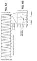
- FIG. 6A is a graphical illustration of the transfer function of a Mach-Zehnder modulator according to the present invention as a function of optical pathlength differences in wavelengths.
- FIG. 6B is a magnified view of a portion of the transfer function illustrated in FIG. 6A which illustrates the desired bias point of the Mach-Zehnder modulator in accordance with the present invention.
- FIG. 7 is a graphical illustration of a relative and differential transmission of a Mach-Zehnder modulator in accordance with the present invention as a function of the optical pathlength difference due to pre-bias, bias voltage and RF voltage signal.
- FIG. 8 is a graphical illustration of the third order two-tone spur-free dynamic range (SFDR) as a function of the biased transmission loss of the Mach-Zehnder modulator in accordance with the present invention.
- FIG. 9 is a graphical illustration of the second order two-tone SFDR as a function of the laser power mismatch.
-
- The present invention relates to an analog optical link which provides improved dynamic range as well as sensitivity. The analog optical link in accordance with the present invention includes a Mach-Zehnder optical modulator, for example as illustrated in FIG. 1. In accordance with an important aspect of the invention, the Mach-Zehnder modulator is operated at low bias points in order to improve the sensitivity and at the same time uses two optical carriers having different wavelengths with two effective bias points to cancel even ordered distortion associated with low biasing. The bias control circuit forces the two wavelengths to simultaneously bias the modulator at two bias points on opposite sides of the minimum bias point which provides equal gains with opposite signs.
- As illustrated in FIG. 4, the wavelengths may be provided by two
separate lasers lasers wave guide 48. Alternately, a single laser producing two optical carriers having different wavelengths could be used in place of the two single wavelength lasers and the WDM. The combined wavelengths are modulated with an RF input signal by way of the Mach-Zehnder modulator 20. As will be discussed in more detail below, abias control circuit 50 is provided which biases the Mach-Zehnder modulator 20 at a low bias point such that the two wavelengths have complementary small signal gains. The modulated optical signal, available at the output of the Mach-Zehnder modulator 20, may optionally be amplified with anoptical amplifier 52. Thelasers Zehnder modulator 20,bias control circuit 50,WDM 46 andoptical amplifier 52 form a transmitter portion of the optical link in accordance with the present invention. - The optical system in accordance with the present invention also includes a receiver portion which includes an optional
optical amp 54 and ademodulator 56. Thedemodulator 56 includes a wavelength division multiplexer (WDM) 58, a pair ofphotodetectors junction 64. The received signal is optically amplified by way of theoptical amplifier 54 and demultiplexed by anotherWDM 58 to produce separate wavelengths λ1 and λ2. Each wavelength λ1, λ2 is photodetected separately by thephotodetectors photodetectors junction 64 in order to provide a linearized RF output. Alternatively, the two photodetector outputs could be combined with a differential amplifier or a 180° hybrid coupler or any other device that combines the two signals 180° out of phase. - The optical transmitter and optical receiver in accordance with the present invention are coupled by an
optical link 66. Theoptical link 66 may be a fiber optic cable or waveguide based optic link or an optical link in which the modulated optical signal is transmitted in free space. Both of such embodiments are considered to be within the scope of the present invention. Theoptical link 66 could also include additional optical amplifiers distributed along the link to overcome large link losses and prevent the optical signal power from dropping too low. - As used herein, low bias is defined with reference to FIG. 5 to be a range between the quadrature bias points as indicated by the
points curve 72 and the minimum bias point indicated by thepoint 74. As shown, the transfer function of the Mach-Zehnder modulator 20 is a raised cosine function. In other words, unlike a cosine function in which the average value is 0, as seen in FIG. 5, the average value is approximately 0.5, depending on the modulator's extinction ratio. - The Mach-
Zehnder modulator 20 works on the principle of coherent interference. As discussed above, the optical input power is equally split into two arms or waveguides. The relative path lengths of these two arms can be changed. When the pathlengths are equal or differ by a multiple of the optical wavelengths, they add coherently at the output which gives maximum optical transmission. When the pathlengths differ by a multiple of the optical wavelength plus a half wavelength, they coherently cancel at the output which gives minimum optical transmission. At points in between, the signals partially cancel. - The optical pathlength difference is determined by the combination of physical path lengths plus the effective path length changes due to applied voltages, such as the bias voltage and the RF signal voltage, which change the relative index of refraction on the two arms of the modulator. For a roughly fixed optical pathlength difference, the degree of low biasing can be continuously adjusted by increasing or decreasing the wavelength separation of the lasers.
- The transfer function for a Mach-Zehnder modulator operated at two wavelengths in accordance with the present invention is illustrated in FIG. 6A. As shown, the wavelengths are 1546.1 nm as shown in solid line and 1554.1 nm, as shown in the dotted line. As shown in FIG. 6A, the difference in wavelengths provides a slight phase separation of the cosine transfer functions associated with each of the wavelengths λ1, λ2. In order to make up for the relatively poor linearity at the low bias point, the system in accordance with the present invention is operated at a bias point indicated by the
point 74. Thepoint 74 is at a point where both wavelengths λ1, λ2 have approximately equal input power but opposite slope. As shown, at the desiredbias point 74, the slope of the transfer function for one wavelength will be positive while the slope at the other wavelength will be negative as indicated in FIG. 6B. - FIG. 7 shows the benefits of the dual wavelength low bias optical link. As shown a small signal voltage (i.e. RF input signal) can swing the transfer function of the Mach-Zehnder modulator way past the minimum bias point before the link linearity has significantly degraded. The degree of cancellation of the even ordered distortions is a function of the relative matching of the optical power of the two wavelengths and their losses to the transmitter's coupled balanced detectors. Because the two wavelengths have slightly different switching voltages, the optimal laser power ratio to null even ordered distortion is not exactly one (0dB) as shown in FIG. 9. However, the calibration mismatch from 0dB is usually smaller than the calibration accuracy.
- FIGs. 8 and 9 show a comparison between single and dual wavelength Mach-Zehnder modulator based optical links. In particular, FIG. 8 shows a single wavelength link performance as a function of the degree of low biasing. The x-axis is expressed in terms of modulator optical insertion (transmission) loss due to low biasing. As shown, even with a single wavelength, the lower the biasing the better the sensitivity and the third order SFDR (assuming sufficient laser power, such that the modulator optical insertion loss does not degrade the link sensitivity). However, the second order SFDR degrades quickly as the biasing drops below quadrature (3dB bias transmission loss). As shown in FIG. 9, the dual wavelength low biased link in accordance with the present invention with a laser power mismatch of less than 0.75dB has better second order SFDR than a typical commercial quadrature biased link with passive bias control to maintain the quadrature bias.
- By choosing the bias points with opposite slopes, the output of the Mach-Zehnder modulator in accordance with the present invention will have equal modulation depth for each of the wavelengths but opposite signs. The receiver separates the two wavelengths by way of the WPM 58 (FIG. 4). Due to the opposite signs, the summing
junction 64 sums the fundamental signals coherently since their gains have opposite signs and cancels even ordered distortion since they have the same amplitude but different signs. Thephotodetectors junction 64 thus form a balanced photodetector which essentially linearizes the optical length. - The
bias control circuit 50 in accordance with the present invention is a low frequency copy of thedemodulator 56 and thus includes a WDM, (not shown) a pair of photodetectors and a summing junction (not shown). Thebias control circuit 50 is relatively simple compared to known devices and does not require dithering. In particular,bias control circuit 50 is coupled to the output of the Mach-Zehnder modulator. The DC bias voltage is adjusted in order to null the differential photocurrent. The optical losses from the laser sources to the bias control's photodetector outputs are calibrated so that thelasers demodulator 56 which adjusts the relative photocurrents to null the differential DC photocurrents. - For very high performance links requiring even better even order linearity, active bias control can be used by injecting a low frequency dither (e.g. a small 1kHz tone not shown) into the Mach-Zehnder modulator bias voltage. In this embodiment, the receiver adjusts the relative photocurrents into the summing
junction 64 in order to null the dither's second harmonic instead of the DC photocurrent with a lock-in amplifier. The photocurrents can be adjusted either by adjustable optical attenuators before eachphotodetector junction 64. The receiver must also detect the dither fundamental in order to form the reference phase for nulling the second harmonic. This configuration is similar to quadrature bias control except that the nulling circuit is on the receiver and not the transmitter. The dither enables the receiver to more accurately cancel even order distortion even when the power in the two wavelengths are not well matched in the transmitter. - Obviously, many modifications and variations of the present invention are possible in light of the above teachings. For example, the principles of the present invention may also be applied to a single wavelength intensity modulated link as a means of low bias control when multiactive operation is not required. The second wavelength is simple filtered off before the transmit
optical amplifier 52 in the transmitter. In this case, the receiver is a single photodetector with an optional optical preamplifier. The single wavelength link still has the sensitivity and third order SFDR improvements associated with low biasing. Low biased links are very sensitive to bias drift and this require active bias control. Low bias control without these two wavelength approachs is difficult to stabilize. Only the quadrature and minimum bias points are easily stabilized with a single wavelength and a single dither. Thus, it is to be understood that, within the scope of the appended claims, the invention may be practiced otherwise than as specifically described above. - What is claimed and desired to be covered by a Letters Patent is as follows:
Claims (12)
- An optical transmitter comprising:a Mach-Zehnder optical modulator having an RF input port, a bias voltage input port, an optical carrier input port and an optical output port;a wavelength division multiplexer (WDM) having two input ports and an output port, the output port coupled to said optical carrier input port of said Mach-Zehnder optical modulator; andtwo optical carrier sources having different wavelengths coupled to said input ports of said WDM.
- The optical transmitter as recited in claim 1, further including a bias control circuit coupled to said bias voltage input port.
- The transmitter as recited in claim 1, wherein said bias control circuit includes a pair of photodetectors and a wavelength division multiplexer (WDM).
- The transmitter as recited in claim 3, wherein said WDM and said pair of photodetectors are coupled to said optical output port of said Mach-Zehnder modulator.
- The optical transmitter as recited in claim 1, further including an optical amplifier coupled to said output port of said Mach-Zehnder modulator.
- An analog demodulator comprising:a wavelength division multiplexer (WDM) having an input port for receiving optical signals from a single optical link having multiple wavelengths and separating the wavelengths at its output ports;a plurality of photodetectors said photodetectors coupled to said output ports of said WDM such that each photodetector is coupled to an output port of said WDM having a different wavelength signal; anda summing junction for summing the outputs from said photodetectors.
- An optical system comprising:an optical transmitter, said optical transmitter including an optical modulator for modulating an RF input signal onto an optical carrier signal having multiple wavelengths and defining an RF modulated optical signal;an optical receiver for demodulating said RF modulated optical signal and providing an RF output signal; andan optical link connecting said optical transmitter and said optical receiver.
- The optical system as recited in claim 7, wherein said optical modulator is a Mach-Zehnder modulator having an RF input port, a bias voltage input port, an optical carrier input port, and an optical output port.
- The optical system as recited in claim 8, wherein said optical transmitter includes a wavelength division multiplexer (WDM) and said optical carrier signal having multiple wavelengths is formed from a plurality of carrier signals having different wavelengths for providing an optical carrier signal to said optical carrier input port of said Mach-Zehnder modulator, said optical transmitter also including a plurality of sources of carrier signals at different wavelengths which are applied to said WDM.
- An optical transmitter comprising:a Mach-Zehnder optical modulator having an RF input port, a bias voltage input port, an optical carrier input port and an optical carrier output port; andmeans for providing two optical sources having different wavelengths.
- The optical transmitter as recited in claim 10, wherein said providing means includes a single laser which produces two optical carriers having different wavelengths.
- The optical transmitter as recited in claim 10, wherein said providing means includes a wavelength division multiplexer and two optical carrier sources.
Applications Claiming Priority (2)
| Application Number | Priority Date | Filing Date | Title |
|---|---|---|---|
| US09/322,283 US7079780B1 (en) | 1999-05-28 | 1999-05-28 | Linearized optical link using a single Mach-Zehnder modulator and two optical carriers |
| US322283 | 1999-05-28 |
Publications (2)
| Publication Number | Publication Date |
|---|---|
| EP1056228A2 true EP1056228A2 (en) | 2000-11-29 |
| EP1056228A3 EP1056228A3 (en) | 2004-11-03 |
Family
ID=23254196
Family Applications (1)
| Application Number | Title | Priority Date | Filing Date |
|---|---|---|---|
| EP00110950A Withdrawn EP1056228A3 (en) | 1999-05-28 | 2000-05-25 | Linearized optical link using a single Mach-Zender modulator and two optical carriers |
Country Status (3)
| Country | Link |
|---|---|
| US (1) | US7079780B1 (en) |
| EP (1) | EP1056228A3 (en) |
| JP (1) | JP3337458B2 (en) |
Cited By (14)
| Publication number | Priority date | Publication date | Assignee | Title |
|---|---|---|---|---|
| WO2002091645A1 (en) * | 2001-05-10 | 2002-11-14 | Fujitsu Limited | Method and system for demultiplexing non-intensity modulated wavelength division multiplexed (wdm) signals |
| WO2002091644A1 (en) * | 2001-05-10 | 2002-11-14 | Fujitsu Limited | Receiver and method of receiving a multichannel optical signal |
| WO2003007444A1 (en) * | 2001-07-12 | 2003-01-23 | Textron Systems Corporation | Semiconductor zigzag laser and optical amplifier |
| US7200338B2 (en) | 2001-05-10 | 2007-04-03 | Fujitsu Limited | Method and system for communicating a clock signal over an optical link |
| US7433376B1 (en) | 2006-08-07 | 2008-10-07 | Textron Systems Corporation | Zig-zag laser with improved liquid cooling |
| US7852082B2 (en) | 2005-03-29 | 2010-12-14 | General Electric Company | Remote monitoring system and method |
| WO2013112537A1 (en) * | 2012-01-24 | 2013-08-01 | Harris Corporation | Communications device with discriminator for generating intermediate frequency signal and related methods |
| US8620158B2 (en) | 2012-01-24 | 2013-12-31 | Harris Corporation | Communications device with discriminator and wavelength division multiplexing for generating intermediate frequency signal and related methods |
| WO2014016461A1 (en) * | 2012-07-24 | 2014-01-30 | Das Photonics, S.L. | System for establishing an analog optical fiber link with a high dynamic range for high frequencies |
| US8879919B2 (en) | 2011-09-09 | 2014-11-04 | Harris Corporation | Photonic communications device with an FM/PM discriminator and related methods |
| US8995480B2 (en) | 2012-03-14 | 2015-03-31 | Electronics And Telecommunications Research Institute | Tunable laser module |
| CN105933072A (en) * | 2016-04-07 | 2016-09-07 | 北京邮电大学 | Device for simulating optical link linearization |
| US9698913B2 (en) | 2014-06-06 | 2017-07-04 | The John Hopkins University | System and method for distortion correction in phase-encoded photonic links |
| GB2588502A (en) * | 2019-08-13 | 2021-04-28 | Leonardo Mw Ltd | A system and method for increasing optical power in an RF over fibre link |
Families Citing this family (27)
| Publication number | Priority date | Publication date | Assignee | Title |
|---|---|---|---|---|
| US7016555B2 (en) * | 2003-03-19 | 2006-03-21 | Optimer Photonics, Inc. | Electrooptic modulators and waveguide devices incorporating the same |
| CN1306736C (en) * | 2003-06-13 | 2007-03-21 | 松下电器产业株式会社 | System, device, and method for radio frequency optical transmission |
| ITTO20030708A1 (en) * | 2003-09-16 | 2005-03-17 | Istituto Superiore Mario Boella Sul Le Tecnologie | OPTICAL OSCILLATOR CONTROLLED IN VOLTAGE FOR A RING |
| US7359580B2 (en) * | 2005-07-25 | 2008-04-15 | University Of Victoria Innovation And Development Corporation | Class-AB microwave-photonic link |
| US7369715B2 (en) * | 2005-08-22 | 2008-05-06 | University Of Victoria Innovation And Development Corporation | Photonic link using angle modulation and method of use thereof |
| US8249460B2 (en) * | 2007-06-22 | 2012-08-21 | Lockheed Martin Corporation | Apparatus and method for generating an RF signal |
| US8260143B2 (en) | 2008-03-12 | 2012-09-04 | Hypres, Inc. | Digital radio frequency tranceiver system and method |
| US8150270B2 (en) * | 2008-03-31 | 2012-04-03 | Kitel Technologies Llc | Compact high-speed modulator driver method and apparatus |
| US8103178B2 (en) * | 2008-04-18 | 2012-01-24 | The United States Of America As Represented By The Secretary Of The Navy | Linearized phase modulated analog optical links |
| US8693875B2 (en) * | 2008-11-20 | 2014-04-08 | Applied Communications Sciences | Method and apparatus for optimized analog RF optical links |
| US8224188B2 (en) * | 2009-04-21 | 2012-07-17 | The United States Of America, As Represented By The Secretary Of The Navy | Even-order harmonic cancellation and increased RF gain using dual-output mach-zehnder modulator with two wavelength input |
| US8674870B2 (en) | 2011-01-19 | 2014-03-18 | Photonic Systems, Inc. | Methods and apparatus for active reflection |
| CN102884738B (en) * | 2011-04-20 | 2015-04-08 | 华为技术有限公司 | Signal reception device and method based on microwave photon technology |
| US8908187B2 (en) | 2011-11-02 | 2014-12-09 | Honeywell International Inc. | System and method for reducing errors in a resonator fiber optic gyroscope |
| DE102011086561B4 (en) * | 2011-11-17 | 2013-06-13 | Siemens Aktiengesellschaft | MRI system, receiving device for an MRI system and method for obtaining an MR signal in an MRI system |
| CN102624460B (en) * | 2012-01-16 | 2014-09-10 | 北京大学 | Modulator for optical fibre linear transmission and third-order intermodulation suppression method for modulator |
| US8824901B2 (en) * | 2012-03-29 | 2014-09-02 | The United States Of America, As Represented By The Secretary Of The Navy | Multi-mode optoelectronic oscillator |
| US8849129B2 (en) * | 2012-07-20 | 2014-09-30 | Finisar Corporation | Method and apparatus for stabilization of optical transmitter |
| US9172471B2 (en) * | 2013-03-15 | 2015-10-27 | The United States Of America, As Represented By The Secretary Of The Navy | System and method for suppression of even-order photodiode distortions |
| US9485012B2 (en) * | 2014-10-15 | 2016-11-01 | Infinera Corporation | Optical link protection using common modulation of multiple combined wavelengths |
| CN104702339A (en) * | 2014-12-10 | 2015-06-10 | 北京邮电大学 | Method and device for simulating optical link linearization |
| US9683846B2 (en) | 2015-11-23 | 2017-06-20 | Honeywell International Inc. | Resonator fiber optic gyroscope resonance detection demodulator reference phase corrector |
| CN105790840B (en) * | 2016-05-13 | 2018-01-12 | 南京大学 | Broadband analog signal linearizes fibre-optic transmission system (FOTS) |
| US10341031B2 (en) * | 2017-04-10 | 2019-07-02 | The Government Of The United States Of America, As Represented By The Secretary Of The Navy | Reduction of photodiode nonlinearities by adaptive biasing |
| FR3078598B1 (en) * | 2018-03-01 | 2020-02-07 | Thales | DUAL BAND FREQUENCY CONVERSION PHOTONIC DEVICE AND METHOD |
| US11404596B1 (en) * | 2021-04-20 | 2022-08-02 | Ciena Corporation | Balancing a pair of avalanche photodiodes in a coherent receiver |
| CN113422650A (en) * | 2021-06-25 | 2021-09-21 | 中国科学院半导体研究所 | Multichannel optical frequency hopping system, signal encryption method and optical communication equipment |
Citations (3)
| Publication number | Priority date | Publication date | Assignee | Title |
|---|---|---|---|---|
| US5031235A (en) * | 1989-10-27 | 1991-07-09 | Hoechst Celanese Corp. | Cable system incorporating highly linear optical modulator |
| US5940196A (en) * | 1997-05-16 | 1999-08-17 | Harmonic Lightwaves, Inc. | Optical communications system with wavelength division multiplexing |
| WO2000018044A1 (en) * | 1998-09-18 | 2000-03-30 | Massachusetts Institute Of Technology | Linearization of a broadband analog link using two wavelengths |
Family Cites Families (20)
| Publication number | Priority date | Publication date | Assignee | Title |
|---|---|---|---|---|
| US5119447A (en) | 1990-11-06 | 1992-06-02 | General Instrument Corporation | Apparatus and method for externally modulating an optical carrier |
| US5227857A (en) | 1991-04-24 | 1993-07-13 | The United States Of America As Represented By The Secretary Of The Navy | System for cancelling phase noise in an interferometric fiber optic sensor arrangement |
| US5257124A (en) * | 1991-08-15 | 1993-10-26 | General Instrument Corporation | Low distortion laser system for AM fiber optic communication |
| JP3019284B2 (en) * | 1992-08-10 | 2000-03-13 | シャープ株式会社 | Spatial optical transmission equipment |
| JP3226067B2 (en) * | 1992-10-03 | 2001-11-05 | キヤノン株式会社 | Optical communication method and optical communication system |
| US5710653A (en) * | 1995-03-06 | 1998-01-20 | Fiber Optic Network Solutions Corp. | Linear multi-output optical transmitter system |
| US5870216A (en) | 1995-10-26 | 1999-02-09 | Trw Inc. | Splitterless optical broadcast switch |
| US5661582A (en) * | 1995-10-26 | 1997-08-26 | Trw Inc. | Photonic interconnect and photonic processing for communications and data handling satellites |
| GB9604303D0 (en) * | 1996-02-29 | 1996-05-01 | Stc Submarine Systems Ltd | Chromatic pre-chip in NRZ transmitter |
| US5953139A (en) * | 1996-03-06 | 1999-09-14 | Cfx Communications Systems, Llc | Wavelength division multiplexing system |
| US6252692B1 (en) * | 1996-06-07 | 2001-06-26 | Nortel Networks Limited | Optical fibre transmission systems |
| CA2188358A1 (en) * | 1996-10-21 | 1998-04-21 | Michael J. Sieben | optical modulation system |
| US5917638A (en) * | 1997-02-13 | 1999-06-29 | Lucent Technologies, Inc. | Duo-binary signal encoding |
| US6188497B1 (en) * | 1997-02-13 | 2001-02-13 | Lucent Technologies Inc. | Duo-binary signal encoding |
| US5864625A (en) * | 1997-03-17 | 1999-01-26 | At&T Corp | Methods and apparatus for secure optical communications links |
| US5917179A (en) * | 1997-05-12 | 1999-06-29 | California Institute Of Technology | Brillouin opto-electronic oscillators |
| US6229632B1 (en) * | 1997-05-12 | 2001-05-08 | Ditech Corporation | Broadband optical transmission system utilizing differential wavelength modulation |
| US5995256A (en) * | 1997-09-30 | 1999-11-30 | Mci Communications Corporation | Method and system for managing optical subcarrier reception |
| US5917970A (en) * | 1998-04-21 | 1999-06-29 | The United States Of America As Represented By The Secretary Of The Navy | Wavelength multiplexed, electro-optically controllable, fiber optic multi-tap delay line |
| US6271953B1 (en) * | 1998-09-02 | 2001-08-07 | Harris Corporation | Method and system for optical free space communications using non-mechanical beam steering |
-
1999
- 1999-05-28 US US09/322,283 patent/US7079780B1/en not_active Expired - Fee Related
-
2000
- 2000-05-24 JP JP2000152370A patent/JP3337458B2/en not_active Expired - Fee Related
- 2000-05-25 EP EP00110950A patent/EP1056228A3/en not_active Withdrawn
Patent Citations (3)
| Publication number | Priority date | Publication date | Assignee | Title |
|---|---|---|---|---|
| US5031235A (en) * | 1989-10-27 | 1991-07-09 | Hoechst Celanese Corp. | Cable system incorporating highly linear optical modulator |
| US5940196A (en) * | 1997-05-16 | 1999-08-17 | Harmonic Lightwaves, Inc. | Optical communications system with wavelength division multiplexing |
| WO2000018044A1 (en) * | 1998-09-18 | 2000-03-30 | Massachusetts Institute Of Technology | Linearization of a broadband analog link using two wavelengths |
Cited By (18)
| Publication number | Priority date | Publication date | Assignee | Title |
|---|---|---|---|---|
| WO2002091645A1 (en) * | 2001-05-10 | 2002-11-14 | Fujitsu Limited | Method and system for demultiplexing non-intensity modulated wavelength division multiplexed (wdm) signals |
| WO2002091644A1 (en) * | 2001-05-10 | 2002-11-14 | Fujitsu Limited | Receiver and method of receiving a multichannel optical signal |
| EP1548967A1 (en) * | 2001-05-10 | 2005-06-29 | Fujitsu Limited | Method and system for demultiplexing non-intensity modulated wavelength division multiplexed (WDM) signals |
| US7035543B1 (en) | 2001-05-10 | 2006-04-25 | Fujitsu Limited | Method and system for demultiplexing non-intensity modulated wavelength division multiplexed (WDM) signals |
| US7200338B2 (en) | 2001-05-10 | 2007-04-03 | Fujitsu Limited | Method and system for communicating a clock signal over an optical link |
| US7200344B1 (en) | 2001-05-10 | 2007-04-03 | Fujitsu Limited | Receiver and method for a multichannel optical communication system |
| WO2003007444A1 (en) * | 2001-07-12 | 2003-01-23 | Textron Systems Corporation | Semiconductor zigzag laser and optical amplifier |
| US7852082B2 (en) | 2005-03-29 | 2010-12-14 | General Electric Company | Remote monitoring system and method |
| US7433376B1 (en) | 2006-08-07 | 2008-10-07 | Textron Systems Corporation | Zig-zag laser with improved liquid cooling |
| US8879919B2 (en) | 2011-09-09 | 2014-11-04 | Harris Corporation | Photonic communications device with an FM/PM discriminator and related methods |
| WO2013112537A1 (en) * | 2012-01-24 | 2013-08-01 | Harris Corporation | Communications device with discriminator for generating intermediate frequency signal and related methods |
| US8620158B2 (en) | 2012-01-24 | 2013-12-31 | Harris Corporation | Communications device with discriminator and wavelength division multiplexing for generating intermediate frequency signal and related methods |
| US8995480B2 (en) | 2012-03-14 | 2015-03-31 | Electronics And Telecommunications Research Institute | Tunable laser module |
| WO2014016461A1 (en) * | 2012-07-24 | 2014-01-30 | Das Photonics, S.L. | System for establishing an analog optical fiber link with a high dynamic range for high frequencies |
| US9698913B2 (en) | 2014-06-06 | 2017-07-04 | The John Hopkins University | System and method for distortion correction in phase-encoded photonic links |
| CN105933072A (en) * | 2016-04-07 | 2016-09-07 | 北京邮电大学 | Device for simulating optical link linearization |
| GB2588502A (en) * | 2019-08-13 | 2021-04-28 | Leonardo Mw Ltd | A system and method for increasing optical power in an RF over fibre link |
| GB2588502B (en) * | 2019-08-13 | 2022-12-14 | Leonardo UK Ltd | A system and method for increasing optical power in an RF over fibre link |
Also Published As
| Publication number | Publication date |
|---|---|
| JP2000356759A (en) | 2000-12-26 |
| JP3337458B2 (en) | 2002-10-21 |
| US7079780B1 (en) | 2006-07-18 |
| EP1056228A3 (en) | 2004-11-03 |
Similar Documents
| Publication | Publication Date | Title |
|---|---|---|
| US7079780B1 (en) | Linearized optical link using a single Mach-Zehnder modulator and two optical carriers | |
| EP0403991B1 (en) | Optical distribution of analog and digital signals using optical modulators with complementary outputs | |
| US6246500B1 (en) | Linearization of a broadband analog optical link using two wavelengths | |
| US6304369B1 (en) | Method and apparatus for eliminating noise in analog fiber links | |
| US5031235A (en) | Cable system incorporating highly linear optical modulator | |
| US4860279A (en) | Source modulated coherence multiplexed optical signal transmission system | |
| US5532857A (en) | Wide dynamic range optical link using DSSC linearizer | |
| US7657130B2 (en) | Silicon-based optical modulator for analog applications | |
| US6616353B1 (en) | Laser intensity noise suppression using unbalanced interferometer modulation | |
| WO2012165656A1 (en) | Optical waveguide device, optical interferometer, and method for producing optical waveguide device | |
| EP3488291B1 (en) | Inherently broadband linearized electro-optic modulator with customizable performance | |
| JPH0799478A (en) | Apparatus and method for distributed compensation of fiber optic transmission system | |
| US8849114B2 (en) | Nonlinear compensation in WDM systems | |
| JPH08274415A (en) | Photon diplexer device | |
| US9746742B2 (en) | Electro-optic modulator with distributed gain | |
| US10715258B1 (en) | Optical coherent receiver | |
| US10120127B1 (en) | Multi-element optical links | |
| US8170422B2 (en) | Frequency shift keying demodulator | |
| Naughton et al. | Error-free 10Gb/s duobinary transmission over 215km of SSMF using a hybrid photonic integrated reflective modulator | |
| Dong et al. | Photonic integration | |
| US9768877B2 (en) | Multi-bit digital to analog-optical converter | |
| Achiam et al. | Systems with higher-order modulation | |
| Doerr et al. | Optical dispersion compensator suitable for use with non-wavelength-locked transmitters | |
| Doerr | Compact advanced modulation format InP modulators and receivers | |
| Mašanović et al. | CASOPIS REPUBLICKE AGENCIJE ZA TELEKOMUNIKACIJE |
Legal Events
| Date | Code | Title | Description |
|---|---|---|---|
| PUAI | Public reference made under article 153(3) epc to a published international application that has entered the european phase |
Free format text: ORIGINAL CODE: 0009012 |
|
| AK | Designated contracting states |
Kind code of ref document: A2 Designated state(s): AT BE CH CY DE DK ES FI FR GB GR IE IT LI LU MC NL PT SE |
|
| AX | Request for extension of the european patent |
Free format text: AL;LT;LV;MK;RO;SI |
|
| RAP1 | Party data changed (applicant data changed or rights of an application transferred) |
Owner name: NORTHROP GRUMMAN CORPORATION |
|
| RAP1 | Party data changed (applicant data changed or rights of an application transferred) |
Owner name: NORTHROP GRUMMAN CORPORATION |
|
| PUAL | Search report despatched |
Free format text: ORIGINAL CODE: 0009013 |
|
| AK | Designated contracting states |
Kind code of ref document: A3 Designated state(s): AT BE CH CY DE DK ES FI FR GB GR IE IT LI LU MC NL PT SE |
|
| AX | Request for extension of the european patent |
Extension state: AL LT LV MK RO SI |
|
| 17P | Request for examination filed |
Effective date: 20050404 |
|
| AKX | Designation fees paid |
Designated state(s): DE FR GB IT |
|
| 17Q | First examination report despatched |
Effective date: 20071219 |
|
| STAA | Information on the status of an ep patent application or granted ep patent |
Free format text: STATUS: THE APPLICATION IS DEEMED TO BE WITHDRAWN |
|
| 18D | Application deemed to be withdrawn |
Effective date: 20080430 |