EP1065626A1 - Chip card memory management for power saving modes in a mobile phone - Google Patents
Chip card memory management for power saving modes in a mobile phone Download PDFInfo
- Publication number
- EP1065626A1 EP1065626A1 EP00401707A EP00401707A EP1065626A1 EP 1065626 A1 EP1065626 A1 EP 1065626A1 EP 00401707 A EP00401707 A EP 00401707A EP 00401707 A EP00401707 A EP 00401707A EP 1065626 A1 EP1065626 A1 EP 1065626A1
- Authority
- EP
- European Patent Office
- Prior art keywords
- smart card
- information
- memory
- message
- micromodule
- Prior art date
- Legal status (The legal status is an assumption and is not a legal conclusion. Google has not performed a legal analysis and makes no representation as to the accuracy of the status listed.)
- Granted
Links
Images

Classifications
-
- G—PHYSICS
- G06—COMPUTING; CALCULATING OR COUNTING
- G06K—GRAPHICAL DATA READING; PRESENTATION OF DATA; RECORD CARRIERS; HANDLING RECORD CARRIERS
- G06K19/00—Record carriers for use with machines and with at least a part designed to carry digital markings
- G06K19/06—Record carriers for use with machines and with at least a part designed to carry digital markings characterised by the kind of the digital marking, e.g. shape, nature, code
- G06K19/067—Record carriers with conductive marks, printed circuits or semiconductor circuit elements, e.g. credit or identity cards also with resonating or responding marks without active components
- G06K19/07—Record carriers with conductive marks, printed circuits or semiconductor circuit elements, e.g. credit or identity cards also with resonating or responding marks without active components with integrated circuit chips
- G06K19/073—Special arrangements for circuits, e.g. for protecting identification code in memory
-
- G—PHYSICS
- G06—COMPUTING; CALCULATING OR COUNTING
- G06K—GRAPHICAL DATA READING; PRESENTATION OF DATA; RECORD CARRIERS; HANDLING RECORD CARRIERS
- G06K7/00—Methods or arrangements for sensing record carriers, e.g. for reading patterns
- G06K7/0008—General problems related to the reading of electronic memory record carriers, independent of its reading method, e.g. power transfer
-
- H—ELECTRICITY
- H04—ELECTRIC COMMUNICATION TECHNIQUE
- H04W—WIRELESS COMMUNICATION NETWORKS
- H04W52/00—Power management, e.g. TPC [Transmission Power Control], power saving or power classes
- H04W52/02—Power saving arrangements
- H04W52/0209—Power saving arrangements in terminal devices
-
- Y—GENERAL TAGGING OF NEW TECHNOLOGICAL DEVELOPMENTS; GENERAL TAGGING OF CROSS-SECTIONAL TECHNOLOGIES SPANNING OVER SEVERAL SECTIONS OF THE IPC; TECHNICAL SUBJECTS COVERED BY FORMER USPC CROSS-REFERENCE ART COLLECTIONS [XRACs] AND DIGESTS
- Y02—TECHNOLOGIES OR APPLICATIONS FOR MITIGATION OR ADAPTATION AGAINST CLIMATE CHANGE
- Y02D—CLIMATE CHANGE MITIGATION TECHNOLOGIES IN INFORMATION AND COMMUNICATION TECHNOLOGIES [ICT], I.E. INFORMATION AND COMMUNICATION TECHNOLOGIES AIMING AT THE REDUCTION OF THEIR OWN ENERGY USE
- Y02D30/00—Reducing energy consumption in communication networks
- Y02D30/70—Reducing energy consumption in communication networks in wireless communication networks
Definitions
- the subject of the present invention is a method for managing a power consumption of a smart card in a mobile phone.
- the object of the invention is to increase the autonomy of a mobile telephone provided of such a smart card.
- phase 2 smart cards for such mobile phones by in relation to functions that they are capable of performing. So, we distinguish first of all phase 2 smart cards called SIM cards phase 2 (for Subscriber Identity Module in English, Subscriber Identity Module in English French). Compared to a phase 1, a phase 2 smart card is a card chip which performs only sophisticated functions secure calculation and data control. She also realizes functions of memorization in an internal memory. In addition, a card puce phase 2 can only send information to the mobile phone if it was authorized by the latter. An evolution of phase smart cards 2 led to phase 2+ smart cards known as phase 2+ SIM cards or SIM cards toolkit. A phase 2+ smart card is capable, unlike a phase 2 smart card, to send commands to a mobile phone. Generally, these so-called proactive commands allow a card to smart to manage man / machine dialogs between a phone mobile and a user of this mobile phone, in particular by using a screen and / or keyboard of this mobile phone as a dialogue interface.
- the invention applies more particularly to phase smart cards 2+.
- the object of the invention is to allow consumption management of these phase 2+ smart cards without loss of information.
- phase 2 smart cards can be put on standby at any time. Indeed, a standby is done by order of the mobile phone. Generally, a stake standby is performed after the phase 2 smart card has finished a task controlled by mobile phone.
- phase 2+ smart card can produce orders.
- an architecture of such a smart card comprises in particular, in addition to a microprocessor and a non-volatile memory of EEPROM type, a volatile RAM read and write memory.
- This RAM memory has the function of temporarily keeping in memory a work context necessary to subsequently produce, in particular proactive orders.
- a power cut to the smart card phase 2+ by mobile phone, as in the state of the technique leads to immediate loss of memory information RAM. This is not acceptable since a standby command occurs done without acknowledgment of the smart card. We lose all data that are being used or that were going to be used and that have not been saved in a memory other than in the RAM memory of the phase smart card 2+.
- the object of the present invention is to remedy these problems by proposing a method for managing an electrical consumption of a card smart.
- a method for managing an electrical consumption of a card smart With the method of the invention, one checks, before placing it in a standby state, characteristics of the smart card inserted in the mobile phone and it is determined whether there should be a possible backup, in this case we also determine a backup location, or not.
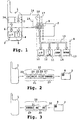
- Figure 1 shows in schematic form a telephone 1 mobile with a smart card 2.
- Phone 1 has a microprocessor 3 controlled by a program 4 in a memory of programs 5 with a bus 6 of data, addresses and commands.
- the telephone 1 further comprises a supply device 7.
- Map 2 has a micromodule 8.
- the micromodule 8 has a connector 9, a microprocessor 10 controlled by a program 11 in a memory of programs 12, a non-volatile memory 13 of EEPROM type (Electrically Erasable Read Only Memory in English, reading memory only electrically erasable programmable in French), a memory 14 RAM type (Random Access Memory in English, access memory random in French but we prefer the expression volatile memory) and a bus 15 for data, addresses and commands.
- EEPROM Electrically Erasable Read Only Memory
- memory 14 RAM type Random Access Memory in English, access memory random in French but we prefer the expression volatile memory
- Connector 9 allows an electrical connection between bus 6 of telephone 1 and bus 15 of card 2.
- Connector 9 has several metal pins, one of which is connected by a metal link 16 to the device 7. Obviously, to be able to provide food.
- An electrical connection between the device 7 and card 2 must have two links. A first bond is formed by link 16 and the other link, the one fixed to a reference potential of the device 7, is not described so as not to burden the description.
- an electrical continuity of the link 16 between the device 7 and the connector 9 is provided by a switch 17 including an input 18 of control is connected to bus 6 by a link 19.
- An opening or a closing of the switch 17 is controlled by the microprocessor 3 with the program 4.
- a module 8 of a card 2 of the type is considered.
- phase 2+ which compared to a phase 2 smart card allows sending to a phone 1 orders.
- Micromodule 8 can send over the phone 1 a number of possible commands different from another micromodule 8.
- micromodule 8 must keep in permanence in memory 14 of information useful for managing applications controlled by micromodule 8.
- telephone 1 and the micromodule exchange information using a communication protocol defined in ISO7816-3.
- ISO7816-3 a communication protocol defined in ISO7816-3.
- This standard provides that an exchange of information with telephone 1 and micromodule 8 takes place always on the initiative of the telephone 1.
- a message of command and a response message we define a message of command and a response message.
- FIG. 2 shows an example of a structure of a message 20 of command sent to micromodule 8 by telephone 1.
- This message 20 has a header 21 and an optional data field 22.
- Header 21 has five fields 23 to 27 of one byte each.
- Field 23 receives a value specifying an application type.
- Field 24 receives a value specifying the instruction to be executed.
- Field 25 and field 26 receive values used to specify parameters of the instruction defined in the field 24.
- the values in field 25 and field 26 are optional.
- the field 27 receives a value allowing to give the length in bit either of message 20 is an expected response message.
- a length in bit of field 22 is variable, and receives a value corresponding to a data useful to micromodule 8 for carrying out the instruction placed in the field 24.
- the micromodule 8 of the card 2 sends on telephone 1, in FIG. 3, a response message 28.
- Message 28 has a data field 29 and an epilogue 30.
- the epilogue 30 has a field 31 and a field 32 of one byte each.
- a value received in field 31 and / or 32 indicates whether the instruction sent by the message 20 (figure 2) was executed correctly or not.
- Generally worth received in field 31 represents a correct execution or an execution instruction incorrect and a value received in field 32 represents generally, upon incorrect execution of the instruction, a cause of the encountered problem.
- Field 29, like field 22, is optional.
- communication from telephone 1 to the micromodule 8 is always done by breaking down a message to be sent such as message 20.
- communication from micromodule 8 to the phone 1 is always done by decomposing a message sent such as the message 28.
- the micromodule 8 when sending a message 28, places it in the field 31 a special value.
- This special value is generally equal to 90 in a hexadecimal representation and indicates on the telephone1 that the micromodule 8 wants to send an order.
- phone 1 sends a message 20 to micromodule 8 including a content of field 24 indicates to micromodule 8 that it can issue its command in using a message 28 for which field 29 is present. In that case, we place in field 29 a value representative of the command that the micromodule 8 wants to send to phone 1, this command being the most often called proactive control.
- the telephone 1 sends the micromodule 8 a message 20.
- This message 20 indicates to the micromodule 8 in particular by means of field 22, which proactive commands the telephone 1 can receive, the other proactive commands available in the micromodule 8 cannot be interpreted by the microprocessor 3.
- the micromodule 8 sends to the microprocessor 3 a message 28 representing an identification message of the micromodule 8.
- the micromodule 8 indicates to the microprocessor 3 whether the micromodule 8 can manage internal standby or not. Such management mainly consists in saving the context present in the memory 14.
- the identification message can be sent to the telephone 1 in different ways.
- the identification message is placed in the field 31 of the message 28.
- the telephone 1 sends a new message 20 to the micromodule 8 in order to authorize the micromodule 8 to respond.
- the response of micromodule 8 is placed in field 29 of message 28.
- an identification message has a length of two bits.
- the microprocessor 3 reads the two corresponding bits, which will hereinafter be called B 0 and B 1 , from the field 31 of the message 28.
- a logical value of the bits B 0 and B 1 is either a value logic 0 is a logical value 1.
- FIG. 4 shows, in the form of an algorithm, an operation of the method of the invention.
- the telephone 1 sends a so-called TERMINAL PROFILE information message to the micromodule 8 using a message 20 and the micromodule 8 returns an identification message in response using a message 28.
- the microprocessor 3 reads the B bits 0 and B 1 of field 31 of message 28 received. These bits B 0 and B 1 are coded, for example, as follows. A logical value of the bits Bo and B 1 equal to 0 indicates that the program 11 of the micromodule 8 does not manage an opening of the switch 17. It is generally a smart card phase 2 or an earlier version .
- a logical value of the bit Bo equal to 1 and a logical value of the bit B 1 equal to 0 indicates that the program 11 can manage an opening of the switch 17 and therefore a backup of the present context but that it must use a memory of backup external to micromodule 8.
- the telephone 1 has a memory 34 for saving information relating to micromodule 8.
- a logical value of bit B 0 equal to 0 and a logical value of bit B 1 equal to 1 indicates that program 11 can manage, internally, a backup of the context present in the memory 14 by using the memory 13 of the micromodule 8.
- the program 11 does not know how to manage externally, that is to say with the memory 34 of telephone 1, a backup of the context.
- a logical value of bit B 0 and bit B 1 equal to 1 indicates that the program 11 can manage a backup of the context both internally with memory 13 and externally with memory 34.
- a test step 35 the microprocessor 3 tests whether at least one of the two bits B 0 or B 1 has a logical value equal to 1. In the case of a negative response to this test, this means that the micromodule 8 does not know not handle a power cut. Consequently, the switch 17 can be controlled, in a step 36, upon opening by the microprocessor 3.
- a test step 37 is then carried out in which one waits for the telephone 1 to want to send the micromodule 8 a request for standby.
- the microprocessor 3 performs a test of a logical value of each bit B 0 and B 1 in a step 38.
- the microprocessor 3 compares the bits B 0 and B 1 with logical values 1 and 0 respectively. In the case where the logical values of the bits B 0 and B 1 are equal to the compared logical values then, in a step 39, the telephone 1 sends to the micromodule 8 a message 20 corresponding to a request for standby.
- the backup location in field 25, information on the location of the backup.
- the backup location must be memory 34.
- a value in field 25 to indicate that a backup location corresponds to memory 34 is equal to the decimal value one.
- the microprocessor 3 performs, in a step 40, a comparison between logical values of bits B 0 and B 1 and logical values 0 and 1 respectively. In the case where the logical values of the bits B 0 and B 1 correspond to the compared values, this means that the program 11 of the micromodule 8 can internally manage an opening of the switch 17.
- the telephone 1 in a step 41 , sends to micromodule 8 a request for standby by coding in field 25 of message 20 information indicating that the place of saving corresponds to memory 13.
- a code for the message of step 41 is different from the code for the message from step 39, for example you can assign a decimal value equal to zero.
- the program 11 can manage an opening of the switch 17 either internally either externally.
- an information code of the place of backup is equal to either the decimal zero or the decimal one.
- the program 11, in a preferred example manages an opening of the switch 17 internally, that is to say that it uses the memory 13 of the micromodule 8.
- the field 25 of message 20 we used the field 25 of message 20 but we could very well have used other fields such as field 26 or field 22 or even a combination of these fields. Values chosen to code this location information backup in steps 39, 41 and 42 is free as long as they allow distinguish a backup location.
- the microprocessor 10 reads, in field 25, a value of the information of the place of saving. This backup is done either in memory 13 or in memory 34 in depending on the value present in field 25. If a backup location is memory 34, microprocessor 10 sends to phone 1 every data to be backed up. When a backup location corresponds to memory 13 the microprocessor does not send any message to telephone 1. Once the backup has been made, the microprocessor 3 controls the opening of switch 17.
- the telephone mobile waits for an acknowledgment from micromodule 8 before opening switch 17. This wait can be delayed. The flow of this timeout without response can be considered a response.
- the microprocessor 3 reads the acknowledgment message sent by micromodule 8 or take this answer into account and then command the opening of the switch 17 using the link 19 connected to the bus 6.
- a step 44 the microprocessor 3 controls a standby time of the micromodule 8.
- the microprocessor 3 controls, in a step 45, as a function of the logical values of the bits B 0 and B 1 the place for saving the information which was present in the memory 14 before the standby.
- the microprocessor 3 sends a message 20 comprising the field 22.
- the values of the information stored in the memory 34 are placed in the field 22.
- the microprocessor 10 when the micromodule 8 receives the message 20, stores the information present in the field 22 of the message 20 in the memory 14.
- the microprocessor 10 thus returns, in a step 47, the micromodule 8 to the state it was in before standby.
- the test in step 46 indicates that the backup has been performed internally in the memory 13, then the microprocessor 3 does not send the message 20 from step 47 to the micromodule 8.
- a memory for example the memory 13, of micromodule 8 information relating to a key of encryption and an associated encryption algorithm. So during a backup external in memory 34 program 11 uses this algorithm encryption and this encryption key to encrypt present information in memory 14 before placing them on bus 6. We thus render these unusable data outside the micromodule 8. The microprocessor 3 then places this encrypted data in memory 34. During a reverse operation, i.e. recovery of encrypted information in memory 34, after step 17 in particular, the program 11 uses to new encryption algorithm and encryption key to decrypt data received before storing it in memory 14.
Abstract
Description
La présente invention a pour objet un procédé de gestion d'une consommation électrique d'une carte à puce dans un téléphone mobile. Le but de l'invention est d'augmenter l'autonomie d'un téléphone mobile muni d'une telle carte à puce.The subject of the present invention is a method for managing a power consumption of a smart card in a mobile phone. The object of the invention is to increase the autonomy of a mobile telephone provided of such a smart card.
On différencie des cartes à puce pour de tels téléphones mobiles par
rapport à des fonctions qu'elles sont capables de réaliser. Ainsi, on distingue
tout d'abord des cartes à puce phase 2 dites cartes SIM phase 2 (pour
Subscriber Identity Module en anglais, module d'identité d'abonné en
français). Par rapport à une phase 1, une carte à puce phase 2 est une carte
à puce qui réalise, de manière perfectionnée, seulement des fonctions
sécurisées de calcul et de contrôle de données. Elle réalise aussi des
fonctions de mémorisation dans une mémoire interne. De plus, une carte à
puce phase 2 ne peut envoyer des informations au téléphone mobile que si
elle y a été autorisée par ce dernier. Une évolution des cartes à puce phase
2 a conduit aux cartes à puce phase 2+ dites cartes SIM phase 2+ ou encore
cartes SIM toolkit. Une carte à puce phase 2+ est capable, à l'inverse d'une
carte à puce phase 2, d'envoyer des commandes à un téléphone mobile.
Généralement, ces commandes dites pro-actives permettent à une carte à
puce de gérer des dialogues de type homme/machine entre un téléphone
mobile et un utilisateur de ce téléphone mobile en utilisant notamment un
écran et/ou un clavier de ce téléphone mobile comme interface de dialogue.We differentiate smart cards for such mobile phones by
in relation to functions that they are capable of performing. So, we distinguish
first of all
L'invention s'applique plus particulièrement aux cartes à puce phase
2+. Le but de l'invention est de permettre une gestion de la consommation
électrique de ces cartes à puce phase 2+ sans perte d'informations.The invention applies more particularly to phase
Actuellement, des procédés de gestion de consommation électrique
de cartes à puce ne s'appliquent qu'à des cartes à puce phase 2. Une carte à
puce phase 2 peut être mise en veille à n'importe quel moment. En effet, une
mise en veille se fait sur ordre du téléphone mobile. Généralement, une mise
en veille est effectuée après que la carte à puce phase 2 ait fini une tâche
commandée par le téléphone mobile.Currently, electricity consumption management processes
of smart cards only apply to
Une application du procédé de gestion d'une consommation électrique
d'une carte à puce phase 2 à une carte à puce phase 2+ présente des
problèmes. En effet, la carte à puce phase 2+ peut produire des
commandes. Ainsi, une architecture d'une telle carte à puce comporte
notamment, en plus d'un microprocesseur et d'une mémoire non-volatile de
type EEPROM, une mémoire volatile de lecture écriture de type RAM. Cette
mémoire RAM a pour fonction de garder temporairement en mémoire un
contexte de travail nécessaire pour produire ultérieurement notamment des
commandes pro-actives. En conséquence, une coupure d'alimentation de la
carte à puce phase 2+ par le téléphone mobile, comme dans l'état de la
technique, conduit à une perte immédiate des informations de la mémoire
RAM. Ceci n'est pas acceptable puisqu'une commande de mise en veille se
fait sans acquittement de la carte à puce. On perd ainsi toutes les données
qui sont utilisées ou qui allait être utilisées et qui n'ont pas été sauvegardées
dans une mémoire autre que dans la mémoire RAM de la carte à puce phase
2+.An application of the method of managing an electrical consumption
from a
La présente invention a pour objet de remédier à ces problèmes en proposant un procédé de gestion d'une consommation électrique d'une carte à puce. Avec le procédé de l'invention, on contrôle, avant de la placer dans un état de veille, des caractéristiques de la carte à puce insérée dans le téléphone mobile et on détermine s'il y a lieu de réaliser éventuellement une sauvegarde, dans ce cas on détermine aussi un lieu de sauvegarde, ou non.The object of the present invention is to remedy these problems by proposing a method for managing an electrical consumption of a card smart. With the method of the invention, one checks, before placing it in a standby state, characteristics of the smart card inserted in the mobile phone and it is determined whether there should be a possible backup, in this case we also determine a backup location, or not.
Ainsi , avec le procédé de l'invention, on peut mettre dans un état de
veille, et en toute sécurité, une carte à puce phase 2+. En conséquence, on
améliore une autonomie d'un téléphone mobile comportant une telle carte à
puce phase 2+ puisqu'il n'est plus nécessaire de maintenir cette carte active
en permanence.Thus, with the method of the invention, one can put in a state of
and securely monitors a
La présente invention concerne donc un procédé de gestion d'une consommation électrique d'une carte à puce dans un téléphone mobile dans lequel :
- on envoie à la carte à puce un message d'information concernant le téléphone mobile,
- on lit un contenu d'un message d'identification envoyé par la carte à puce au téléphone mobile,
- on envoie à la carte à puce une requête de mise en veille,
- la carte à puce envoie une réponse à cette requête,
- on met en veille la carte à puce en fonction de la nature de la réponse.
- an information message concerning the mobile telephone is sent to the smart card,
- we read the content of an identification message sent by the smart card to the mobile phone,
- we send the smart card a standby request,
- the smart card sends a response to this request,
- the smart card is put on standby according to the nature of the response.
L'invention sera mieux comprise à la lecture de la description qui suit et à l'examen des figures qui l'accompagnent. Celles-ci ne sont présentées qu'à titre indicatif et nullement limitatif de l'invention. Les figures montrent :
- Figure 1 : une représentation schématique d'une architecture d'un
téléphone mobile et d'une carte à
puce phase 2+ ; - Figure 2 : une structure d'un message envoyé par un téléphone mobile vers une carte à puce ;
- Figure 3 : une structure d'un message envoyé par une carte à puce vers un téléphone mobile ;
- Figure 4 : une représentation sous forme d'algorithme, d'un fonctionnement du procédé de l'invention.
- Figure 1: a schematic representation of an architecture of a mobile phone and a
phase 2+ smart card; - Figure 2: a structure of a message sent by a mobile phone to a smart card;
- Figure 3: a structure of a message sent by a smart card to a mobile phone;
- Figure 4: a representation in the form of an algorithm, of an operation of the method of the invention.
La figure 1 montre sous une forme schématique un téléphone 1
mobile comportant une carte 2 à puce. Le téléphone 1 comporte un
microprocesseur 3 commandé par un programme 4 dans une mémoire de
programmes 5 avec un bus 6 de données, d'adresses et de commandes. Le
téléphone 1 comporte en outre un dispositif 7 d'alimentation. La carte 2
comporte un micromodule 8. Le micromodule 8 comporte un connecteur 9,
un microprocesseur 10 commandé par un programme 11 dans une mémoire
de programmes 12, une mémoire 13 non volatile de type EEPROM
(Electrically Erasable Read Only Memory en anglais, mémoire à lecture
seule programmable effaçable électriquement en français), une mémoire 14
de type RAM (Random Access Memory en anglais, mémoire à accès
aléatoire en français mais on préférera l'expression mémoire volatile) et un
bus 15 de données, d'adresses et de commandes. Le connecteur 9 permet
une connexion électrique entre le bus 6 du téléphone 1 et le bus 15 de la
carte 2. Le connecteur 9 comporte plusieurs broches métalliques dont une
est reliée par une liaison 16 métallique au dispositif 7. Bien évidemment,
pour pouvoir fournir une alimentation. Une liaison électrique entre le dispositif
7 et la carte 2 doit comporter deux liaisons. Une première liaison est formée
par la liaison 16 et l'autre liaison, celle fixée à un potentiel de référence du
dispositif 7, n'est pas décrite afin de ne pas alourdir la description.Figure 1 shows in schematic form a
En fait, une continuité électrique de la liaison 16 entre le dispositif 7 et
le connecteur 9 est assurée par un interrupteur 17 dont une entrée 18 de
commande est reliée au bus 6 par une liaison 19. Une ouverture ou une
fermeture de l'interrupteur 17 est commandée par le microprocesseur 3 avec
le programme 4.In fact, an electrical continuity of the
Dans l'invention on considère un module 8 d'une carte 2 de type
phase 2+ qui par rapport à une carte à puce phase 2 permet d'envoyer à un
téléphone 1 des commandes. Le micromodule 8 peut envoyer au téléphone
1 un nombre de commandes possibles différent d'un autre micromodule 8.
De plus avec les cartes phase 2+ le micromodule 8 doit garder en
permanence dans la mémoire 14 des informations utiles pour gérer des
applications commandées par le micromodule 8.In the invention, a module 8 of a
Dans un fonctionnement normal le téléphone 1 et le micromodule
échangent des informations en respectant un protocole de communication
défini dans la norme ISO7816-3. Avec cette norme, on définit notamment
une transmission par caractère avec détection d'erreur. Cette norme prévoit
qu'un échange d'informations avec le téléphone 1 et le micromodule 8 se
fasse toujours sur l'initiative du téléphone 1. Ainsi, on définit un message de
commande et un message de réponse.In normal operation,
La figure 2 montre un exemple d'une structure d'un message 20 de
commande envoyé au micromodule 8 par le téléphone 1. Ce message 20
comporte un en-tête 21 et un champ 22 facultatif de données. L'en-tête 21
comporte cinq champs 23 à 27 d'un octet chacun. Le champ 23 reçoit une
valeur précisant un type d'application. Le champ 24 reçoit une valeur
précisant l'instruction à exécuter. Le champ 25 et le champ 26 reçoivent des
valeurs permettant de préciser des paramètres de l'instruction définie dans le
champ 24. Les valeurs dans le champ 25 et le champ 26 sont facultatives. Le
champ 27 reçoit une valeur permettant de donner la longueur en bit soit du
message 20 soit d'un message de réponse auquel on s'attend. Une longueur
en bit du champ 22 est variable, et reçoit une valeur correspondant à une
donnée utile au micromodule 8 pour réaliser l'instruction placée dans le
champ 24.FIG. 2 shows an example of a structure of a
En réponse à ce message 20, le micromodule 8 de la carte 2 envoie
au téléphone 1, dans la figure 3, un message 28 de réponse. Le message 28
comporte un champ 29 de données et un épilogue 30. L'épilogue 30
comporte un champ 31 et un champ 32 d'un octet chacun. Une valeur reçue
dans le champ 31 et/ou 32 indique si l'instruction envoyée par le message 20
(figure 2) a été exécutée correctement ou non. Généralement une valeur
reçue dans le champ 31 représente une exécution correcte ou une exécution
incorrecte de l'instruction et une valeur reçue dans le champ 32 représente
généralement, lors d'une exécution incorrecte de l'instruction, une cause du
problème rencontré. Le champ 29, tout comme le champ 22, est facultatif.In response to this
Selon la norme précitée une communication du téléphone 1 vers le
micromodule 8 se fait toujours en décomposant un message à émettre tel
que le message 20. De même une communication du micromodule 8 vers le
téléphone 1 se fait toujours en décomposant un message émis tel que le
message 28. Ainsi, pour pouvoir envoyer une commande au téléphone 1, le
micromodule 8, lors de l'émission d'un message 28, place dans le champ 31
une valeur spéciale. Cette valeur spéciale est en général égale à 90 dans
une représentation hexadécimale et indique au téléphone1 que le
micromodule 8 souhaite envoyer une commande. Dès lors, le téléphone 1
envoie au micromodule 8 un message 20 dont un contenu du champ 24
indique au micromodule 8 que celui-ci peut émettre sa commande en
utilisant un message 28 pour lequel le champ 29 est présent. Dans ce cas,
on place dans le champ 29 une valeur représentative de la commande que le
micromodule 8 veut envoyer au téléphone 1, cette commande étant le plus
souvent nommée commande pro-active.According to the above-mentioned standard, communication from
Lors d'une fermeture de l'interrupteur 17 sur ordre du microprocesseur
3 le téléphone 1 envoie au micromodule 8 un message 20. Ce message 20
indique au micromodule 8 notamment grâce au champ 22, quelles
commandes pro-actives le téléphone 1 peut recevoir, les autres commandes
pro-actives disponibles dans le micromodule 8 n'étant pas interprétables par
le microprocesseur 3. Dans un deuxième temps le micromodule 8 envoie au
microprocesseur 3 un message 28 représentant un message d'identification
du micromodule 8. Dans ce message d'identification, dans l'invention, le
micromodule 8 indique au microprocesseur 3 si le micromodule 8 peut gérer
ou non en interne une mise en veille. Une telle gestion consiste
principalement en une sauvegarde du contexte présent dans la mémoire 14.
Le message d'identification peut être envoyé au téléphone 1 selon
différentes manières. Dans une première solution, on place le message
d'identification dans le champ 31 du message 28. Dans une deuxième
solution, le téléphone 1 envoie un nouveau message 20 au micromodule 8
afin d'autoriser le micromodule 8 à répondre. La réponse du micromodule 8
est placée dans le champ 29 du message 28. Dans un exemple préféré un
message d'identification a une longueur de deux bits. Dans la première
solution, préférée, le microprocesseur 3 lit les deux bits correspondants,
qu'on nommera par la suite B0 et B1, du champ 31 du message 28. Une
valeur logique des bits B0 et B1 est soit une valeur logique 0 soit une valeur
logique 1.When the
La figure 4 montre, sous forme d'un algorithme, un fonctionnement du
procédé de l'invention. Dans une première étape 33 le téléphone 1 envoie un
message d'information dit TERMINAL PROFILE au micromodule 8 en
utilisant un message 20 et le micromodule 8 retourne en réponse un
message d'identification en utilisant un message 28. Le microprocesseur 3 lit
les bits B0 et B1 du champ 31 du message 28 reçu. Ces bits B0 et B1 sont
codés, par exemple, de la manière suivante. Une valeur logique des bits Bo
et B1 égale à 0 indique que le programme 11 du micromodule 8 ne gère pas
une ouverture de l'interrupteur 17. Il s'agit généralement d'une carte à puce
phase 2 ou d'une version antérieure. Une valeur logique du bit Bo égale à 1
et une valeur logique du bit B1 égale à 0 indique que le programme 11 peut
gérer une ouverture de l'interrupteur 17 et donc une sauvegarde du contexte
présent mais qu'il doit utiliser une mémoire de sauvegarde externe au
micromodule 8. Pour cela le téléphone 1 comporte une mémoire 34 de
sauvegarde d'informations relatives au micromodule 8. Une valeur logique du
bit B0 égale à 0 et une valeur logique du bit B1 égale à 1 indique que
programme 11 peut gérer, en interne, une sauvegarde du contexte présent
dans la mémoire 14 en utilisant la mémoire 13 du micromodule 8. Par contre,
dans ce cas, le programme 11 ne sait pas gérer en externe, c'est-à-dire avec
la mémoire 34 du téléphone 1, une sauvegarde du contexte. Une valeur
logique du bit B0 et du bit B1 égale à 1 indiquent que le programme 11 peut
gérer une sauvegarde du contexte aussi bien en interne avec la mémoire 13
qu'en externe avec la mémoire 34.FIG. 4 shows, in the form of an algorithm, an operation of the method of the invention. In a
Dans une étape 35 de test le microprocesseur 3 teste si au moins un
des deux bits B0 ou B1 a une valeur logique égale à 1. Dans le cas d'une
réponse négative à ce test, cela signifie que le micromodule 8 ne sait pas
gérer une coupure d'alimentation. En conséquence, l'interrupteur 17 peut
être commandé, dans une étape 36, à l'ouverture par le microprocesseur 3. In a
Dans le cas d'une réponse affirmative au test de l'étape 35, on réalise
alors une étape 37 de test dans laquelle on attend que le téléphone 1 veuille
envoyer au micromodule 8 une requête de mise en veille. Dès que le
téléphone 1 envoie une requête de mise en veille au micromodule 8 alors le
microprocesseur 3 réalise un test d'une valeur logique de chaque bit B0 et B1
dans une étape 38. Dans cette étape 38, le microprocesseur 3 compare les
bits B0 et B1 avec les valeurs logiques 1 et 0 respectivement. Dans le cas où
des valeurs logiques des bits B0 et B1 sont égales aux valeurs logiques
comparées alors, dans une étape 39, le téléphone 1 envoie au micromodule
8 un message 20 correspondant à une requête de mise en veille. Dans ce
message 20 on code, dans un exemple préféré, dans le champ 25 une
information de lieu de sauvegarde. A l'issu de ce test le lieu de sauvegarde
doit être la mémoire 34. Dans un exemple, une valeur dans le champ 25 pour
indiquer qu'un lieu de sauvegarde correspond à la mémoire 34 est égale à la
valeur décimale un. Dans le cas d'une réponse négative au test de l'étape 38
le microprocesseur 3 réalise, dans une étape 40, une comparaison entre des
valeurs logiques des bits B0 et B1 et des valeurs logiques 0 et 1
respectivement. Dans le cas où les valeurs logiques des bits B0 et B1
correspondent aux valeurs comparées cela signifie que le programme 11 du
micromodule 8 peut gérer en interne une ouverture de l'interrupteur 17. Dans
ce cas le téléphone 1, dans une étape 41, envoie au micromodule 8 une
requête de mise en veille en codant dans le champ 25 du message 20 une
information indiquant que le lieu de sauvegarde correspond à la mémoire 13.
Un code pour le message de l'étape 41 est différent du code pour le
message de l'étape 39, par exemple on peut lui affecter une valeur décimale
égale à zéro.In the case of an affirmative response to the test in
Dans le cas d'une réponse négative au test de l'étape 40 alors le
programme 11 peut gérer une ouverture de l'interrupteur 17 soit en interne
soit en externe. Dans ce cas un code de l'information du lieu de sauvegarde
est égal soit à la valeur décimale zéro soit la valeur décimale un. Dans cette
étape 42 le programme 11, dans un exemple préféré, gère une ouverture de
l'interrupteur 17 en interne, c'est-à-dire qu'il utilise la mémoire 13 du
micromodule 8. Pour coder l'information du lieu de sauvegarde, on a utilisé le
champ 25 du message 20 mais on aurait très bien pu utiliser d'autres
champs tels que le champ 26 ou le champ 22 voire une combinaison de ces
champs. Des valeurs choisies pour coder cette information du lieu de
sauvegarde dans les étapes 39, 41 et 42 est libre tant qu'elles permettent de
distinguer un lieu de sauvegarde.In the case of a negative response to the test in
Ainsi, après l'envoi de ce message 20 au micromodule 8 le
programme 11 commande, dans une étape 43, une sauvegarde des
informations présentes dans la mémoire 14. Le microprocesseur 10 lit, dans
le champ 25, une valeur de l'information du lieu de sauvegarde. Cette
sauvegarde se fait soit dans la mémoire 13 soit dans la mémoire 34 en
fonction de la valeur présente dans le champ 25. Si un lieu de sauvegarde
est la mémoire 34, le microprocesseur 10 envoie au téléphone 1 toutes les
données qui doivent être sauvegardées. Lorsqu'un lieu de sauvegarde
correspond à la mémoire 13 le microprocesseur n'envoie aucun message au
téléphone 1. Une fois la sauvegarde effectuée, le microprocesseur 3
commande l'ouverture de l'interrupteur 17.Thus, after sending this
Dans une variante, quel que soit un lieu de sauvegarde, le téléphone
mobile attend un acquittement de la part du micromodule 8 avant d'ouvrir
l'interrupteur 17. Cette attente peut être temporisée. L'écoulement de cette
temporisation sans réponse peut être considéré comme une réponse. Le
microprocesseur 3 lit le message d'acquittement émis par le micromodule 8
ou prend en compte cette réponse puis commande l'ouverture de
l'interrupteur 17 à l'aide de la liaison 19 reliée au bus 6.In a variant, regardless of a backup location, the telephone
mobile waits for an acknowledgment from micromodule 8 before opening
Dans une étape 44 le microprocesseur 3 contrôle une durée de veille
du micromodule 8. Dans le cas où une durée de veille est écoulée, le
microprocesseur 3 contrôle, dans une étape 45, en fonction des valeurs
logiques des bits B0 et B1 le lieu de sauvegarde des informations qui étaient
présentes dans la mémoire 14 avant la mise en veille. Dans le cas d'une
sauvegarde externe dans la mémoire 34 le microprocesseur 3 envoie un
message 20 comportant le champ 22. On place dans le champ 22 les valeurs
des informations mémorisées dans la mémoire 34. Le microprocesseur 10,
lorsque le micromodule 8 reçoit le message 20, mémorise les informations
présentes dans le champ 22 du message 20 dans la mémoire 14. Le
microprocesseur 10 replace ainsi, dans une étape 47, le micromodule 8 dans
l'état où il était avant la mise en veille. Dans le cas où le test à l'étape 46
indique que la sauvegarde a été effectuée en interne dans la mémoire 13
alors le microprocesseur 3 n'envoie pas le message 20 de l'étape 47 au
micromodule 8.In a
Dans une variante, on sauvegarde dans une mémoire, par exemple la
mémoire 13, du micromodule 8 une information relative à une clef de
cryptage et un algorithme de cryptage associé. Ainsi lors d'une sauvegarde
externe dans la mémoire 34 le programme 11 utilise cet algorithme de
cryptage et cette clef de cryptage pour crypter des informations présentes
dans la mémoire 14 avant de les placer sur le bus 6. On rend ainsi ces
données inutilisables à l'extérieur du micromodule 8. Le microprocesseur 3
place ensuite ces données cryptées dans la mémoire 34. Lors d'une
opération inverse, c'est-à-dire de récupération des informations cryptées
dans la mémoire 34, après l'étape 17 notamment, le programme 11 utilise à
nouveau l'algorithme de cryptage et la clef de cryptage pour décrypter les
données reçues avant de les mémoriser dans la mémoire 14.In a variant, one saves in a memory, for example the
Claims (5)
Applications Claiming Priority (2)
| Application Number | Priority Date | Filing Date | Title |
|---|---|---|---|
| FR9908524A FR2795904B1 (en) | 1999-06-30 | 1999-06-30 | PROCESS FOR MANAGING ELECTRICAL CONSUMPTION OF A CHIP CARD IN A MOBILE PHONE |
| FR9908524 | 1999-06-30 |
Publications (2)
| Publication Number | Publication Date |
|---|---|
| EP1065626A1 true EP1065626A1 (en) | 2001-01-03 |
| EP1065626B1 EP1065626B1 (en) | 2002-04-17 |
Family
ID=9547620
Family Applications (1)
| Application Number | Title | Priority Date | Filing Date |
|---|---|---|---|
| EP00401707A Expired - Lifetime EP1065626B1 (en) | 1999-06-30 | 2000-06-15 | Chip card memory management for power saving modes in a mobile phone |
Country Status (4)
| Country | Link |
|---|---|
| EP (1) | EP1065626B1 (en) |
| DE (1) | DE60000126T2 (en) |
| ES (1) | ES2174804T3 (en) |
| FR (1) | FR2795904B1 (en) |
Cited By (8)
| Publication number | Priority date | Publication date | Assignee | Title |
|---|---|---|---|---|
| WO2004079645A2 (en) * | 2003-03-07 | 2004-09-16 | Infineon Technologies Ag | Method for operating a data carrier |
| WO2006069439A1 (en) * | 2004-12-27 | 2006-07-06 | Research In Motion Limited | Method and device for writing data in a wireless handheld communications device between volatile and non-volatile memories |
| WO2007030232A2 (en) * | 2005-09-02 | 2007-03-15 | Motorola Inc. | Method and apparatus for secure module restoration |
| EP2073176A1 (en) * | 2007-12-20 | 2009-06-24 | Gemalto SA | Portable electronic system with controle of the energy consumption of a system element |
| US8023475B2 (en) | 2002-05-06 | 2011-09-20 | Interdigital Technology Corporation | Synchronization for extending battery life |
| US8144637B2 (en) | 2002-05-01 | 2012-03-27 | Interdigital Technology Corporation | Method and system for optimizing power resources in wireless devices |
| CN104731725A (en) * | 2013-12-24 | 2015-06-24 | 爱思开海力士有限公司 | Data storage device and data processing system including the same |
| US20160062690A1 (en) * | 2014-08-27 | 2016-03-03 | SK Hynix Inc. | Data storage device, data processing system including the same, and operating method thereof |
Citations (3)
| Publication number | Priority date | Publication date | Assignee | Title |
|---|---|---|---|---|
| US5247164A (en) * | 1989-01-26 | 1993-09-21 | Hitachi Maxell, Ltd. | IC card and portable terminal |
| EP0599244A2 (en) * | 1992-11-27 | 1994-06-01 | Nippondenso Co., Ltd. | Portable electronic device |
| US5410714A (en) * | 1988-05-06 | 1995-04-25 | Toppan Printing Co. Ltd. | Integrated-circuit card equipped with a single chip data processor automatically entering low-power consumption mode |
-
1999
- 1999-06-30 FR FR9908524A patent/FR2795904B1/en not_active Expired - Fee Related
-
2000
- 2000-06-15 ES ES00401707T patent/ES2174804T3/en not_active Expired - Lifetime
- 2000-06-15 DE DE60000126T patent/DE60000126T2/en not_active Expired - Lifetime
- 2000-06-15 EP EP00401707A patent/EP1065626B1/en not_active Expired - Lifetime
Patent Citations (3)
| Publication number | Priority date | Publication date | Assignee | Title |
|---|---|---|---|---|
| US5410714A (en) * | 1988-05-06 | 1995-04-25 | Toppan Printing Co. Ltd. | Integrated-circuit card equipped with a single chip data processor automatically entering low-power consumption mode |
| US5247164A (en) * | 1989-01-26 | 1993-09-21 | Hitachi Maxell, Ltd. | IC card and portable terminal |
| EP0599244A2 (en) * | 1992-11-27 | 1994-06-01 | Nippondenso Co., Ltd. | Portable electronic device |
Cited By (24)
| Publication number | Priority date | Publication date | Assignee | Title |
|---|---|---|---|---|
| US9603149B2 (en) | 2002-05-01 | 2017-03-21 | Interdigital Technology Corporation | Method and system for optimizing power resources in wireless devices |
| US8144637B2 (en) | 2002-05-01 | 2012-03-27 | Interdigital Technology Corporation | Method and system for optimizing power resources in wireless devices |
| US10117182B2 (en) | 2002-05-01 | 2018-10-30 | Interdigital Technology Corporation | Communicating control messages that indicate frequency resource information to receive data |
| US8897189B2 (en) | 2002-05-01 | 2014-11-25 | Interdigital Technology Corporation | Method and system for optimizing power resources in wireless devices |
| US10356718B2 (en) | 2002-05-06 | 2019-07-16 | Interdigital Technology Corporation | Synchronization for extending battery life |
| US9730158B2 (en) | 2002-05-06 | 2017-08-08 | Interdigital Technology Corporation | Synchronization for extending battery life |
| US8023475B2 (en) | 2002-05-06 | 2011-09-20 | Interdigital Technology Corporation | Synchronization for extending battery life |
| US8625545B2 (en) | 2002-05-06 | 2014-01-07 | Interdigital Technology Corporation | Synchronization for extending battery life |
| US10813048B2 (en) | 2002-05-06 | 2020-10-20 | Interdigital Technology Corporation | Synchronization for extending battery life |
| WO2004079645A2 (en) * | 2003-03-07 | 2004-09-16 | Infineon Technologies Ag | Method for operating a data carrier |
| US7693554B2 (en) | 2003-03-07 | 2010-04-06 | Infineon Technologies Ag | Method for operating a data storage medium |
| WO2004079645A3 (en) * | 2003-03-07 | 2004-10-28 | Infineon Technologies Ag | Method for operating a data carrier |
| US7603511B2 (en) | 2004-12-27 | 2009-10-13 | Research In Motion Limited | Cyclic buffer mechanism for receiving wireless data under varying data traffic conditions |
| US8024510B2 (en) | 2004-12-27 | 2011-09-20 | Research In Motion Limited | Cyclic buffer mechanism for receiving wireless data under varying data traffic conditions |
| WO2006069439A1 (en) * | 2004-12-27 | 2006-07-06 | Research In Motion Limited | Method and device for writing data in a wireless handheld communications device between volatile and non-volatile memories |
| US7526662B2 (en) | 2005-09-02 | 2009-04-28 | Motorola, Inc. | Method and apparatus for secure module restoration |
| CN101253463B (en) * | 2005-09-02 | 2011-01-05 | 摩托罗拉公司 | Method and apparatus for secure module restoration |
| WO2007030232A3 (en) * | 2005-09-02 | 2007-05-31 | Motorola Inc | Method and apparatus for secure module restoration |
| WO2007030232A2 (en) * | 2005-09-02 | 2007-03-15 | Motorola Inc. | Method and apparatus for secure module restoration |
| EP2073176A1 (en) * | 2007-12-20 | 2009-06-24 | Gemalto SA | Portable electronic system with controle of the energy consumption of a system element |
| CN104731725B (en) * | 2013-12-24 | 2019-04-02 | 爱思开海力士有限公司 | Data Holding Equipment and data processing system including Data Holding Equipment |
| KR20150074550A (en) * | 2013-12-24 | 2015-07-02 | 에스케이하이닉스 주식회사 | Data storage device and data processing system including the same |
| CN104731725A (en) * | 2013-12-24 | 2015-06-24 | 爱思开海力士有限公司 | Data storage device and data processing system including the same |
| US20160062690A1 (en) * | 2014-08-27 | 2016-03-03 | SK Hynix Inc. | Data storage device, data processing system including the same, and operating method thereof |
Also Published As
| Publication number | Publication date |
|---|---|
| FR2795904A1 (en) | 2001-01-05 |
| FR2795904B1 (en) | 2001-08-24 |
| DE60000126D1 (en) | 2002-05-23 |
| ES2174804T3 (en) | 2002-11-16 |
| DE60000126T2 (en) | 2002-11-14 |
| EP1065626B1 (en) | 2002-04-17 |
Similar Documents
| Publication | Publication Date | Title |
|---|---|---|
| EP0626664B1 (en) | Communication system using IC cards | |
| CN102301378B (en) | Thin client-server system, thin client terminal, data managing method and computer readable recording medium storing program for performing | |
| FR2766942A1 (en) | CHIP CARD READER WITH MICROCONTROLLER AND SECURITY COMPONENT | |
| FR2897222A1 (en) | REMOTE ACCESS TO A MEMORY OF MASS AND A SECURITY MEMORY IN A PORTABLE COMMUNICATOR OBJECT | |
| EP1065626B1 (en) | Chip card memory management for power saving modes in a mobile phone | |
| EP0889429B1 (en) | IC card reader using fast transmission protocol | |
| FR2969334A1 (en) | SAFETY EQUIPMENT MODULE AND METHOD FOR DEBUGGING SUCH A MODULE | |
| WO2003043303A2 (en) | Reconfiguration of programmable components in an electronic apparatus | |
| FR2643478A1 (en) | MAP WITH INTEGRATED CIRCUIT | |
| EP2087417A1 (en) | Portable electronic entity and method for customising such electronic entity | |
| FR2847406A1 (en) | Multimedia message tracing procedure, involves inserting information pertaining to message and emitting via telecom network, receiving emitted message by relay server, and transmitting message notifying reception of message | |
| FR2804224A1 (en) | IC card interface device for entering data into portable terminal; uses communication protocols in communication between card interface and portable device | |
| EP1967023A1 (en) | Processing proprietary data transmitted over a radio communication network to a mobile terminal under the control of a smart card | |
| EP1041834B1 (en) | Telecommunications terminal with operator managed short message storage and corresponding method | |
| FR2764073A1 (en) | COMMUNICATION PROTOCOL FOR ASYNCHRONOUS MEMORY CARDS | |
| FR2820231A1 (en) | CARD WITH INTEGRATED CIRCUIT (S) OR CHIP CARD (S) INCLUDING A SECURITY LAYER AND COMMUNICATION DEVICE COOPERATING WITH SUCH A CARD | |
| FR2990534A1 (en) | METHOD OF AUTOMATICALLY SENDING CONTROL LINES TO ACCESS AN INTERNET SITE AND DEVICE IMPLEMENTING THE METHOD | |
| CA2129353C (en) | Device using remote pseudo-socket functions | |
| EP1156684A1 (en) | Method for optimal storing of informations in a mobile radio communication terminal and terminal for carrying out this method | |
| EP1197097A2 (en) | Method for transmitting mini-messages and associated device | |
| FR2945141A1 (en) | Contactless payment application e.g. local payment application, management method for mobile telephone, involves finalizing payment session if verification indicator is informed, and resetting indicator when session is completed | |
| EP1538857B1 (en) | Method for backing up mobile telephone data | |
| FR2821188A1 (en) | SECURE STORAGE OF PERSONAL DATA AND CONSULTATION, CHIP CARD, TERMINAL AND SERVER FOR IMPLEMENTING THE PROCESS | |
| EP1164806A1 (en) | A method for the management of a communications modul and a device containing such module | |
| FR2812419A1 (en) | METHOD FOR SECURING ACCESS TO A MICROPROCESSOR USER CARD |
Legal Events
| Date | Code | Title | Description |
|---|---|---|---|
| PUAI | Public reference made under article 153(3) epc to a published international application that has entered the european phase |
Free format text: ORIGINAL CODE: 0009012 |
|
| AK | Designated contracting states |
Kind code of ref document: A1 Designated state(s): AT BE CH CY DE LI |
|
| AX | Request for extension of the european patent |
Free format text: AL;LT;LV;MK;RO;SI |
|
| 17P | Request for examination filed |
Effective date: 20001115 |
|
| GRAG | Despatch of communication of intention to grant |
Free format text: ORIGINAL CODE: EPIDOS AGRA |
|
| 17Q | First examination report despatched |
Effective date: 20010404 |
|
| GRAG | Despatch of communication of intention to grant |
Free format text: ORIGINAL CODE: EPIDOS AGRA |
|
| GRAH | Despatch of communication of intention to grant a patent |
Free format text: ORIGINAL CODE: EPIDOS IGRA |
|
| GRAH | Despatch of communication of intention to grant a patent |
Free format text: ORIGINAL CODE: EPIDOS IGRA |
|
| AKX | Designation fees paid |
Free format text: AT BE CH CY DE LI |
|
| RBV | Designated contracting states (corrected) |
Designated state(s): DE ES FR GB IT |
|
| RAP1 | Party data changed (applicant data changed or rights of an application transferred) |
Owner name: SAGEM S.A. |
|
| REG | Reference to a national code |
Ref country code: GB Ref legal event code: IF02 |
|
| GRAA | (expected) grant |
Free format text: ORIGINAL CODE: 0009210 |
|
| AK | Designated contracting states |
Kind code of ref document: B1 Designated state(s): DE ES FR GB IT |
|
| REF | Corresponds to: |
Ref document number: 60000126 Country of ref document: DE Date of ref document: 20020523 |
|
| GBT | Gb: translation of ep patent filed (gb section 77(6)(a)/1977) |
Effective date: 20020521 |
|
| REG | Reference to a national code |
Ref country code: ES Ref legal event code: FG2A Ref document number: 2174804 Country of ref document: ES Kind code of ref document: T3 |
|
| PLBE | No opposition filed within time limit |
Free format text: ORIGINAL CODE: 0009261 |
|
| STAA | Information on the status of an ep patent application or granted ep patent |
Free format text: STATUS: NO OPPOSITION FILED WITHIN TIME LIMIT |
|
| 26N | No opposition filed |
Effective date: 20030120 |
|
| REG | Reference to a national code |
Ref country code: FR Ref legal event code: CD Ref country code: FR Ref legal event code: TP Ref country code: FR Ref legal event code: CA |
|
| REG | Reference to a national code |
Ref country code: FR Ref legal event code: TP |
|
| REG | Reference to a national code |
Ref country code: GB Ref legal event code: 732E |
|
| PGFP | Annual fee paid to national office [announced via postgrant information from national office to epo] |
Ref country code: ES Payment date: 20100611 Year of fee payment: 11 |
|
| PGFP | Annual fee paid to national office [announced via postgrant information from national office to epo] |
Ref country code: IT Payment date: 20100605 Year of fee payment: 11 |
|
| PGFP | Annual fee paid to national office [announced via postgrant information from national office to epo] |
Ref country code: GB Payment date: 20100527 Year of fee payment: 11 Ref country code: DE Payment date: 20100610 Year of fee payment: 11 Ref country code: FR Payment date: 20100729 Year of fee payment: 11 |
|
| REG | Reference to a national code |
Ref country code: FR Ref legal event code: CD |
|
| GBPC | Gb: european patent ceased through non-payment of renewal fee |
Effective date: 20110615 |
|
| PG25 | Lapsed in a contracting state [announced via postgrant information from national office to epo] |
Ref country code: IT Free format text: LAPSE BECAUSE OF NON-PAYMENT OF DUE FEES Effective date: 20110615 |
|
| REG | Reference to a national code |
Ref country code: FR Ref legal event code: ST Effective date: 20120229 |
|
| REG | Reference to a national code |
Ref country code: DE Ref legal event code: R119 Ref document number: 60000126 Country of ref document: DE Effective date: 20120103 |
|
| PG25 | Lapsed in a contracting state [announced via postgrant information from national office to epo] |
Ref country code: FR Free format text: LAPSE BECAUSE OF NON-PAYMENT OF DUE FEES Effective date: 20110630 Ref country code: DE Free format text: LAPSE BECAUSE OF NON-PAYMENT OF DUE FEES Effective date: 20120103 |
|
| PG25 | Lapsed in a contracting state [announced via postgrant information from national office to epo] |
Ref country code: GB Free format text: LAPSE BECAUSE OF NON-PAYMENT OF DUE FEES Effective date: 20110615 |
|
| REG | Reference to a national code |
Ref country code: ES Ref legal event code: FD2A Effective date: 20130823 |
|
| PG25 | Lapsed in a contracting state [announced via postgrant information from national office to epo] |
Ref country code: ES Free format text: LAPSE BECAUSE OF NON-PAYMENT OF DUE FEES Effective date: 20110616 |