BACKGROUND OF THE INVENTION
FIELD OF THE INVENTION
The present invention relates to a method for providing a hard carbon
film on a substrate, more particularly to a method for providing a
protective film such as on inner and outer blades of an
electric shaver, magneto-optical disks, thin film magnetic
heads and surface acoustic wave (SAW) devices; an
antireflection film for lithography; a protective film on
sliding surfaces of compressors; or a hard carbon film such
as on constituent layers of solar batteries, decorative
articles and optical parts.
DESCRIPTION OF RELATED ART
It has been conventionally known that the formation of
a diamond-like carbon film directly on a substrate results
in poor adhesion between the diamond-like carbon film and
the substrate. In order to overcome such a disadvantage,
proposals have been made which interpose a Si interlayer
between the diamond-like carbon film and the substrate (see,
for example, Japanese Patent Laying-Open Nos. 2-182880(1990),
3-115572(1991) and 1-138611(1989)).
Japanese Patent Laying-Open Nos. 7-41386(1995) and 7-316818(1995)
disclose that the adhesion between a hard
carbon film and a substrate can be improved by providing an
interlayer of Si, Ru or Ge therebetween even when the
substrate is made of a metal or an alloy principally formed
of Ni or Al, suitably used such as for an electric shaver
blade, or of a stainless steel.
The above-described prior art interlayer is effective
in improving adhesion and peel resistance between the
substrate and the hard carbon film, e.g. the diamond-like
carbon film if interposed therebetween. However,
considering the technological abundance in the field and
applicability to various technological situations, there
still remains a need for the other type of interlayer which
is also capable of improving the adhesion and peel
resistance between the substrate and the hard carbon film.
The above-described conventional interlayers have been
formed by vapor phase epitaxial methods such as a sputtering
method and a plasma CVD method. This requires that the
thickness of the interlayer be made greater, or
alternatively, the substrate position be changed during the
interlayer formation if the substrate has a complicated
three-dimensional configuration.
SUMMARY OF THE INVENTION
It is an object of the present invention to provide a
hard carbon film-coated substrate which exhibits improved
adhesion and peel resistance between a hard carbon film and
a substrate, and a method for providing the hard carbon
film-coated substrate.
It is another object of the present invention to
provide a method for providing a hard carbon film on a
substrate whereby an interlayer can be uniformly formed even
on a substrate having complicated three-dimensional
configurations and a satisfactory adhesion can be imparted
between the hard carbon film and the substrate.
The hard carbon film-coated substrate in accordance
with a first aspect of the present invention includes a
substrate, a hard carbon film and an interlayer formed
between the substrate and the hard carbon film. The
interlayer is principally comprised of at least one selected
from the group consisting of Al, Cr, Sn, Co and B, oxides,
nitrides and carbides thereof.
Any method such as sputtering can be employed to form
the interlayer in accordance with the first aspect of the
present invention. In the event that the sputtering method
is employed, it is preferred to form the interlayer while
applying a radio frequency voltage to a substrate so that a
self-bias voltage is produced across the substrate.
Preferably, the self-bias voltage produced in the substrate
is controlled not to exceed -20 V to assure the enhanced
adhesion of the hard carbon film to the substrate.
The interlayer in accordance with the first aspect of
the present invention may be formed using other physical
deposition or chemical vapor phase epitaxial methods.
Plating may be employed to form a metallic interlayer, for
example.
The term "hard carbon film" as used in the first aspect
of the present invention is intended to include an amorphous
diamond-like carbon film, a diamond-like carbon film having
amorphous and crystalline portions, and a crystalline
diamond-like carbon film.
A method of forming the hard carbon film in the first
aspect of the present invention is not particularly limited.
The hard carbon film can be formed such as by a CVD method,
e.g. a plasma CVD method. Analogously to the interlayer
formation, it is preferred to form the hard carbon film
while applying a radio frequency voltage to a substrate so
that a self-bias voltage is produced across the substrate.
Preferably, the self-bias voltage produced in the substrate
is controlled not to exceed -20 V. In the plasma CVD
method, an electron cyclotron resonance (ECR) plasma CVD
apparatus can be employed as a means for generating a
plasma, for example. The use of such an apparatus increases
a plasma density and enables a high-quality hard carbon film
to be formed at low temperatures.
The hard carbon film-coated film in accordance with the
first aspect of the present invention is applicable to inner
and outer blades of an electric shaver, for example. Those
inner and outer electric shaver blades are typically formed
of a metal or an alloy principally comprised of Ni or Al, or
of a stainless steel. Accordingly, a substrate formed of
these materials can be employed as a substrate in the first
aspect of the present invention.
The substrate is not limited to the inner and outer
blades of an electric shaver, but is also applicable to
magneto-optical disks, thin film magnetic heads and surface
acoustic wave (SAW) devices. The hard carbon film may be
provided thereon to serve as a protective film therefor.
Also, the hard carbon film may be provided to serve as an
antireflection film which can be used during exposure in a
lithography method. Furthermore, the hard carbon film may
be provided to serve as a protective film for sliding parts
of a compressor such as a rotary compressor, as a solar cell
protective film layer, as an optical part, or as a part of
decorative articles.
The material types of the substrate in accordance with
the first aspect of the present invention include cast irons
such as Mo-Ni-Cr cast irons, steel such as high-speed tool
steel, stainless steel such as SUS 304, ferrous alloys, non-ferrous
metallic materials, ceramics, noble metals, and
carbons. The non-ferrous metallic materials and ceramics
include a single, alloy or sintered form of Ti, Al, Zr, Si,
W, Mo, In, Ta, Fe, Ni, Co, Mn, Cr or Zn; and oxides,
nitrides and carbides thereof. The noble metals include Au,
Ag, Pt, Ru and Pd. The carbons include aluminum-impregnated
carbons.
A method for providing a hard carbon film on a
substrate, in accordance with the second aspect of the
present invention, includes the steps of forming an
interlayer on the substrate by plating and forming the hard
carbon film on the interlayer.
In accordance with a narrower, second aspect of the
present invention, a method includes the steps of
deposition-forming a substrate on a mold through
electroforming, forming an interlayer on the substrate by
plating, and forming a hard carbon film on the interlayer.
In the step of forming the interlayer by plating, the
interlayer can be formed while the substrate is held on the
mold. This eliminates the necessity of disengaging the
substrate from the mold to thereby increase the productivity
of the resulting hard carbon film-coated articles.
The hard carbon film in accordance with the second
aspect of the present invention includes an amorphous
diamond-like carbon film and a diamond-like carbon film
containing crystallites. It further includes a crystalline
diamond-like carbon film.
In the second aspect of the present invention, a method
of forming the hard carbon film is not particularly limited.
The hard carbon film can be formed such as by a CVD method.
A plasma CVD method can be employed, for example, to form
the hard carbon film while applying a radio frequency
voltage to a substrate so that a self-bias voltage is
produced across the substrate. In such an event, it is
preferred that the self-bias voltage produced in the
substrate is controlled not to exceed -20 V. In the plasma
CVD method, an electron cyclotron resonance (ECR) plasma CVD
apparatus can be employed as a means for generating a
plasma, for example. The use of such an apparatus increases
a plasma density and enables a high-quality hard carbon film
to be formed at low temperatures.
In the step of forming the interlayer by plating,
generally-employed plating techniques may be adopted which
include electroplating and electroless plating. When the
electroplating is employed to form the interlayer, it is
generally required that at least a surface of the substrate
be electrically conductive.
In accordance with the second aspect of the present
invention, the interlayer is formed by plating. This
enables the interlayer to be formed to a uniform thickness
even on the substrate having complicated three-dimensional
configurations. Accordingly, the interlayer can be
uniformly formed even on substrate edge portions which have
been difficult to be covered through thin film formation by
conventional vapor phase methods. As a consequence, the
adhesion of the hard carbon film to the substrate is
enhanced. Also, such a uniform formation of the interlayer
permits an average thickness of the interlayer to be
controlled smaller than that of the interlayer formed by
conventional vapor phase methods.
The thickness of the interlayer in accordance with the
second aspect of the invention is not particularly
specified, but is preferably in the range of 50-5000Å, more
preferably in the range of 100-3000Å.
In accordance with the second aspect of the present
invention, the interlayer can be uniformly formed even on a
substrate having the above-described complicated three-dimensional
configurations. Accordingly, the present method
is advantageously applicable to a substrate having
complicated three-dimensional configurations, e.g. inner and
outer blades of an electric shaver. The electric shaver
blades are generally formed of a metal or an alloy
principally comprised of Ni or Al, or stainless steel.
Thus, the second aspect of the present invention is
advantageously applicable to those substrates.
The substrate is not limited to the inner and outer
blades of an electric shaver, but is also applicable to
magneto-optical disks, thin film magnetic heads and surface
acoustic wave (SAW) devices. The hard carbon film may be
provided thereon to serve as a protective film therefor.
Also, the hard carbon film may be provided to serve as an
antireflection film which can be used during exposure in a
lithography method. Furthermore, the hard carbon film may
be provided to serve as a protective film for sliding parts
of a compressor such as a rotary compressor, as a solar cell
protective film layer, as an optical part, or as a part of
decorative articles.
The material types of the substrate in accordance with
the second aspect of the present invention include cast
irons such as Mo-Ni-Cr cast irons, steel such as high-speed
tool steel, stainless steel such as SUS 304, ferrous alloys,
non-ferrous metallic materials, ceramics, noble metals, and
carbons. The non-ferrous metallic materials and ceramics
include a single, alloy or sintered form of Ti, Al, Zr, Si,
W, Mo, In, Ta, Fe, Ni, Co, Mn, Cr or Zn; and oxides,
nitrides and carbides thereof. The noble metals include Au,
Ag, Pt, Ru and Pd. The carbons include aluminum-impregnated
carbons.
Any interlayer material which can be formed by plating
and enhance the adhesion between the substrate and the hard
carbon film may be utilized. The specific examples of the
interlayer materials include metals such as Ru, Cr, Sn and
Co, and alloys principally comprised thereof.
Also, the interlayer in the second aspect of the
present invention may be formed by composite plating which
disperses fine particles such as of ceramics throughout a
resulting metallic film. Such composite plating can be
accomplished by conventionally known techniques. The
metallic film containing fine particles in a dispersed form
can be generally produced by plating in a plating bath
containing dispersions of fine particles.
Examples of the fine particles dispersed in the
composite metallic film include oxides, nitrides and
carbides of Al, Ru, Ti, Cr, Sn, Co, Si, B or Zr. The
content of fine particles dispersed in the metallic film is
preferably in the range of 0.1-30 volume %, more preferably
in the range of 1-10 volume %. The preferred particle size
of the fine particles is not greater than 1µm.
In the event that the composite metallic film is formed
as the interlayer in accordance with the second aspect of
the present invention, the fine particles dispersed in the
metallic film are effective in enhancing the adhesion to the
overlying hard carbon film. Accordingly, the material which
constitutes a matrix in the metallic film can be selected
from a wider range of materials than the above-described
materials for the metallic film. For example, the adhesion
of the hard carbon film to a Ni substrate can be improved by
plating on the Ni substrate the material identical to that
of the substrate, i.e. Ni, to form a Ni film in which the
fine particles are dispersed.
BRIEF DESCRIPTION OF THE DRAWINGS
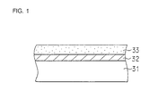
Figure 1 is a cross-sectional view of one embodiment of
a hard carbon film-coated substrate in accordance with a
first aspect of the present invention;
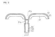
Figure 2 is a cross-sectional view of an electric
shaver embodiment in which the first aspect of the present
invention is applied to inner and outer blades thereof;
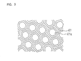
Figure 3 is a plan view showing a planar pattern of an
outer blade of the electric shaver;
Figure 4 is a front view showing an inner blade of the
electric shaver;
Figure 5 is a schematic block diagram of an apparatus
for forming an interlayer and a hard carbon film as employed
in the embodiments in accordance with the first aspect of
the present invention;
Figure 6 is a plan view showing a leading end of a
reaction gas inlet line of the apparatus shown in Figure 5
and its vicinities;
Figure 7 is a schematic cross-sectional view showing a
general construction of a rotary compressor;
Figure 8 is a schematic cross-sectional view of a hard
carbon film-coated vane in accordance with the first aspect
of the present invention;
Figure 9 is a schematic cross-sectional view of a hard
carbon film-coated roller in accordance with the first
aspect of the present invention;
Figure 10 is a schematic cross-sectional view of a hard
carbon film-coated cylinder channel in accordance with the
first aspect of the present invention;
Figure 11 is a cross-sectional view of the electric
shaver outer blade having an outer surface on which the
interlayer is formed;
Figure 12 are cross-sectional views showing a series of
steps of electroforming a substrate in accordance with a
second aspect of the present invention and thereafter
forming an interlayer on the substrate;
Figure 13 are cross-sectional views showing another
series of steps of electroforming a substrate in accordance
with the second aspect of the present invention and
thereafter forming an interlayer on the substrate;
Figure 14 is a partly-sectioned side view showing an
exemplary arrangement of inner blades of an electric shaver
on which respective interlayers are formed by plating in
accordance with the second aspect of the present invention;
and
Figure 15 is a partly-sectioned side view showing a
comparative arrangement of inner blades of an electric
shaver on which respective interlayers are formed by
sputtering.
DESCRIPTION OF THE PREFERRED EMBODIMENTS
Figure 1 is a cross-sectional view of one embodiment of
a hard carbon film-coated substrate in accordance with a
first aspect of the present invention. Referring to Figure
1, formed on a substrate 31 is an interlayer 32 on which a
hard carbon film, i.e. a diamond-like carbon film 33 is
formed. The thickness of the interlayer 32 is preferably in
the range of 50-8000Å, more preferably in the range of 50-4000Å.
The thickness of the diamond-like carbon film 33 is
preferably in the range of 50-5000Å, more preferably in the
range of 50-3000Å.
Figure 2 is a cross-sectional view of an electric
shaver blade embodiment in which the present invention is
applied to its inner and outer blades. Referring to Figure
2, formed on an outer blade substrate 41 is an interlayer 42
on which a hard carbon film, i.e. a diamond-like carbon film
43 is formed. Figure 3 is a plan view showing a planar
pattern of the outer blade substrate 41. As illustrated in
Figure 3, the outer blade substrate 41 has a number of holes
41a for catching beards.
Referring back to Figure 2, an inner blade is arranged
inwardly of the outer blade substrate 41. Formed on a
substrate 51 of the inner blade is an interlayer 52 on which
a hard carbon film, i.e. a diamond-like carbon film 53 is
formed. Figure 4 is a front view of the inner blade
substrate 51. As illustrated in Figure 4, the inner blade
substrate 51 has at its upper end tapered surfaces 51a each
of which shows a downward slope (also refer to Figure 2)
from an upper edge when cross-sectioned. Again referring
back to Figure 2, as the inner blade slides on the outer
blade in directions as indicated by arrows, the beards
caught in the holes 41a are cut.
In this particular embodiment, the outer blade
substrate 41 is formed of Ni whereas the inner blade
substrate 51 is formed of stainless steel (SUS).
Figure 5 is a schematic block diagram of a thin film
formation apparatus within which both of the interlayer and
the hard carbon film can be formed. Referring to Figure 5,
disposed interior of a vacuum chamber 8 is a plasma
generation chamber 4 to which one end of a waveguide 2 is
connected. The waveguide 102 has another end to mount a
microwave supplying means 1. The microwaves generated
within the microwave supplying means 1 pass through the
waveguide 2 and a microwave inlet window 3 to be guided into
the plasma generation chamber 4. Connected to the plasma
generation chamber 4 is a discharge gas inlet line 5 for
introducing a discharge gas such as argon (Ar) into the
plasma generation chamber 4. A plurality of plasma magnetic
field generators 6 are mounted circumferentially of the
plasma generation chamber 4. A high-density plasma can be
produced within the plasma generation chamber 4 by
influencing a high-frequency magnetic field produced by the
microwave upon the magnetic field produced by the plasma
magnetic field generators 6.
A drum-shaped substrate holder 12 is provided within
the vacuum chamber 8 so as to be rotatable about an axis
(not shown) which arranged perpendicularly to a wall surface
of the vacuum chamber 8. A number of substrates 13 is
arranged circumferentially of the substrate holder 12 at
regular intervals. A high-frequency power source 10 is
connected to the substrate holder 12.
A hollow cylindrical shielding cover 14, made of metal,
radially surrounds the substrate holder 12 to define
therebetween a predetermined spacing. The shielding cover
14 is connected to a grounded electrode. The shielding
cover 14 functions to prevent generation of discharges
between the vacuum chamber 8 and the substrate holder 12
excluding target film-forming locations thereon, which
discharges will be otherwise generated when a radio
frequency (also referred to as RF) voltage is applied to the
substrate holder 12 for film-forming. The spacing between
the substrate holder 12 and the shielding cover 14 may be
dimensioned to be smaller than a mean free path of gaseous
molecules. The mean free path of gaseous molecules is equal
to or smaller than the average distance that ions or
electrons accelerated by an electric field can travel
without collisions. Thus, the probability of collisions
between the gaseous molecules and the ions or electrons can
be lowered to thereby prevent the molecules from undergoing
chain electrolytic dissociations by dimensioning the spacing
between the substrate holder 12 and the shielding cover 14
not to exceed the mean free path of the gaseous molecules.
It is preferred that the spacing between the substrate
holder 12 and the shielding cover 14 is dimensioned not to
exceed one tenth of the mean free path of the gaseous
molecules. In this particular embodiment of the apparatus,
the spacing between the substrate holder 12 and the
shielding cover 14 is dimensioned to be about 5 mm so as
not to exceed one tenth of the mean free path of the gaseous
molecules.
The shielding cover 14 has at its top a first opening
15. A plasma from the plasma generation chamber 4 is
directed to pass through the first opening 15 to impact the
substrates 13 mounted on the substrate holder 12. The
vacuum chamber 8 is equipped with a reaction gas inlet line
16. A leading end of the reaction gas inlet line 16 is
positioned above the first opening 15.
Figure 6 is a plan view showing the leading end of the
reaction gas inlet line 16 and its vicinities. Referring to
Figure 6, the reaction gas inlet line 16 includes a gas
inlet portion 16a for introducing a CH4 gas into the vacuum
chamber 8 and a gas discharge portion 16b for perpendicular
connection to the gas inlet portion 16a. The gas discharge
portion 16b is arranged to perpendicularly cross a
rotational direction A of the substrate holder 12 and is
positioned above the first opening 15. In the plan view,
the gas discharge portion 16b is located upstream along the
direction A within the first opening 15. The gas discharge
portion 16b has a plurality of holes 21 which are directed
downwardly each at an angle of about 45 degrees. In this
particular embodiment, eight holes 21 are provided as shown
in Figure 6. These holes 21 are spaced from each other at
distances which become smaller toward each end of the gas
discharge portion 16b. The provision of the holes 117 at
such spacings allows the CH4 gas introduced from the gas
inlet portion 16a to be discharged therefrom with a
substantially uniform distribution along the length of the
gas discharge portion 16b.
Referring to Figure 5, the shield cover 14 has at its
bottom a second opening 17 facing the first opening 15. A
target 18 is disposed below the second opening 17 to
upwardly face the second opening 17. Connected to the
target 18 is an RF power source 19 for sputtering the target
18. The target 18 and the RF power source constitutes a
means for forming the interlayer. Accordingly, in the
apparatus of Figure 5, the hard carbon film is formed by the
plasma CVD method at a location of the first opening 15
while the interlayer is formed by sputtering at a location
of the second opening 17.
The employment of such an apparatus as shown in Figure
5 enables the simultaneous formation of thin films on a
number of substrates.
EXAMPLE 1 (Interlayer: B)
The apparatus of Figure 5 was employed to form the
interlayer and the diamond-like carbon film. A partial
pressure of the Ar gas within the vacuum chamber 8 was set
at 1.5 x 10⁻³ Torr. B was used as the target 18 and a power
supplied to the target 18 was set at 200 W. The interlayer
comprised of B was formed on the Ni substrate 13 by applying
a RF voltage to the substrate holder 12 such that a self-bias
voltage produced in the substrate 13 reached -50 V.
This step was continued for 30 minutes. As a result, the
interlayer was formed to a thickness of about 0.05µm.
Here, twenty four of the Ni substrates 13 were mounted
circumferentially of the substrate holder 12 at regular
intervals. In forming the interlayers on the respective
substrates 13, the substrate holder 12 was rotated at a
speed of about 10 rpm.
A hard carbon film, i.e. a diamond-like carbon film was
then formed on the interlayer overlying the Ni substrate 13.
An interior of the vacuum chamber 8 was controlled at a
pressure of 10-5-10-7 Torr. The Ar gas at 5.7 x 10⁻⁴ torr.
was then supplied from the discharge gas inlet line 5 of the
ECR plasma generator while a 2.45 GHz, 100 W microwave was
supplied from the microwave supplying means 1, so that an Ar
plasma generated within the plasma generation chamber 4
struck a surface of each substrate 13. Simultaneously, a
13.56 MHz RF voltage from the high-frequency power source 10
was applied to the substrate holder 12 in a controlled
fashion so that a self-bias voltage of -50 V was generated
in each of the substrates 13. A CH4 gas at 1.3 x 10⁻³ Torr.
was supplied through the reaction gas inlet line 16. This
step was continued for about 15 minutes to form the diamond-like
carbon film having a thickness of 1000Å on the surface
of each substrate 13.
EXAMPLE 2 (Interlayer: nitride of B)
The apparatus of Figure 5 was employed as similar to
Example 1. The partial pressures of Ar and N2 gases were
set at 1.5 x 10⁻³ Torr. and 5.0 x 10⁻⁴ Torr., respectively. B
was used as the target and a power supplied to the target
was set at 200 W. The interlayer comprised of nitride of B
was thus formed on the Ni substrate 13. Here, a RF voltage
was applied to the substrate holder 12 so that a self-bias
voltage produced in the substrate 13 reached -50 V. This
interlayer formation was continued for 40 minutes. As a
result, the interlayer comprised of BN was formed to a
thickness of about 0.05µm.
Subsequently, the diamond-like carbon film was formed
on the interlayer to a thickness of 1000Å in the same
manner as in Example 1.
EXAMPLE 3 (Interlayer: oxide of Al)
The apparatus of Figure 5 was employed as similar to
Example 1. The partial pressures of Ar and O2 gases were
set at 1.5 x 10⁻³ Torr. and 1.0 x 10⁻³ Torr., respectively.
Al was used as the target and a power supplied to the target
was set at 400 W. The interlayer comprised of oxide of Al
was thus formed on the Ni substrate 13. Here, a RF voltage
was applied to the substrate holder 12 so that a self-bias
voltage of -50 V was produced in the substrate 13. This
interlayer formation was continued for 30 minutes. As a
result, the interlayer was formed to a thickness of about
0.04µm.
Subsequently, the diamond-like carbon film was formed
on the interlayer to a thickness of 1000Å in the same
manner as in Example 1.
EXAMPLE 4 (Interlayer: nitride of Cr)
The apparatus of Figure 5 was employed as similar to
Example 1. The partial pressures of Ar and N2 gases were
set at 1.5 x 10⁻³ Torr. and 1.0 x 10⁻³ Torr., respectively.
Cr was used as the target and a power supplied to the target
was set at 400 W to form the interlayer, comprised of
nitride of Cr, on the Ni substrate 13. Here, a RF voltage
was applied to the substrate holder 12 so that a self-bias
voltage of -50 V was produced in the substrate 13. This
interlayer formation was continued for 30 minutes. As a
result, the interlayer was formed to a thickness of about
0.05µm.
Subsequently, the diamond-like carbon film was formed
on the interlayer to a thickness of 1000Å in the same
manner as in Example 1.
EXAMPLE 5 (Interlayer: oxide of Sn)
The apparatus of Figure 5 was employed as similar to
Example 1. The partial pressures of Ar and O2 gases were
set at 1.5 x 10⁻³ Torr. and 1.0 x 10⁻³ Torr., respectively.
Sn was used as the target and a power supplied to the target
was set at 400 W to form the interlayer, comprised of oxide
of Sn, on the Ni substrate 13. Here, a RF voltage was
applied to the substrate holder 12 so that a self-bias
voltage of -50 V was produced in the substrate 13. This
interlayer formation was continued for 30 minutes. As a
result, the interlayer was formed to a thickness of about
0.04µm.
Subsequently, the diamond-like carbon film was formed
on the interlayer to a thickness of 1000Å in the same
manner as in Example 1.
EXAMPLE 6 (Interlayer: Co)
The apparatus of Figure 5 was employed as similar to
Example 1. The partial pressure of Ar was set at 1.5 x 10⁻³
Torr. Co was used as the target and a power supplied to the
target was set at 400 W to form the interlayer, comprised of
Co, on the Ni substrate 13. Here, a RF voltage was applied
to the substrate holder 12 so that a self-bias voltage of -
50 V was produced in the substrate 13. This interlayer
formation was continued for 30 minutes. As a result, the
interlayer was formed to a thickness of about 0.05µm.
Subsequently, the diamond-like carbon film was formed
on the interlayer to a thickness of 1000Å in the same
manner as in Example 1.
COMPARATIVE EXAMPLE 1
For comparative purposes, a diamond-like carbon film
was directly formed on a Ni substrate without intervention
of an interlayer therebetween. The diamond-like carbon film
formation was performed in the same conditions as used in
Example 1.
The diamond-like carbon film-coated Ni substrates as
obtained in Examples 1-6 and Comparative Example 1 were
evaluated for their levels of adhesion. The adhesion
evaluation was made by an indentation test in which a
Vickers indenter was forced under a constant load (Load = 1
kg) into surfaces of the substrates. Fifty samples were
taken for each diamond-like carbon film-coated Ni substrate,
and the number of samples which showed delamination of the
diamond-like carbon film from the Ni substrate was counted
as being indicative of a level of adhesion of the hard
carbon film. Results are given in Table 1.
| | Example No. | Comp. Example No. |
| | 1 | 2 | 3 | 4 | 5 | 6 | 1 |
| Number of Samples | 0 | 0 | 0 | 0 | 0 | 0 | 43 |
As apparent from the results given in Table 1, each of
the diamond-like carbon film-coated Ni substrates of
Examples 1-6, which incorporated the interlayer in
accordance with the first aspect of the invention, shows the
number of its samples that experienced delamination as being
much smaller relative the diamond-like carbon film-coated Ni
substrate of Comparative Example 1. This demonstrates that
the provision of the interlayer in accordance with the first
aspect of the present invention enhances the adhesion of the
diamond-like carbon film to the Ni substrate.
Figure 7 is a schematic cross-sectional view showing a
general construction of a rotary compressor.
Referring to Figure 7, the rotary compressor includes a
closed container 101, a crank shaft 102 driven by an
electric motor (not shown), and a roller 103 mounted
eccentric to the crank shaft 102. The roller 103 is made of
Mo-Ni-Cr cast iron.
A hollow cylinder 104 of cast iron is disposed to
accommodate the roller 103 therein.
The hollow cylinder 104 has a cylinder channel 105
within which a vane 106 reciprocates. The vane 106
partitions a space interior of the hollow cylinder 104 into
a high-pressure part and a low-pressure part. The vane 106
is made of high-speed tool steel (SKH51).
The vane 106 is urged against the roller 103 by a
spring 107.
An inlet tube 108 is provided to supply a refrigerant
carrier into the interior of the hollow cylinder 104. The
refrigerant carrier pressurized and heated within the hollow
cylinder 104 is exhausted through an exhaust tube 109 to the
exterior of the compressor.
The operation of the rotary compressor as constructed
in the manner as described above will be now explained.
When the electric motor drives the crank shaft 102, the
roller 103 mounted eccentric to the crank shaft 102 moves
circumferentially along an inner surface of the hollow
cylinder 104 while rotating. Since the vane 106 is urged
against the roller 103 by both a pressurized gas and the
spring 107, the vane 106 is brought into a constant contact
with a periphery of the roller 3. Accordingly, a rotational
motion of the roller 103 is translated into a reciprocating
motion of the vane 106 within the cylinder channel 105.
As such a reciprocating motion is continued, the
refrigerant carrier is suctioned through the inlet tube 108
into the interior of the hollow cylinder 104 within which
the refrigerant carrier is compressed to increase its
temperature and pressure before it is discharged through the
exhaust tube 109 to the exterior of the rotary compressor.
Figure 8 is a schematic cross-sectional view of the
vane 106 carrying a hard carbon coating film thereon, in
accordance with the first aspect of the present invention.
Formed on the vane 106 is an interlayer 161 on which a hard
carbon film 162 is formed.
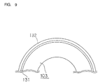
Figure 9 is a schematic cross-sectional view of the
roller 103 carrying thereon a hard carbon film, in
accordance with the first aspect of the present invention.
Formed on the roller 103 is an interlayer 131 on which a
hard carbon film 132 is formed.
Figure 10 is a schematic cross-sectional view of the
cylinder channel 105 carrying thereon a hard carbon film, in
accordance with the first aspect of the present invention.
Formed on an inner surface of the cylinder channel 105 is an
interlayer 151 on which a hard carbon film 152 is formed.
The hard carbon film provided on the vane 106 of Figure
8 was then tested for evaluating its adhesion level. The
apparatus of Figure 5 was employed. The partial pressure of
Ar gas was set at 1.5 x 10⁻³ Torr. Cr was used as a target
and a power supplied to the target was set at 400 W to form
a Cr interlayer on the vane 106. Here, a RF voltage was
applied to the substrate holder so that a self-bias voltage
of -50 V was produced in the substrate. This interlayer
formation was continued for 30 minutes. As a result, the
interlayer was formed to a thickness of about 0.05µm.
Subsequently, the hard carbon film formation was
continued for 75 minutes in the same manner as in Example 1
so that the hard carbon film 162 was formed on the
interlayer 161 to a thickness of about 5000Å.
The hard carbon film-coated substrate thus obtained was
tested for evaluating its level of adhesion. The adhesion
evaluation was made by an indentation test in which a
diamond-sphere indenter having a tip radius of 0.1 mm was
forced under a constant load (Load = 500 g) into a surface
of the substrate. Fifty samples were taken for the hard
carbon film-coated
vane 106, and the number of samples which
showed delamination of the
hard carbon film 162 from the
vane 106 was counted as being indicative of a level of
adhesion of the hard carbon film. For comparative purposes,
a hard carbon film was directly formed on the
vane 106,
without intervention of the Cr interlayer, by applying a RF
voltage to the substrate holder such that a self-bias
voltage of -50 V was produced in the
vane 106. The obtained
hard carbon film was also tested for evaluating its adhesion
to the vane. Results are given in Table 2.
| Cr Interlayer | Self-Bias Voltage (V) | Number of Samples |
| Absent | -50 | 45 |
| Present | -50 | 5 |
As can be clearly seen from Table 2, in the case where
the Cr interlayer 161 was absent on the vane 106, forty five
samples showed delamination of the hard carbon film 162 even
if the self-bias voltage of -50 V was produced in the vane.
In contrast, in the case where the Cr interlayer 161 was
present on the vane 106 and the hard carbon film 162 was
formed on the interlayer 161 at the self-bias voltage of -50
V, only five samples showed delamination of the hard carbon
film 162.
In the above Examples, the interlayer was specified to
be formed by sputtering. However, the method of forming the
interlayer in accordance with the first aspect of the
present invention is not limited to sputtering. The
interlayer can be formed by the other methods including the
other physical thin film formation methods such as
deposition methods, chemical vapor phase epitaxial methods
such as CVD methods, and plating methods. Although the
apparatus of Figure 5 was employed in the above Examples to
form both the interlayer and the hard carbon film, the other
apparatuses may be employed to separately form the
interlayer and the hard carbon film.
The provision of the interlayer between the substrate
and the hard carbon film, in accordance with the first
aspect of the present invention, enhances adhesion and peel
resistance of the hard carbon film.
The preferred embodiments in accordance with the second
aspect of the present invention will be now described.
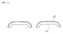
Figure 11 is a cross-sectional view of an outer blade
substrate 41 on which an interlayer 42 is formed by plating.
The outer blade substrate may be electroformed, for example.
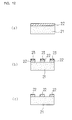
Figure 12 are cross-sectional views showing the steps
of forming the interlayer by plating, subsequent to
electroforming the outer blade substrate. As shown in
Figure 12(a), a metallic layer 22 is provided on a plastic
plate 21 by plating nickel or applying a copper foil on the
plastic plate 21. The metallic layer 23 is coated with a
resist 23 in such a pattern as corresponding to an outer
blade of an electric shaver. The resist 23 protects the
coated area of the metallic layer 23 from the action of an
etchant so that the metallic layer 23 is etched to the
predetermined pattern of the outer blade for an electric
shaver, as shown in Figure 12(b). The subsequent removal of
the resist 23 leaves the metallic layer 22 having the
pattern of the electric shaver outer blade on the plastic
plate 21, as shown in Figure 12(c).
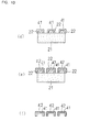
As shown in Figure 13(d), a nickel plating is applied
to the metallic layer 22 to obtain the outer blade substrate
41 for the electric shaver by electroforming. A commonly-employed
electroplating bath may be utilized for the
electroforming. An exemplary electroplating bath contains
30 g/l of nickel chloride, 300 g/l of nickel sulfamate, 30
g/l of boric acid, and a suitable amount of a pit inhibitor.
The electroplating may be carried out in the pH range of
3.5-4.0, at temperatures of 30-60 °C and current densities
of 2-15 A/dm2, for example, to deposit a nickel layer. The
thickness of the nickel layer to be deposited is not
particularly specified, but is generally in the range of 10-100
µm.
The interlayer 42 is subsequently formed on the outer
blade substrate 41 such as by electroplating or electroless
plating while the outer blade substrate 41 is held on the
metallic layer 22, as shown in Figure 13(e). The suitable
plating bath and conditions may be selected depending upon
the type of the interlayer 42 to be deposited by plating.
The thickness of the interlayer 42 generally ranges from
about 50 to 5000 Å.
When the outer blade substrate 41 is removed from the
metallic layer 22, the outer blade substrate 41 for an
electric shaver is obtained which carries the interlayer 42
thereon, as shown in Figure 13(f). A diamond-like or hard
carbon film is then formed on the interlayer to obtain an
electric shaver outer blade having the interlayer through
which the hard carbon film is provided on the outer blade
substrate. Here, the hard carbon film may be formed on the
interlayer 42 after the outer blade substrate 41 carrying
the interlayer 42 has been removed from the metallic layer
22. Alternatively, the hard carbon film may be formed on
the interlayer 42 while the outer blade substrate 41
carrying the interlayer 42 is held on the metallic layer 22.
This follows that the outer blade substrate 41 is removed
from the metallic layer 22 subsequent to the hard carbon
film formation.
EXAMPLE 7
The steps shown in Figures 12 and 13 were taken to
electroform a Ni substrate for an electric shaver outer
blade on which an interlayer of Ru was formed.
A Ni plating bath used in electroforming the Ni
substrate contained 30 g/l of nickel chloride, 300 g/l of
nickel sulfamate, 30 g/l of boric acid, and a suitable
amount of a pit inhibitor. The Ni plating bath was adjusted
to a pH of 3.5 and controlled at a temperature of 50 °C.
The electroforming was then initiated at a current density
of 10 A/dm2 to deposit the Ni substrate on a mold. The
thickness of the Ni substrate was about 50 µm.
The Ru plating was carried out while the Ni substrate
was held on the mold to form the Ru interlayer on the Ni
substrate. An Ru plating bath as employed contained 3 g/l
of ruthenium sulfate, 6 g/l of sulfuric acid and a suitable
amount of additives. The Ru plating bath was adjusted to a
pH of about 1.5 and controlled at a temperature of about 50
°C. The Ru electroplating was then performed at a current
density of 2 A/dm2 to deposit the Ru interlayer on the Ni
substrate. The thickness of the Ru interlayer was about 100
Å.
Subsequent to forming the Ru interlayer on the Ni
substrate as described above, a diamond-like carbon film was
formed on the Ru interlayer using the ECR plasma CVD
apparatus. The partial pressures of the Ar and CH4 gases
were set at 5.7 x 10⁻⁴ Torr. and 1.3 x 10⁻³ Torr.,
respectively. A microwave power of 100 W at a microwave
frequency of 2.45 GHz was supplied during the thin film
formation. The 13.56 MHz RF power from the high-frequency
power source was supplied to the substrate holder in a
controlled fashion so that a self-bias voltage of -50 V was
produced in each of the substrates. The thin film formation
was continued for 15 minutes. As a result, the diamond-like
carbon film was formed to a thickness of 1000 Å.
Thereafter, the Ni substrate was removed from the mold.
EXAMPLE 8
Subsequent to forming the Ni substrate on the mold in
the same manner as in Example 7, a Sn plating was performed
to form a Sn interlayer on the Ni substrate. The employed
Sn plating bath contained 90 g/l of sodium stannate, 8 g/l
of sodium hydroxide and 10 g/l of sodium acetate. The Sn
plating bath was controlled at a temperature of 70 °C. The
Sn electroplating was then performed at a current density of
1.5 A/dm2 to deposit the Sn interlayer on the Ni substrate.
The thickness of the Sn interlayer was about 100 Å.
Subsequent to forming the Sn interlayer, a diamond-like
carbon film was formed on the Sn interlayer in the same
manner as in Example 7 to a thickness of about 1000 Å.
EXAMPLE 9
The Ni substrate was formed on the mold in the same
manner as employed in Example 7. Thereafter, a composite
plating bath which dispersed SiC particles in the Sn plating
bath was used to form the interlayer. The Sn plating bath
was identical to that of Example 8. The SiC particles
having an average particle size of about 0.1 µm were
dispersed in the Sn plating bath to prepare the composite
plating bath containing 10 weight % of the SiC particles.
The plating conditions identical to those of Example 8 were
used to form the interlayer having a thickness of about 0.5
µm and comprised of a Sn film in which the SiC particles
were dispersed. This Sn film contained 5 volume % of the
SiC particles.
Subsequently, a diamond-like carbon film was formed on
the interlayer as similarly to Example 7.
COMPARATIVE EXAMPLE 2
Subsequent to forming the Ni substrate on the mold in
the same manner as in Example 7, a diamond-like carbon film
was directly formed on the Ni substrate without intervention
of any interlayer therebetween. The diamond-like carbon
film formation was performed in the same manner as in
Example 7.
The diamond-like carbon films as respectively obtained
in Examples 7-9 and Comparative Example 2 were evaluated for
their levels of adhesion. The adhesion evaluation was made
by an indentation test in which a Vickers indenter was
forced under a constant load (Load = 1 kg) into surfaces of
the diamond-like carbon films. Fifty samples were taken for
each of the diamond-like carbon films, and the number of
samples which showed delamination of the diamond-like carbon
film from the Ni substrate was counted as being indicative
of a level of adhesion of the diamond-like carbon film.
Results are given in Table 3.
| | Example No. | Comp. Example No. |
| | 7 | 8 | 9 | 2 |
| Number of Samples | 0 | 0 | 0 | 43 |
As can be clearly seen from Table 3, the diamond-like
carbon films of Examples 7-9 each provided on the Ni
substrate through the interlayer exhibit superior peel
resistances relative to the diamond-like carbon film of
Comparative Example 2 to thereby demonstrate a higher level
of adhesion to the Ni substrate.
EXAMPLE 10
The Ru electroplating was performed to form an Ru
interlayer on a substrate for an electric shaver inner blade
as shown in Figure 2. During the Ru electroplating, the
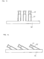
inner blade substrates 51 were held upright on a jig 54 for
coating treatment as shown in Figure 14. The Ru plating
bath and plating conditions as used here were identical to
those of Example 7.
The uniform coverage of the Ru interlayer even on edge
portions of the substrate 51 were recognized.
COMPARATIVE EXAMPLE 3
A sputtering method was used to form an Ru interlayer
52 on the inner blade substrates 51 which were held upright
relative to the jig 54 as shown in Figure 14. The partial
pressure of Ar gas was set at 1.5 x 10⁻³ Torr. Cr was used
as a target and a power supplied to the target was set at
400 W to form the Ru interlayers having a thickness of about
100 Å. The resulting Ru interlayers were observed as
providing poor coverages on respective substrates,
particularly at edge portions of the substrates.
COMPARATIVE EXAMPLE 4
The inner blade substrates 51 were mounted in an
inclined manner to the jig 54 for coating treatment. While
such an arrangement was kept, the Ru interlayer 52 was
formed on each substrate 51 by the sputtering method as
analogously to Comparative Example 3. The inner blade
substrates 51 were then rearranged to incline in the
opposite direction prior to supplemental interlayer
formation thereon. As a result, the interlayer coating was
improved at edge porions of the substrate to provide the
substantially uniform interlayer around the substrate.
As can be appreciated by comparing Example 10 with
Comparative Examples 3 and 4, the interlayer formation by
plating, in accordance with the second aspect of the present
invention, is effective in providing a uniform thin film
coating even on a substrate having complicated three-dimensional
configurations. Thus, the formation of a hard
carbon film on such an interlayer can improve adhesion of
the hard carbon film to the substrate.
In the above Examples, the interlayer was formed on the
inner and outer blade substrates for an electric shaver for
subsequent hard carbon film formation thereon. However,
those inner and outer blade substrates serve as exemplary
purposes only, and should not be considered as limiting. It
should be understood that the present invention is
applicable to other types of substrates. Although the
interlayer is also described in the above Examples to be
formed by electroplating, the interlayer may be formed by
electroless plating in the present invention.
It should be also understood that the second aspect of
the present invention can be applied only one of the inner
and outer electric shaver blades. Although the interlayer
and the hard carbon film are described in the above Examples
to be formed only on the outer surface of the electric
shaver outer blade, they may be additionally formed on the
inner surface of the electric shaver outer blade.
In accordance with the second aspect of the present
invention, the interlayer is formed on the substrate by
plating. This enables a uniform formation of the interlayer
even on the substrate having complicated three-dimensional
configurations, such as electric shaver outer and inner
blades, and provides an improved adhesion of the hard carbon
film formed on the interlayer to the substrate.
Also, in accordance with the second aspect of the
present invention, the electroforming method is utilized to
deposit the substrate on the mold, and thereafter the
interlayer is formed on the substrate by plating.
Accordingly, it is possible to form the interlayer while the
substrate is held on the mold, consecutive to the substrate
formation. This simplifies the fabricating steps to
increase the production efficiency of the hard carbon film-coated
substrate.