EP1067462A1 - A computer peripheral apparatus and a computer readable medium having a program for controlling the computer peripheral apparatus - Google Patents
A computer peripheral apparatus and a computer readable medium having a program for controlling the computer peripheral apparatus Download PDFInfo
- Publication number
- EP1067462A1 EP1067462A1 EP00114066A EP00114066A EP1067462A1 EP 1067462 A1 EP1067462 A1 EP 1067462A1 EP 00114066 A EP00114066 A EP 00114066A EP 00114066 A EP00114066 A EP 00114066A EP 1067462 A1 EP1067462 A1 EP 1067462A1
- Authority
- EP
- European Patent Office
- Prior art keywords
- central processing
- processing unit
- controllers
- computer
- memory space
- Prior art date
- Legal status (The legal status is an assumption and is not a legal conclusion. Google has not performed a legal analysis and makes no representation as to the accuracy of the status listed.)
- Granted
Links
Images


Classifications
-
- H—ELECTRICITY
- H04—ELECTRIC COMMUNICATION TECHNIQUE
- H04L—TRANSMISSION OF DIGITAL INFORMATION, e.g. TELEGRAPHIC COMMUNICATION
- H04L12/00—Data switching networks
- H04L12/28—Data switching networks characterised by path configuration, e.g. LAN [Local Area Networks] or WAN [Wide Area Networks]
- H04L12/40—Bus networks
- H04L12/40052—High-speed IEEE 1394 serial bus
- H04L12/40123—Interconnection of computers and peripherals
-
- G—PHYSICS
- G06—COMPUTING; CALCULATING OR COUNTING
- G06F—ELECTRIC DIGITAL DATA PROCESSING
- G06F13/00—Interconnection of, or transfer of information or other signals between, memories, input/output devices or central processing units
- G06F13/38—Information transfer, e.g. on bus
- G06F13/382—Information transfer, e.g. on bus using universal interface adapter
- G06F13/385—Information transfer, e.g. on bus using universal interface adapter for adaptation of a particular data processing system to different peripheral devices
Definitions
- the present invention relates to a computer peripheral apparatus having both a central processing unit (hereafter, the "central processing unit” will be referred to as the "CPU") which is operated on the basis of firmware stored in a nonvolatile memory and, an interface which can be connected to a computer. More particularly, the present invention relates to a computer peripheral apparatus in which mutually different interfaces can be mounted, and relates to a computer readable medium having a program for controlling the computer peripheral apparatus.
- CPU central processing unit
- a scanner, a printer, and the like are known as peripheral apparatuses which can be connected to a computer and have CPUs.
- firmware for operating the CPU is generally stored in a nonvolatile memory.
- interfaces for connecting a computer and its peripheral apparatuses have come to be diversified.
- a scanner can be connected to the computer by a SCSI, a USB, IEEE 1394, and the like.
- EPROMs storing firmware need to be prepared in a number corresponding to the number of types of interfaces, and different EPROMs need to be mounted for the respective types having different interfaces.
- firmware of the peripheral apparatus has come to be stored in a flash memory which is rewritable in the state of being mounted on a board.
- firmware which is different for each interface is stored in the flash memory, it is also necessary to prepare firmware in a number corresponding to the number of types of interfaces, and write the firmware in correspondence with the types of interfaces. For this reason, with conventional peripheral apparatuses, there has been a problem in that the development of firmware for each interface and management of supply thereof become complicated.
- the present invention has been devised to overcome the above-described problem, and its object is to provide a computer peripheral apparatus which can be operated by the same firmware even if the interface is different.
- a computer peripheral apparatus comprising a central processing unit, a plurality of interface units of different types including controllers which control data transfer between a computer and the central processing unit, a plurality of controlling means, one of which mutually transfers signals between the central processing unit and one of the plurality of interface units, and identifying means which identifies a type of one of the controllers, and which operates the central processing unit by using one of the plurality of controlling means that corresponds to the one of the controllers.
- firmware including a plurality of modules corresponding to the plurality of controlling means and a module corresponding to the identifying means is stored in a nonvolatile memory, it is unnecessary to replace the nonvolatile memory in correspondence with the interface unit.
- the computer peripheral apparatus having the same function but having a different interface unit can be operated by the same firmware, the development of firmware and management of supply thereof are facilitated.
- the identifying means writes a value in a predetermined region of memory space of the central processing unit, and identifies the type of one of the controllers by a return value which is obtained by reading data from the predetermined region of the memory space of the central processing unit.
- the controlling means can be selected in accordance with the type of the interface unit by making use of the fact that the assignment of controllers in the memory space, the numbers of registers, or the attributes of the registers differ in the interface units of different types, so as to operate the central processing unit.
- the controllers of the plurality of interface units are assigned to respective regions in the memory space of the central processing unit which are mutually different. Accordingly, even if the numbers, attributes, and the like of the registers in the interface units of different types are the same, the controlling means can be selected in accordance with the type of the interface unit, so as to operate the central processing unit.
- the plurality of interface units have registers in the respective controllers, and wherein numbers of the registers are mutually different. Accordingly, even if the assignments of controllers in the memory space are identical in the interface units of different types, the computer peripheral apparatus is able to select the controlling means in accordance with the type of the interface unit, so as to operate the central processing unit.
- the plurality of interface units have registers in the respective controllers, and wherein attributes of the registers are mutually different. Accordingly, even if the assignments of controllers in the memory space are identical in the interface units of different types, and even if the numbers of the registers are identical, the computer peripheral apparatus is able to select the controlling means in accordance with the type of the interface unit, so as to operate the central processing unit.
- the plurality of interface units receive different inputs thereto from the central processing unit. Accordingly, even if the numbers and attributes of the registers, assignments of memory space, and the like for the interface units of different types are the same, the controlling means can be selected in accordance with the type of the interface unit, so as to operate the central processing unit.
- a computer readable medium having a program stored thereon for controlling a computer peripheral apparatus which includes a central processing unit and a plurality of interface units of different types including controllers which control data transfer between a computer and the central processing unit.
- the program comprises the steps of mutually transferring signals between the central processing unit and one of the plurality of interface units, identifying a type of one of the controllers, and operating the central processing unit in accordance with the type of one of the controllers identified in the identifying step.
- firmware including a plurality of modules for mutually transferring signals between the central processing unit and one of the plurality of interface units and a module for identifying a type of one of the controllers and operating the central processing unit in accordance with the type of one of the controllers is stored in a nonvolatile memory through a computer readable medium, it is unnecessary to replace the firmware in correspondence with the interface unit.
- the computer peripheral apparatus having the same function but having a different interface unit can be operated by the same firmware, the development of firmware and management of supply thereof are facilitated.
- the identifying step comprising writing a value in a predetermined region of memory space of the central processing unit; and identifying the type of one of the controllers by a return value which is obtained by reading data from the predetermined region of the memory space of the central processing unit.
- the controlling procedure can be selected in accordance with the type of the interface unit by making use of the fact that the assignment of controllers in the memory space, the numbers of registers, or the attributes of the registers differ in the interface units of different types, so as to operate the central processing unit.
- the above-described program may be stored in the computer through a communication means, and the program can be written in the computer peripheral apparatus by the computer.
- the computer readable medium of the seventh aspect of the present invention may be considered in combination with the computer peripheral apparatus of the first aspect of the present invention. That is, there may be provided a computer readable medium having a program stored thereon for controlling a computer peripheral apparatus which includes a central processing unit, a plurality of interface units of different types including controllers which control data transfer between a computer and the central processing unit, a plurality of controlling means, and identifying means, wherein the program causes one of the plurality of controlling means to mutually transfer a signal between the central processing unit and one of the plurality of interface units, and wherein the program causes the identifying means to identify a type of one of the controllers and operate the central processing unit by using one of the plurality of controlling means that corresponds to the one of the controllers.
- the program causes the identifying means to write a value in a predetermined region of memory space of the central processing unit and identify the type of one of the controllers by a return value which is obtained by reading data from the predetermined region of the memory space of the central processing unit.
- a data signal tor storing the above-described program in the computer.
- FIG. 2 shows a configuration of hardware in accordance with a first embodiment to which the present invention is applied to a scanner.
- a scanner 1 is a computer peripheral apparatus which transmits image data to a computer 2 by using an unillustrated CCD.
- the scanner 1 has a CPU 11, a reading unit 12, a read only memory (ROM) 13, a random access memory (RAM) 14, and an interface unit 15.
- the CPU 11, the reading unit 12, the read only memory (ROM) 13, the random access memory (RAM) 14, and the interface unit 15 are stored in an unillustrated casing.
- An external connection port 15b of the interface unit 15 is exposed on the outer side of the casing, and is connected to the computer 2 by a cable 16.
- the reading unit 12 has an unillustrated reciprocatable carriage, and outputs the brightness of each pixel of an original as image data by the CCD stored in the carriage.
- the CPU 11 is connected to a controller of such as the reading unit 12 through an unillustrated chip select, and controls the overall scanner 1.
- the RAM 14 temporarily stores the image data outputted from the reading unit 12.
- the ROM 13 which is a nonvolatile memory is a UV-EPROM, and firmware for operating the CPU 11 is stored therein.
- the nonvolatile memory may be a flash memory.
- the flash memory is used as the nonvolatile memory
- firmware is provided by a computer readable medium such as a floppy disk
- the downloading of firmware becomes possible through a communication line by using a communication means such as the Internet.
- the interface unit 15 has a controller 15a for controlling the transfer of data between the computer 2 and the CPU 11, as well as the external connection port 15b.
- the CPU 11 controls the controller 15a of the interface unit 15 in accordance with a memory-mapped I/O system.
- Two kinds of interface units are prepared as interface units which can be mounted in the scanner 1.
- One is a SCSI-compatible interface unit having a SCSI port, and the other is an IEEE 1394-compatible interface unit having an IEEE 1394 port.
- the controller of the SCSI-compatible interface unit and the controller of the IEEE 1394-compatible interface unit have mutually different assigned regions in memory space. Namely, the chip selects of the CPU 11 to which the respective controllers are assigned are different. A description has been given above of the configuration of hardware in accordance with the first embodiment.
- Fig. 3 shows the configuration of software of the firmware.
- Firmware 20 includes a main module 21, an identifying module 22, and interface modules 23 and 24.
- the main module 21 is a module which is not dependent on the interface unit 15, and is a module for operating the CPU 11 to control the overall scanner 1.
- the identifying module 22 serving as an identifying means is a module which writes a value in a predetermined region of the memory space during the starting of the scanner 1, identifies the type of the interface unit 15 by its return value, and selects either the interface module 23 or 24 depending on the type of the interface unit 15, so as to operate the CPU 11.
- the interface modules 23 and 24 serving as controlling means are modules which operate the CPU 11 depending on the type of the interface unit 15 and mainly cause the CPU 11 to issue a command to the controller 15a.
- the interface module 23 controls the SCSI-compatible interface unit, while the interface module 24 controls the IEEE 1394-compatible interface unit.
- the CPU 11 When the scanner 1 is started, the CPU 11 writes data in a predetermined region of the memory space by means of the identifying module 22. When the region where the data is written by the CPU 11 and the region of the memory space assigned to an I/O register of the controller 15a coincide with each other, if the CPU 11 reads out the data from that region, a valid return value is acquired. Meanwhile, when the region where the data is written by the CPU 11 and the region of the memory space assigned to the I/O register of the controller 15a do not coincide with each other, if the CPU 11 reads out the data from that region, an invalid return value is acquired.
- an assigned region in the memory space of a controller 40a of a SCSI-compatible interface unit 40 having a SCSI port 40b is a region having addresses 10000 through 10004, while an assigned region in the memory space of a controller 41a of an IEEE 1394-compatible interface unit 41 having an IEEE 1394 port 41b is a region having addresses 20000 through 20004. Further, it is assumed that a region in the memory space where the CPU 11 writes data by means of the identifying module 22 is always a region having an address 10000.
- the identifying module 22 operates the CPU 11 on the basis of either module corresponding to the type of the interface unit 15 between the interface modules 23 and 24. For this reason, a signal is transmitted from the CPU 11 to the controller 15a in accordance with the type of the interface unit 15, and a signal transmitted from the controller 15a is processed by the CPU 11.
- the scanner 1 in accordance with the first embodiment of the present invention, it is possible to operate the CPU 11 of the scanner in which the SCSI-compatible interface unit or the IEEE 1394-compatible interface unit is mounted by using single firmware. For this reason, it is unnecessary to replace the ROM 13 in accordance with the type of the interface unit. Therefore, it is unnecessary to manage the firmware for each type of the interface unit.
- the interface modules 23 and 24 have sufficiently small data sizes as compared with the main module 21, the amount of memory space consumed by recording a plurality of interface modules in the ROM 13 is very small.
- the SCSI-compatible interface unit and the IEEE 1394-compatible interface unit have the same chip select for connection to the CPU 11. Namely, their assigned regions in the memory space are identical. Meanwhile, the SCSI-compatible interface unit and the IEEE 1394-compatible interface unit have different numbers of I/O registers of their respective controllers.
- the identifying module is a module which writes a value in the memory space assigned to the I/O register of the controller 15a during the starting of the scanner, identities the type of the interface unit 15 by its return value, and selects either the interface module 23 or 24 depending on the type of the interface unit 15, so as to operate the CPU 11.
- the CPU 11 When the scanner is started, the CPU 11 writes data at a predetermined address in the region assigned to the controller 15a in the memory space by means of the identifying module.
- an I/O register of the controller 15a When an I/O register of the controller 15a has been assigned to the region where the data is written by the CPU 11, if the CPU 11 reads out the data from that region, a valid return value is acquired. Meanwhile, when the I/O register of the controller 15a has not been assigned to the region where the data is written by the CPU 11, if the CPU 11 reads out the data from that region, an invalid return value is acquired.
- Figs. 4A and 4B five registers 32 provided in a controller 42a of a SCSI-compatible interface unit 42 having a SCSI port 42b is assigned to addresses 10000 through 10004 in the memory space, while seven registers 33 provided in a controller 43a of an IEEE 1394-compatible interface unit 43 having an IEEE 1394 port 43b is assigned to addresses 20000 through 20004. Further, it is assumed that the CPU 11 writes data in a region having an address 10005 in the memory space by means of the identifying module.
- the CPU 11 identifies the type of the interface unit mounted in the scanner by means of its return value.
- the identifying module is able to identify the types of the interface units. For this reason, it is unnecessary to assign a plurality of chip selects of the CPU 11 to the controllers of the interface units. Accordingly, the number of controllers other than the interface unit 15 controlled by the CPU 11 can be increased, as required.
- the SCSI-compatible interface unit and the IEEE 1394-compatible interface unit have the same chip select for connection to the CPU 11. Namely, their assigned regions in the memory space are identical.
- the SCSI-compatible interface unit and the IEEE 1394-compatible interface unit have the same numbers of registers of their respective controllers. Meanwhile, the attributes of the registers differ from each other.
- the identifying module is a module which writes a value in the memory space assigned to the I/O register of the controller 15a during the starting of the scanner, identifies the type of the interface unit 15 by its return value, and selects either the interface module 23 or 24 depending on the type of the interface unit 15, so as to operate the CPU 11.
- the CPU 11 When the scanner is started, the CPU 11 writes data at a predetermined address in the region assigned to the I/O register of the controller 15a in the memory space by means of the identifying module. A return value which differs from the written data is acquired depending on the attribute of the register into which the data is written by the CPU 11.
- five registers 34 provided in a controller 44a of a SCSI-compatible interface unit 44 having a SCSI port 44b and five registers 35 provided in a controller 45a of an IEEE 1394-compatible interface unit 45 having an IEEE 1394 port 45b both have 8-bit register lengths, and that the registers 34 and 35 are respectively assigned to addresses 10000 to 10004 in the memory space.
- the first two bits of each register 34 are exclusively used for reading, and are always adapted to return values of zeros.
- the first four bits of each register 35 are exclusively used for reading, and are always adapted to return values of zeros.
- the CPU 11 identifies the type of the interface unit 15 mounted in the scanner by means of its return value.
- the accessing method for the CPU 11 and the I/O register may be based on word accessing in one interface unit so as to change the attributes of the registers.
- the identifying module is able to identify the types of the interface units. For this reason, it is unnecessary to assign a plurality of chip selects of the CPU 11 to the controllers of the interface units. Accordingly, the number of controllers other than the interface unit 15 controlled by the CPU 11 can be increased. Further, even if the numbers of I/O registers of the interface units of different types are identical, the identifying module is able to identify the type of the interface unit.
- the SCSI-compatible interface unit and the IEEE 1394-compatible interface unit have the same chip select for connection to the CPU 11. Namely, their assigned regions in the memory space are identical. In addition, as for the SCSI-compatible interface unit and the IEEE 1394-compatible interface unit, both the numbers and attributes of the I/O registers of their controllers are the same. Meanwhile, inputs to the interface unit 15 of the CPU 11 differ.
- the input to the terminal of an I/O port Pxx is set to high level for the SCSI-compatible interface unit, while the input to the terminal of an I/O port Pxx is set to low level for the IEEE 1394-compatible interface unit. If the input to the interface unit 15 of the CPU 11 is thus made different between the SCSI-compatible interface unit and the IEEE 1394-compatible interface unit, the return values at the time when the identifying module is executed differ. Accordingly, it is possible to identify the type of the interface unit 15 mounted in the scanner by means of its return value.
- the present invention is also applicable to other computer peripheral apparatuses such as a printer.
Abstract
Description
- The present invention relates to a computer peripheral apparatus having both a central processing unit (hereafter, the "central processing unit" will be referred to as the "CPU") which is operated on the basis of firmware stored in a nonvolatile memory and, an interface which can be connected to a computer. More particularly, the present invention relates to a computer peripheral apparatus in which mutually different interfaces can be mounted, and relates to a computer readable medium having a program for controlling the computer peripheral apparatus.
- The present application is based on Japanese Patent Application No. Hei. 11-191635, which is incorporated herein by reference.
- A scanner, a printer, and the like are known as peripheral apparatuses which can be connected to a computer and have CPUs. In such a peripheral apparatus, firmware for operating the CPU is generally stored in a nonvolatile memory. In addition, in recent years, interfaces for connecting a computer and its peripheral apparatuses have come to be diversified. For example, a scanner can be connected to the computer by a SCSI, a USB, IEEE 1394, and the like.
- However, in a conventional peripheral apparatus having an erasable programmable read only memory (EPROM) as a nonvolatile memory, EPROMs storing firmware need to be prepared in a number corresponding to the number of types of interfaces, and different EPROMs need to be mounted for the respective types having different interfaces. Further, in recent years, firmware of the peripheral apparatus has come to be stored in a flash memory which is rewritable in the state of being mounted on a board. In a case where firmware which is different for each interface is stored in the flash memory, it is also necessary to prepare firmware in a number corresponding to the number of types of interfaces, and write the firmware in correspondence with the types of interfaces. For this reason, with conventional peripheral apparatuses, there has been a problem in that the development of firmware for each interface and management of supply thereof become complicated.
- The present invention has been devised to overcome the above-described problem, and its object is to provide a computer peripheral apparatus which can be operated by the same firmware even if the interface is different.
- According to the first aspect of the present invention, there is provided a computer peripheral apparatus comprising a central processing unit, a plurality of interface units of different types including controllers which control data transfer between a computer and the central processing unit, a plurality of controlling means, one of which mutually transfers signals between the central processing unit and one of the plurality of interface units, and identifying means which identifies a type of one of the controllers, and which operates the central processing unit by using one of the plurality of controlling means that corresponds to the one of the controllers. For example, in a case where firmware including a plurality of modules corresponding to the plurality of controlling means and a module corresponding to the identifying means is stored in a nonvolatile memory, it is unnecessary to replace the nonvolatile memory in correspondence with the interface unit. In addition, since the computer peripheral apparatus having the same function but having a different interface unit can be operated by the same firmware, the development of firmware and management of supply thereof are facilitated.
- According to the second aspect of the present invention, it is preferable that the identifying means writes a value in a predetermined region of memory space of the central processing unit, and identifies the type of one of the controllers by a return value which is obtained by reading data from the predetermined region of the memory space of the central processing unit. Accordingly, the controlling means can be selected in accordance with the type of the interface unit by making use of the fact that the assignment of controllers in the memory space, the numbers of registers, or the attributes of the registers differ in the interface units of different types, so as to operate the central processing unit.
- According to the third aspect of the present invention, it is preferable that the controllers of the plurality of interface units are assigned to respective regions in the memory space of the central processing unit which are mutually different. Accordingly, even if the numbers, attributes, and the like of the registers in the interface units of different types are the same, the controlling means can be selected in accordance with the type of the interface unit, so as to operate the central processing unit.
- According to the fourth aspect of the present invention, it is preferable that the plurality of interface units have registers in the respective controllers, and wherein numbers of the registers are mutually different. Accordingly, even if the assignments of controllers in the memory space are identical in the interface units of different types, the computer peripheral apparatus is able to select the controlling means in accordance with the type of the interface unit, so as to operate the central processing unit.
- According to the fifth aspect of the present invention, it is preferable that the plurality of interface units have registers in the respective controllers, and wherein attributes of the registers are mutually different. Accordingly, even if the assignments of controllers in the memory space are identical in the interface units of different types, and even if the numbers of the registers are identical, the computer peripheral apparatus is able to select the controlling means in accordance with the type of the interface unit, so as to operate the central processing unit.
- According to the sixth aspect of the present invention, it is preferable that the plurality of interface units receive different inputs thereto from the central processing unit. Accordingly, even if the numbers and attributes of the registers, assignments of memory space, and the like for the interface units of different types are the same, the controlling means can be selected in accordance with the type of the interface unit, so as to operate the central processing unit.
- According to the seventh aspect of the present invention, there is provided a computer readable medium having a program stored thereon for controlling a computer peripheral apparatus which includes a central processing unit and a plurality of interface units of different types including controllers which control data transfer between a computer and the central processing unit. The program comprises the steps of mutually transferring signals between the central processing unit and one of the plurality of interface units, identifying a type of one of the controllers, and operating the central processing unit in accordance with the type of one of the controllers identified in the identifying step. For example, in a case where firmware including a plurality of modules for mutually transferring signals between the central processing unit and one of the plurality of interface units and a module for identifying a type of one of the controllers and operating the central processing unit in accordance with the type of one of the controllers is stored in a nonvolatile memory through a computer readable medium, it is unnecessary to replace the firmware in correspondence with the interface unit. In addition, since the computer peripheral apparatus having the same function but having a different interface unit can be operated by the same firmware, the development of firmware and management of supply thereof are facilitated.
- According to the eighth aspect of the present invention, it is preferable that the identifying step comprising writing a value in a predetermined region of memory space of the central processing unit; and identifying the type of one of the controllers by a return value which is obtained by reading data from the predetermined region of the memory space of the central processing unit. Accordingly, the controlling procedure can be selected in accordance with the type of the interface unit by making use of the fact that the assignment of controllers in the memory space, the numbers of registers, or the attributes of the registers differ in the interface units of different types, so as to operate the central processing unit.
- According to the ninth aspect of the present invention, the above-described program may be stored in the computer through a communication means, and the program can be written in the computer peripheral apparatus by the computer.
- According to the tenth aspect of the present invention, the computer readable medium of the seventh aspect of the present invention may be considered in combination with the computer peripheral apparatus of the first aspect of the present invention. That is, there may be provided a computer readable medium having a program stored thereon for controlling a computer peripheral apparatus which includes a central processing unit, a plurality of interface units of different types including controllers which control data transfer between a computer and the central processing unit, a plurality of controlling means, and identifying means, wherein the program causes one of the plurality of controlling means to mutually transfer a signal between the central processing unit and one of the plurality of interface units, and wherein the program causes the identifying means to identify a type of one of the controllers and operate the central processing unit by using one of the plurality of controlling means that corresponds to the one of the controllers.
- According to the eleventh aspect of the present invention, it is preferable that the program causes the identifying means to write a value in a predetermined region of memory space of the central processing unit and identify the type of one of the controllers by a return value which is obtained by reading data from the predetermined region of the memory space of the central processing unit.
- According to the twelfth aspect of the present invention, there is provided a data signal tor storing the above-described program in the computer.
-
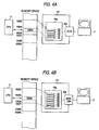
- Figs. 1A and 1B are schematic diagrams for explaining the operation of a scanner in accordance with a first embodiment of the present invention, in which Fig. 1A illustrates a state in which a SCSI-compatible interface unit has been mounted, and Fig. 1B illustrates a state in which an IEEE 1394-compatible interface unit has been mounted;
- Fig. 2 is a block diagram illustrating a scanner in accordance with a first embodiment of the present invention;
- Fig. 3 is a block diagram illustrating firmware of the scanner in accordance with the first embodiment of the present invention;
- Figs. 4A and 4B are schematic diagrams for explaining the operation of a scanner in accordance with a second embodiment of the present invention, in which Fig. 1A illustrates a state in which the SCSI-compatible interface unit has been mounted, and Fig. 1B illustrates a state in which the IEEE 1394-compatible interface unit has been mounted; and
- Figs. 5A and 5B are schematic diagrams for explaining the operation of a scanner in accordance with a third embodiment of the present invention, in which Fig. 1A illustrates a state in which the SCSI-compatible interface unit has been mounted, and Fig. 1B illustrates a State in which the IEEE 1394-compatible interface unit has been mounted.
-
- Hereafter, a description will be given of embodiments illustrating the mode for carrying out the present invention.
- Fig. 2 shows a configuration of hardware in accordance with a first embodiment to which the present invention is applied to a scanner. A
scanner 1 is a computer peripheral apparatus which transmits image data to acomputer 2 by using an unillustrated CCD. - The
scanner 1 has aCPU 11, areading unit 12, a read only memory (ROM) 13, a random access memory (RAM) 14, and aninterface unit 15. TheCPU 11, thereading unit 12, the read only memory (ROM) 13, the random access memory (RAM) 14, and theinterface unit 15 are stored in an unillustrated casing. Anexternal connection port 15b of theinterface unit 15 is exposed on the outer side of the casing, and is connected to thecomputer 2 by acable 16. - The
reading unit 12 has an unillustrated reciprocatable carriage, and outputs the brightness of each pixel of an original as image data by the CCD stored in the carriage. TheCPU 11 is connected to a controller of such as thereading unit 12 through an unillustrated chip select, and controls theoverall scanner 1. TheRAM 14 temporarily stores the image data outputted from thereading unit 12. TheROM 13 which is a nonvolatile memory is a UV-EPROM, and firmware for operating theCPU 11 is stored therein. The nonvolatile memory may be a flash memory. In a case where the flash memory is used as the nonvolatile memory, and firmware is provided by a computer readable medium such as a floppy disk, the rewriting of the firmware in the state in which the flash memory is mounted on a board becomes possible. In addition, the downloading of firmware becomes possible through a communication line by using a communication means such as the Internet. - The
interface unit 15 has acontroller 15a for controlling the transfer of data between thecomputer 2 and theCPU 11, as well as theexternal connection port 15b. TheCPU 11 controls thecontroller 15a of theinterface unit 15 in accordance with a memory-mapped I/O system. Two kinds of interface units are prepared as interface units which can be mounted in thescanner 1. One is a SCSI-compatible interface unit having a SCSI port, and the other is an IEEE 1394-compatible interface unit having anIEEE 1394 port. The controller of the SCSI-compatible interface unit and the controller of the IEEE 1394-compatible interface unit have mutually different assigned regions in memory space. Namely, the chip selects of theCPU 11 to which the respective controllers are assigned are different. A description has been given above of the configuration of hardware in accordance with the first embodiment. - Fig. 3 shows the configuration of software of the firmware.
Firmware 20 includes amain module 21, an identifyingmodule 22, andinterface modules 23 and 24. - Of the modules for controlling the
CPU 11, themain module 21 is a module which is not dependent on theinterface unit 15, and is a module for operating theCPU 11 to control theoverall scanner 1. - The identifying
module 22 serving as an identifying means is a module which writes a value in a predetermined region of the memory space during the starting of thescanner 1, identifies the type of theinterface unit 15 by its return value, and selects either theinterface module 23 or 24 depending on the type of theinterface unit 15, so as to operate theCPU 11. - Of the modules for controlling the
CPU 11, theinterface modules 23 and 24 serving as controlling means are modules which operate theCPU 11 depending on the type of theinterface unit 15 and mainly cause theCPU 11 to issue a command to thecontroller 15a. The interface module 23 controls the SCSI-compatible interface unit, while theinterface module 24 controls the IEEE 1394-compatible interface unit. A description has been given above of the configuration of software in accordance with the first embodiment. - Next, a description will be given of the operation of the scanner in accordance with the first embodiment.
- When the
scanner 1 is started, theCPU 11 writes data in a predetermined region of the memory space by means of the identifyingmodule 22. When the region where the data is written by theCPU 11 and the region of the memory space assigned to an I/O register of thecontroller 15a coincide with each other, if theCPU 11 reads out the data from that region, a valid return value is acquired. Meanwhile, when the region where the data is written by theCPU 11 and the region of the memory space assigned to the I/O register of thecontroller 15a do not coincide with each other, if theCPU 11 reads out the data from that region, an invalid return value is acquired. - For example, it is assumed that, as shown in Figs. 1A and 1B, an assigned region in the memory space of a
controller 40a of a SCSI-compatible interface unit 40 having aSCSI port 40b is aregion having addresses 10000 through 10004, while an assigned region in the memory space of acontroller 41a of an IEEE 1394-compatible interface unit 41 having anIEEE 1394port 41b is aregion having addresses 20000 through 20004. Further, it is assumed that a region in the memory space where theCPU 11 writes data by means of the identifyingmodule 22 is always a region having anaddress 10000. - (1) As shown in Fig. 1A, in a case where the
SCSI-
compatible interface unit 40 is mounted in thescanner 1, theCPU 11 writes data in a region having theaddress 10000 in the memory space by means of the identifyingmodule 22. Then, when acquiring a return value, theCPU 11 acquires a valid return value. - (2) As shown in Fig. 1B, in a case where the
IEEE 1394-
compatible interface unit 41 is mounted in thescanner 1, theCPU 11 writes data in a region having theaddress 10000 in the memory space by means of the identifyingmodule 22. Then, when acquiring a return value, theCPU 11 acquires an. invalid return value since nothing is connected to the chip select corresponding to the region having theaddresses 10000 to 19999. -
- As described in items (1) and (2) above, if the regions in the memory space which are assigned to I/O registers 30 and 31 of the
controllers compatible interface unit 40 and the IEEE 1394-compatible interface unit 41, return values at the time when the identifyingmodule 22 is executed differ. Accordingly, theCPU 11 identifies the type of the interface unit mounted in thescanner 1 by means of its return value. - When the type of the
interface unit 15 mounted in thescanner 1 is identified, the identifyingmodule 22 operates theCPU 11 on the basis of either module corresponding to the type of theinterface unit 15 between theinterface modules 23 and 24. For this reason, a signal is transmitted from theCPU 11 to thecontroller 15a in accordance with the type of theinterface unit 15, and a signal transmitted from thecontroller 15a is processed by theCPU 11. - With the
scanner 1 in accordance with the first embodiment of the present invention, it is possible to operate theCPU 11 of the scanner in which the SCSI-compatible interface unit or the IEEE 1394-compatible interface unit is mounted by using single firmware. For this reason, it is unnecessary to replace theROM 13 in accordance with the type of the interface unit. Therefore, it is unnecessary to manage the firmware for each type of the interface unit. In addition, since theinterface modules 23 and 24 have sufficiently small data sizes as compared with themain module 21, the amount of memory space consumed by recording a plurality of interface modules in theROM 13 is very small. - In a second embodiment in which the present invention is applied to a scanner, assigned regions in the memory space of the controllers of the interface units are identical between the SCSI-compatible interface unit and the IEEE 1394-compatible interface unit. Hereafter, portions which are substantially identical to those of the first embodiment will be denoted by the same reference numerals, and a description thereof will be omitted.
- In the second embodiment, the SCSI-compatible interface unit and the IEEE 1394-compatible interface unit have the same chip select for connection to the
CPU 11. Namely, their assigned regions in the memory space are identical. Meanwhile, the SCSI-compatible interface unit and the IEEE 1394-compatible interface unit have different numbers of I/O registers of their respective controllers. - The identifying module is a module which writes a value in the memory space assigned to the I/O register of the
controller 15a during the starting of the scanner, identities the type of theinterface unit 15 by its return value, and selects either theinterface module 23 or 24 depending on the type of theinterface unit 15, so as to operate theCPU 11. - Next, a description will be given of the operation of the scanner in accordance with the second embodiment.
- When the scanner is started, the
CPU 11 writes data at a predetermined address in the region assigned to thecontroller 15a in the memory space by means of the identifying module. When an I/O register of thecontroller 15a has been assigned to the region where the data is written by theCPU 11, if theCPU 11 reads out the data from that region, a valid return value is acquired. Meanwhile, when the I/O register of thecontroller 15a has not been assigned to the region where the data is written by theCPU 11, if theCPU 11 reads out the data from that region, an invalid return value is acquired. - For example, it is assumed that, as shown in Figs. 4A and 4B, five registers 32 provided in a
controller 42a of a SCSI-compatible interface unit 42 having aSCSI port 42b is assigned toaddresses 10000 through 10004 in the memory space, while seven registers 33 provided in acontroller 43a of an IEEE 1394-compatible interface unit 43 having anIEEE 1394port 43b is assigned toaddresses 20000 through 20004. Further, it is assumed that theCPU 11 writes data in a region having anaddress 10005 in the memory space by means of the identifying module. - (1) As shown in Fig. 4A, in a case where the
SCSI-
compatible interface unit 42 is mounted in the scanner, theCPU 11 writes data at theaddress 10005 in the memory space by means of the identifying module. Then, when acquiring a return value, theCPU 11 acquires an invalid return value since the I/O register 32 assigned to the region at theaddress 10005 is not present. - (2) As shown in Fig. 4B, in a case where the
IEEE 1394-
compatible interface unit 43 is mounted in the scanner, theCPU 11 writes data at theaddress 10005 in the memory space by means of the identifying module. Then, when acquiring a return value, theCPU 11 acquires a valid return value. -
- As described in items (1) and (2) above, if the numbers of registers 32 and 33 provided in the controllers are changed in advance between the SCSI-compatible interface unit and the IEEE 1394-compatible interface unit, return values at the time when the identifying module is executed differ. Accordingly, the
CPU 11 identifies the type of the interface unit mounted in the scanner by means of its return value. - With the scanner in accordance with the second embodiment of the present invention, even if the regions in the memory space assigned to the interface units of different types are identical, the identifying module is able to identify the types of the interface units. For this reason, it is unnecessary to assign a plurality of chip selects of the
CPU 11 to the controllers of the interface units. Accordingly, the number of controllers other than theinterface unit 15 controlled by theCPU 11 can be increased, as required. - In a third embodiment in which the present invention is applied to a scanner, assigned regions in the memory space of the controllers of the interface units are identical between the SCSI-compatible interface unit and the IEEE 1394-compatible interface unit. Hereafter, portions which are substantially identical to those of the first embodiment will be denoted by the same reference numerals, and a description thereof will be omitted.
- In the third embodiment, the SCSI-compatible interface unit and the IEEE 1394-compatible interface unit have the same chip select for connection to the
CPU 11. Namely, their assigned regions in the memory space are identical. In addition, the SCSI-compatible interface unit and the IEEE 1394-compatible interface unit have the same numbers of registers of their respective controllers. Meanwhile, the attributes of the registers differ from each other. - The identifying module is a module which writes a value in the memory space assigned to the I/O register of the
controller 15a during the starting of the scanner, identifies the type of theinterface unit 15 by its return value, and selects either theinterface module 23 or 24 depending on the type of theinterface unit 15, so as to operate theCPU 11. - Next, a description will be given of the operation of the scanner in accordance with the third embodiment.
- When the scanner is started, the
CPU 11 writes data at a predetermined address in the region assigned to the I/O register of thecontroller 15a in the memory space by means of the identifying module. A return value which differs from the written data is acquired depending on the attribute of the register into which the data is written by theCPU 11. - For example, it is assumed that, as shown in Figs. 5A and 5B, five registers 34 provided in a
controller 44a of a SCSI-compatible interface unit 44 having aSCSI port 44b and five registers 35 provided in acontroller 45a of an IEEE 1394-compatible interface unit 45 having anIEEE 1394port 45b both have 8-bit register lengths, and that the registers 34 and 35 are respectively assigned toaddresses 10000 to 10004 in the memory space. Further, it is assumed that the first two bits of each register 34 are exclusively used for reading, and are always adapted to return values of zeros. Meanwhile, it is assumed that the first four bits of each register 35 are exclusively used for reading, and are always adapted to return values of zeros. - (1) As shown in Fig. 5A, in a case where the
SCSI-
compatible interface unit 44 is mounted in the scanner, theCPU 11 writes data consisting of "00010011" at theaddress 10000 in the memory space by means of the identifying module. Then, when acquiring a return value, theCPU 11 acquires a return value consisting of "00010011". - (2) As shown in Fig. 5B, in a case where the
IEEE 1394-
compatible interface unit 45 is mounted in the scanner, theCPU 11 writes data consisting of "00010011" at theaddress 10000 in the memory space by means of the identifying module. Then, when acquiring a return value, theCPU 11 acquires a return value consisting of "00000011". -
- As described in items (1) and (2) above, if the attributes of registers 34 and 35 provided in the controllers are changed in advance between the SCSI-
compatible interface unit 44 and the IEEE 1394-compatible interface unit 45, return values at the time when the identifying module is executed differ. Accordingly, theCPU 11 identifies the type of theinterface unit 15 mounted in the scanner by means of its return value. In addition to the above-described example, the accessing method for theCPU 11 and the I/O register may be based on word accessing in one interface unit so as to change the attributes of the registers. - With the scanner in accordance with the third embodiment of the present invention, even if the regions in the memory space assigned to the interface units of different types are identical, the identifying module is able to identify the types of the interface units. For this reason, it is unnecessary to assign a plurality of chip selects of the
CPU 11 to the controllers of the interface units. Accordingly, the number of controllers other than theinterface unit 15 controlled by theCPU 11 can be increased. Further, even if the numbers of I/O registers of the interface units of different types are identical, the identifying module is able to identify the type of the interface unit. - In a fourth embodiment in which the present invention is applied to a scanner, assigned regions in the memory space of the controllers of the interface units are identical between the SCSI-compatible interface unit and the IEEE 1394-compatible interface unit. Hereafter, portions which are substantially identical to those of the first embodiment will be denoted by the same reference numerals, and a description thereof will be omitted.
- In the fourth embodiment, the SCSI-compatible interface unit and the IEEE 1394-compatible interface unit have the same chip select for connection to the
CPU 11. Namely, their assigned regions in the memory space are identical. In addition, as for the SCSI-compatible interface unit and the IEEE 1394-compatible interface unit, both the numbers and attributes of the I/O registers of their controllers are the same. Meanwhile, inputs to theinterface unit 15 of theCPU 11 differ. - For example, the input to the terminal of an I/O port Pxx is set to high level for the SCSI-compatible interface unit, while the input to the terminal of an I/O port Pxx is set to low level for the IEEE 1394-compatible interface unit. If the input to the
interface unit 15 of theCPU 11 is thus made different between the SCSI-compatible interface unit and the IEEE 1394-compatible interface unit, the return values at the time when the identifying module is executed differ. Accordingly, it is possible to identify the type of theinterface unit 15 mounted in the scanner by means of its return value. - Although in the first to fourth embodiments a description has been given above of the scanner, the present invention is also applicable to other computer peripheral apparatuses such as a printer.
Claims (12)
- A computer peripheral apparatus, comprising:a central processing unit;a plurality of interface units of different types including controllers which control data transfer between a computer and the central processing unit;a plurality of controlling means, one of which mutually transfers signals between the central processing unit and one of the plurality of interface units; andidentifying means which identifies a type of one of the controllers, and which operates the central processing unit by using one of the plurality of controlling means that corresponds to the one of the controllers.
- A computer peripheral apparatus according to claim 1, wherein the identifying means writes a value in a predetermined region of memory space of the central processing unit, and identities the type of one of the controllers by a return value which is obtained by reading data from the predetermined region of the memory space of the central processing unit.
- A computer peripheral apparatus according to any one of claims 1 and 2, wherein the controllers of the plurality of interface units are assigned to respective regions in the memory space of the central processing unit which are mutually different.
- A computer peripheral apparatus according to any one of claims 1 and 2, wherein the plurality of interface units have registers in the respective controllers, and wherein numbers of the registers are mutually different.
- A computer peripheral apparatus according to any one of claims 1 and 2, wherein the plurality of interface units have registers in the respective controllers, and wherein attributes of the registers are mutually different.
- A computer peripheral apparatus according to any one of claims 1 and 2, wherein the plurality of interface units receive different inputs thereto from the central processing unit.
- A computer readable medium having a program stored thereon for controlling a computer peripheral apparatus which includes a central processing unit and a plurality of interface units of different types including controllers which control data transfer between a computer and the central processing unit, the program comprising the steps of:mutually transferring signals between the central processing unit and one of the plurality of interface units;identifying a type of one of the controllers; andoperating the central processing unit in accordance with the type of one of the controllers identified in the identifying step.
- A computer readable medium according to claim 7, wherein the identifying step comprising:writing a value in a predetermined region of memory space of the central processing unit; andidentifying the type of one of the controllers by a return value which is obtained by reading data from the predetermined region of the memory space of the central processing unit.
- A data signal for storing the program according to any one of claims 7 and 8 in the computer.
- A computer readable medium having a program stored thereon for controlling a computer peripheral apparatus which includes a central processing unit, a plurality of interface units of different types including controllers which control data transfer between a computer and the central processing unit, a plurality of controlling means, and identifying means, wherein the program causes one of the plurality of controlling means to mutually transfer a signal between the central processing unit and one of the plurality of interface units, and wherein the program causes the identifying means to identify a type of one of the controllers and operate the central processing unit by using one of the plurality of controlling means that corresponds to the one of the controllers.
- A computer readable medium according to claim 10, wherein the program causes the identifying means to write a value in a predetermined region of memory space of the central processing unit and identify the type of one of the controllers by a return value which is obtained by reading data from the predetermined region of the memory space of the central processing unit.
- A data signal for storing the program according to any one of claims 10 and 11 in the computer.
Applications Claiming Priority (2)
| Application Number | Priority Date | Filing Date | Title |
|---|---|---|---|
| JP11191635A JP2001022680A (en) | 1999-07-06 | 1999-07-06 | Computer peripheral device |
| JP19163599 | 1999-07-06 |
Publications (2)
| Publication Number | Publication Date |
|---|---|
| EP1067462A1 true EP1067462A1 (en) | 2001-01-10 |
| EP1067462B1 EP1067462B1 (en) | 2007-03-07 |
Family
ID=16277945
Family Applications (1)
| Application Number | Title | Priority Date | Filing Date |
|---|---|---|---|
| EP00114066A Expired - Lifetime EP1067462B1 (en) | 1999-07-06 | 2000-07-06 | A computer peripheral apparatus and a computer readable medium having a program for controlling the computer peripheral apparatus |
Country Status (5)
| Country | Link |
|---|---|
| US (1) | US6789138B1 (en) |
| EP (1) | EP1067462B1 (en) |
| JP (1) | JP2001022680A (en) |
| AT (1) | ATE356383T1 (en) |
| DE (1) | DE60033740T2 (en) |
Families Citing this family (2)
| Publication number | Priority date | Publication date | Assignee | Title |
|---|---|---|---|---|
| US6728801B2 (en) * | 2001-06-29 | 2004-04-27 | Intel Corporation | Method and apparatus for period promotion avoidance for hubs |
| US8060662B2 (en) * | 2007-12-17 | 2011-11-15 | Ricoh Company, Ltd. | Recording control apparatus, recording control method, and computer program product |
Citations (4)
| Publication number | Priority date | Publication date | Assignee | Title |
|---|---|---|---|---|
| JPS5952333A (en) * | 1982-09-17 | 1984-03-26 | Hitachi Ltd | System extending system |
| JPH04177744A (en) * | 1990-11-09 | 1992-06-24 | Omron Corp | Method for discriminating kind of memory |
| US5274765A (en) * | 1989-04-17 | 1993-12-28 | Bull S.A | Multifunctional coupler for connecting a central processing unit of a computer to one or more peripheral devices |
| EP0686937A2 (en) * | 1994-05-31 | 1995-12-13 | Canon Kabushiki Kaisha | Printing control apparatus and control program selecting method |
Family Cites Families (14)
| Publication number | Priority date | Publication date | Assignee | Title |
|---|---|---|---|---|
| US4476522A (en) * | 1981-03-09 | 1984-10-09 | International Business Machines Corporation | Programmable peripheral processing controller with mode-selectable address register sequencing |
| DE3586557D1 (en) * | 1984-10-26 | 1992-10-01 | Ibm | DATA PROCESSING DEVICE WITH FIXED ADDRESS SPACE AND VARIABLE MEMORY. |
| JPS6431217A (en) | 1987-07-27 | 1989-02-01 | Sharp Kk | Method for selecting interface for computer equipment |
| US5842041A (en) * | 1994-05-20 | 1998-11-24 | Advanced Micro Devices, Inc. | Computer system employing a control signal indicative of whether address is within address space of devices on processor local bus |
| WO1996038773A2 (en) * | 1995-05-26 | 1996-12-05 | National Semiconductor Corporation | Integrated primary bus and secondary bus controller with reduced pin count |
| US5835760A (en) * | 1995-10-13 | 1998-11-10 | Texas Instruments Incorporated | Method and arrangement for providing BIOS to a host computer |
| US5872998A (en) * | 1995-11-21 | 1999-02-16 | Seiko Epson Corporation | System using a primary bridge to recapture shared portion of a peripheral memory of a peripheral device to provide plug and play capability |
| JP3403284B2 (en) * | 1995-12-14 | 2003-05-06 | インターナショナル・ビジネス・マシーンズ・コーポレーション | Information processing system and control method thereof |
| JPH10171957A (en) * | 1996-12-04 | 1998-06-26 | Murata Mfg Co Ltd | Cis switching feature for pc card |
| US5944806A (en) * | 1997-09-26 | 1999-08-31 | Hewlett-Packard Company | Microprocessor with versatile addressing |
| US5928347A (en) * | 1997-11-18 | 1999-07-27 | Shuttle Technology Group Ltd. | Universal memory card interface apparatus |
| JPH11259605A (en) * | 1998-01-08 | 1999-09-24 | Tdk Corp | Pc card |
| US6480948B1 (en) * | 1999-06-24 | 2002-11-12 | Cirrus Logic, Inc. | Configurable system memory map |
| US6446139B1 (en) * | 1999-06-28 | 2002-09-03 | Adaptec, Inc. | Multiple chip single image BIOS |
-
1999
- 1999-07-06 JP JP11191635A patent/JP2001022680A/en active Pending
-
2000
- 2000-07-05 US US09/610,290 patent/US6789138B1/en not_active Expired - Lifetime
- 2000-07-06 EP EP00114066A patent/EP1067462B1/en not_active Expired - Lifetime
- 2000-07-06 AT AT00114066T patent/ATE356383T1/en not_active IP Right Cessation
- 2000-07-06 DE DE60033740T patent/DE60033740T2/en not_active Expired - Lifetime
Patent Citations (4)
| Publication number | Priority date | Publication date | Assignee | Title |
|---|---|---|---|---|
| JPS5952333A (en) * | 1982-09-17 | 1984-03-26 | Hitachi Ltd | System extending system |
| US5274765A (en) * | 1989-04-17 | 1993-12-28 | Bull S.A | Multifunctional coupler for connecting a central processing unit of a computer to one or more peripheral devices |
| JPH04177744A (en) * | 1990-11-09 | 1992-06-24 | Omron Corp | Method for discriminating kind of memory |
| EP0686937A2 (en) * | 1994-05-31 | 1995-12-13 | Canon Kabushiki Kaisha | Printing control apparatus and control program selecting method |
Non-Patent Citations (2)
| Title |
|---|
| PATENT ABSTRACTS OF JAPAN vol. 008, no. 153 (P - 287) 17 July 1984 (1984-07-17) * |
| PATENT ABSTRACTS OF JAPAN vol. 016, no. 486 (E - 1276) 8 October 1992 (1992-10-08) * |
Also Published As
| Publication number | Publication date |
|---|---|
| ATE356383T1 (en) | 2007-03-15 |
| EP1067462B1 (en) | 2007-03-07 |
| US6789138B1 (en) | 2004-09-07 |
| JP2001022680A (en) | 2001-01-26 |
| DE60033740T2 (en) | 2007-12-06 |
| DE60033740D1 (en) | 2007-04-19 |
Similar Documents
| Publication | Publication Date | Title |
|---|---|---|
| US4475155A (en) | I/O Adapter with direct memory access to I/O control information | |
| US7839527B2 (en) | Data control apparatus, data control method thereof and image forming apparatus | |
| US5778195A (en) | PC card | |
| KR100196333B1 (en) | Dma data transferring method using free loading of dma instruction | |
| KR19990030283A (en) | Storage devices, data processing systems and data recording and reading methods | |
| JP2000105725A (en) | Chip enable signal generating circuit, and memory device | |
| US6954815B2 (en) | Microcomputer with universal serial bus interface circuit and method of controlling the same | |
| US11409679B2 (en) | System component and use of a system component | |
| JPS63116258A (en) | Data processing system | |
| US6789138B1 (en) | Computer peripheral apparatus and a computer readable medium having a program for controlling the computer peripheral apparatus | |
| JP3673015B2 (en) | Peripheral device identification method in semiconductor device | |
| US6742056B2 (en) | Semiconductor device and method for initializing interface card using serial EEPROM | |
| US20040042041A1 (en) | Image forming device | |
| KR20070060854A (en) | Multi-channel direct memory access controller | |
| US20030167371A1 (en) | Memory rewriting apparatus | |
| CN100386748C (en) | Method and system for chip selecting of peripheral device in singe board computer | |
| US6178003B1 (en) | Method of and apparatus for transmitting printer control file to printer | |
| JPH09259068A (en) | Extended input and output interface | |
| US5892972A (en) | Method of constructing a plug and play compatible bus card which allows for mass production of the bus card | |
| JP4723334B2 (en) | DMA transfer system | |
| US7369173B2 (en) | Image processing apparatus and control method therefor | |
| JPH1173368A (en) | Memory module, method for control information processor and recording medium | |
| JP2006011926A (en) | Serial data transfer system, serial data transfer device, serial data transfer method and image forming apparatus | |
| US6480296B1 (en) | Image processing apparatus and memory access method therefor | |
| US5548778A (en) | System for assigning device to be connected to computer when address from computer is effective by comparing address for entire memory space and found coincided |
Legal Events
| Date | Code | Title | Description |
|---|---|---|---|
| PUAI | Public reference made under article 153(3) epc to a published international application that has entered the european phase |
Free format text: ORIGINAL CODE: 0009012 |
|
| AK | Designated contracting states |
Kind code of ref document: A1 Designated state(s): AT BE CH CY DE DK ES FI FR GB GR IE IT LI LU MC NL PT SE |
|
| AX | Request for extension of the european patent |
Free format text: AL;LT;LV;MK;RO;SI |
|
| 17P | Request for examination filed |
Effective date: 20010426 |
|
| 17Q | First examination report despatched |
Effective date: 20010713 |
|
| AKX | Designation fees paid |
Free format text: AT BE CH CY DE DK ES FI FR GB GR IE IT LI LU MC NL PT SE |
|
| GRAP | Despatch of communication of intention to grant a patent |
Free format text: ORIGINAL CODE: EPIDOSNIGR1 |
|
| GRAS | Grant fee paid |
Free format text: ORIGINAL CODE: EPIDOSNIGR3 |
|
| GRAA | (expected) grant |
Free format text: ORIGINAL CODE: 0009210 |
|
| AK | Designated contracting states |
Kind code of ref document: B1 Designated state(s): AT BE CH CY DE DK ES FI FR GB GR IE IT LI LU MC NL PT SE |
|
| PG25 | Lapsed in a contracting state [announced via postgrant information from national office to epo] |
Ref country code: NL Free format text: LAPSE BECAUSE OF FAILURE TO SUBMIT A TRANSLATION OF THE DESCRIPTION OR TO PAY THE FEE WITHIN THE PRESCRIBED TIME-LIMIT Effective date: 20070307 Ref country code: AT Free format text: LAPSE BECAUSE OF FAILURE TO SUBMIT A TRANSLATION OF THE DESCRIPTION OR TO PAY THE FEE WITHIN THE PRESCRIBED TIME-LIMIT Effective date: 20070307 Ref country code: CH Free format text: LAPSE BECAUSE OF FAILURE TO SUBMIT A TRANSLATION OF THE DESCRIPTION OR TO PAY THE FEE WITHIN THE PRESCRIBED TIME-LIMIT Effective date: 20070307 Ref country code: LI Free format text: LAPSE BECAUSE OF FAILURE TO SUBMIT A TRANSLATION OF THE DESCRIPTION OR TO PAY THE FEE WITHIN THE PRESCRIBED TIME-LIMIT Effective date: 20070307 Ref country code: BE Free format text: LAPSE BECAUSE OF FAILURE TO SUBMIT A TRANSLATION OF THE DESCRIPTION OR TO PAY THE FEE WITHIN THE PRESCRIBED TIME-LIMIT Effective date: 20070307 Ref country code: FI Free format text: LAPSE BECAUSE OF FAILURE TO SUBMIT A TRANSLATION OF THE DESCRIPTION OR TO PAY THE FEE WITHIN THE PRESCRIBED TIME-LIMIT Effective date: 20070307 |
|
| REG | Reference to a national code |
Ref country code: GB Ref legal event code: FG4D |
|
| REG | Reference to a national code |
Ref country code: CH Ref legal event code: EP |
|
| REF | Corresponds to: |
Ref document number: 60033740 Country of ref document: DE Date of ref document: 20070419 Kind code of ref document: P |
|
| REG | Reference to a national code |
Ref country code: IE Ref legal event code: FG4D |
|
| PG25 | Lapsed in a contracting state [announced via postgrant information from national office to epo] |
Ref country code: SE Free format text: LAPSE BECAUSE OF FAILURE TO SUBMIT A TRANSLATION OF THE DESCRIPTION OR TO PAY THE FEE WITHIN THE PRESCRIBED TIME-LIMIT Effective date: 20070607 |
|
| PG25 | Lapsed in a contracting state [announced via postgrant information from national office to epo] |
Ref country code: ES Free format text: LAPSE BECAUSE OF FAILURE TO SUBMIT A TRANSLATION OF THE DESCRIPTION OR TO PAY THE FEE WITHIN THE PRESCRIBED TIME-LIMIT Effective date: 20070618 |
|
| PG25 | Lapsed in a contracting state [announced via postgrant information from national office to epo] |
Ref country code: PT Free format text: LAPSE BECAUSE OF FAILURE TO SUBMIT A TRANSLATION OF THE DESCRIPTION OR TO PAY THE FEE WITHIN THE PRESCRIBED TIME-LIMIT Effective date: 20070807 |
|
| ET | Fr: translation filed | ||
| NLV1 | Nl: lapsed or annulled due to failure to fulfill the requirements of art. 29p and 29m of the patents act | ||
| REG | Reference to a national code |
Ref country code: CH Ref legal event code: PL |
|
| PLBE | No opposition filed within time limit |
Free format text: ORIGINAL CODE: 0009261 |
|
| STAA | Information on the status of an ep patent application or granted ep patent |
Free format text: STATUS: NO OPPOSITION FILED WITHIN TIME LIMIT |
|
| PG25 | Lapsed in a contracting state [announced via postgrant information from national office to epo] |
Ref country code: DK Free format text: LAPSE BECAUSE OF FAILURE TO SUBMIT A TRANSLATION OF THE DESCRIPTION OR TO PAY THE FEE WITHIN THE PRESCRIBED TIME-LIMIT Effective date: 20070307 |
|
| 26N | No opposition filed |
Effective date: 20071210 |
|
| PG25 | Lapsed in a contracting state [announced via postgrant information from national office to epo] |
Ref country code: IT Free format text: LAPSE BECAUSE OF FAILURE TO SUBMIT A TRANSLATION OF THE DESCRIPTION OR TO PAY THE FEE WITHIN THE PRESCRIBED TIME-LIMIT Effective date: 20070307 Ref country code: MC Free format text: LAPSE BECAUSE OF NON-PAYMENT OF DUE FEES Effective date: 20070731 Ref country code: GR Free format text: LAPSE BECAUSE OF FAILURE TO SUBMIT A TRANSLATION OF THE DESCRIPTION OR TO PAY THE FEE WITHIN THE PRESCRIBED TIME-LIMIT Effective date: 20070608 |
|
| PG25 | Lapsed in a contracting state [announced via postgrant information from national office to epo] |
Ref country code: IE Free format text: LAPSE BECAUSE OF NON-PAYMENT OF DUE FEES Effective date: 20070706 |
|
| PG25 | Lapsed in a contracting state [announced via postgrant information from national office to epo] |
Ref country code: CY Free format text: LAPSE BECAUSE OF FAILURE TO SUBMIT A TRANSLATION OF THE DESCRIPTION OR TO PAY THE FEE WITHIN THE PRESCRIBED TIME-LIMIT Effective date: 20070307 |
|
| PG25 | Lapsed in a contracting state [announced via postgrant information from national office to epo] |
Ref country code: LU Free format text: LAPSE BECAUSE OF NON-PAYMENT OF DUE FEES Effective date: 20070706 |
|
| REG | Reference to a national code |
Ref country code: FR Ref legal event code: PLFP Year of fee payment: 17 |
|
| REG | Reference to a national code |
Ref country code: FR Ref legal event code: PLFP Year of fee payment: 18 |
|
| PGFP | Annual fee paid to national office [announced via postgrant information from national office to epo] |
Ref country code: FR Payment date: 20170613 Year of fee payment: 18 |
|
| PGFP | Annual fee paid to national office [announced via postgrant information from national office to epo] |
Ref country code: DE Payment date: 20170627 Year of fee payment: 18 Ref country code: GB Payment date: 20170705 Year of fee payment: 18 |
|
| REG | Reference to a national code |
Ref country code: DE Ref legal event code: R119 Ref document number: 60033740 Country of ref document: DE |
|
| GBPC | Gb: european patent ceased through non-payment of renewal fee |
Effective date: 20180706 |
|
| PG25 | Lapsed in a contracting state [announced via postgrant information from national office to epo] |
Ref country code: DE Free format text: LAPSE BECAUSE OF NON-PAYMENT OF DUE FEES Effective date: 20190201 Ref country code: FR Free format text: LAPSE BECAUSE OF NON-PAYMENT OF DUE FEES Effective date: 20180731 Ref country code: GB Free format text: LAPSE BECAUSE OF NON-PAYMENT OF DUE FEES Effective date: 20180706 |