EP1069419A2 - Pressure sensor and method of manufacturing the same - Google Patents
Pressure sensor and method of manufacturing the same Download PDFInfo
- Publication number
- EP1069419A2 EP1069419A2 EP00250241A EP00250241A EP1069419A2 EP 1069419 A2 EP1069419 A2 EP 1069419A2 EP 00250241 A EP00250241 A EP 00250241A EP 00250241 A EP00250241 A EP 00250241A EP 1069419 A2 EP1069419 A2 EP 1069419A2
- Authority
- EP
- European Patent Office
- Prior art keywords
- glass base
- bonding
- sensor
- glass
- electrodes
- Prior art date
- Legal status (The legal status is an assumption and is not a legal conclusion. Google has not performed a legal analysis and makes no representation as to the accuracy of the status listed.)
- Granted
Links
Images

Classifications
-
- G—PHYSICS
- G01—MEASURING; TESTING
- G01L—MEASURING FORCE, STRESS, TORQUE, WORK, MECHANICAL POWER, MECHANICAL EFFICIENCY, OR FLUID PRESSURE
- G01L9/00—Measuring steady of quasi-steady pressure of fluid or fluent solid material by electric or magnetic pressure-sensitive elements; Transmitting or indicating the displacement of mechanical pressure-sensitive elements, used to measure the steady or quasi-steady pressure of a fluid or fluent solid material, by electric or magnetic means
-
- G—PHYSICS
- G01—MEASURING; TESTING
- G01L—MEASURING FORCE, STRESS, TORQUE, WORK, MECHANICAL POWER, MECHANICAL EFFICIENCY, OR FLUID PRESSURE
- G01L19/00—Details of, or accessories for, apparatus for measuring steady or quasi-steady pressure of a fluent medium insofar as such details or accessories are not special to particular types of pressure gauges
- G01L19/0061—Electrical connection means
- G01L19/0069—Electrical connection means from the sensor to its support
-
- G—PHYSICS
- G01—MEASURING; TESTING
- G01L—MEASURING FORCE, STRESS, TORQUE, WORK, MECHANICAL POWER, MECHANICAL EFFICIENCY, OR FLUID PRESSURE
- G01L19/00—Details of, or accessories for, apparatus for measuring steady or quasi-steady pressure of a fluent medium insofar as such details or accessories are not special to particular types of pressure gauges
- G01L19/14—Housings
- G01L19/147—Details about the mounting of the sensor to support or covering means
-
- H—ELECTRICITY
- H01—ELECTRIC ELEMENTS
- H01L—SEMICONDUCTOR DEVICES NOT COVERED BY CLASS H10
- H01L2224/00—Indexing scheme for arrangements for connecting or disconnecting semiconductor or solid-state bodies and methods related thereto as covered by H01L24/00
- H01L2224/01—Means for bonding being attached to, or being formed on, the surface to be connected, e.g. chip-to-package, die-attach, "first-level" interconnects; Manufacturing methods related thereto
- H01L2224/42—Wire connectors; Manufacturing methods related thereto
- H01L2224/47—Structure, shape, material or disposition of the wire connectors after the connecting process
- H01L2224/48—Structure, shape, material or disposition of the wire connectors after the connecting process of an individual wire connector
- H01L2224/4805—Shape
- H01L2224/4809—Loop shape
- H01L2224/48091—Arched
Definitions
- the present invention relates to an electrostatic capacitive or piezoelectric pressure sensor and a method of manufacturing the same and, more particularly, to a bonding structure and bonding method for a sensor chip and sensor package employed when electrodes of the sensor chip are extracted from the lower side of the sensor chip.
- an electrostatic capacitive pressure sensor As a conventional pressure sensor, an electrostatic capacitive pressure sensor is known.
- the electrostatic capacitive pressure sensor has a substrate with a recess, a diaphragm supported on a substrate at its periphery and arranged on the recess, a stationary electrode formed on the bottom surface of the recess, and a movable electrode formed on the diaphragm to oppose the stationary electrode.
- the pressure sensor having this arrangement when the diaphragm deforms upon reception of an external pressure, the distance between the movable and stationary electrodes changes to change the electrostatic capacitance between them. The pressure applied to the diaphragm is measured on the basis of this change in electrostatic capacitance.
- a piezoelectric pressure sensor As another pressure sensor, a piezoelectric pressure sensor is known.
- the piezoelectric pressure sensor has, in place of an electrode, a strain gauge with a piezoresistive effect on a semiconductor diaphragm.
- the strain gauge is deformed by a pressure applied to the diaphragm.
- the pressure is measured by detecting a change in resistance of the strain gauge produced by the piezoresistive effect.
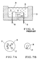
- a sensor chip 23 is mounted on a cylindrical glass base 22 in a cylindrical metal package 21 sealed by a corrosion-resistant diaphragm 24, and a sealed liquid 25 such as silicone oil is sealed in the metal package 21.
- the pressure is transmitted to the sensor chip 23 by this structure.
- the electrical connection between the sensor chip 23 and the outside is realized by connecting electrode extraction pins 26 hermetically sealed with glass and electrodes formed on the upper surface of the sensor chip 23 with wires 27.
- the sealed liquid may be eliminated.
- corrosion of the sensor chip and physical impact applied to the sensor chip pose problems. For this reason, electrodes and wires cannot be formed on the upper surface of the chip, and the electrodes are extracted from the lower side of the sensor chip.
- the electrodes cannot be extracted from the lower side of the sensor chip. More specifically, when the sensor chip extends to the lower surface of the metal package and the electrodes are extracted from the lower side of the sensor chip, stress is likely to occur in the bonding portion between the sensor chip and the seal surface of the package. For this reason, the diaphragm of the sensor chip need be set away from the seal surface, leading to an increase in size of the sensor.
- the measuring method shown in Fig. 6 realizes this by mounting the sensor chip 23 on the glass base 22 and bonding the glass base 22 to the metal package 21. With this method, the number of manufacturing steps increases. Also, the number of bonding surfaces increases, thereby degrading the yield.
- a pressure sensor comprising a cylindrical sensor package, a glass base seal-bonded to an inner surface of the sensor package to close a space in the sensor package, a sensor chip mounted on the glass base and having electrodes and a metal bonding portion on a surface thereof opposing the glass base, the bonding portion being die-bonded to a surface of the glass base, and lead members arranged to oppose the electrodes and buried to extend through the glass base, one end of each of the lead members exposed from the surface of the glass surface being electrically bonded to a corresponding one of the electrodes.
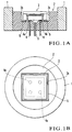
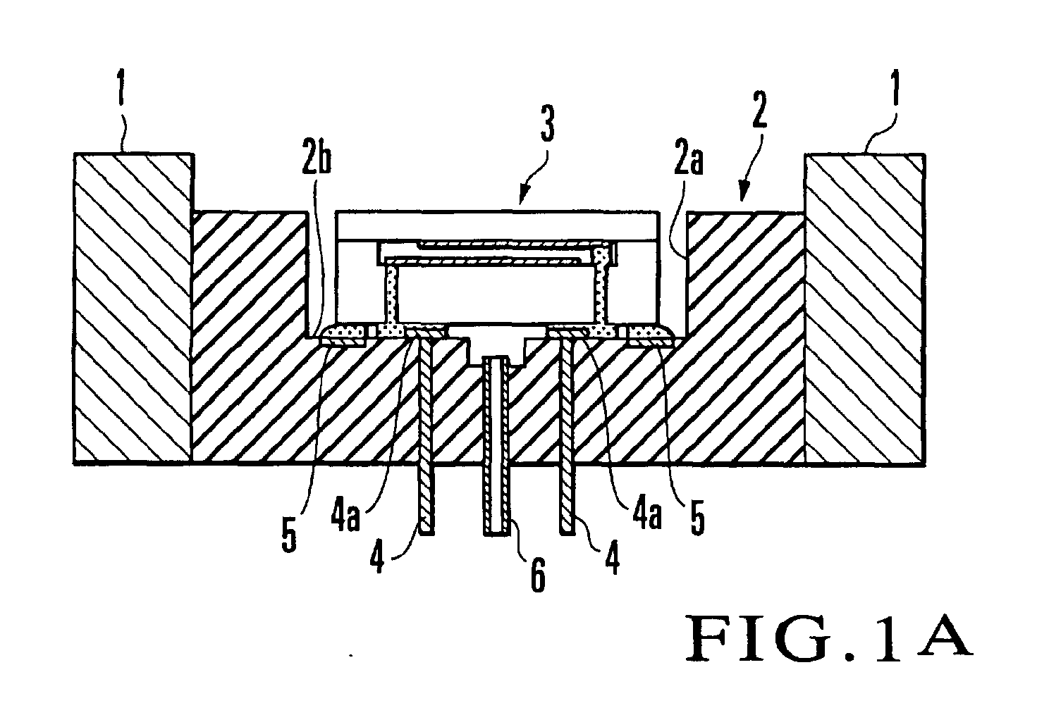
- Fig. 1A shows a pressure sensor according to an embodiment of the present invention
- Fig. 1B shows the pressure sensor shown in Fig. 1A
- a cylindrical sensor package 1 is made of corrosion-resistant metal such as stainless steel.
- a thick disk-like glass base 2 is fitted on the inner wall of the sensor package 1.
- the glass base 2 has a square recess 2a at its central portion, and a support 2b on the bottom surface of the recess 2a to support a sensor chip (to be described later).
- a sensor chip 3 is mounted on the support 2b of the glass base 2.
- Electrode extraction pins (to be referred to as electrode pins hereinafter) 4 are buried in the glass base 2 to extend through the support 2b, and serve as lead members.
- a metal plate 5 is buried slightly inside the support 2b of the glass base 2 to correspond to the periphery of the sensor chip 3.
- An atmospheric pressure introduction pipe 6 is buried in the glass base 2 to extend through the central portion of the support 2b.
- the electrode pins 4 respectively have heads 4a to be exposed from the support 2b of the glass base 2.
- the metal plate 5 is made of an Fe-Cr alloy, Fe-Ni-Cr alloy, Fe-Ni alloy, Fe-Ni-Co alloy, Ni-group alloy, or the like, and forms a square frame.
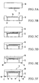
- a method of manufacturing the pressure sensor described above will be described with reference to Figs. 2A to 2C, Figs. 3A to 3F, and Fig. 4. First, how to fabricate the package on which the sensor chip 3 is to be mounted will be described.
- the thick disk-like (bottomed cylindrical) glass base 2 with a recess 2a is molded.
- the electrode pins 4, the metal plate 5 having the square shape, and the atmospheric pressure introduction pipe 6 are buried in the support 2b of the glass base 2 by integral molding.
- the electrode pins 4 are buried such that their heads 4a are exposed from the support 2b of the glass base 2 and their distal ends project from the lower side of the glass base 2.
- the glass base 2 is inserted in the sensor package 1 and heated.
- the glass base 2 is thus fused so that it is hermetically bonded to the sensor package 1.
- solder coating is performed to form solder portions 7 on the heads 4a of the electrode pins 4 and the metal plate 5. Fabrication of the sensor package 1 is ended in this manner.
- a conductive thin film is formed on the lower surface of a sapphire first substrate 10 on the diaphragm side and patterned to form a movable electrode 11 with a predetermined shape.
- a recess 13 is formed in the center of the upper surface of a sapphire second substrate 12 by wet or dry etching, and through holes 14 for electrode leads are formed in the recess 13, so that the recess 13 and the outside communicate with each other through the through holes 14.
- a conductive thin film is formed at the center of the bottom surface of the recess 13 and patterned to form a stationary electrode 15 with a predetermined shape.
- the conductive thin films on the substrates 10 and 12 can be formed by CVD (Chemical Vapor Deposition), vacuum deposition, sputtering, or the like.
- the first and second substrates 10 and 12 are overlaid in tight contact with each other, are loaded in a vacuum furnace, and are heated in vacuum, so that they are tightly bonded to each other.
- the first substrate 10 is polished to a predetermined thickness to form a diaphragm. This diaphragm surface may be formed by etching back the first substrate 10 in accordance with wet etching, dry etching, or the like.
- a bonding portion 16 comprised of a metal film is formed along the periphery of the lower surface of the second substrate 12 by vacuum deposition to have a square frame-like shape.
- solder coating is performed to form a solder portion 17 on the bonding portion 16. During solder coating, solder also fills the through holes 14, so that electrodes 18 connected to the movable electrode 11 and electrodes 19 connected to the stationary electrode 15 are formed inside the bonding portion 16.
- the bonding portion 16 need not form a square frame, but a plurality of bonding portions 16 may be formed at predetermined intervals.
- preplaced brazing in a solder furnace is performed. In this manner, fabrication of the sensor chip 3 is ended.
- the sensor chip 3 and glass base 2 are aligned such that the bonding portion 16 of the sensor chip 3, and the electrodes 18 and 19 of the sensor chip 3 substantially, respectively oppose the metal plate 5 of the glass base 2 and the heads 4a of the electrode pins 4 of the glass base 2.
- the aligned sensor chip 3 is placed on the glass base 2.
- the sensor chip 3 and glass base 2 are then heated to fuse solder, thereby soldering them with each other. In this manner, fabrication of the pressure sensor is ended.
- the glass base 2 is seal-bonded to the inner wall of the sensor package 1 to close the space in the sensor package 1, heat stress from the sensor package 1 can be canceled by the whole glass base 2. Since the electrode pins 4 are buried during fabrication of the glass base 2, the electrodes 18 and 19 of the sensor chip 3 can be connected to the heads 4a of the electrode pins 4 by only fixing the sensor chip 3 to the glass base 2.
- the number of manufacturing steps increases by one. According to the above embodiment, since the electrode pins 4 and metal plate 5 are buried in the glass base 2 by integral molding during fabrication of the glass base 2, the number of steps does not increase.
- the distances dl and d2 between the electrode extraction pins, and the insulating distance cannot be decreased.
- this conventional problem does not exist basically, and the pressure sensor can be downsized.
- this electrical bond may be attained by brazing or conductive glass bonding. While soldering is performed for die bonding of the bonding portion 16 and the surface of the glass base 2, this die bonding may be attained by brazing or glass encapsulation. To fix the sensor chip 3 and to extract the electrodes simultaneously, electrical bonding and die bonding described above must be performed in accordance with the same bonding method. When the metal plate 5 is to be buried in the surface of the glass base 2 opposing the bonding portion 16, it can be achieved by only soldering and brazing among the bonding methods described above.
- the material of the glass base 2 includes sapphire glass.
- the electrode extraction pins and electrodes are bonded by soldering, and the bonding portion and the surface of the glass base are bonded by soldering, so that the sensor chip can be fixed and the electrodes can be extracted simultaneously.
- the manufacturing steps are simplified, thereby improving the yield.
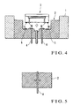
- the resultant pressure sensor can be more downsized than a conventional pressure sensor in which electrode extraction pins are fixed to a metal sensor package with a glass hermetic seal. Since the center-collared pins can be used as the electrode extraction pins, a higher pressure resistance of the pins can be ensured in the longitudinal direction, largely contributing to an increase in pressure resistance of the package.
- the electrode extraction pins and the metal plate can be buried simultaneously during molding of the glass base, no soldering metallizing portion need be formed on the glass base, and the number of manufacturing steps does not increase. Also, a larger fixing force than that obtained by metallizing can be expected.
Abstract
Description
- The present invention relates to an electrostatic capacitive or piezoelectric pressure sensor and a method of manufacturing the same and, more particularly, to a bonding structure and bonding method for a sensor chip and sensor package employed when electrodes of the sensor chip are extracted from the lower side of the sensor chip.
- As a conventional pressure sensor, an electrostatic capacitive pressure sensor is known. The electrostatic capacitive pressure sensor has a substrate with a recess, a diaphragm supported on a substrate at its periphery and arranged on the recess, a stationary electrode formed on the bottom surface of the recess, and a movable electrode formed on the diaphragm to oppose the stationary electrode. In the pressure sensor having this arrangement, when the diaphragm deforms upon reception of an external pressure, the distance between the movable and stationary electrodes changes to change the electrostatic capacitance between them. The pressure applied to the diaphragm is measured on the basis of this change in electrostatic capacitance.
- As another pressure sensor, a piezoelectric pressure sensor is known. The piezoelectric pressure sensor has, in place of an electrode, a strain gauge with a piezoresistive effect on a semiconductor diaphragm. The strain gauge is deformed by a pressure applied to the diaphragm. The pressure is measured by detecting a change in resistance of the strain gauge produced by the piezoresistive effect.
- To measure a pressure by using the pressure sensor described above, as shown in Fig. 6, a
sensor chip 23 is mounted on acylindrical glass base 22 in acylindrical metal package 21 sealed by a corrosion-resistant diaphragm 24, and a sealedliquid 25 such as silicone oil is sealed in themetal package 21. The pressure is transmitted to thesensor chip 23 by this structure. The electrical connection between thesensor chip 23 and the outside is realized by connectingelectrode extraction pins 26 hermetically sealed with glass and electrodes formed on the upper surface of thesensor chip 23 withwires 27. - With the arrangement as shown in Fig. 6, since the volume of the sealed
liquid 25 changes in accordance with a temperature change, errors occur in transmission of the pressure, making it difficult to measure the pressure at high precision. If thediaphragm 24 is torn and the sealedliquid 25 leaks, a measurement target liquid (gas) is contaminated by the sealedliquid 25. Thus, this arrangement is difficult to use for sanitary applications. - In order to solve these problems, the sealed liquid may be eliminated. In this case, as the sensor chip comes into direct contact with the measurement target liquid, corrosion of the sensor chip and physical impact applied to the sensor chip pose problems. For this reason, electrodes and wires cannot be formed on the upper surface of the chip, and the electrodes are extracted from the lower side of the sensor chip.
- In the conventional pressure sensor, however, if the sensor chip is fixed, the electrodes cannot be extracted from the lower side of the sensor chip. More specifically, when the sensor chip extends to the lower surface of the metal package and the electrodes are extracted from the lower side of the sensor chip, stress is likely to occur in the bonding portion between the sensor chip and the seal surface of the package. For this reason, the diaphragm of the sensor chip need be set away from the seal surface, leading to an increase in size of the sensor.
- In the pressure sensor, thermal stress from the metal package should not be transmitted to the sensor chip as much as possible. The measuring method shown in Fig. 6 realizes this by mounting the
sensor chip 23 on theglass base 22 and bonding theglass base 22 to themetal package 21. With this method, the number of manufacturing steps increases. Also, the number of bonding surfaces increases, thereby degrading the yield. - In the pressure sensor shown in Fig. 6, since the
electrode extraction pins 26 are fixed to themetal package 21 with a glasshermetic seal 27, distances d1 and d2 between theelectrode extraction pins 26 cannot be decreased because holes must be formed. Also, the insulating distance (the size of the glass hermetic seal 27) d3 cannot be decreased. - It is an object of the present invention to provide a pressure sensor which, in a structure where electrodes are extracted from the lower side of a sensor chip, the sensor chip can be fixed and the electrodes can be extracted simultaneously while improving the yield, and a method of manufacturing the same.
- In order to achieve the above object, according to the present invention, there is provided a pressure sensor comprising a cylindrical sensor package, a glass base seal-bonded to an inner surface of the sensor package to close a space in the sensor package, a sensor chip mounted on the glass base and having electrodes and a metal bonding portion on a surface thereof opposing the glass base, the bonding portion being die-bonded to a surface of the glass base, and lead members arranged to oppose the electrodes and buried to extend through the glass base, one end of each of the lead members exposed from the surface of the glass surface being electrically bonded to a corresponding one of the electrodes.
-
- Figs. 1A and 1B are sectional and plan views, respectively, of a pressure sensor according to an embodiment of the present invention;
- Figs. 2A to 2C are sectional views showing the steps in fabricating a glass base shown in Figs. lA and 1B;
- Figs. 3A to 3F are views showing the steps in fabricating a sensor chip shown in Figs. 1A and 1B;
- Fig. 4 is a sectional view showing a method of manufacturing the pressure sensor shown in Figs. lA and 1B;
- Fig. 5 is a sectional view of a glass base employed when a center-collared pin is used as an electrode extraction pin;
- Fig. 6 is a sectional view of a conventional pressure sensor; and
- Figs. 7A and 7B are plan views of the electrode portion of the pressure sensor shown in Fig. 6.
-
- The present invention will be described in detail with reference to the accompanying drawings.
- Fig. 1A shows a pressure sensor according to an embodiment of the present invention, and Fig. 1B shows the pressure sensor shown in Fig. 1A. Referring to Fig. 1A, a
cylindrical sensor package 1 is made of corrosion-resistant metal such as stainless steel. A thick disk-like glass base 2 is fitted on the inner wall of thesensor package 1. As shown in Fig. 1B, theglass base 2 has asquare recess 2a at its central portion, and asupport 2b on the bottom surface of therecess 2a to support a sensor chip (to be described later). - A
sensor chip 3 is mounted on thesupport 2b of theglass base 2. Electrode extraction pins (to be referred to as electrode pins hereinafter) 4 are buried in theglass base 2 to extend through thesupport 2b, and serve as lead members. Ametal plate 5 is buried slightly inside thesupport 2b of theglass base 2 to correspond to the periphery of thesensor chip 3. An atmospheric pressure introduction pipe 6 is buried in theglass base 2 to extend through the central portion of thesupport 2b. Theelectrode pins 4 respectively haveheads 4a to be exposed from thesupport 2b of theglass base 2. Themetal plate 5 is made of an Fe-Cr alloy, Fe-Ni-Cr alloy, Fe-Ni alloy, Fe-Ni-Co alloy, Ni-group alloy, or the like, and forms a square frame. - A method of manufacturing the pressure sensor described above will be described with reference to Figs. 2A to 2C, Figs. 3A to 3F, and Fig. 4. First, how to fabricate the package on which the
sensor chip 3 is to be mounted will be described. - As shown in Fig. 2A, the thick disk-like (bottomed cylindrical)
glass base 2 with arecess 2a is molded. When molding theglass base 2, the electrode pins 4, themetal plate 5 having the square shape, and the atmospheric pressure introduction pipe 6 are buried in thesupport 2b of theglass base 2 by integral molding. In this case, the electrode pins 4 are buried such that theirheads 4a are exposed from thesupport 2b of theglass base 2 and their distal ends project from the lower side of theglass base 2. - In a hole-free absolute pressure type structure which does not use an atmospheric pressure introduction pipe 6, the step of burying the atmospheric pressure introduction pipe 6 is eliminated. In this absolute pressure type structure as well, the completely same effect as that of the present invention can be obtained.
- As shown in Fig. 2B, the
glass base 2 is inserted in thesensor package 1 and heated. Theglass base 2 is thus fused so that it is hermetically bonded to thesensor package 1. As shown in Fig. 2C, solder coating is performed to formsolder portions 7 on theheads 4a of the electrode pins 4 and themetal plate 5. Fabrication of thesensor package 1 is ended in this manner. - How to fabricate the
sensor chip 3 will be described. As shown in Fig. 3A, a conductive thin film is formed on the lower surface of a sapphirefirst substrate 10 on the diaphragm side and patterned to form amovable electrode 11 with a predetermined shape. - As shown in Fig. 3B, a
recess 13 is formed in the center of the upper surface of a sapphiresecond substrate 12 by wet or dry etching, and throughholes 14 for electrode leads are formed in therecess 13, so that therecess 13 and the outside communicate with each other through the through holes 14. A conductive thin film is formed at the center of the bottom surface of therecess 13 and patterned to form astationary electrode 15 with a predetermined shape. The conductive thin films on thesubstrates - As shown in Fig. 3C, the first and
second substrates first substrate 10 is polished to a predetermined thickness to form a diaphragm. This diaphragm surface may be formed by etching back thefirst substrate 10 in accordance with wet etching, dry etching, or the like. - As shown in Fig. 3E, a
bonding portion 16 comprised of a metal film is formed along the periphery of the lower surface of thesecond substrate 12 by vacuum deposition to have a square frame-like shape. As shown in Fig. 3F, solder coating is performed to form asolder portion 17 on thebonding portion 16. During solder coating, solder also fills the throughholes 14, so thatelectrodes 18 connected to themovable electrode 11 andelectrodes 19 connected to thestationary electrode 15 are formed inside thebonding portion 16. - The
bonding portion 16 need not form a square frame, but a plurality ofbonding portions 16 may be formed at predetermined intervals. To form theelectrodes sensor chip 3 by soldering, preplaced brazing in a solder furnace is performed. In this manner, fabrication of thesensor chip 3 is ended. - Finally, as shown in Fig. 4, the
sensor chip 3 andglass base 2 are aligned such that thebonding portion 16 of thesensor chip 3, and theelectrodes sensor chip 3 substantially, respectively oppose themetal plate 5 of theglass base 2 and theheads 4a of the electrode pins 4 of theglass base 2. Subsequently, the alignedsensor chip 3 is placed on theglass base 2. Thesensor chip 3 andglass base 2 are then heated to fuse solder, thereby soldering them with each other. In this manner, fabrication of the pressure sensor is ended. - According to the above embodiment, since the
glass base 2 is seal-bonded to the inner wall of thesensor package 1 to close the space in thesensor package 1, heat stress from thesensor package 1 can be canceled by thewhole glass base 2. Since the electrode pins 4 are buried during fabrication of theglass base 2, theelectrodes sensor chip 3 can be connected to theheads 4a of the electrode pins 4 by only fixing thesensor chip 3 to theglass base 2. - If a metal layer is formed on the glass based by metallizing or the like, the number of manufacturing steps increases by one. According to the above embodiment, since the electrode pins 4 and
metal plate 5 are buried in theglass base 2 by integral molding during fabrication of theglass base 2, the number of steps does not increase. - In the conventional pressure sensor shown in Fig. 6, the distances dl and d2 between the electrode extraction pins, and the insulating distance cannot be decreased. According to the present invention, since the electrode pins 4 are buried in the
glass base 2, this conventional problem does not exist basically, and the pressure sensor can be downsized. - According to the above embodiment, as shown in Fig. 5, since center-collared pins can be used as the electrode pins 4, a higher pressure resistance of the pins can be ensured in the longitudinal direction, greatly contributing to an increase in pressure resistance of the package. In the conventional pressure sensor shown in Fig. 6, if center-collared pins are used, a large insulating distance cannot be obtained. Inversely, if a large insulating distance is to be obtained, the whole pressure sensor becomes very large, leading to a large bonding distance. Such a pressure sensor cannot be realized as a product.
- While the
heads 4a of the electrode pins 4 and theelectrodes bonding portion 16 and the surface of theglass base 2, this die bonding may be attained by brazing or glass encapsulation. To fix thesensor chip 3 and to extract the electrodes simultaneously, electrical bonding and die bonding described above must be performed in accordance with the same bonding method. When themetal plate 5 is to be buried in the surface of theglass base 2 opposing thebonding portion 16, it can be achieved by only soldering and brazing among the bonding methods described above. - The material of the
glass base 2 includes sapphire glass. - As has been described above, according to the present invention, the electrode extraction pins and electrodes are bonded by soldering, and the bonding portion and the surface of the glass base are bonded by soldering, so that the sensor chip can be fixed and the electrodes can be extracted simultaneously. As the sensor chip is directly bonded to the glass base, the manufacturing steps are simplified, thereby improving the yield.
- Since the electrode extraction pins are buried in the glass base, the resultant pressure sensor can be more downsized than a conventional pressure sensor in which electrode extraction pins are fixed to a metal sensor package with a glass hermetic seal. Since the center-collared pins can be used as the electrode extraction pins, a higher pressure resistance of the pins can be ensured in the longitudinal direction, largely contributing to an increase in pressure resistance of the package.
- Since the electrode extraction pins and the metal plate can be buried simultaneously during molding of the glass base, no soldering metallizing portion need be formed on the glass base, and the number of manufacturing steps does not increase. Also, a larger fixing force than that obtained by metallizing can be expected.
Claims (8)
- A pressure sensor characterized by comprising:a cylindrical sensor package (1);a glass base (2) seal-bonded to an inner surface of said sensor package to close a space in said sensor package;a sensor chip (3) mounted on said glass base and having electrodes (18, 19) and a metal bonding portion (16) on a surface thereof opposing said glass base, said bonding portion being die-bonded to a surface of said glass base; andlead members (4) arranged to oppose said electrodes and buried to extend through said glass base, one end of each of said lead members exposed from said surface of said glass surface being electrically bonded to a corresponding one of said electrodes.
- A sensor according to claim 1, whereinsaid sensor further comprises a metal plate (5) fixed to said surface of said glass base opposing said bonding portion, andsaid bonding portion is die-bonded to said metal plate.
- A sensor according to claim 2, whereinsaid bonding portion is comprised of a metal film formed along a periphery of said sensor chip, andsaid metal plate has a rectangular frame-like shape to correspond to said metal film.
- A sensor according to claim 1, whereinsaid glass base is formed of a thick plate-like glass disk with a recess (2a) at a central portion thereof, andsaid sensor chip is mounted on a support (2b) on a bottom surface of said recess.
- A method of manufacturing a pressure sensor, characterized by comprising the steps of:integrally molding a glass base (2) and lead members (4) buried to extend through said glass base;seal-bonding said glass base with said lead members to an inner surface of a sensor package;mounting a sensor chip (3) having electrodes (18, 19) and a metal bonding portion (16) on said glass base in said sensor package;electrically bonding said lead members exposed from a surface of said glass base and said electrodes to each other; anddie-bonding said bonding portion and said surface of said glass substrate to each other.
- A method according to claim 5, whereinthe step of integrally molding comprises the step of simultaneously burying a metal plate (5) in said surface of said glass base opposing said bonding portion, andthe step of die-bonding comprises the step of die-bonding said bonding portion and said metal plate to each other.
- A method according to claim 5, wherein the step of electrically bonding comprises the step of performing bonding by employing one method selected from soldering, brazing, and conductive glass bonding.
- A method according to claim 5, wherein the step of die-bonding comprises the step of performing bonding by employing one method selected from soldering, brazing, and glass encapsulation.
Applications Claiming Priority (2)
| Application Number | Priority Date | Filing Date | Title |
|---|---|---|---|
| JP20369699 | 1999-07-16 | ||
| JP20369699A JP3619065B2 (en) | 1999-07-16 | 1999-07-16 | Pressure sensor |
Publications (3)
| Publication Number | Publication Date |
|---|---|
| EP1069419A2 true EP1069419A2 (en) | 2001-01-17 |
| EP1069419A3 EP1069419A3 (en) | 2004-03-31 |
| EP1069419B1 EP1069419B1 (en) | 2007-01-03 |
Family
ID=16478342
Family Applications (1)
| Application Number | Title | Priority Date | Filing Date |
|---|---|---|---|
| EP00250241A Expired - Lifetime EP1069419B1 (en) | 1999-07-16 | 2000-07-15 | Pressure sensor and method of manufacturing the same |
Country Status (6)
| Country | Link |
|---|---|
| US (1) | US6450039B1 (en) |
| EP (1) | EP1069419B1 (en) |
| JP (1) | JP3619065B2 (en) |
| KR (1) | KR100372340B1 (en) |
| CN (1) | CN1125975C (en) |
| DE (1) | DE60032676T2 (en) |
Cited By (6)
| Publication number | Priority date | Publication date | Assignee | Title |
|---|---|---|---|---|
| DE10134360A1 (en) * | 2001-07-14 | 2003-02-06 | Endress & Hauser Gmbh & Co Kg | Pressure sensor has a glass mounting for the pressure sensitive element and its base body that has ideal insulation properties and is insensitive to temperature variations so that there is reduced mechanical strain |
| EP1762925A1 (en) * | 2005-09-09 | 2007-03-14 | STMicroelectronics S.r.l. | Analog input device with integrated pressure sensor and electronic apparatus equipped with said input device. |
| WO2008036705A3 (en) * | 2006-09-19 | 2009-04-09 | Rosemount Aerospace Inc | Transducer for use in harsh environments |
| US7628309B1 (en) | 2005-05-03 | 2009-12-08 | Rosemount Aerospace Inc. | Transient liquid phase eutectic bonding |
| US8044929B2 (en) | 2005-03-31 | 2011-10-25 | Stmicroelectronics S.R.L. | Analog data-input device provided with a pressure sensor of a microelectromechanical type |
| EP2579013A1 (en) * | 2011-10-07 | 2013-04-10 | Technische Universität Darmstadt | Invention relating to pressurised feed throughs |
Families Citing this family (29)
| Publication number | Priority date | Publication date | Assignee | Title |
|---|---|---|---|---|
| JP2003045903A (en) * | 2001-08-01 | 2003-02-14 | Fujitsu Ten Ltd | Die bonding apparatus |
| KR100411475B1 (en) * | 2001-09-24 | 2003-12-18 | 주식회사코닉스 | Method for manufacturing capacitance type pressure sensor and pressure detecting device by using the same |
| US6907789B2 (en) * | 2002-05-06 | 2005-06-21 | Honeywell International Inc. | Sensor package |
| US20070013014A1 (en) * | 2005-05-03 | 2007-01-18 | Shuwen Guo | High temperature resistant solid state pressure sensor |
| US7183620B2 (en) * | 2005-06-21 | 2007-02-27 | Kulite Semiconductor Products, Inc. | Moisture resistant differential pressure sensors |
| JP5139766B2 (en) * | 2007-10-15 | 2013-02-06 | 日本電波工業株式会社 | Piezoelectric device and method for manufacturing piezoelectric device |
| KR101447114B1 (en) * | 2008-12-30 | 2014-10-06 | 삼성전자주식회사 | Contact force sensor package |
| JP2010217170A (en) * | 2009-02-17 | 2010-09-30 | Seiko Epson Corp | Composite sensor and electronic device |
| US7921721B2 (en) * | 2009-04-09 | 2011-04-12 | Kulite Semiconductor Products, Inc. | Leadless oil filled pressure transducer |
| WO2010148398A2 (en) * | 2009-06-19 | 2010-12-23 | The Regents Of The University Of Michigan | A thin-film device and method of fabricating the same |
| US8587107B2 (en) * | 2010-02-09 | 2013-11-19 | Microsemi Corporation | Silicon carbide semiconductor |
| US8237171B2 (en) * | 2010-02-09 | 2012-08-07 | Microsemi Corporation | High voltage high package pressure semiconductor package |
| US8141429B2 (en) | 2010-07-30 | 2012-03-27 | Rosemount Aerospace Inc. | High temperature capacitive static/dynamic pressure sensors and methods of making the same |
| WO2016015029A1 (en) * | 2014-07-24 | 2016-01-28 | Spec Sensors, Llc | Electrochemical sensors and packaging and related methods |
| KR101247744B1 (en) | 2011-04-28 | 2013-03-26 | (주)에스팩솔루션 | Pressure sensor module manufacturing method |
| US8516897B1 (en) * | 2012-02-21 | 2013-08-27 | Honeywell International Inc. | Pressure sensor |
| CN103650130A (en) * | 2012-06-08 | 2014-03-19 | Hoya美国公司 | Submount for electronic, optoelectronic, optical, or photonic components |
| US9046426B1 (en) * | 2012-06-15 | 2015-06-02 | The United States Of America As Represented By The Administrator Of National Aeronautics And Space Administration | Modular apparatus and method for attaching multiple devices |
| US9103738B2 (en) | 2012-09-07 | 2015-08-11 | Dynisco Instruments Llc | Capacitive pressure sensor with intrinsic temperature compensation |
| US8984952B2 (en) | 2012-09-07 | 2015-03-24 | Dynisco Instruments Llc | Capacitive pressure sensor |
| US8943895B2 (en) | 2012-09-07 | 2015-02-03 | Dynisco Instruments Llc | Capacitive pressure sensor |
| US9557237B2 (en) * | 2013-11-18 | 2017-01-31 | Sensata Technologies, Inc. | MEMS pressure sensor field shield layout for surface charge immunity in oil filled packaging |
| US9316552B2 (en) * | 2014-02-28 | 2016-04-19 | Measurement Specialties, Inc. | Differential pressure sensing die |
| WO2017019549A1 (en) * | 2015-07-24 | 2017-02-02 | Spec Sensors, Llc | Electrochemical sensors and packaging and related methods |
| US10549982B2 (en) | 2016-02-15 | 2020-02-04 | Stmicroelectronics S.R.L. | Pressure sensor encapsulated in elastomeric material, and system including the pressure sensor |
| CN106323539B (en) * | 2016-09-23 | 2022-07-22 | 上海立格仪表有限公司 | Sensor base |
| IT201700073763A1 (en) * | 2017-07-05 | 2019-01-05 | St Microelectronics Srl | PRESSURE CAPACITIVE SENSOR FOR THE MONITORING OF BUILDING STRUCTURES, IN PARTICULAR OF CONCRETE |
| US11435249B2 (en) * | 2018-06-12 | 2022-09-06 | Dwyer Instruments, Inc. | Electrostatic discharge resistant pressure sensor |
| CN112798157A (en) * | 2020-12-28 | 2021-05-14 | 西安赛尔电子材料科技有限公司 | Pressure sensor base and manufacturing method thereof |
Citations (5)
| Publication number | Priority date | Publication date | Assignee | Title |
|---|---|---|---|---|
| US4665754A (en) * | 1985-04-08 | 1987-05-19 | Honeywell Inc. | Pressure transducer |
| US4703658A (en) * | 1986-06-18 | 1987-11-03 | Motorola, Inc. | Pressure sensor assembly |
| US5200363A (en) * | 1990-12-20 | 1993-04-06 | Robert Bosch Gmbh | Method for manufacturing a semiconductor package including a glass support |
| JPH10325772A (en) * | 1997-05-27 | 1998-12-08 | Nissan Motor Co Ltd | Semiconductor pressure sensor and its manufacture |
| JPH1164137A (en) * | 1997-08-25 | 1999-03-05 | Hitachi Ltd | Semiconductor pressure sensor |
Family Cites Families (1)
| Publication number | Priority date | Publication date | Assignee | Title |
|---|---|---|---|---|
| US5581226A (en) * | 1994-11-02 | 1996-12-03 | Motorola, Inc. | High pressure sensor structure and method |
-
1999
- 1999-07-16 JP JP20369699A patent/JP3619065B2/en not_active Expired - Lifetime
-
2000
- 2000-07-10 US US09/613,820 patent/US6450039B1/en not_active Expired - Lifetime
- 2000-07-14 KR KR10-2000-0040588A patent/KR100372340B1/en not_active IP Right Cessation
- 2000-07-14 CN CN00120256A patent/CN1125975C/en not_active Expired - Fee Related
- 2000-07-15 DE DE60032676T patent/DE60032676T2/en not_active Expired - Lifetime
- 2000-07-15 EP EP00250241A patent/EP1069419B1/en not_active Expired - Lifetime
Patent Citations (5)
| Publication number | Priority date | Publication date | Assignee | Title |
|---|---|---|---|---|
| US4665754A (en) * | 1985-04-08 | 1987-05-19 | Honeywell Inc. | Pressure transducer |
| US4703658A (en) * | 1986-06-18 | 1987-11-03 | Motorola, Inc. | Pressure sensor assembly |
| US5200363A (en) * | 1990-12-20 | 1993-04-06 | Robert Bosch Gmbh | Method for manufacturing a semiconductor package including a glass support |
| JPH10325772A (en) * | 1997-05-27 | 1998-12-08 | Nissan Motor Co Ltd | Semiconductor pressure sensor and its manufacture |
| JPH1164137A (en) * | 1997-08-25 | 1999-03-05 | Hitachi Ltd | Semiconductor pressure sensor |
Non-Patent Citations (2)
| Title |
|---|
| PATENT ABSTRACTS OF JAPAN vol. 1999, no. 03, 31 March 1999 (1999-03-31) -& JP 10 325772 A (NISSAN MOTOR CO LTD), 8 December 1998 (1998-12-08) * |
| PATENT ABSTRACTS OF JAPAN vol. 1999, no. 08, 30 June 1999 (1999-06-30) -& JP 11 064137 A (HITACHI LTD; HITACHI CAR ENG CO LTD), 5 March 1999 (1999-03-05) * |
Cited By (13)
| Publication number | Priority date | Publication date | Assignee | Title |
|---|---|---|---|---|
| DE10134360A1 (en) * | 2001-07-14 | 2003-02-06 | Endress & Hauser Gmbh & Co Kg | Pressure sensor has a glass mounting for the pressure sensitive element and its base body that has ideal insulation properties and is insensitive to temperature variations so that there is reduced mechanical strain |
| US8044929B2 (en) | 2005-03-31 | 2011-10-25 | Stmicroelectronics S.R.L. | Analog data-input device provided with a pressure sensor of a microelectromechanical type |
| US7538401B2 (en) | 2005-05-03 | 2009-05-26 | Rosemount Aerospace Inc. | Transducer for use in harsh environments |
| US7628309B1 (en) | 2005-05-03 | 2009-12-08 | Rosemount Aerospace Inc. | Transient liquid phase eutectic bonding |
| US7642115B2 (en) | 2005-05-03 | 2010-01-05 | Rosemount Aerospace Inc. | Method for making a transducer |
| US7952154B2 (en) | 2005-05-03 | 2011-05-31 | Rosemount Aerospace Inc. | High temperature resistant solid state pressure sensor |
| US8013405B2 (en) | 2005-05-03 | 2011-09-06 | Rosemount Aerospsace Inc. | Transducer with fluidly isolated connection |
| US8460961B2 (en) | 2005-05-03 | 2013-06-11 | Rosemount Aerospace Inc. | Method for forming a transducer |
| US7928960B2 (en) | 2005-09-09 | 2011-04-19 | Stmicroelectronics S.R.L. | Analog input device with integrated pressure sensor and electronic apparatus equipped with said input device |
| EP1762925A1 (en) * | 2005-09-09 | 2007-03-14 | STMicroelectronics S.r.l. | Analog input device with integrated pressure sensor and electronic apparatus equipped with said input device. |
| WO2008036705A3 (en) * | 2006-09-19 | 2009-04-09 | Rosemount Aerospace Inc | Transducer for use in harsh environments |
| EP2579013A1 (en) * | 2011-10-07 | 2013-04-10 | Technische Universität Darmstadt | Invention relating to pressurised feed throughs |
| WO2013050513A1 (en) * | 2011-10-07 | 2013-04-11 | Technische Universität Darmstadt | Invention relating to pressurized current feedthroughs |
Also Published As
| Publication number | Publication date |
|---|---|
| KR100372340B1 (en) | 2003-02-17 |
| KR20010029946A (en) | 2001-04-16 |
| DE60032676D1 (en) | 2007-02-15 |
| JP2001033329A (en) | 2001-02-09 |
| EP1069419A3 (en) | 2004-03-31 |
| CN1125975C (en) | 2003-10-29 |
| US6450039B1 (en) | 2002-09-17 |
| DE60032676T2 (en) | 2007-11-08 |
| CN1281140A (en) | 2001-01-24 |
| EP1069419B1 (en) | 2007-01-03 |
| JP3619065B2 (en) | 2005-02-09 |
Similar Documents
| Publication | Publication Date | Title |
|---|---|---|
| US6450039B1 (en) | Pressure sensor and method of manufacturing the same | |
| US7057247B2 (en) | Combined absolute differential transducer | |
| KR100236501B1 (en) | Pressure sensor of electrostatic capacitance type | |
| EP1860417B1 (en) | A pressure sensor having a chamber and a method for fabricating the same | |
| US4838088A (en) | Pressure transducer and method for fabricating same | |
| US6351996B1 (en) | Hermetic packaging for semiconductor pressure sensors | |
| EP0577720B1 (en) | Pressure sensor with high modulus support | |
| US7080560B2 (en) | Semiconductor pressure sensor | |
| US8230746B2 (en) | Combined type pressure gauge, and manufacturing method of combined type pressure gauge | |
| US9182308B2 (en) | Leadless oil filled pressure transducer | |
| US20070275495A1 (en) | Method for fabricating a pressure sensor using SOI wafers | |
| JPH0533732B2 (en) | ||
| JPS62500545A (en) | Pressure sensing cell using brittle diaphragm | |
| WO2007079454A2 (en) | Pressure sensor with silicon frit bonded cap | |
| JPS61176832A (en) | Transducer-insert, manufacture thereof and mechanical variation measuring sensor | |
| US6591686B1 (en) | Oil filled pressure transducer | |
| JP3316555B2 (en) | Pressure sensor | |
| JP2002267559A (en) | Electrical capacitance pressure sensor, sensor element and manufacturing method for sensor element | |
| JP2519393B2 (en) | Method for manufacturing semiconductor dynamic quantity sensor | |
| JP2004191137A (en) | Electrostatic capacitance pressure sensor | |
| CN113447171B (en) | Pressure gauge chip and manufacturing process thereof | |
| JP2001127208A (en) | Semiconductor chip packaging structure and manufacturing method thereof |
Legal Events
| Date | Code | Title | Description |
|---|---|---|---|
| PUAI | Public reference made under article 153(3) epc to a published international application that has entered the european phase |
Free format text: ORIGINAL CODE: 0009012 |
|
| AK | Designated contracting states |
Kind code of ref document: A2 Designated state(s): AT BE CH CY DE DK ES FI FR GB GR IE IT LI LU MC NL PT SE |
|
| AX | Request for extension of the european patent |
Free format text: AL;LT;LV;MK;RO;SI |
|
| PUAL | Search report despatched |
Free format text: ORIGINAL CODE: 0009013 |
|
| AK | Designated contracting states |
Kind code of ref document: A3 Designated state(s): AT BE CH CY DE DK ES FI FR GB GR IE IT LI LU MC NL PT SE |
|
| AX | Request for extension of the european patent |
Extension state: AL LT LV MK RO SI |
|
| RIC1 | Information provided on ipc code assigned before grant |
Ipc: 7G 01L 9/12 A Ipc: 7G 01L 9/04 B Ipc: 7G 01L 9/00 B |
|
| 17P | Request for examination filed |
Effective date: 20040527 |
|
| AKX | Designation fees paid |
Designated state(s): DE FR GB NL |
|
| GRAP | Despatch of communication of intention to grant a patent |
Free format text: ORIGINAL CODE: EPIDOSNIGR1 |
|
| GRAS | Grant fee paid |
Free format text: ORIGINAL CODE: EPIDOSNIGR3 |
|
| GRAA | (expected) grant |
Free format text: ORIGINAL CODE: 0009210 |
|
| AK | Designated contracting states |
Kind code of ref document: B1 Designated state(s): DE FR GB NL |
|
| PG25 | Lapsed in a contracting state [announced via postgrant information from national office to epo] |
Ref country code: NL Free format text: LAPSE BECAUSE OF FAILURE TO SUBMIT A TRANSLATION OF THE DESCRIPTION OR TO PAY THE FEE WITHIN THE PRESCRIBED TIME-LIMIT Effective date: 20070103 |
|
| REG | Reference to a national code |
Ref country code: GB Ref legal event code: FG4D |
|
| REF | Corresponds to: |
Ref document number: 60032676 Country of ref document: DE Date of ref document: 20070215 Kind code of ref document: P |
|
| ET | Fr: translation filed | ||
| NLV1 | Nl: lapsed or annulled due to failure to fulfill the requirements of art. 29p and 29m of the patents act | ||
| PLBE | No opposition filed within time limit |
Free format text: ORIGINAL CODE: 0009261 |
|
| STAA | Information on the status of an ep patent application or granted ep patent |
Free format text: STATUS: NO OPPOSITION FILED WITHIN TIME LIMIT |
|
| 26N | No opposition filed |
Effective date: 20071005 |
|
| REG | Reference to a national code |
Ref country code: FR Ref legal event code: PLFP Year of fee payment: 17 |
|
| REG | Reference to a national code |
Ref country code: FR Ref legal event code: PLFP Year of fee payment: 18 |
|
| PGFP | Annual fee paid to national office [announced via postgrant information from national office to epo] |
Ref country code: FR Payment date: 20170613 Year of fee payment: 18 |
|
| PGFP | Annual fee paid to national office [announced via postgrant information from national office to epo] |
Ref country code: GB Payment date: 20170712 Year of fee payment: 18 Ref country code: DE Payment date: 20170711 Year of fee payment: 18 |
|
| REG | Reference to a national code |
Ref country code: DE Ref legal event code: R119 Ref document number: 60032676 Country of ref document: DE |
|
| GBPC | Gb: european patent ceased through non-payment of renewal fee |
Effective date: 20180715 |
|
| PG25 | Lapsed in a contracting state [announced via postgrant information from national office to epo] |
Ref country code: GB Free format text: LAPSE BECAUSE OF NON-PAYMENT OF DUE FEES Effective date: 20180715 Ref country code: DE Free format text: LAPSE BECAUSE OF NON-PAYMENT OF DUE FEES Effective date: 20190201 Ref country code: FR Free format text: LAPSE BECAUSE OF NON-PAYMENT OF DUE FEES Effective date: 20180731 |