EP1081816A2 - Vertical cavity surface emitting laser (VCSEL) having undoped distributed bragg reflectors and using lateral current injection and method for maximizing gain and minimizing optical cavity loss - Google Patents
Vertical cavity surface emitting laser (VCSEL) having undoped distributed bragg reflectors and using lateral current injection and method for maximizing gain and minimizing optical cavity loss Download PDFInfo
- Publication number
- EP1081816A2 EP1081816A2 EP00113905A EP00113905A EP1081816A2 EP 1081816 A2 EP1081816 A2 EP 1081816A2 EP 00113905 A EP00113905 A EP 00113905A EP 00113905 A EP00113905 A EP 00113905A EP 1081816 A2 EP1081816 A2 EP 1081816A2
- Authority
- EP
- European Patent Office
- Prior art keywords
- active region
- vcsel
- undoped
- type
- undoped active
- Prior art date
- Legal status (The legal status is an assumption and is not a legal conclusion. Google has not performed a legal analysis and makes no representation as to the accuracy of the status listed.)
- Withdrawn
Links
Images


Classifications
-
- H—ELECTRICITY
- H01—ELECTRIC ELEMENTS
- H01S—DEVICES USING THE PROCESS OF LIGHT AMPLIFICATION BY STIMULATED EMISSION OF RADIATION [LASER] TO AMPLIFY OR GENERATE LIGHT; DEVICES USING STIMULATED EMISSION OF ELECTROMAGNETIC RADIATION IN WAVE RANGES OTHER THAN OPTICAL
- H01S5/00—Semiconductor lasers
- H01S5/10—Construction or shape of the optical resonator, e.g. extended or external cavity, coupled cavities, bent-guide, varying width, thickness or composition of the active region
- H01S5/18—Surface-emitting [SE] lasers, e.g. having both horizontal and vertical cavities
- H01S5/183—Surface-emitting [SE] lasers, e.g. having both horizontal and vertical cavities having only vertical cavities, e.g. vertical cavity surface-emitting lasers [VCSEL]
- H01S5/18341—Intra-cavity contacts
-
- H—ELECTRICITY
- H01—ELECTRIC ELEMENTS
- H01S—DEVICES USING THE PROCESS OF LIGHT AMPLIFICATION BY STIMULATED EMISSION OF RADIATION [LASER] TO AMPLIFY OR GENERATE LIGHT; DEVICES USING STIMULATED EMISSION OF ELECTROMAGNETIC RADIATION IN WAVE RANGES OTHER THAN OPTICAL
- H01S5/00—Semiconductor lasers
- H01S5/04—Processes or apparatus for excitation, e.g. pumping, e.g. by electron beams
- H01S5/042—Electrical excitation ; Circuits therefor
- H01S5/0421—Electrical excitation ; Circuits therefor characterised by the semiconducting contacting layers
- H01S5/0422—Electrical excitation ; Circuits therefor characterised by the semiconducting contacting layers with n- and p-contacts on the same side of the active layer
- H01S5/0424—Electrical excitation ; Circuits therefor characterised by the semiconducting contacting layers with n- and p-contacts on the same side of the active layer lateral current injection
-
- H—ELECTRICITY
- H01—ELECTRIC ELEMENTS
- H01S—DEVICES USING THE PROCESS OF LIGHT AMPLIFICATION BY STIMULATED EMISSION OF RADIATION [LASER] TO AMPLIFY OR GENERATE LIGHT; DEVICES USING STIMULATED EMISSION OF ELECTROMAGNETIC RADIATION IN WAVE RANGES OTHER THAN OPTICAL
- H01S5/00—Semiconductor lasers
- H01S5/10—Construction or shape of the optical resonator, e.g. extended or external cavity, coupled cavities, bent-guide, varying width, thickness or composition of the active region
- H01S5/18—Surface-emitting [SE] lasers, e.g. having both horizontal and vertical cavities
- H01S5/183—Surface-emitting [SE] lasers, e.g. having both horizontal and vertical cavities having only vertical cavities, e.g. vertical cavity surface-emitting lasers [VCSEL]
- H01S5/18308—Surface-emitting [SE] lasers, e.g. having both horizontal and vertical cavities having only vertical cavities, e.g. vertical cavity surface-emitting lasers [VCSEL] having a special structure for lateral current or light confinement
-
- H—ELECTRICITY
- H01—ELECTRIC ELEMENTS
- H01S—DEVICES USING THE PROCESS OF LIGHT AMPLIFICATION BY STIMULATED EMISSION OF RADIATION [LASER] TO AMPLIFY OR GENERATE LIGHT; DEVICES USING STIMULATED EMISSION OF ELECTROMAGNETIC RADIATION IN WAVE RANGES OTHER THAN OPTICAL
- H01S5/00—Semiconductor lasers
- H01S5/10—Construction or shape of the optical resonator, e.g. extended or external cavity, coupled cavities, bent-guide, varying width, thickness or composition of the active region
- H01S5/18—Surface-emitting [SE] lasers, e.g. having both horizontal and vertical cavities
- H01S5/183—Surface-emitting [SE] lasers, e.g. having both horizontal and vertical cavities having only vertical cavities, e.g. vertical cavity surface-emitting lasers [VCSEL]
- H01S5/18358—Surface-emitting [SE] lasers, e.g. having both horizontal and vertical cavities having only vertical cavities, e.g. vertical cavity surface-emitting lasers [VCSEL] containing spacer layers to adjust the phase of the light wave in the cavity
-
- H—ELECTRICITY
- H01—ELECTRIC ELEMENTS
- H01S—DEVICES USING THE PROCESS OF LIGHT AMPLIFICATION BY STIMULATED EMISSION OF RADIATION [LASER] TO AMPLIFY OR GENERATE LIGHT; DEVICES USING STIMULATED EMISSION OF ELECTROMAGNETIC RADIATION IN WAVE RANGES OTHER THAN OPTICAL
- H01S5/00—Semiconductor lasers
- H01S5/10—Construction or shape of the optical resonator, e.g. extended or external cavity, coupled cavities, bent-guide, varying width, thickness or composition of the active region
- H01S5/18—Surface-emitting [SE] lasers, e.g. having both horizontal and vertical cavities
- H01S5/183—Surface-emitting [SE] lasers, e.g. having both horizontal and vertical cavities having only vertical cavities, e.g. vertical cavity surface-emitting lasers [VCSEL]
- H01S5/18383—Surface-emitting [SE] lasers, e.g. having both horizontal and vertical cavities having only vertical cavities, e.g. vertical cavity surface-emitting lasers [VCSEL] with periodic active regions at nodes or maxima of light intensity
-
- H—ELECTRICITY
- H01—ELECTRIC ELEMENTS
- H01S—DEVICES USING THE PROCESS OF LIGHT AMPLIFICATION BY STIMULATED EMISSION OF RADIATION [LASER] TO AMPLIFY OR GENERATE LIGHT; DEVICES USING STIMULATED EMISSION OF ELECTROMAGNETIC RADIATION IN WAVE RANGES OTHER THAN OPTICAL
- H01S5/00—Semiconductor lasers
- H01S5/20—Structure or shape of the semiconductor body to guide the optical wave ; Confining structures perpendicular to the optical axis, e.g. index or gain guiding, stripe geometry, broad area lasers, gain tailoring, transverse or lateral reflectors, special cladding structures, MQW barrier reflection layers
- H01S5/2054—Methods of obtaining the confinement
- H01S5/2059—Methods of obtaining the confinement by means of particular conductivity zones, e.g. obtained by particle bombardment or diffusion
Definitions
- the invention relates generally to semiconductor light emitting devices, and, more particularly, to a vertical cavity surface emitting laser having undoped distributed Bragg reflectors (DBRs) and using lateral current injection and a method for maximizing gain and minimizing optical cavity loss.
- DBRs distributed Bragg reflectors
- VCSELs vertical cavity surface emitting lasers
- the structure of a typical VCSEL cavity includes an active region that is sandwiched between a pair of distributed Bragg reflectors (DBRs).
- the active region is the area in which electrons and holes recombine to produce useful laser light.
- the active region may be constructed of bulk semiconductor material, or may be constructed using multiple quantum wells (MQWs) as known in the art.
- MQWs multiple quantum wells
- the DBRs are conductive, therefore, current flows through the DBRs into the active region, where recombination of electrons and holes takes place in the active region, thus producing useful light.
- one of the DBRs will be slightly less reflective than the other to allow light to exit the device through the less reflective DBR.
- DBRs must be doped so that current may pass through them.
- Doping is the process by which the semiconductor material is made conductive by adding either p-type or n-type impurities (or dopants) to the material.
- doping increases the absorption of light within the DBR due to free carrier absorption in both p and n-type materials.
- intervalence band absorption further increases the absorption of light within the DBR.
- the invention provides a highly efficient VCSEL having low optical loss within the laser cavity. Although not limited to these particular applications, the concepts of the invention are particularly applicable to long wavelength VCSELs.
- the invention can be conceptualized as a method for minimizing optical cavity loss, the method comprising the steps of: forming the DBRs such that they are undoped; and laterally injecting current into the undoped active region.
- the invention may be conceptualized as a vertical cavity surface emitting laser (VCSEL), comprising: two undoped distributed Bragg reflectors (DBRs) and an undoped active region therebetween.
- the VCSEL also includes p-type and n-type material laterally adjacent to the undoped active region, wherein the undoped active region and the p-type and the n-type material adjacent the undoped active region are configured for lateral current injection.
- the invention has numerous advantages, a few which are delineated below merely as examples.
- An advantage of the invention is that it increases the efficiency of a VCSEL.
- Another advantage of the invention is that it allows the implementation of a VCSEL having an undoped active region and undoped DBRs.
- Another advantage of the invention is that it allows a VCSEL to be constructed using undoped DBRs.
- Another advantage of the invention is that it allows the implementation of a periodic gain structure within a VCSEL.
- Another advantage of the invention is that the periodic gain structure allows for an increased number of MQWs resulting in the distribution of heat and stimulated emission over a larger active volume, which reduces the temperature within the laser and reduces thermal effects that limit the power of VCSELs.
- Another advantage of the invention is that increasing the quantity of MQWs in the active region allows the gain of the VCSEL to be increased, which allows the required reflectivity of the DBRs to be lowered. This arrangement relaxes the design constraints of the DBRs, while increasing the optical efficiency of the laser.
- Another advantage of the invention is that a VCSEL according to the invention is simple in design and easily implemented on a mass scale for commercial production.
- Fig. 1A is a cross-sectional schematic view illustrating a vertical cavity surface emitting laser (VCSEL) constructed in accordance with the invention.
- VCSEL 10 includes n-type material region 11 and p-type material region 12 surrounding intrinsic material region 13.
- the intrinsic material region 13 includes undoped semiconductor material and is also the material in which the active region 14 of the VCSEL is created.
- VCSEL 10 is typically constructed by growing layers of semiconductor material over a substrate, such as indium phosphide (InP) or gallium arsenide (GaAs) (not shown), and typically includes a number of material layers.
- the material layers that comprise VCSEL 10 include all n-type material region 11, intrinsic region 13 and p-type material region 12.
- n-type material region 11 may be doped via ion implantation or diffusion or other techniques known in the art, resulting in an n-type material.
- p-type material region 12 can be doped in similar fashion, resulting in p-type material.
- intrinsic region 13 remains undoped by masking, or other techniques, to prevent the intrinsic region 13 from having either p or n-type characteristics.
- DBRs 16 and 18 are typically constructed using alternating layers of semiconductor material having different refractive indices and are undoped in accordance with the invention. For example, the difference in the refractive indices of the materials comprising the layer pair determines the reflectivity of the layer pair.
- the thickness of each is ⁇ /4n (or odd multiples thereof), where ⁇ is the in vacuum wavelength of light reflected and n is the refractive index of the material. Note that any odd integer multiple of ⁇ /4n may be used. For example, material thickness of 3 ⁇ /4n or 5 ⁇ /4n may be used as well.
- the term cavity includes undoped DBRs 16 and 18 and undoped active region 14.
- DBRs 16 and 18 are constructed so that one of the DBRs, in this case DBR 16, is slightly less reflective than DBR 18, resulting in the light output indicated in the direction of arrow 26.
- DBR 18 may be constructed to be less reflective than DBR 16, in which case the light output would be in the direction opposite that indicated by arrow 26.
- DBRs 16 and 18 are also constructed of undoped semiconductor material.
- DBRs 16 and 18 could be unintentionally lightly doped because of an effect known as background doping. Background doping occurs when material adjoining the DBRs is doped, and due to the inability to precisely control the doping operation, the DBRs unintentionally become lightly doped. In such instances the lightly doped DBRs still provide significantly less optical cavity loss than conventionally doped DBRs.
- VCSEL 10 includes metal contacts 22 and 24 connected to n-type material region 11 and p-type material region 12, respectively, through which an electrical potential applied to VCSEL 10 causes the movement of electrons and holes into undoped active region 14.
- a portion of n-type material region 11 and a portion of p-type material region 12 may be disordered in the vicinity of each material regions' interface with intrinsic material region 13.
- Disordering is a process by which the structure of the material layers comprising the n and p-type regions is altered such that a large difference in bandgap appears where the n-type material region 11 meets the intrinsic material region 13, and where the p-type material region 12 meets the intrinsic material region 13.
- VCSEL 10 further includes undoped active region 14 within intrinsic material region 13.
- Undoped active region 14 is the region in which electrons and holes recombine to produce the light output of the VCSEL 10. Electrons travel in the direction indicated by arrow 31 from n-type material 11 and holes travel in the direction indicated by arrow 32 from p-type region 12, to recombine within undoped active region 14.
- Undoped active region 14 may include a bulk semiconductor material or may include a multiple quantum well (MQW) structure.
- MQW multiple quantum well
- Examples of a bulk semiconductor include gallium arsenide, indium gallium arsenide, and induim gallium arsenide phosphide.
- active region 14 includes multiple quantum wells (MQWs) 28.
- MQWs 28 are located at a peak of the standing wave pattern 27.
- Standing wave pattern 27 is a graphical representation of the electric field that is created within undoped active region 14 between undoped DBR 16 and undoped DBR 18. As illustrated, a peak of standing wave pattern 27 typically occurs at the interface of each DBR and undoped active region 14.
- multiple quantum wells are located at another peak of standing wave pattern 27 to capitalize on the high electric field, at the peak.
- the VCSEL structure 10 shown in Fig. 1A illustrates a configuration which allows lateral current injection, i.e., a current flow direction perpendicular to the direction in which light is emitted, and parallel to the layers of semi-conductor material.
- Lateral current injection results from the movement of electrons and holes laterally from n-type material 11 and p-type material 12, respectively, into undoped active region 14.
- Lateral current injection allows the use of undoped DBRs and an undoped active region, thus minimizing internal losses within the lasing cavity.
- Lateral current injection eliminates the requirement of having doped DBRs because the lateral injection scheme allows electrons and holes to enter the active region without passing through the DBRs.
- Fig. 1B is a cross-sectional schematic view illustrating an alternative embodiment of the VCSEL 10 of Fig. 1A.
- the alternative embodiment has a periodic gain structure in the active region. Like numbered elements with respect to Fig. 1A will not be described again in detail.
- VCSEL 100 includes undoped active region 14 with multiple quantum wells 28a-28c configured in a periodic gain structure.
- the standing wave pattern 127 that occurs in VCSEL 100 has five peaks. The peaks in the standing wave occur due to reflections from the DBRs. The number of peaks is determined by the thickness of the active region. As illustrated with respect to Fig. 1A, a peak occurs at the intersection of undoped active region 14 and DBR 16 and at the intersection of undoped active region 14 and DBR 18. However, now there are three peaks in standing wave pattern 127 between DBR 16 and DBR 18. At each one of these standing wave peaks, a layer of multiple quantum wells is located.
- multiple quantum wells 28a, 28b and 28c each occur at one of the peaks of standing wave pattern 127 between DBR 16 and DBR 18.
- This arrangement is referred to as a periodic gain structure, and greatly improves the gain of undoped active region 14. It should be mentioned that a greater or fewer number of standing wave peaks and associated multiple quantum wells may be constructed.
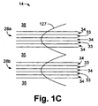
- Fig. 1C is a graphic representation of part of the standing wave pattern 127 and the multiple quantum wells 28a and28b of Fig. 1B.
- Each multiple quantum well 28a and 28b occurs at a peak of standing wave pattern 127.
- Each multiple quantum well 28 includes, for example, a plurality of 80 ⁇ ngstrom ( ⁇ ) quantum wells 34 alternating with a plurality of 80 ⁇ high bandgap material cladding layers 33.
- Each multiple quantum well 28 may be comprised of, for example, five 80 ⁇ quantum well layers 34 alternating with six 80 ⁇ high bandgap cladding layers 33.
- the region between the standing wave pattern peaks is comprised of a thicker (on the order of one thousand ⁇ ) layer 35 of high bandgap material cladding layer.
- the structure shown in VCSELs 10 and 100, in which an undoped active region 14 includes multiple quantum wells 28, has a very high degree of current confinement relative to what can be obtained in, for example, an edge emitting laser. This high degree of current confinement is possible because of the manner in which adjacent quantum well layers 34 are separated by a high bandgap cladding layer 33 and will be described in greater detail with respect to Figs. 3B-3C.
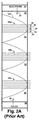
- Fig. 2A is a graphical representation of a conventional vertical injection VCSEL including a periodic gain structure.
- the peaks in standing wave pattern 127 illustrate the regions in which a maximum electric field is present. Therefore, in order to capitalize on this high electric field, the concept of periodic gain places quantum wells at each peak in standing wave pattern 127, and leaves the regions between the peaks, where the electric field is less than at the peaks, devoid of quantum wells.
- multiple quantum well 28a resides at or near the first peak of standing wave pattern 127 to occur after DBR 36. While multiple quantum will 28a will be discussed, the same discussion applies for multiple quantum wells 28b and 28c of Fig. 1B.
- Multiple quantum wells 28a include, for example, a plurality of 80 ⁇ wide quantum wells 34 separated by a plurality of 80 ⁇ wide layers of high bandgap material cladding 33. This structure is repeated in the vicinity of each peak of standing wave pattern 127.
- the electrons traveling perpendicular to the plane of the quantum wells layers travel through doped DBR 36 and, because of their high mobility have little difficulty in traveling to the peaks of standing wave pattern 127.
- holes traveling in the direction indicated by arrow 39 travel through DBR 38, but are much less mobile than electrons. Holes have little difficulty entering the multiple quantum well structure 28c, but because of their lower mobility, holes have difficulty traveling to multiple quantum wells 28b and 28a.
- lateral current injection eliminates the drawback of requiring electrons and holes to traverse the multiple quantum wells, one group after the next, by allowing electrons and holes unimpeded access to the active region.
- Fig. 2B is a graphical representation of the periodic gain structure as applied to the lateral current injection VCSEL constructed in accordance with the invention.
- the n-type material region 11 and p-type material region 12 surround the undoped active region 14 in such a way as to enable holes to travel in the direction indicated by arrow 32, and electrons to travel in the direction indicated by arrow 31 equally into all multiple quantum wells 28a, 28b and 28c.
- the electrons and holes traveling in the direction indicated by arrows 31 and 32, respectively no longer need to pass through the thickness of the cladding layer 35 between the multiple quantum wells 28c and 28b, and 28c to 28a.
- the holes traveling along path 32 can be easily injected from p-type material region 12 into the multiple quantum wells 28a, 28b and 28c in parallel.
- the electrons traveling along path 31 can be easily injected from n-type material region 11 into the multiple quantum wells 28a, 28b and 28c in parallel.
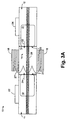
- Fig. 3A is a cross-sectional schematic view of VCSEL 10 of Figs. 1A-1C illustrating the lateral current injection scheme and the material disordering of the invention.
- disordering the n-type and p-type material regions 11 and 12, respectively, to form n-type disordered region 19 and p-type disordered region 21, respectively, adjoining undoped active region 14 improves current confinement in the undoped active region in which a high bandgap material cladding layer 33 is alternately applied with the low bandgap quantum wells layer 34.
- the disordered regions 19 and 21 present a high barrier to electron leakage, particularly at the interface 29 between undoped active region 14 and the disordered p-type material region 21.
- the effect of disordering will be explained in further detail with respect to Fig. 3B.
- the VCSEL structure in accordance with the invention also reduces another type of current leakage that occurs when current flows through the layers 35 of high bandgap material cladding layers separating multiple quantum wells 28a, 28b and 28c.
- the structure of a VCSEL in accordance with the invention which includes high bandgap material cladding layers separating the multiple quantum wells, forces a majority of the current to flow through the low bandgap quantum well material while minimizing the amount of current that flows through the high bandgap barrier cladding layers 35.
- the same structure is used to provide both optical confinement and current confinement.
- the confinement structure is formed of a low band-gap material and an intermediate band-gap material, which compromises the effectiveness of the current confinement.
- the current confinement structure is not also required to provide optical confinement, and so can be formed of low band-gap material multiple quantum wells and high band-gap energy cladding layers. This greatly increases the effectiveness of the current confinement compared with the current confinement obtained in edge-emitting lasers.
- This arrangement results in a lower leakage current than would be possible in an edge-emitting structure in which an intermediate bandgap material cladding layer is necessary to obtain the desired optical mode confinement.
- the intermediate bandgap cladding material that is required in an edge-emitting laser prevents a high bandgap cladding layer from being applied adjacent to the low bandgap quantum well, thus preventing an edge-emitting laser from achieving the level of current confinement achievable by a VCSEL constructed in accordance with the invention.
- a VCSEL constructed in accordance with the invention has significant advantages over an edge-emitting laser. This current confinement will be described in greater detail with reference to Fig. 5.
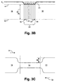
- Fig. 3B is a graphical representation of a vertical band diagram illustrating the effects on current confinement provided by disordered region 21.
- Line bb' represents the minimum energy level in the VCSEL 10 of Fig. 3A, which energy level occurs in undoped active region 14 in the vicinity of each quantum well 34.
- Line cc' represents the energy level present in the VCSEL after disordering the p-type material region 12 and the n-type material region 11.
- disordered region line 41 illustrates an approximation of the drastic change in energy level evident in disordered region 21 after disordering.
- the energy level across the entire multiple quantum well structure 28 is the same irrespective of whether the multiple quantum well 28 resides in p-type material region 12, undoped active region 14, or n-type material region 11.
- disordering the p-type material region 12 drastically improves lateral current confinement of the VCSEL structure 10 by creating a barrier to electron flow at that interface.
- An analogous condition is created at the interface between n-type disordered region 11 and undoped active region 14.
- the structure of VCSELs in general allows a high bandgap cladding layer to be alternately applied with each quantum well in the multiple quantum well structure, without the use of a intermediate bandgap layer as required in edge-emitting lasers.
- This structure enables VCSELs to employ the above described disordering in order to maximize lateral current confinement. This concept will be further illustrated below with respect to Fig. 4.
- Fig. 3C is a lateral band profile of the undoped active region 14 of Fig. 3A illustrating the manner in which disordering creates a double heterostructure.
- the double heterostructure laterally confines electrons and holes within the undoped active region 14.
- Fig. 3B disordering the p-type material region 12 to form disordered region 21 and disordering n-type material 11 to form disordered region 19 adjacent to undoped active region 14, creates an electron and hole barrier height ⁇ B at interface 23 and interface 29 of Fig. 3A.
- This disordering effectively forms the double heterostructure illustrated in Fig. 3C.
- Fig. 4B shows a vertical band diagram comparing the electron barrier height ⁇ B obtained by disordering a low bandgap cladding material versus disordering a high bandgap cladding material.
- the electron and hole barrier height ⁇ B is significantly higher in a lateral current injection VCSEL than would be possible using an edge-emitting laser structure because of the intermediate bandgap cladding material required in an edge-emitting laser.
- the intermediate bandgap cladding material is required in an edge-emitting laser to form an optical waveguide to confine the optical mode of the laser.
- the electron barrier height ⁇ B can be maximized more easily in a VCSEL than in an edge emitting laser by using high bandgap cladding layers alternately applied with quantum well layers as described above.
- Line bb ' 51 is illustrative of the low energy level in undoped active region 14 through the presence of multiple quantum wells 28. Assuming a low bandgap cladding material, or possibly an intermediate bandgap cladding material as typically used in edge emitting lasers, the electron barrier height ⁇ B obtained by disordering the low or intermediate bandgap cladding is illustrated by the electron barrier height ⁇ BL shown with reference to line 58.
- the electron barrier height ⁇ B is lower than when disordering a high bandgap cladding layer.
- section line cc ' 52 represents the highest energy level obtained in the system of Fig. 4 prior to disordering.
- the electron barrier height ⁇ BH as illustrated by line 59 is greater than the electron barrier height ⁇ BL obtained when a low or intermediate bandgap cladding material is disordered.
- the value of electron barrier height ⁇ BH shown with respect to line 59 is significantly greater than the value of electron barrier height ⁇ BL shown by line 58.
- a VCSEL structure allows high bandgap cladding layers 33 to be alternated with quantum wells 34, electron barrier height ⁇ BH can be maximized in VCSELs more easily than in edge emitting lasers, where an intermediate bandgap material must be used in order to create a waveguide to contain the optical mode.
- Fig. 5 is a graphical illustration of the current-voltage curves of the high bandgap cladding material and the low bandgap quantum well material of a VCSEL using lateral current injection in accordance with the invention.
- the active region of the VCSEL is comprised of low bandgap quantum wells 34 alternating with high bandgap cladding material 33.
- the voltage across a VCSEL incorporating each of these materials is plotted along the horizontal axis, while the current flowing through each of the materials is plotted along the vertical axis.
- the curve 74 illustrates the current-voltage characteristics of low bandgap multiple quantum well 34 and curve 76 represents the current-voltage characteristics of high bandgap cladding material 33.
- curve 76 represents the current-voltage characteristics of high bandgap cladding material 33.
- the current represented by line 77 represents the leakage current through the cladding material.
- the turn-on voltage of the high bandgap cladding material is significantly higher than the turn-on voltage of the low bandgap quantum well material, thus enabling a VCSEL constructed in accordance with the invention to permit a low level of leakage current.
- the lateral current injection VCSEL structure permits a high bandgap cladding material to be located adjacent to the low bandgap quantum well material, thus providing superior current confinement over that achieved by implementing a lateral current injection scheme with an edge-emitting laser.
- a lateral current injection scheme in an edge-emitting laser must use an intermediate bandgap cladding material adjacent to the low bandgap quantum well and has a lower turn-on voltage and higher leakage current.
Abstract
Description
- The invention relates generally to semiconductor light emitting devices, and, more particularly, to a vertical cavity surface emitting laser having undoped distributed Bragg reflectors (DBRs) and using lateral current injection and a method for maximizing gain and minimizing optical cavity loss.
- Semiconductor lasers in general, and vertical cavity surface emitting lasers (VCSELs) in particular have been used for quite some time in fields such as optical communications.
- The structure of a typical VCSEL cavity includes an active region that is sandwiched between a pair of distributed Bragg reflectors (DBRs). The active region is the area in which electrons and holes recombine to produce useful laser light. The active region may be constructed of bulk semiconductor material, or may be constructed using multiple quantum wells (MQWs) as known in the art. The DBRs are conductive, therefore, current flows through the DBRs into the active region, where recombination of electrons and holes takes place in the active region, thus producing useful light. In this VCSEL arrangement, one of the DBRs will be slightly less reflective than the other to allow light to exit the device through the less reflective DBR.
- One of the drawbacks of this arrangement is that the DBRs must be doped so that current may pass through them. Doping is the process by which the semiconductor material is made conductive by adding either p-type or n-type impurities (or dopants) to the material. However, doping increases the absorption of light within the DBR due to free carrier absorption in both p and n-type materials. In addition, for p-type material, intervalence band absorption further increases the absorption of light within the DBR. These conditions reduce the amount of light available for output from the device. The efficiency of the laser is dependent upon the output coupling, or the amount of light output, versus the amount of light lost within the laser. Increasing the gain and reducing the internal losses within the laser cavity increases the efficiency of the laser.
- Thus, an unaddressed need exists in the industry for a way of increasing the gain in a laser cavity, while minimizing the material loss within the laser cavity, to improve the efficiency and overall operation of the laser.
- The invention provides a highly efficient VCSEL having low optical loss within the laser cavity. Although not limited to these particular applications, the concepts of the invention are particularly applicable to long wavelength VCSELs.
- In a vertical cavity surface emitting laser (VCSEL) including two distributed Bragg reflectors (DBRs) and an undoped active region therebetween, the VCSEL also including p-type and n-type material adjacent to the undoped active region, the invention can be conceptualized as a method for minimizing optical cavity loss, the method comprising the steps of: forming the DBRs such that they are undoped; and laterally injecting current into the undoped active region.
- In architecture, the invention may be conceptualized as a vertical cavity surface emitting laser (VCSEL), comprising: two undoped distributed Bragg reflectors (DBRs) and an undoped active region therebetween. The VCSEL also includes p-type and n-type material laterally adjacent to the undoped active region, wherein the undoped active region and the p-type and the n-type material adjacent the undoped active region are configured for lateral current injection.
- The invention has numerous advantages, a few which are delineated below merely as examples.
- An advantage of the invention is that it increases the efficiency of a VCSEL.
- Another advantage of the invention is that it allows the implementation of a VCSEL having an undoped active region and undoped DBRs.
- Another advantage of the invention is that it allows a VCSEL to be constructed using undoped DBRs.
- Another advantage of the invention is that it allows the implementation of a periodic gain structure within a VCSEL.
- Another advantage of the invention is that the periodic gain structure allows for an increased number of MQWs resulting in the distribution of heat and stimulated emission over a larger active volume, which reduces the temperature within the laser and reduces thermal effects that limit the power of VCSELs.
- Another advantage of the invention is that increasing the quantity of MQWs in the active region allows the gain of the VCSEL to be increased, which allows the required reflectivity of the DBRs to be lowered. This arrangement relaxes the design constraints of the DBRs, while increasing the optical efficiency of the laser.
- Another advantage of the invention is that a VCSEL according to the invention is simple in design and easily implemented on a mass scale for commercial production.
- Other features and advantages of the invention will become apparent to one with skill in the art upon examination of the following drawings and detailed description. These additional features and advantages are intended to be included herein within the scope of the invention.
- The invention, as defined in the claims, can be better understood with reference to the following drawings. The components within the drawings are not necessarily to scale relative to each other, emphasis instead being placed upon clearly illustrating the principles of the invention.
- Fig. 1A is a cross-sectional schematic view illustrating a vertical cavity surface emitting laser (VCSEL) constructed in accordance with the invention;
- Fig. 1B is a cross-sectional schematic view illustrating an alternative embodiment of the VCSEL of Fig. 1A including a periodic gain structure in the active region;
- Fig. 1C is a graphic representation of the standing wave pattern and the
multiple
quantum wells 28a-28b of Fig. 1B; - Fig. 2A is a graphical representation of a conventional vertical injection VCSEL including a periodic gain structure;
- Fig. 2B is a graphical representation of the periodic gain structure as applied to the VCSEL constructed in accordance with the invention;
- Fig. 3A is a cross-sectional schematic view of
VCSEL 10 of Figs. 1A-1C illustrating the lateral current injection scheme of the invention; - Fig. 3B is a graphical representation of a vertical band diagram illustrating the effects on current confinement provided by the disordered region of Fig. 3A;
- Fig. 3C is a lateral band profile of the undoped
active region 14 of Fig. 3A; and - Fig. 4 is a vertical band diagram comparing the electron barrier height ØB obtained by disordering a low bandgap cladding material versus disordering a high bandgap cladding material.
-
- Turning now to the drawings, Fig. 1A is a cross-sectional schematic view illustrating a vertical cavity surface emitting laser (VCSEL) constructed in accordance with the invention. VCSEL 10 includes n-
type material region 11 and p-type material region 12 surroundingintrinsic material region 13. Theintrinsic material region 13 includes undoped semiconductor material and is also the material in which theactive region 14 of the VCSEL is created. As known in the art, VCSEL 10 is typically constructed by growing layers of semiconductor material over a substrate, such as indium phosphide (InP) or gallium arsenide (GaAs) (not shown), and typically includes a number of material layers. The material layers that compriseVCSEL 10 include all n-type material region 11,intrinsic region 13 and p-type material region 12. The type of doping determines the different regions. For example, n-type material region 11 may be doped via ion implantation or diffusion or other techniques known in the art, resulting in an n-type material. Similarly, p-type material region 12 can be doped in similar fashion, resulting in p-type material. - In accordance with the invention,
intrinsic region 13 remains undoped by masking, or other techniques, to prevent theintrinsic region 13 from having either p or n-type characteristics. - Deposited on
intrinsic region 13 are DBRs 16 and 18. DBRs 16 and 18 are typically constructed using alternating layers of semiconductor material having different refractive indices and are undoped in accordance with the invention. For example, the difference in the refractive indices of the materials comprising the layer pair determines the reflectivity of the layer pair. The thickness of each is λ/4n (or odd multiples thereof), where λ is the in vacuum wavelength of light reflected and n is the refractive index of the material. Note that any odd integer multiple of λ/4n may be used. For example, material thickness of 3λ/4n or 5λ/4n may be used as well. As used herein, the term cavity includes undoped DBRs 16 and 18 and undopedactive region 14. - DBRs 16 and 18 are constructed so that one of the DBRs, in this
case DBR 16, is slightly less reflective thanDBR 18, resulting in the light output indicated in the direction ofarrow 26. Alternatively,DBR 18 may be constructed to be less reflective thanDBR 16, in which case the light output would be in the direction opposite that indicated byarrow 26. - In accordance with an aspect of the invention, DBRs 16 and 18 are also constructed of undoped semiconductor material. Alternatively, there may be some instances where DBRs 16 and 18 could be unintentionally lightly doped because of an effect known as background doping. Background doping occurs when material adjoining the DBRs is doped, and due to the inability to precisely control the doping operation, the DBRs unintentionally become lightly doped. In such instances the lightly doped DBRs still provide significantly less optical cavity loss than conventionally doped DBRs.
-
VCSEL 10 includesmetal contacts type material region 11 and p-type material region 12, respectively, through which an electrical potential applied toVCSEL 10 causes the movement of electrons and holes into undopedactive region 14. - In accordance with another aspect of the invention, and to improve current confinement within the VCSEL, which will be described with reference to Figs. 3A-3C, a portion of n-
type material region 11 and a portion of p-type material region 12 may be disordered in the vicinity of each material regions' interface withintrinsic material region 13. Disordering is a process by which the structure of the material layers comprising the n and p-type regions is altered such that a large difference in bandgap appears where the n-type material region 11 meets theintrinsic material region 13, and where the p-type material region 12 meets theintrinsic material region 13. The concept of disordering, and its applicability to the invention, will be described in detail below. -
VCSEL 10 further includes undopedactive region 14 withinintrinsic material region 13. Undopedactive region 14 is the region in which electrons and holes recombine to produce the light output of theVCSEL 10. Electrons travel in the direction indicated byarrow 31 from n-type material 11 and holes travel in the direction indicated byarrow 32 from p-type region 12, to recombine within undopedactive region 14. - Undoped
active region 14 may include a bulk semiconductor material or may include a multiple quantum well (MQW) structure. Examples of a bulk semiconductor include gallium arsenide, indium gallium arsenide, and induim gallium arsenide phosphide. - In a preferred embodiment,
active region 14 includes multiple quantum wells (MQWs) 28.MQWs 28 are located at a peak of thestanding wave pattern 27. Standingwave pattern 27 is a graphical representation of the electric field that is created within undopedactive region 14 betweenundoped DBR 16 andundoped DBR 18. As illustrated, a peak of standingwave pattern 27 typically occurs at the interface of each DBR and undopedactive region 14. Furthermore, multiple quantum wells are located at another peak of standingwave pattern 27 to capitalize on the high electric field, at the peak. - The
VCSEL structure 10 shown in Fig. 1A illustrates a configuration which allows lateral current injection, i.e., a current flow direction perpendicular to the direction in which light is emitted, and parallel to the layers of semi-conductor material. Lateral current injection results from the movement of electrons and holes laterally from n-type material 11 and p-type material 12, respectively, into undopedactive region 14. Lateral current injection allows the use of undoped DBRs and an undoped active region, thus minimizing internal losses within the lasing cavity. Lateral current injection eliminates the requirement of having doped DBRs because the lateral injection scheme allows electrons and holes to enter the active region without passing through the DBRs. - Fig. 1B is a cross-sectional schematic view illustrating an alternative embodiment of the
VCSEL 10 of Fig. 1A. The alternative embodiment has a periodic gain structure in the active region. Like numbered elements with respect to Fig. 1A will not be described again in detail. -
VCSEL 100 includes undopedactive region 14 with multiplequantum wells 28a-28c configured in a periodic gain structure. In the example shown, the standingwave pattern 127 that occurs inVCSEL 100 has five peaks. The peaks in the standing wave occur due to reflections from the DBRs. The number of peaks is determined by the thickness of the active region. As illustrated with respect to Fig. 1A, a peak occurs at the intersection of undopedactive region 14 andDBR 16 and at the intersection of undopedactive region 14 andDBR 18. However, now there are three peaks in standingwave pattern 127 betweenDBR 16 andDBR 18. At each one of these standing wave peaks, a layer of multiple quantum wells is located. For example, multiplequantum wells wave pattern 127 betweenDBR 16 andDBR 18. This arrangement is referred to as a periodic gain structure, and greatly improves the gain of undopedactive region 14. It should be mentioned that a greater or fewer number of standing wave peaks and associated multiple quantum wells may be constructed. - Fig. 1C is a graphic representation of part of the
standing wave pattern 127 and the multiplequantum wells 28a and28b of Fig. 1B. Each multiplequantum well wave pattern 127. Each multiplequantum well 28 includes, for example, a plurality of 80 Ångstrom (Å)quantum wells 34 alternating with a plurality of 80 Å high bandgap material cladding layers 33. Each multiple quantum well 28 may be comprised of, for example, five 80 Å quantum well layers 34 alternating with six 80 Å high bandgap cladding layers 33. The region between the standing wave pattern peaks is comprised of a thicker (on the order of one thousand Å)layer 35 of high bandgap material cladding layer. - The structure shown in
VCSELs active region 14 includes multiplequantum wells 28, has a very high degree of current confinement relative to what can be obtained in, for example, an edge emitting laser. This high degree of current confinement is possible because of the manner in which adjacent quantum well layers 34 are separated by a highbandgap cladding layer 33 and will be described in greater detail with respect to Figs. 3B-3C. - Fig. 2A is a graphical representation of a conventional vertical injection VCSEL including a periodic gain structure. The peaks in standing
wave pattern 127 illustrate the regions in which a maximum electric field is present. Therefore, in order to capitalize on this high electric field, the concept of periodic gain places quantum wells at each peak in standingwave pattern 127, and leaves the regions between the peaks, where the electric field is less than at the peaks, devoid of quantum wells. As illustrated, multiplequantum well 28a resides at or near the first peak of standingwave pattern 127 to occur afterDBR 36. While multiple quantum will 28a will be discussed, the same discussion applies for multiplequantum wells quantum wells 28a include, for example, a plurality of 80 Å widequantum wells 34 separated by a plurality of 80 Å wide layers of highbandgap material cladding 33. This structure is repeated in the vicinity of each peak of standingwave pattern 127. - To help illustrate the operation of a periodic gain structure in a lateral current injection VCSEL constructed in accordance with the invention, the operation of a periodic gain structure as shown in Fig. 2A in a conventional-vertical injection VCSEL structure, will be described first.
- As shown in Fig. 2A, the electrons traveling perpendicular to the plane of the quantum wells layers, i.e., in the direction indicated by
arrow 37, travel through dopedDBR 36 and, because of their high mobility have little difficulty in traveling to the peaks of standingwave pattern 127. Conversely, holes traveling in the direction indicated byarrow 39 travel throughDBR 38, but are much less mobile than electrons. Holes have little difficulty entering the multiplequantum well structure 28c, but because of their lower mobility, holes have difficulty traveling to multiplequantum wells - Fig. 2B is a graphical representation of the periodic gain structure as applied to the lateral current injection VCSEL constructed in accordance with the invention.
- The elements in Fig. 2B that are the same as those discussed with respect to Fig. 2A are like numbered and will not be discussed again in detail.
- In a VCSEL constructed in accordance with the invention, the n-
type material region 11 and p-type material region 12 surround the undopedactive region 14 in such a way as to enable holes to travel in the direction indicated byarrow 32, and electrons to travel in the direction indicated byarrow 31 equally into all multiplequantum wells arrows cladding layer 35 between the multiplequantum wells path 32 can be easily injected from p-type material region 12 into the multiplequantum wells path 31 can be easily injected from n-type material region 11 into the multiplequantum wells - Fig. 3A is a cross-sectional schematic view of
VCSEL 10 of Figs. 1A-1C illustrating the lateral current injection scheme and the material disordering of the invention. As mentioned above, disordering the n-type and p-type material regions region 19 and p-type disorderedregion 21, respectively, adjoining undopedactive region 14 improves current confinement in the undoped active region in which a high bandgapmaterial cladding layer 33 is alternately applied with the low bandgapquantum wells layer 34. Stated differently, thedisordered regions interface 29 between undopedactive region 14 and the disordered p-type material region 21. The effect of disordering will be explained in further detail with respect to Fig. 3B. - The VCSEL structure in accordance with the invention also reduces another type of current leakage that occurs when current flows through the
layers 35 of high bandgap material cladding layers separating multiplequantum wells - Current confinement using layers of different band-gap materials has previously been used in edge-emitting lasers. However, in edge-emitting lasers, the same structure is used to provide both optical confinement and current confinement. This requires that the confinement structure be formed of a low band-gap material and an intermediate band-gap material, which compromises the effectiveness of the current confinement. In the VCSEL structure according to the invention, the current confinement structure is not also required to provide optical confinement, and so can be formed of low band-gap material multiple quantum wells and high band-gap energy cladding layers. This greatly increases the effectiveness of the current confinement compared with the current confinement obtained in edge-emitting lasers. This arrangement results in a lower leakage current than would be possible in an edge-emitting structure in which an intermediate bandgap material cladding layer is necessary to obtain the desired optical mode confinement. The intermediate bandgap cladding material that is required in an edge-emitting laser prevents a high bandgap cladding layer from being applied adjacent to the low bandgap quantum well, thus preventing an edge-emitting laser from achieving the level of current confinement achievable by a VCSEL constructed in accordance with the invention. In this manner, a VCSEL constructed in accordance with the invention has significant advantages over an edge-emitting laser. This current confinement will be described in greater detail with reference to Fig. 5.
- Fig. 3B is a graphical representation of a vertical band diagram illustrating the effects on current confinement provided by
disordered region 21. Line bb' represents the minimum energy level in theVCSEL 10 of Fig. 3A, which energy level occurs in undopedactive region 14 in the vicinity of eachquantum well 34. Line cc' represents the energy level present in the VCSEL after disordering the p-type material region 12 and the n-type material region 11. - Upon disordering part of p-
type material region 12, the material at theinterface 29 of p-type material 12 and undopedactive region 14 presents a barrier to current flow. The energy level encountered by an electron reaching the interface is drastically altered as illustrated bydisordered region line 41.Disordered region line 41 illustrates an approximation of the drastic change in energy level evident indisordered region 21 after disordering. Before disordering, the energy level across the entire multiplequantum well structure 28 is the same irrespective of whether the multiplequantum well 28 resides in p-type material region 12, undopedactive region 14, or n-type material region 11. On other words, there is nothing to prevent current from flowing in the multiple quantum well 28 through theinterface 23 between n-type material region 11 and undopedactive region 14, and through theinterface 29 between p-type material region 12 and undopedactive region 14. After disordering, the energy differential at the interface betweendisordered region 21 and undoped active region 14 (and theinterface 23 betweendisordered region 19 and undoped active region 14) is represented by the term ØB indicated byline 42. This energy barrier ØB represents the change in energy due to disordering, and effectively indicates that multiplequantum wells 28 no longer exist at the interface ofdisordered region 21 and undopedactive region 14. In this manner, disordering the p-type material region 12 drastically improves lateral current confinement of theVCSEL structure 10 by creating a barrier to electron flow at that interface. An analogous condition is created at the interface between n-type disorderedregion 11 and undopedactive region 14. - As stated above, the structure of VCSELs in general allows a high bandgap cladding layer to be alternately applied with each quantum well in the multiple quantum well structure, without the use of a intermediate bandgap layer as required in edge-emitting lasers. This structure enables VCSELs to employ the above described disordering in order to maximize lateral current confinement. This concept will be further illustrated below with respect to Fig. 4.
- Fig. 3C is a lateral band profile of the undoped
active region 14 of Fig. 3A illustrating the manner in which disordering creates a double heterostructure. The double heterostructure laterally confines electrons and holes within the undopedactive region 14. - As referred to in Fig. 3B, disordering the p-
type material region 12 to form disorderedregion 21 and disordering n-type material 11 to form disorderedregion 19 adjacent to undopedactive region 14, creates an electron and hole barrier height ØB atinterface 23 andinterface 29 of Fig. 3A. This disordering effectively forms the double heterostructure illustrated in Fig. 3C. To further illustrate the improvement in current confinement made possible using a lateral current injection VCSEL constructed in accordance with the invention, over that possible using an edge-emitting laser, Fig. 4B shows a vertical band diagram comparing the electron barrier height ØB obtained by disordering a low bandgap cladding material versus disordering a high bandgap cladding material. The electron and hole barrier height ØB is significantly higher in a lateral current injection VCSEL than would be possible using an edge-emitting laser structure because of the intermediate bandgap cladding material required in an edge-emitting laser. The intermediate bandgap cladding material is required in an edge-emitting laser to form an optical waveguide to confine the optical mode of the laser. - As illustrated in Fig. 4, the electron barrier height ØB can be maximized more easily in a VCSEL than in an edge emitting laser by using high bandgap cladding layers alternately applied with quantum well layers as described above. Line bb' 51 is illustrative of the low energy level in undoped
active region 14 through the presence of multiplequantum wells 28. Assuming a low bandgap cladding material, or possibly an intermediate bandgap cladding material as typically used in edge emitting lasers, the electron barrier height ØB obtained by disordering the low or intermediate bandgap cladding is illustrated by the electron barrier height ØBL shown with reference to line 58. When a low or intermediate bandgap cladding material having an energy depicted byline 56 is disordered, resulting in the energy represented byline 57, the electron barrier height ØB is lower than when disordering a high bandgap cladding layer. To illustrate, section line cc' 52 represents the highest energy level obtained in the system of Fig. 4 prior to disordering. When a high bandgap cladding material is disordered, as illustrated byline 54, the electron barrier height ØBH as illustrated byline 59 is greater than the electron barrier height ØBL obtained when a low or intermediate bandgap cladding material is disordered. As shown, the value of electron barrier height ØBH shown with respect toline 59 is significantly greater than the value of electron barrier height ØBL shown by line 58. - Because a VCSEL structure allows high bandgap cladding layers 33 to be alternated with
quantum wells 34, electron barrier height ØBH can be maximized in VCSELs more easily than in edge emitting lasers, where an intermediate bandgap material must be used in order to create a waveguide to contain the optical mode. - Fig. 5 is a graphical illustration of the current-voltage curves of the high bandgap cladding material and the low bandgap quantum well material of a VCSEL using lateral current injection in accordance with the invention. Referring back to Fig. 1C, the active region of the VCSEL is comprised of low
bandgap quantum wells 34 alternating with highbandgap cladding material 33. Referring now to Fig. 5, the voltage across a VCSEL incorporating each of these materials is plotted along the horizontal axis, while the current flowing through each of the materials is plotted along the vertical axis. Thecurve 74 illustrates the current-voltage characteristics of low bandgap multiple quantum well 34 andcurve 76 represents the current-voltage characteristics of highbandgap cladding material 33. As illustrated, at the bias voltage illustrated byline 72, there is significantly more current, as represented by line 71, flowing through the low bandgap quantum well material than there is current, represented byline 77 flowing through the high bandgap cladding material. - The current represented by
line 77 represents the leakage current through the cladding material. The turn-on voltage of the high bandgap cladding material is significantly higher than the turn-on voltage of the low bandgap quantum well material, thus enabling a VCSEL constructed in accordance with the invention to permit a low level of leakage current. The lateral current injection VCSEL structure permits a high bandgap cladding material to be located adjacent to the low bandgap quantum well material, thus providing superior current confinement over that achieved by implementing a lateral current injection scheme with an edge-emitting laser. A lateral current injection scheme in an edge-emitting laser must use an intermediate bandgap cladding material adjacent to the low bandgap quantum well and has a lower turn-on voltage and higher leakage current. - It will be apparent to those skilled in the art that many modifications and variations may be made to the preferred embodiments of the invention, as set forth above, without departing substantially from the principles of the invention. For example, the VCSEL described can be used in a variety of applications using both undoped and lightly doped DBRs. All such modifications and variations are intended to be included herein within the scope of the invention, as defined in the claims that follow.
Claims (10)
- In a vertical cavity surface emitting laser (VCSEL) (10) including two distributed Bragg reflectors (DBRs) (16, 18) and an undoped active region (14) therebetween, said VCSEL (10) also including p-type (12) and n-type (11) material adjacent to said undoped active region (14), a method for minimizing optical cavity loss, the method comprising the steps of:forming said DBRs (16, 18) such that they are undoped; andlaterally injecting current (31, 32) into said undoped active region (14).
- The method of claim 1, further comprising the step of disordering (19, 21) said p-type (12) and n-type (11) material adjacent to said undoped active region (14).
- The method of claim 1 or 2, wherein said undoped active region (14) includes bulk semiconductor material.
- The method of one of the preceding claims, further comprising the step of disposing a quantum well (34) between two layers of high bandgap cladding material (33) in said undoped active region (14).
- The method of claim 4, further comprising the step of disposing a plurality of high bandgap cladding layers (33) alternating between a plurality of quantum wells (34).
- The method of claim 5, wherein said undoped active region (14) exhibits periodic gain.
- The method of one of the preceding claims, wherein each of said two DBRs (16, 18) are lightly undoped.
- A vertical cavity surface emitting laser (VCSEL) (10), comprising:two undoped distributed Bragg reflectors (DBRs) (16, 18) and an undoped active region (14) therebetween, said VCSEL (10) also including p-type (12) and n-type (11) material laterally adjacent to said undoped active region (14);
wherein said undoped active region (14) and said p-type (12) and said n-type (11) material adjacent said undoped active region (14) are configured for lateral current injection. - The VCSEL (10) of claim 8, further comprising a disordered p-type material (21) and a disordered n-type material (19) adjoining said undoped active region (14).
- The VCSEL (10) of claim 8 or 9, wherein said undoped active region (14) further comprises a quantum well (34) disposed between two layers of high bandgap cladding material (33).
Applications Claiming Priority (2)
| Application Number | Priority Date | Filing Date | Title |
|---|---|---|---|
| US38991999A | 1999-09-03 | 1999-09-03 | |
| US389919 | 1999-09-03 |
Publications (2)
| Publication Number | Publication Date |
|---|---|
| EP1081816A2 true EP1081816A2 (en) | 2001-03-07 |
| EP1081816A3 EP1081816A3 (en) | 2002-04-24 |
Family
ID=23540310
Family Applications (1)
| Application Number | Title | Priority Date | Filing Date |
|---|---|---|---|
| EP00113905A Withdrawn EP1081816A3 (en) | 1999-09-03 | 2000-06-30 | Vertical cavity surface emitting laser (VCSEL) having undoped distributed bragg reflectors and using lateral current injection and method for maximizing gain and minimizing optical cavity loss |
Country Status (2)
| Country | Link |
|---|---|
| EP (1) | EP1081816A3 (en) |
| JP (1) | JP2001094209A (en) |
Cited By (8)
| Publication number | Priority date | Publication date | Assignee | Title |
|---|---|---|---|---|
| WO2003044907A2 (en) * | 2001-11-16 | 2003-05-30 | Fox-Tek | Semiconductor laser with disordered and non-disordered quantum well regions |
| DE10253908A1 (en) * | 2002-09-24 | 2004-04-08 | Osram Opto Semiconductors Gmbh | Radiation emitting semiconducting component has radiation generating active layer between 2 distributed Bragg reflectors forming optical resonator; active layer thickness exceeds resonator wavelength |
| EP1488484A2 (en) * | 2002-03-25 | 2004-12-22 | Optical Communication Products, Inc. | Hybrid vertical cavity laser with buried interface |
| US6879306B2 (en) * | 2002-05-02 | 2005-04-12 | Eastman Kodak Company | Scanned display systems using color laser light sources |
| US7352788B2 (en) | 2005-08-15 | 2008-04-01 | Avago Technologies Ecbu Ip (Singapore) Pte, Ltd. | Nitride semiconductor vertical cavity surface emitting laser |
| WO2011013498A1 (en) * | 2009-07-28 | 2011-02-03 | Canon Kabushiki Kaisha | Surface emitting laser with current constriction layer and multiple active region |
| US9356428B2 (en) | 2012-11-02 | 2016-05-31 | Canon Kabushiki Kaisha | Nitride semiconductor surface emitting laser and method of manufacturing the same |
| EP3171204A1 (en) * | 2015-11-19 | 2017-05-24 | Samsung Electronics Co., Ltd. | Electromagnetic wave reflector and optical device including the same |
Families Citing this family (3)
| Publication number | Priority date | Publication date | Assignee | Title |
|---|---|---|---|---|
| US6836495B2 (en) * | 2003-05-07 | 2004-12-28 | Eastman Kodak Company | Vertical cavity laser including inorganic spacer layers |
| JP5777722B2 (en) * | 2010-10-29 | 2015-09-09 | ヒューレット−パッカード デベロップメント カンパニー エル.ピー.Hewlett‐Packard Development Company, L.P. | Small-mode volume vertical cavity surface emitting laser |
| US10340661B2 (en) | 2017-11-01 | 2019-07-02 | International Business Machines Corporation | Electro-optical device with lateral current injection regions |
Citations (7)
| Publication number | Priority date | Publication date | Assignee | Title |
|---|---|---|---|---|
| US4873696A (en) * | 1988-10-31 | 1989-10-10 | The Regents Of The University Of California | Surface-emitting lasers with periodic gain and a parallel driven nipi structure |
| US5068869A (en) * | 1987-06-19 | 1991-11-26 | Lockheed Missiles & Space Company, Inc. | Surface-emitting laser diode |
| US5563902A (en) * | 1994-08-23 | 1996-10-08 | Samsung Electronics, Co. Ltd. | Semiconductor ridge waveguide laser with lateral current injection |
| US5577064A (en) * | 1994-03-24 | 1996-11-19 | Vixel Corporation | Integration of laser with photodiode for feedback control |
| US5608753A (en) * | 1995-06-29 | 1997-03-04 | Xerox Corporation | Semiconductor devices incorporating p-type and n-type impurity induced layer disordered material |
| JPH10209565A (en) * | 1997-01-27 | 1998-08-07 | Fuji Xerox Co Ltd | Lateral current-injection type surface light-emitting semiconductor laser device, its manufacture, and semiconductor laser array |
| JPH11186653A (en) * | 1997-12-24 | 1999-07-09 | Furukawa Electric Co Ltd:The | Semiconductor laser device and manufacture thereof |
Family Cites Families (3)
| Publication number | Priority date | Publication date | Assignee | Title |
|---|---|---|---|---|
| JPS63141384A (en) * | 1986-12-03 | 1988-06-13 | Mitsubishi Electric Corp | Surface light emitting type semiconductor laser device and manufacture thereof |
| JPH02144983A (en) * | 1988-11-25 | 1990-06-04 | Agency Of Ind Science & Technol | Semiconductor laser device with a plurality of active layers |
| JP3785683B2 (en) * | 1996-07-11 | 2006-06-14 | 大同特殊鋼株式会社 | Surface light emitting device |
-
2000
- 2000-06-30 EP EP00113905A patent/EP1081816A3/en not_active Withdrawn
- 2000-09-04 JP JP2000266531A patent/JP2001094209A/en active Pending
Patent Citations (7)
| Publication number | Priority date | Publication date | Assignee | Title |
|---|---|---|---|---|
| US5068869A (en) * | 1987-06-19 | 1991-11-26 | Lockheed Missiles & Space Company, Inc. | Surface-emitting laser diode |
| US4873696A (en) * | 1988-10-31 | 1989-10-10 | The Regents Of The University Of California | Surface-emitting lasers with periodic gain and a parallel driven nipi structure |
| US5577064A (en) * | 1994-03-24 | 1996-11-19 | Vixel Corporation | Integration of laser with photodiode for feedback control |
| US5563902A (en) * | 1994-08-23 | 1996-10-08 | Samsung Electronics, Co. Ltd. | Semiconductor ridge waveguide laser with lateral current injection |
| US5608753A (en) * | 1995-06-29 | 1997-03-04 | Xerox Corporation | Semiconductor devices incorporating p-type and n-type impurity induced layer disordered material |
| JPH10209565A (en) * | 1997-01-27 | 1998-08-07 | Fuji Xerox Co Ltd | Lateral current-injection type surface light-emitting semiconductor laser device, its manufacture, and semiconductor laser array |
| JPH11186653A (en) * | 1997-12-24 | 1999-07-09 | Furukawa Electric Co Ltd:The | Semiconductor laser device and manufacture thereof |
Non-Patent Citations (3)
| Title |
|---|
| PATENT ABSTRACTS OF JAPAN vol. 1998, no. 13, 30 November 1998 (1998-11-30) -& JP 10 209565 A (FUJI XEROX CO LTD), 7 August 1998 (1998-08-07) * |
| PATENT ABSTRACTS OF JAPAN vol. 1999, no. 12, 29 October 1999 (1999-10-29) -& JP 11 186653 A (FURUKAWA ELECTRIC CO LTD:THE), 9 July 1999 (1999-07-09) * |
| SCHAUS C F: "TRANSVERSE JUNCTION VERTICAL-CAVITY SURFACE-EMITTING LASER" APPLIED PHYSICS LETTERS, AMERICAN INSTITUTE OF PHYSICS. NEW YORK, US, vol. 58, no. 16, 22 April 1991 (1991-04-22), pages 1736-1738, XP000215890 ISSN: 0003-6951 * |
Cited By (13)
| Publication number | Priority date | Publication date | Assignee | Title |
|---|---|---|---|---|
| WO2003044907A3 (en) * | 2001-11-16 | 2004-03-18 | Fox Tek | Semiconductor laser with disordered and non-disordered quantum well regions |
| WO2003044907A2 (en) * | 2001-11-16 | 2003-05-30 | Fox-Tek | Semiconductor laser with disordered and non-disordered quantum well regions |
| EP1488484A2 (en) * | 2002-03-25 | 2004-12-22 | Optical Communication Products, Inc. | Hybrid vertical cavity laser with buried interface |
| EP1488484A4 (en) * | 2002-03-25 | 2005-10-12 | Optical Comm Products Inc | Hybrid vertical cavity laser with buried interface |
| US6879306B2 (en) * | 2002-05-02 | 2005-04-12 | Eastman Kodak Company | Scanned display systems using color laser light sources |
| DE10253908B4 (en) * | 2002-09-24 | 2010-04-22 | Osram Opto Semiconductors Gmbh | Radiation-emitting semiconductor component |
| DE10253908A1 (en) * | 2002-09-24 | 2004-04-08 | Osram Opto Semiconductors Gmbh | Radiation emitting semiconducting component has radiation generating active layer between 2 distributed Bragg reflectors forming optical resonator; active layer thickness exceeds resonator wavelength |
| US7352788B2 (en) | 2005-08-15 | 2008-04-01 | Avago Technologies Ecbu Ip (Singapore) Pte, Ltd. | Nitride semiconductor vertical cavity surface emitting laser |
| WO2011013498A1 (en) * | 2009-07-28 | 2011-02-03 | Canon Kabushiki Kaisha | Surface emitting laser with current constriction layer and multiple active region |
| US8416824B2 (en) | 2009-07-28 | 2013-04-09 | Canon Kabushiki Kaisha | Surface emitting laser with current constriction layer and multiple active regions |
| US9356428B2 (en) | 2012-11-02 | 2016-05-31 | Canon Kabushiki Kaisha | Nitride semiconductor surface emitting laser and method of manufacturing the same |
| EP3171204A1 (en) * | 2015-11-19 | 2017-05-24 | Samsung Electronics Co., Ltd. | Electromagnetic wave reflector and optical device including the same |
| US10277009B2 (en) | 2015-11-19 | 2019-04-30 | Samsung Electronics Co., Ltd. | Electromagnetic wave reflector and optical device including the same |
Also Published As
| Publication number | Publication date |
|---|---|
| JP2001094209A (en) | 2001-04-06 |
| EP1081816A3 (en) | 2002-04-24 |
Similar Documents
| Publication | Publication Date | Title |
|---|---|---|
| US5425043A (en) | Semiconductor laser | |
| US5724376A (en) | Transparent substrate vertical cavity surface emitting lasers fabricated by semiconductor wafer bonding | |
| US6618414B1 (en) | Hybrid vertical cavity laser with buried interface | |
| JP2004146833A (en) | Electrically pumped vertical cavity surface-emitting laser(vcsel) having a plurality of active regions | |
| US7856045B2 (en) | Surface emitting semiconductor component | |
| US20070223549A1 (en) | High-Power Optoelectronic Device with Improved Beam Quality Incorporating A Lateral Mode Filtering Section | |
| US20030103543A1 (en) | Indium phosphide-based vertical-cavity surface-emitting laser | |
| US20090161716A1 (en) | Laser diode | |
| US7602828B2 (en) | Semiconductor laser diode with narrow lateral beam divergence | |
| JP5254045B2 (en) | Semiconductor laser device | |
| US4982408A (en) | Variable oscillation wavelength semiconduction laser device | |
| US6021146A (en) | Vertical cavity surface emitting laser for high power single mode operation and method of fabrication | |
| US7816163B2 (en) | Radiation-emitting semiconductor body for a vertically emitting laser and method for producing same | |
| EP1081816A2 (en) | Vertical cavity surface emitting laser (VCSEL) having undoped distributed bragg reflectors and using lateral current injection and method for maximizing gain and minimizing optical cavity loss | |
| US7095771B2 (en) | Implant damaged oxide insulating region in vertical cavity surface emitting laser | |
| US7778300B2 (en) | Optically pumped semiconductor device | |
| US6961358B2 (en) | Semiconductor laser | |
| JP2940644B2 (en) | Surface light emitting device | |
| US6687276B2 (en) | Surface emitting semiconductor laser | |
| JP3987138B2 (en) | Semiconductor laser element | |
| RU2197048C1 (en) | Injection laser | |
| JP2002111125A (en) | Distributed feedback semiconductor laser | |
| GB2347558A (en) | Array of wafer bonded vertical cavity surface emitting lasers | |
| US20040081214A1 (en) | Narrow lateral waveguide laser | |
| US7551658B2 (en) | Buried ridge waveguide laser diode |
Legal Events
| Date | Code | Title | Description |
|---|---|---|---|
| PUAI | Public reference made under article 153(3) epc to a published international application that has entered the european phase |
Free format text: ORIGINAL CODE: 0009012 |
|
| AK | Designated contracting states |
Kind code of ref document: A2 Designated state(s): AT BE CH CY DE DK ES FI FR GB GR IE IT LI LU MC NL PT SE |
|
| AX | Request for extension of the european patent |
Free format text: AL;LT;LV;MK;RO;SI |
|
| RAP1 | Party data changed (applicant data changed or rights of an application transferred) |
Owner name: AGILENT TECHNOLOGIES INC. |
|
| RAP1 | Party data changed (applicant data changed or rights of an application transferred) |
Owner name: AGILENT TECHNOLOGIES INC. A DELAWARE CORPORATION |
|
| RAP1 | Party data changed (applicant data changed or rights of an application transferred) |
Owner name: AGILENT TECHNOLOGIES, INC. (A DELAWARE CORPORATION |
|
| PUAL | Search report despatched |
Free format text: ORIGINAL CODE: 0009013 |
|
| AK | Designated contracting states |
Kind code of ref document: A3 Designated state(s): AT BE CH CY DE DK ES FI FR GB GR IE IT LI LU MC NL PT SE |
|
| AX | Request for extension of the european patent |
Free format text: AL;LT;LV;MK;RO;SI |
|
| AKX | Designation fees paid | ||
| REG | Reference to a national code |
Ref country code: DE Ref legal event code: 8566 |
|
| STAA | Information on the status of an ep patent application or granted ep patent |
Free format text: STATUS: THE APPLICATION IS DEEMED TO BE WITHDRAWN |
|
| 18D | Application deemed to be withdrawn |
Effective date: 20021025 |