EP1083624A2 - Planar antenna structure - Google Patents
Planar antenna structure Download PDFInfo
- Publication number
- EP1083624A2 EP1083624A2 EP00660142A EP00660142A EP1083624A2 EP 1083624 A2 EP1083624 A2 EP 1083624A2 EP 00660142 A EP00660142 A EP 00660142A EP 00660142 A EP00660142 A EP 00660142A EP 1083624 A2 EP1083624 A2 EP 1083624A2
- Authority
- EP
- European Patent Office
- Prior art keywords
- antenna
- radiating element
- slot
- structure according
- branches
- Prior art date
- Legal status (The legal status is an assumption and is not a legal conclusion. Google has not performed a legal analysis and makes no representation as to the accuracy of the status listed.)
- Granted
Links
Images

Classifications
-
- H—ELECTRICITY
- H01—ELECTRIC ELEMENTS
- H01Q—ANTENNAS, i.e. RADIO AERIALS
- H01Q9/00—Electrically-short antennas having dimensions not more than twice the operating wavelength and consisting of conductive active radiating elements
- H01Q9/04—Resonant antennas
- H01Q9/0407—Substantially flat resonant element parallel to ground plane, e.g. patch antenna
- H01Q9/0421—Substantially flat resonant element parallel to ground plane, e.g. patch antenna with a shorting wall or a shorting pin at one end of the element
-
- H—ELECTRICITY
- H01—ELECTRIC ELEMENTS
- H01Q—ANTENNAS, i.e. RADIO AERIALS
- H01Q1/00—Details of, or arrangements associated with, antennas
- H01Q1/12—Supports; Mounting means
- H01Q1/22—Supports; Mounting means by structural association with other equipment or articles
- H01Q1/24—Supports; Mounting means by structural association with other equipment or articles with receiving set
- H01Q1/241—Supports; Mounting means by structural association with other equipment or articles with receiving set used in mobile communications, e.g. GSM
- H01Q1/242—Supports; Mounting means by structural association with other equipment or articles with receiving set used in mobile communications, e.g. GSM specially adapted for hand-held use
- H01Q1/243—Supports; Mounting means by structural association with other equipment or articles with receiving set used in mobile communications, e.g. GSM specially adapted for hand-held use with built-in antennas
-
- H—ELECTRICITY
- H01—ELECTRIC ELEMENTS
- H01Q—ANTENNAS, i.e. RADIO AERIALS
- H01Q1/00—Details of, or arrangements associated with, antennas
- H01Q1/40—Radiating elements coated with or embedded in protective material
-
- H—ELECTRICITY
- H01—ELECTRIC ELEMENTS
- H01Q—ANTENNAS, i.e. RADIO AERIALS
- H01Q5/00—Arrangements for simultaneous operation of antennas on two or more different wavebands, e.g. dual-band or multi-band arrangements
- H01Q5/30—Arrangements for providing operation on different wavebands
- H01Q5/307—Individual or coupled radiating elements, each element being fed in an unspecified way
- H01Q5/342—Individual or coupled radiating elements, each element being fed in an unspecified way for different propagation modes
- H01Q5/357—Individual or coupled radiating elements, each element being fed in an unspecified way for different propagation modes using a single feed point
Definitions
- the invention relates to an internal planar antenna structure in small-sized radio apparatus such as mobile phones.
- the antenna In portable radio apparatus it is very desirable that the antenna be placed inside the covers of the apparatus, for a protruding antenna is impractical. In modern mobile stations, for example, the internal antenna naturally has to be small in size. This requirement is further emphasized as mobile stations become smaller and smaller. Furthermore, in dual-band antennas the upper operating band at least should be relatively wide, especially if the apparatus in question is meant to function in more than one system utilizing the 1.7-2 GHz band.
- PIFA plane inverted F antenna
- the radiating element in a PIFA may form a continuous plane, producing an antenna of one useful operating band.
- the radiating element may also have a slot in it which divides the element, viewed from the feed point, into two branches so that an antenna of two useful operating bands can be produced.
- the latter structure is more interesting since mobile stations functioning in two systems utilizing different frequency bands have become popular.
- the dual-band structure also provides for a suitable framework for the description of the present invention.
- Fig. 1 shows an example of a prior-art dual-band PIFA.
- the frame 120 of the apparatus in question which is drawn horizontal and which functions as the ground plane of the antenna.
- a planar radiating element 110 which is supported by insulating pieces, such as 105.
- the radiating element 110 is fed at a point F through a hole 103 in the ground plane.
- a slot 115 which starts from the edge of the element and extends to near the feed point F after having made two rectangular bends. The slot divides the radiating element, viewed from the feed point F, into two branches A1 and A2 which have different lengths.
- the longer branch A1 comprises in this example the main part of the edge regions of the radiating element, and its resonance frequency falls on the lower operating band of the antenna.
- the shorter branch A2 comprises the middle region of the radiating element, and its resonance frequency falls on the upper operating band of the antenna.
- element is relatively narrow so that there exists an electromagnetic coupling of considerable magnitude between the branches.
- the electrical length of the branches is greater than the mechanical length. This, in turn, results in the advantage that an antenna functioning in given frequency bands becomes smaller compared to a corresponding antenna without said electromagnetic coupling.
- a disadvantage of the coupling is, however, that the electrical characteristics of the antenna are affected; for example, the bandwidth becomes smaller and the losses become greater.
- the slot in the radiating element is made wider, the electrical characteristics of the antenna will improve, but the antenna has to be made bigger.
- the frequency bands may also be made wider by increasing the distance between the radiating element and ground plane, but this arrangement, too, has the disadvantage of making the antenna bigger.
- the object of the invention is to reduce said disadvantages associated with the prior art.
- the structure according to the invention is characterized by what is expressed in the independent claim 1. Some preferred embodiments of the invention are presented in the other claims.
- the basic idea of the invention is as follows: a layer of dielectric material, the dielectric constant of which is relatively high, is arranged outwards of the plane of the outer surface of the radiating element of a PIFA.
- the layer is located so as to cover at least the areas in which the electric field is the strongest when the antenna resonates.
- the slot of the radiating element is made advantageously so wide that the effect of the coupling between the branches of the element is small.
- the addition of dielectric material has the known effect of shifting down the resonance frequency or frequencies of the antenna so that in order to retain a given resonance frequency the size of the resonating element has to be reduced.
- the addition of dielectric material at advantageous locations has the effect of keeping the impedance of the antenna close to the nominal value over a wider frequency range, which means a greater bandwidth. This is based on directing the stray flux flowing outside the space between the radiating element and ground plane onto a wider route.
- the widening of the slot of the radiating element results in the improvement of the electrical characteristics of the antenna but, on the other hand, it also results in the fact that the antenna has to be made bigger if the resonance frequencies are to be located as desired.
- the antenna By suitably combining addition of dielectric material "on top" of the radiating element and widening of the slot in the element, the antenna can be made smaller and at least as good in its electrical characteristics as a corresponding prior-art antenna. Alternatively, the electrical characteristics of the antenna can be substantially improved without increasing the size of the antenna. In the latter case, the effects on the size of the antenna of the addition of dielectric material and widening of the slot of the radiating element are opposite to each other.
- a structure may be arranged which falls in or outside the intermediate area between said two cases.
- the invention has the advantage that the structure according to it is simple and relatively low in manufacturing costs.
- Fig. 1 was already discussed in connection with the description of the prior art.
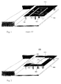
- Fig. 2 shows an example of the antenna structure according to the invention.
- the basic solution in the antenna 200 is identical with that of Fig. 1. It comprises a radiating element 210, ground plane 220, and a short-circuit piece 202 therebetween.
- the inner conductor of the antenna feed line is connected through a hole 203 in the ground plane to the radiating plane 210 at a point F, which in the example depicted is near the front edge of the radiating element.
- the radiating element 210 there is a slot 215 which starts from the left-hand edge of the element as drawn and extends to near the feed point F.
- the slot of the radiating element divides the element, viewed from the feed point F, into two branches A1 and A2. Branch A1 is longer than branch A2.
- the difference from Fig. 1 is that in accordance with the invention the slot is considerably large. It separates the branches Al and A2 to such an extent that the electromagnetic coupling between them is substantially weaker than in the structure of Fig. 1.
- the dielectric plate 230 on the outer surface of the radiating element 210.
- "Outer surface" of the radiating element refers here and in the claims to the surface opposite to that surface of the radiating element which faces the ground plane.
- the dielectric plate 230 is solid and covers portions of the farther ends of branches A1 and A2 as viewed from the feed point F. In these areas the effect of the dielectric material on the stray flux of the antenna is at its greatest because when a branch of the element is in resonance, the electric field is the strongest at the far end of the branch, whereby the stray flux, too, is at its greatest there.
- the dielectric plate 230 additionally covers a great portion of the area 215 between the branches A1 and A2.
- a dielectric layer be here called a superstrate.
- the "superstrate” may be composed of a ceramic or plastic, for example.
- the relative permittivity ⁇ r has to be greater than one; advantageously more than ten.
- the optimum value of the coefficient ⁇ r depends on the case; it may be 40-50, for example.
- Fig. 3 shows the structure according to Fig. 2 viewed from the side and from the higher portion of the frame of the apparatus.
- the ground plane 220 is shown.
- the ends of the branches A1 and A2 are visible as is the space 215 between them, which is shown darker.
- Fig. 3 shows the feed conductor 201, short-circuit piece 202 and one support piece 206 of the radiating element.
- Fig. 4 depicts a few embodiments of the invention.
- the top left subfigure (a) shows the arrangement of Fig. 2 viewed from the ground plane side.
- the superstrate S has a certain permittivity ⁇ .
- Subfigure (b) shows an arrangement which is otherwise identical with that of subfigure (a) but the superstrate now comprises two parts.
- Superstrate Sl covers the end of branch Al of the radiating element, and superstrate S2 covers the end of branch A2.
- subfigure (c) there is shown two superstrates S1 and S2 like in subfigure (b) but with the difference that they have different permittivities ⁇ .
- the permittivity of the former is ⁇ 1 and that of the latter is ⁇ 2 .
- branch A1 is further covered by a third separate superstrate S3 which has a certain permittivity ⁇ 3 .
- Subfigure (d) shows a conventional radiating element with a narrow slot and thereupon, in accordance with the invention, a relatively large superstrate S d .
- the arrangement according to subfigure (d) facilitates antennas of particularly small size.
- Subfigure (e) shows a conventional single-band radiator on top of which, at the opposite end of the element with respect to the feed point F, there is in accordance with the invention a superstratum S e . While such an antenna will not achieve a bandwidth advantage, it will achieve a size advantage.
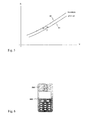
- the curves in Fig. 5 represent in principle a bandwidth B of the antenna as a function of the volume V of the antenna.
- Curve 51 represents the prior art and curve 52 represents the invention. They both are ascending curves, but the curve representing the invention is above the one representing the prior art.
- Indicated in the Figure is a point P corresponding to an antenna according to the prior art.
- the difference indicates the increase ⁇ B in bandwidth.
- the difference indicates the decrease ⁇ V in volume.
- Curves corresponding to those shown in Fig. 5 could also be drawn for the efficiency of the antenna, for example. In that case, too, the curve representing the antenna according to the invention would be above the curve representing the antenna according to the prior art.
- Fig. 6 shows a mobile station 600. It has an antenna 200 according to the invention which in the example depicted is located entirely within the covers of the mobile station.
Abstract
Description
- The invention relates to an internal planar antenna structure in small-sized radio apparatus such as mobile phones.
- In portable radio apparatus it is very desirable that the antenna be placed inside the covers of the apparatus, for a protruding antenna is impractical. In modern mobile stations, for example, the internal antenna naturally has to be small in size. This requirement is further emphasized as mobile stations become smaller and smaller. Furthermore, in dual-band antennas the upper operating band at least should be relatively wide, especially if the apparatus in question is meant to function in more than one system utilizing the 1.7-2 GHz band.
- When aiming at realizing a small-sized antenna the most common solution is to use a PIFA (planar inverted F antenna) structure. The radiating element in a PIFA may form a continuous plane, producing an antenna of one useful operating band. The radiating element may also have a slot in it which divides the element, viewed from the feed point, into two branches so that an antenna of two useful operating bands can be produced. The latter structure is more interesting since mobile stations functioning in two systems utilizing different frequency bands have become popular. The dual-band structure also provides for a suitable framework for the description of the present invention.
- Fig. 1 shows an example of a prior-art dual-band PIFA. In the Figure there can be seen the
frame 120 of the apparatus in question which is drawn horizontal and which functions as the ground plane of the antenna. Above the ground plane there is a planar radiatingelement 110 which is supported by insulating pieces, such as 105. Between the radiating element and ground plane there is a short-circuit piece 102. The radiatingelement 110 is fed at a point F through ahole 103 in the ground plane. In the radiating element there is aslot 115 which starts from the edge of the element and extends to near the feed point F after having made two rectangular bends. The slot divides the radiating element, viewed from the feed point F, into two branches A1 and A2 which have different lengths. The longer branch A1 comprises in this example the main part of the edge regions of the radiating element, and its resonance frequency falls on the lower operating band of the antenna. The shorter branch A2 comprises the middle region of the radiating element, and its resonance frequency falls on the upper operating band of the antenna.
element is relatively narrow so that there exists an electromagnetic coupling of considerable magnitude between the branches. As a consequence, the electrical length of the branches is greater than the mechanical length. This, in turn, results in the advantage that an antenna functioning in given frequency bands becomes smaller compared to a corresponding antenna without said electromagnetic coupling. A disadvantage of the coupling is, however, that the electrical characteristics of the antenna are affected; for example, the bandwidth becomes smaller and the losses become greater. Conversely, if the slot in the radiating element is made wider, the electrical characteristics of the antenna will improve, but the antenna has to be made bigger. As is known, the frequency bands may also be made wider by increasing the distance between the radiating element and ground plane, but this arrangement, too, has the disadvantage of making the antenna bigger. - The object of the invention is to reduce said disadvantages associated with the prior art. The structure according to the invention is characterized by what is expressed in the
independent claim 1. Some preferred embodiments of the invention are presented in the other claims. - The basic idea of the invention is as follows: a layer of dielectric material, the dielectric constant of which is relatively high, is arranged outwards of the plane of the outer surface of the radiating element of a PIFA. The layer is located so as to cover at least the areas in which the electric field is the strongest when the antenna resonates. In the case of a dual-band antenna the slot of the radiating element is made advantageously so wide that the effect of the coupling between the branches of the element is small.
- The addition of dielectric material has the known effect of shifting down the resonance frequency or frequencies of the antenna so that in order to retain a given resonance frequency the size of the resonating element has to be reduced. On the other hand, the addition of dielectric material at advantageous locations has the effect of keeping the impedance of the antenna close to the nominal value over a wider frequency range, which means a greater bandwidth. This is based on directing the stray flux flowing outside the space between the radiating element and ground plane onto a wider route. As was described above, the widening of the slot of the radiating element results in the improvement of the electrical characteristics of the antenna but, on the other hand, it also results in the fact that the antenna has to be made bigger if the resonance frequencies are to be located as desired.
- By suitably combining addition of dielectric material "on top" of the radiating element and widening of the slot in the element, the antenna can be made smaller and at least as good in its electrical characteristics as a corresponding prior-art antenna. Alternatively, the electrical characteristics of the antenna can be substantially improved without increasing the size of the antenna. In the latter case, the effects on the size of the antenna of the addition of dielectric material and widening of the slot of the radiating element are opposite to each other. Naturally, in accordance with the invention, a structure may be arranged which falls in or outside the intermediate area between said two cases. In addition, the invention has the advantage that the structure according to it is simple and relatively low in manufacturing costs.
- The invention will now be described in detail. In the description, reference will be made to the accompanying drawings in which
- Fig. 1
- shows an example of a PIFA according to the prior art,
- Fig. 2
- shows an example of a PIFA according to the invention,
- Fig. 3
- shows a side view of a structure according to Fig. 2,
- Fig. 4
- shows some embodiments of the invention,
- Fig. 5
- shows by means of curves the advantage achieved by the invention, and
- Fig. 6
- shows an example of a mobile station equipped with an antenna according to the invention.
- Fig. 1 was already discussed in connection with the description of the prior art.
- Fig. 2 shows an example of the antenna structure according to the invention. The basic solution in the
antenna 200 is identical with that of Fig. 1. It comprises a radiatingelement 210,ground plane 220, and a short-circuit piece 202 therebetween. The inner conductor of the antenna feed line is connected through ahole 203 in the ground plane to theradiating plane 210 at a point F, which in the example depicted is near the front edge of the radiating element. In theradiating element 210 there is aslot 215 which starts from the left-hand edge of the element as drawn and extends to near the feed point F. As in Fig. 1, the slot of the radiating element divides the element, viewed from the feed point F, into two branches A1 and A2. Branch A1 is longer than branch A2. The difference from Fig. 1 is that in accordance with the invention the slot is considerably large. It separates the branches Al and A2 to such an extent that the electromagnetic coupling between them is substantially weaker than in the structure of Fig. 1. - The most important difference from known structures is the
dielectric plate 230 on the outer surface of theradiating element 210. "Outer surface" of the radiating element refers here and in the claims to the surface opposite to that surface of the radiating element which faces the ground plane. In the example of Fig. 2 thedielectric plate 230 is solid and covers portions of the farther ends of branches A1 and A2 as viewed from the feed point F. In these areas the effect of the dielectric material on the stray flux of the antenna is at its greatest because when a branch of the element is in resonance, the electric field is the strongest at the far end of the branch, whereby the stray flux, too, is at its greatest there. In the example of Fig. 2, thedielectric plate 230 additionally covers a great portion of thearea 215 between the branches A1 and A2. - Let such a dielectric layer be here called a superstrate. The "superstrate" may be composed of a ceramic or plastic, for example. The greater the permittivity of the superstrate, the greater the stray flux-directing effect thereof. Of course, the relative permittivity εr has to be greater than one; advantageously more than ten. However, when the value of the coefficient εr is increased, the losses caused by the superstrate become adversely high at a certain point. The optimum value of the coefficient εr depends on the case; it may be 40-50, for example.
- Fig. 3 shows the structure according to Fig. 2 viewed from the side and from the higher portion of the frame of the apparatus. The
ground plane 220 is shown. Of the radiating element, the ends of the branches A1 and A2 are visible as is thespace 215 between them, which is shown darker. On top of the radiating element there is asuperstrate 230 such that it covers the branches A1 and A2 partly and the mouth portion between them entirely. In addition, Fig. 3 shows thefeed conductor 201, short-circuit piece 202 and onesupport piece 206 of the radiating element. - Fig. 4 depicts a few embodiments of the invention. The top left subfigure (a) shows the arrangement of Fig. 2 viewed from the ground plane side. There is on the outer surface of the radiating element 410 a superstrate S, like the
layer 230 in Figs. 2 and 3. The superstrate S has a certain permittivity ε. Subfigure (b) shows an arrangement which is otherwise identical with that of subfigure (a) but the superstrate now comprises two parts. Superstrate Sl covers the end of branch Al of the radiating element, and superstrate S2 covers the end of branch A2. In subfigure (c) there is shown two superstrates S1 and S2 like in subfigure (b) but with the difference that they have different permittivities ε. The permittivity of the former is ε1 and that of the latter is ε2. In addition, branch A1 is further covered by a third separate superstrate S3 which has a certain permittivity ε3. Subfigure (d) shows a conventional radiating element with a narrow slot and thereupon, in accordance with the invention, a relatively large superstrate Sd. The arrangement according to subfigure (d) facilitates antennas of particularly small size. Subfigure (e) shows a conventional single-band radiator on top of which, at the opposite end of the element with respect to the feed point F, there is in accordance with the invention a superstratum Se. While such an antenna will not achieve a bandwidth advantage, it will achieve a size advantage. - The curves in Fig. 5 represent in principle a bandwidth B of the antenna as a function of the volume V of the antenna.
Curve 51 represents the prior art andcurve 52 represents the invention. They both are ascending curves, but the curve representing the invention is above the one representing the prior art. Indicated in the Figure is a point P corresponding to an antenna according to the prior art. When applying the invention to this antenna, it is possible to move in different directions from the point P. When moving tocurve 52 in the vertical direction, the difference indicates the increase ΔB in bandwidth. When moving tocurve 52 in the horizontal direction, the difference indicates the decrease ΔV in volume. Curves corresponding to those shown in Fig. 5 could also be drawn for the efficiency of the antenna, for example. In that case, too, the curve representing the antenna according to the invention would be above the curve representing the antenna according to the prior art. - Fig. 6 shows a
mobile station 600. It has anantenna 200 according to the invention which in the example depicted is located entirely within the covers of the mobile station. - Above it was described an antenna structure according to the invention and some of its variants. The invention is not limited to them as far as the design of the radiating element and the location of the superstrate are concerned. Furthermore, the invention does not limit other structural solutions of the planar antenna nor its manufacturing method. The inventional idea can be applied in many ways within the scope defined by the
independent claim 1.
Claims (7)
- An antenna structure comprising a planar radiating element and ground plane, characterized in that there is a layer of dielectric material (230) outwards of the plane of the outer surface of the radiating element (210).
- A structure according to claim 1, whereby the radiating element has a slot extending to its edge, said slot dividing the radiating element, viewed from its feed point (F), into two branches (A1, A2) in order to provide two separate operating frequency bands, characterized in that the area of said slot is greater than a tenth of the area of the radiating element.
- A structure according to claim 2, characterized in that said dielectric layer covers at least partly the farthest areas of said branches as viewed from said feed point.
- A structure according to claim 1, characterized in that said dielectric layer comprises at least two separate parts (S1, S2).
- A structure according to claim 4, characterized in that at least two parts that belong to said dielectric layer have different permittivities (ε1, ε2).
- A structure according to claim 1, characterized in that the dielectric constant of said dielectric material is greater than ten.
- A radio apparatus (600) comprising an antenna (200), which includes a radiating plane and ground plane, characterized in that there is a layer of dielectric material outwards of the plane of the outer surface of said radiating element.
Applications Claiming Priority (2)
| Application Number | Priority Date | Filing Date | Title |
|---|---|---|---|
| FI991929A FI114587B (en) | 1999-09-10 | 1999-09-10 | Level Antenna Structure |
| FI991929 | 1999-09-10 |
Publications (3)
| Publication Number | Publication Date |
|---|---|
| EP1083624A2 true EP1083624A2 (en) | 2001-03-14 |
| EP1083624A3 EP1083624A3 (en) | 2003-04-02 |
| EP1083624B1 EP1083624B1 (en) | 2006-02-22 |
Family
ID=8555267
Family Applications (1)
| Application Number | Title | Priority Date | Filing Date |
|---|---|---|---|
| EP00660142A Expired - Lifetime EP1083624B1 (en) | 1999-09-10 | 2000-08-28 | Planar antenna structure |
Country Status (6)
| Country | Link |
|---|---|
| US (1) | US6380905B1 (en) |
| EP (1) | EP1083624B1 (en) |
| CN (1) | CN1188929C (en) |
| AT (1) | ATE318453T1 (en) |
| DE (1) | DE60026132T2 (en) |
| FI (1) | FI114587B (en) |
Cited By (8)
| Publication number | Priority date | Publication date | Assignee | Title |
|---|---|---|---|---|
| US6876320B2 (en) | 2001-11-30 | 2005-04-05 | Fractus, S.A. | Anti-radar space-filling and/or multilevel chaff dispersers |
| EP1753081A1 (en) * | 2005-08-12 | 2007-02-14 | Hirschmann Car Communication GmbH | Planar mobile radio antenna for a vehicle |
| US7245196B1 (en) | 2000-01-19 | 2007-07-17 | Fractus, S.A. | Fractal and space-filling transmission lines, resonators, filters and passive network elements |
| US8738103B2 (en) | 2006-07-18 | 2014-05-27 | Fractus, S.A. | Multiple-body-configuration multimedia and smartphone multifunction wireless devices |
| US9755314B2 (en) | 2001-10-16 | 2017-09-05 | Fractus S.A. | Loaded antenna |
| US9761934B2 (en) | 1999-09-20 | 2017-09-12 | Fractus, S.A. | Multilevel antennae |
| US9905940B2 (en) | 1999-10-26 | 2018-02-27 | Fractus, S.A. | Interlaced multiband antenna arrays |
| US10355346B2 (en) | 2000-01-19 | 2019-07-16 | Fractus, S.A. | Space-filling miniature antennas |
Families Citing this family (62)
| Publication number | Priority date | Publication date | Assignee | Title |
|---|---|---|---|---|
| EP1313166B1 (en) | 2000-04-19 | 2007-11-14 | Advanced Automotive Antennas, S.L. | Multilevel advanced antenna for motor vehicles |
| FI113812B (en) * | 2000-10-27 | 2004-06-15 | Nokia Corp | Radio equipment and antenna structure |
| EP1387433B1 (en) * | 2001-04-23 | 2006-05-31 | Yokowo Co., Ltd | Broad-band antenna for mobile communication |
| FI118403B (en) | 2001-06-01 | 2007-10-31 | Pulse Finland Oy | Dielectric antenna |
| US6552686B2 (en) * | 2001-09-14 | 2003-04-22 | Nokia Corporation | Internal multi-band antenna with improved radiation efficiency |
| US6476769B1 (en) * | 2001-09-19 | 2002-11-05 | Nokia Corporation | Internal multi-band antenna |
| EP1942551A1 (en) | 2001-10-16 | 2008-07-09 | Fractus, S.A. | Multiband antenna |
| FI115343B (en) * | 2001-10-22 | 2005-04-15 | Filtronic Lk Oy | Internal multi-band antenna |
| US6542123B1 (en) * | 2001-10-24 | 2003-04-01 | Auden Techno Corp. | Hidden wideband antenna |
| US8339265B2 (en) | 2002-01-09 | 2012-12-25 | Sensormatic Electronics, Llc. | Method of assigning and deducing the location of articles detected by multiple RFID antennae |
| CN100382390C (en) * | 2002-10-23 | 2008-04-16 | 启碁科技股份有限公司 | Double frequency antenna |
| FI114837B (en) * | 2002-10-24 | 2004-12-31 | Nokia Corp | Radio equipment and antenna structure |
| US7183982B2 (en) * | 2002-11-08 | 2007-02-27 | Centurion Wireless Technologies, Inc. | Optimum Utilization of slot gap in PIFA design |
| CN100495816C (en) * | 2002-11-08 | 2009-06-03 | 圣韵无线技术公司 | Optimum utilization of slot gap in PIFA design |
| US6909402B2 (en) * | 2003-06-11 | 2005-06-21 | Sony Ericsson Mobile Communications Ab | Looped multi-branch planar antennas having multiple resonant frequency bands and wireless terminals incorporating the same |
| US6924770B2 (en) * | 2003-07-25 | 2005-08-02 | Sony Ericsson Mobile Communications Ab | External modular antennas and wireless terminals incorporating the same |
| US7372411B2 (en) * | 2004-06-28 | 2008-05-13 | Nokia Corporation | Antenna arrangement and method for making the same |
| TWI304664B (en) * | 2004-06-30 | 2008-12-21 | Hon Hai Prec Ind Co Ltd | Antenna |
| US7119748B2 (en) * | 2004-12-31 | 2006-10-10 | Nokia Corporation | Internal multi-band antenna with planar strip elements |
| FI20055420A0 (en) * | 2005-07-25 | 2005-07-25 | Lk Products Oy | Adjustable multi-band antenna |
| FI119009B (en) | 2005-10-03 | 2008-06-13 | Pulse Finland Oy | Multiple-band antenna |
| FI118782B (en) | 2005-10-14 | 2008-03-14 | Pulse Finland Oy | Adjustable antenna |
| US8618990B2 (en) | 2011-04-13 | 2013-12-31 | Pulse Finland Oy | Wideband antenna and methods |
| FI20075269A0 (en) | 2007-04-19 | 2007-04-19 | Pulse Finland Oy | Method and arrangement for antenna matching |
| FI120427B (en) | 2007-08-30 | 2009-10-15 | Pulse Finland Oy | Adjustable multiband antenna |
| JP4930359B2 (en) * | 2007-12-18 | 2012-05-16 | ソニー株式会社 | Antenna device |
| TWI466377B (en) * | 2009-01-13 | 2014-12-21 | Realtek Semiconductor Corp | Multi-band printed antenna |
| EP2239813B1 (en) * | 2009-04-09 | 2016-09-14 | Samsung Electronics Co., Ltd. | Internal antenna and portable communication terminal using the same |
| KR101586498B1 (en) * | 2009-04-09 | 2016-01-21 | 삼성전자주식회사 | Internal antenna and portable communication terminal using the same |
| CN101908671B (en) * | 2009-06-05 | 2014-10-08 | 瑞昱半导体股份有限公司 | Multiband printed antenna |
| FI20096134A0 (en) | 2009-11-03 | 2009-11-03 | Pulse Finland Oy | Adjustable antenna |
| FI20096251A0 (en) | 2009-11-27 | 2009-11-27 | Pulse Finland Oy | MIMO antenna |
| US8847833B2 (en) | 2009-12-29 | 2014-09-30 | Pulse Finland Oy | Loop resonator apparatus and methods for enhanced field control |
| FI20105158A (en) | 2010-02-18 | 2011-08-19 | Pulse Finland Oy | SHELL RADIATOR ANTENNA |
| US9406998B2 (en) | 2010-04-21 | 2016-08-02 | Pulse Finland Oy | Distributed multiband antenna and methods |
| CN102340058B (en) * | 2010-07-21 | 2015-11-25 | 神讯电脑(昆山)有限公司 | Antenna structure |
| FI20115072A0 (en) | 2011-01-25 | 2011-01-25 | Pulse Finland Oy | Multi-resonance antenna, antenna module and radio unit |
| US8648752B2 (en) | 2011-02-11 | 2014-02-11 | Pulse Finland Oy | Chassis-excited antenna apparatus and methods |
| US9673507B2 (en) | 2011-02-11 | 2017-06-06 | Pulse Finland Oy | Chassis-excited antenna apparatus and methods |
| US9368879B1 (en) | 2011-05-25 | 2016-06-14 | The Boeing Company | Ultra wide band antenna element |
| US9099777B1 (en) | 2011-05-25 | 2015-08-04 | The Boeing Company | Ultra wide band antenna element |
| US8866689B2 (en) | 2011-07-07 | 2014-10-21 | Pulse Finland Oy | Multi-band antenna and methods for long term evolution wireless system |
| US9450291B2 (en) | 2011-07-25 | 2016-09-20 | Pulse Finland Oy | Multiband slot loop antenna apparatus and methods |
| US9123990B2 (en) | 2011-10-07 | 2015-09-01 | Pulse Finland Oy | Multi-feed antenna apparatus and methods |
| US9531058B2 (en) | 2011-12-20 | 2016-12-27 | Pulse Finland Oy | Loosely-coupled radio antenna apparatus and methods |
| US9484619B2 (en) | 2011-12-21 | 2016-11-01 | Pulse Finland Oy | Switchable diversity antenna apparatus and methods |
| US8988296B2 (en) | 2012-04-04 | 2015-03-24 | Pulse Finland Oy | Compact polarized antenna and methods |
| US9979078B2 (en) | 2012-10-25 | 2018-05-22 | Pulse Finland Oy | Modular cell antenna apparatus and methods |
| US10069209B2 (en) | 2012-11-06 | 2018-09-04 | Pulse Finland Oy | Capacitively coupled antenna apparatus and methods |
| US9172147B1 (en) * | 2013-02-20 | 2015-10-27 | The Boeing Company | Ultra wide band antenna element |
| US9647338B2 (en) | 2013-03-11 | 2017-05-09 | Pulse Finland Oy | Coupled antenna structure and methods |
| US10079428B2 (en) | 2013-03-11 | 2018-09-18 | Pulse Finland Oy | Coupled antenna structure and methods |
| US9634383B2 (en) | 2013-06-26 | 2017-04-25 | Pulse Finland Oy | Galvanically separated non-interacting antenna sector apparatus and methods |
| US9680212B2 (en) | 2013-11-20 | 2017-06-13 | Pulse Finland Oy | Capacitive grounding methods and apparatus for mobile devices |
| US9590308B2 (en) | 2013-12-03 | 2017-03-07 | Pulse Electronics, Inc. | Reduced surface area antenna apparatus and mobile communications devices incorporating the same |
| US9350081B2 (en) | 2014-01-14 | 2016-05-24 | Pulse Finland Oy | Switchable multi-radiator high band antenna apparatus |
| US9973228B2 (en) | 2014-08-26 | 2018-05-15 | Pulse Finland Oy | Antenna apparatus with an integrated proximity sensor and methods |
| US9948002B2 (en) | 2014-08-26 | 2018-04-17 | Pulse Finland Oy | Antenna apparatus with an integrated proximity sensor and methods |
| US9722308B2 (en) | 2014-08-28 | 2017-08-01 | Pulse Finland Oy | Low passive intermodulation distributed antenna system for multiple-input multiple-output systems and methods of use |
| US9906260B2 (en) | 2015-07-30 | 2018-02-27 | Pulse Finland Oy | Sensor-based closed loop antenna swapping apparatus and methods |
| SE539651C2 (en) * | 2016-04-18 | 2017-10-24 | Incoax Networks Europe Ab | A MULTI-BAND WLAN ANTENNA DEVICE |
| USD824885S1 (en) * | 2017-02-25 | 2018-08-07 | Airgain Incorporated | Multiple antennas assembly |
Citations (6)
| Publication number | Priority date | Publication date | Assignee | Title |
|---|---|---|---|---|
| AU5589873A (en) * | 1972-10-05 | 1974-11-21 | Antenna Eng Australia | Low-profile antennas low-profile antennas |
| US5453754A (en) * | 1992-07-02 | 1995-09-26 | The Secretary Of State For Defence In Her Brittanic Majesty's Government Of The United Kingdom Of Great Britain And Northern Ireland | Dielectric resonator antenna with wide bandwidth |
| DE19512003A1 (en) * | 1994-04-01 | 1995-10-05 | France Telecom | Antenna for the transmission and / or reception of electromagnetic signals, in particular ultra-high frequencies, and device which uses such an antenna |
| DE19707535A1 (en) * | 1997-02-25 | 1998-08-27 | Rothe Lutz Dr Ing Habil | Foil emitter |
| US5870057A (en) * | 1994-12-08 | 1999-02-09 | Lucent Technologies Inc. | Small antennas such as microstrip patch antennas |
| WO2000025387A1 (en) * | 1998-10-23 | 2000-05-04 | Gradient Technologies, Llc | A planar antenna including a superstrate lens |
Family Cites Families (5)
| Publication number | Priority date | Publication date | Assignee | Title |
|---|---|---|---|---|
| US4835538A (en) | 1987-01-15 | 1989-05-30 | Ball Corporation | Three resonator parasitically coupled microstrip antenna array element |
| US5170175A (en) * | 1991-08-23 | 1992-12-08 | Motorola, Inc. | Thin film resistive loading for antennas |
| US5448252A (en) * | 1994-03-15 | 1995-09-05 | The United States Of America As Represented By The Secretary Of The Air Force | Wide bandwidth microstrip patch antenna |
| US6114996A (en) * | 1997-03-31 | 2000-09-05 | Qualcomm Incorporated | Increased bandwidth patch antenna |
| KR20000068078A (en) | 1997-06-06 | 2000-11-25 | 비센트 비.인그라시아 | Planar antenna with patch radiators for wide bandwidth and pass band function |
-
1999
- 1999-09-10 FI FI991929A patent/FI114587B/en not_active IP Right Cessation
-
2000
- 2000-08-28 EP EP00660142A patent/EP1083624B1/en not_active Expired - Lifetime
- 2000-08-28 AT AT00660142T patent/ATE318453T1/en not_active IP Right Cessation
- 2000-08-28 DE DE60026132T patent/DE60026132T2/en not_active Expired - Lifetime
- 2000-09-08 US US09/658,008 patent/US6380905B1/en not_active Expired - Fee Related
- 2000-09-11 CN CNB001270265A patent/CN1188929C/en not_active Expired - Fee Related
Patent Citations (6)
| Publication number | Priority date | Publication date | Assignee | Title |
|---|---|---|---|---|
| AU5589873A (en) * | 1972-10-05 | 1974-11-21 | Antenna Eng Australia | Low-profile antennas low-profile antennas |
| US5453754A (en) * | 1992-07-02 | 1995-09-26 | The Secretary Of State For Defence In Her Brittanic Majesty's Government Of The United Kingdom Of Great Britain And Northern Ireland | Dielectric resonator antenna with wide bandwidth |
| DE19512003A1 (en) * | 1994-04-01 | 1995-10-05 | France Telecom | Antenna for the transmission and / or reception of electromagnetic signals, in particular ultra-high frequencies, and device which uses such an antenna |
| US5870057A (en) * | 1994-12-08 | 1999-02-09 | Lucent Technologies Inc. | Small antennas such as microstrip patch antennas |
| DE19707535A1 (en) * | 1997-02-25 | 1998-08-27 | Rothe Lutz Dr Ing Habil | Foil emitter |
| WO2000025387A1 (en) * | 1998-10-23 | 2000-05-04 | Gradient Technologies, Llc | A planar antenna including a superstrate lens |
Non-Patent Citations (2)
| Title |
|---|
| LO T K-C ET AL: "BANDWIDTH ENHANCEMENT OF PIFA LOADED WITH VERY HIGH PERMITTIVITY MATERIAL USING FDTD" IEEE ANTENNAS AND PROPAGATION SOCIETY INTERNATIONAL SYMPOSIUM 1998 DIGEST. ANTENNAS: GATEWAYS TO THE GLOBAL NETWORK. ATLANTA, GA, JUNE 21 - 26, 1998, NEW YORK, NY: IEEE, US, vol. 2, 21 June 1998 (1998-06-21), pages 798-801, XP000888174 ISBN: 0-7803-4479-0 * |
| LUK K M ET AL: "CIRCULAR U-SLOT PATCH WITH DIELECTRIC SUPERSTRATE" ELECTRONICS LETTERS, IEE STEVENAGE, GB, vol. 33, no. 12, 5 June 1997 (1997-06-05), pages 1001-1002, XP000727034 ISSN: 0013-5194 * |
Cited By (15)
| Publication number | Priority date | Publication date | Assignee | Title |
|---|---|---|---|---|
| US10056682B2 (en) | 1999-09-20 | 2018-08-21 | Fractus, S.A. | Multilevel antennae |
| US9761934B2 (en) | 1999-09-20 | 2017-09-12 | Fractus, S.A. | Multilevel antennae |
| US9905940B2 (en) | 1999-10-26 | 2018-02-27 | Fractus, S.A. | Interlaced multiband antenna arrays |
| US10355346B2 (en) | 2000-01-19 | 2019-07-16 | Fractus, S.A. | Space-filling miniature antennas |
| US7538641B2 (en) | 2000-01-19 | 2009-05-26 | Fractus, S.A. | Fractal and space-filling transmission lines, resonators, filters and passive network elements |
| US7245196B1 (en) | 2000-01-19 | 2007-07-17 | Fractus, S.A. | Fractal and space-filling transmission lines, resonators, filters and passive network elements |
| US9755314B2 (en) | 2001-10-16 | 2017-09-05 | Fractus S.A. | Loaded antenna |
| US6876320B2 (en) | 2001-11-30 | 2005-04-05 | Fractus, S.A. | Anti-radar space-filling and/or multilevel chaff dispersers |
| EP1753081A1 (en) * | 2005-08-12 | 2007-02-14 | Hirschmann Car Communication GmbH | Planar mobile radio antenna for a vehicle |
| US8738103B2 (en) | 2006-07-18 | 2014-05-27 | Fractus, S.A. | Multiple-body-configuration multimedia and smartphone multifunction wireless devices |
| US9899727B2 (en) | 2006-07-18 | 2018-02-20 | Fractus, S.A. | Multiple-body-configuration multimedia and smartphone multifunction wireless devices |
| US10644380B2 (en) | 2006-07-18 | 2020-05-05 | Fractus, S.A. | Multiple-body-configuration multimedia and smartphone multifunction wireless devices |
| US11031677B2 (en) | 2006-07-18 | 2021-06-08 | Fractus, S.A. | Multiple-body-configuration multimedia and smartphone multifunction wireless devices |
| US11349200B2 (en) | 2006-07-18 | 2022-05-31 | Fractus, S.A. | Multiple-body-configuration multimedia and smartphone multifunction wireless devices |
| US11735810B2 (en) | 2006-07-18 | 2023-08-22 | Fractus, S.A. | Multiple-body-configuration multimedia and smartphone multifunction wireless devices |
Also Published As
| Publication number | Publication date |
|---|---|
| CN1289157A (en) | 2001-03-28 |
| EP1083624B1 (en) | 2006-02-22 |
| FI114587B (en) | 2004-11-15 |
| EP1083624A3 (en) | 2003-04-02 |
| FI19991929A (en) | 2001-03-10 |
| ATE318453T1 (en) | 2006-03-15 |
| US6380905B1 (en) | 2002-04-30 |
| CN1188929C (en) | 2005-02-09 |
| DE60026132T2 (en) | 2006-10-05 |
| DE60026132D1 (en) | 2006-04-27 |
Similar Documents
| Publication | Publication Date | Title |
|---|---|---|
| US6380905B1 (en) | Planar antenna structure | |
| US6348892B1 (en) | Internal antenna for an apparatus | |
| EP1096602B1 (en) | Planar antenna | |
| EP1761971B1 (en) | Chip antenna | |
| EP2328229B1 (en) | Mobile communication device | |
| CN1214487C (en) | Dual purpose antenna | |
| US6759989B2 (en) | Internal multiband antenna | |
| US6922171B2 (en) | Planar antenna structure | |
| EP1401050B1 (en) | Internal antenna | |
| EP1453140B1 (en) | Multi-band planar antenna | |
| KR100533624B1 (en) | Multi band chip antenna with dual feeding port, and mobile communication apparatus using the same | |
| EP1432072A1 (en) | Antenna for flat radio device | |
| US6963308B2 (en) | Multiband antenna | |
| EP1271691B1 (en) | Dielectric resonator antenna | |
| CN1886863A (en) | Internal multiband antenna | |
| US20060187121A1 (en) | Inverted-F antenna | |
| US20010007445A1 (en) | Method for coupling a signal and an antenna structure | |
| CN101116222A (en) | Internal monopole antenna | |
| KR100616545B1 (en) | Multi-band laminated chip antenna using double coupling feeding | |
| CN103985957B (en) | A kind of broadband multi-band built-in mobile phone antenna | |
| CN104767026B (en) | A kind of small mobile communication device antenna for covering seven frequency ranges | |
| KR20080080066A (en) | Multi-band antenna |
Legal Events
| Date | Code | Title | Description |
|---|---|---|---|
| PUAI | Public reference made under article 153(3) epc to a published international application that has entered the european phase |
Free format text: ORIGINAL CODE: 0009012 |
|
| AK | Designated contracting states |
Kind code of ref document: A2 Designated state(s): AT BE CH CY DE DK ES FI FR GB GR IE IT LI LU MC NL PT SE |
|
| AX | Request for extension of the european patent |
Free format text: AL;LT;LV;MK;RO;SI |
|
| RIC1 | Information provided on ipc code assigned before grant |
Free format text: 7H 01Q 9/04 A, 7H 01Q 1/40 B, 7H 01Q 5/00 B, 7H 01Q 1/24 B, 7H 01Q 21/30 B |
|
| PUAL | Search report despatched |
Free format text: ORIGINAL CODE: 0009013 |
|
| AK | Designated contracting states |
Kind code of ref document: A3 Designated state(s): AT BE CH CY DE DK ES FI FR GB GR IE IT LI LU MC NL PT SE |
|
| AX | Request for extension of the european patent |
Extension state: AL LT LV MK RO SI |
|
| 17P | Request for examination filed |
Effective date: 20030908 |
|
| AKX | Designation fees paid |
Designated state(s): AT BE CH CY DE DK ES FI FR GB GR IE IT LI LU MC NL PT SE |
|
| 17Q | First examination report despatched |
Effective date: 20040615 |
|
| GRAP | Despatch of communication of intention to grant a patent |
Free format text: ORIGINAL CODE: EPIDOSNIGR1 |
|
| RAP1 | Party data changed (applicant data changed or rights of an application transferred) |
Owner name: LK PRODUCTS OY |
|
| GRAS | Grant fee paid |
Free format text: ORIGINAL CODE: EPIDOSNIGR3 |
|
| GRAA | (expected) grant |
Free format text: ORIGINAL CODE: 0009210 |
|
| RIN1 | Information on inventor provided before grant (corrected) |
Inventor name: ANNAMAA, PETTERI Inventor name: MIKKOLA, JYRKI |
|
| AK | Designated contracting states |
Kind code of ref document: B1 Designated state(s): AT BE CH CY DE DK ES FI FR GB GR IE IT LI LU MC NL PT SE |
|
| PG25 | Lapsed in a contracting state [announced via postgrant information from national office to epo] |
Ref country code: IT Free format text: LAPSE BECAUSE OF FAILURE TO SUBMIT A TRANSLATION OF THE DESCRIPTION OR TO PAY THE FEE WITHIN THE PRESCRIBED TIME-LIMIT;WARNING: LAPSES OF ITALIAN PATENTS WITH EFFECTIVE DATE BEFORE 2007 MAY HAVE OCCURRED AT ANY TIME BEFORE 2007. THE CORRECT EFFECTIVE DATE MAY BE DIFFERENT FROM THE ONE RECORDED. Effective date: 20060222 Ref country code: BE Free format text: LAPSE BECAUSE OF FAILURE TO SUBMIT A TRANSLATION OF THE DESCRIPTION OR TO PAY THE FEE WITHIN THE PRESCRIBED TIME-LIMIT Effective date: 20060222 Ref country code: NL Free format text: LAPSE BECAUSE OF FAILURE TO SUBMIT A TRANSLATION OF THE DESCRIPTION OR TO PAY THE FEE WITHIN THE PRESCRIBED TIME-LIMIT Effective date: 20060222 Ref country code: FI Free format text: LAPSE BECAUSE OF FAILURE TO SUBMIT A TRANSLATION OF THE DESCRIPTION OR TO PAY THE FEE WITHIN THE PRESCRIBED TIME-LIMIT Effective date: 20060222 Ref country code: LI Free format text: LAPSE BECAUSE OF FAILURE TO SUBMIT A TRANSLATION OF THE DESCRIPTION OR TO PAY THE FEE WITHIN THE PRESCRIBED TIME-LIMIT Effective date: 20060222 Ref country code: AT Free format text: LAPSE BECAUSE OF FAILURE TO SUBMIT A TRANSLATION OF THE DESCRIPTION OR TO PAY THE FEE WITHIN THE PRESCRIBED TIME-LIMIT Effective date: 20060222 Ref country code: CH Free format text: LAPSE BECAUSE OF FAILURE TO SUBMIT A TRANSLATION OF THE DESCRIPTION OR TO PAY THE FEE WITHIN THE PRESCRIBED TIME-LIMIT Effective date: 20060222 |
|
| REG | Reference to a national code |
Ref country code: GB Ref legal event code: FG4D |
|
| REG | Reference to a national code |
Ref country code: CH Ref legal event code: EP |
|
| REG | Reference to a national code |
Ref country code: IE Ref legal event code: FG4D |
|
| REG | Reference to a national code |
Ref country code: SE Ref legal event code: TRGR |
|
| REF | Corresponds to: |
Ref document number: 60026132 Country of ref document: DE Date of ref document: 20060427 Kind code of ref document: P |
|
| PG25 | Lapsed in a contracting state [announced via postgrant information from national office to epo] |
Ref country code: DK Free format text: LAPSE BECAUSE OF FAILURE TO SUBMIT A TRANSLATION OF THE DESCRIPTION OR TO PAY THE FEE WITHIN THE PRESCRIBED TIME-LIMIT Effective date: 20060522 |
|
| PG25 | Lapsed in a contracting state [announced via postgrant information from national office to epo] |
Ref country code: ES Free format text: LAPSE BECAUSE OF FAILURE TO SUBMIT A TRANSLATION OF THE DESCRIPTION OR TO PAY THE FEE WITHIN THE PRESCRIBED TIME-LIMIT Effective date: 20060602 |
|
| PG25 | Lapsed in a contracting state [announced via postgrant information from national office to epo] |
Ref country code: PT Free format text: LAPSE BECAUSE OF FAILURE TO SUBMIT A TRANSLATION OF THE DESCRIPTION OR TO PAY THE FEE WITHIN THE PRESCRIBED TIME-LIMIT Effective date: 20060724 |
|
| NLV1 | Nl: lapsed or annulled due to failure to fulfill the requirements of art. 29p and 29m of the patents act | ||
| PG25 | Lapsed in a contracting state [announced via postgrant information from national office to epo] |
Ref country code: IE Free format text: LAPSE BECAUSE OF NON-PAYMENT OF DUE FEES Effective date: 20060828 |
|
| PG25 | Lapsed in a contracting state [announced via postgrant information from national office to epo] |
Ref country code: MC Free format text: LAPSE BECAUSE OF NON-PAYMENT OF DUE FEES Effective date: 20060831 |
|
| REG | Reference to a national code |
Ref country code: CH Ref legal event code: PL |
|
| ET | Fr: translation filed | ||
| PLBE | No opposition filed within time limit |
Free format text: ORIGINAL CODE: 0009261 |
|
| STAA | Information on the status of an ep patent application or granted ep patent |
Free format text: STATUS: NO OPPOSITION FILED WITHIN TIME LIMIT |
|
| 26N | No opposition filed |
Effective date: 20061123 |
|
| REG | Reference to a national code |
Ref country code: FR Ref legal event code: CD |
|
| PG25 | Lapsed in a contracting state [announced via postgrant information from national office to epo] |
Ref country code: GR Free format text: LAPSE BECAUSE OF FAILURE TO SUBMIT A TRANSLATION OF THE DESCRIPTION OR TO PAY THE FEE WITHIN THE PRESCRIBED TIME-LIMIT Effective date: 20060523 |
|
| PG25 | Lapsed in a contracting state [announced via postgrant information from national office to epo] |
Ref country code: LU Free format text: LAPSE BECAUSE OF NON-PAYMENT OF DUE FEES Effective date: 20060828 |
|
| PG25 | Lapsed in a contracting state [announced via postgrant information from national office to epo] |
Ref country code: CY Free format text: LAPSE BECAUSE OF FAILURE TO SUBMIT A TRANSLATION OF THE DESCRIPTION OR TO PAY THE FEE WITHIN THE PRESCRIBED TIME-LIMIT Effective date: 20060222 |
|
| PGFP | Annual fee paid to national office [announced via postgrant information from national office to epo] |
Ref country code: DE Payment date: 20100825 Year of fee payment: 11 Ref country code: SE Payment date: 20100812 Year of fee payment: 11 Ref country code: FR Payment date: 20100824 Year of fee payment: 11 |
|
| PGFP | Annual fee paid to national office [announced via postgrant information from national office to epo] |
Ref country code: GB Payment date: 20100825 Year of fee payment: 11 |
|
| REG | Reference to a national code |
Ref country code: SE Ref legal event code: EUG |
|
| GBPC | Gb: european patent ceased through non-payment of renewal fee |
Effective date: 20110828 |
|
| REG | Reference to a national code |
Ref country code: FR Ref legal event code: ST Effective date: 20120430 |
|
| REG | Reference to a national code |
Ref country code: DE Ref legal event code: R119 Ref document number: 60026132 Country of ref document: DE Effective date: 20120301 |
|
| PG25 | Lapsed in a contracting state [announced via postgrant information from national office to epo] |
Ref country code: FR Free format text: LAPSE BECAUSE OF NON-PAYMENT OF DUE FEES Effective date: 20110831 Ref country code: GB Free format text: LAPSE BECAUSE OF NON-PAYMENT OF DUE FEES Effective date: 20110828 |
|
| PG25 | Lapsed in a contracting state [announced via postgrant information from national office to epo] |
Ref country code: SE Free format text: LAPSE BECAUSE OF NON-PAYMENT OF DUE FEES Effective date: 20110829 |
|
| PG25 | Lapsed in a contracting state [announced via postgrant information from national office to epo] |
Ref country code: DE Free format text: LAPSE BECAUSE OF NON-PAYMENT OF DUE FEES Effective date: 20120301 |