EP1087444A2 - El display device and electronic device - Google Patents
El display device and electronic device Download PDFInfo
- Publication number
- EP1087444A2 EP1087444A2 EP00119583A EP00119583A EP1087444A2 EP 1087444 A2 EP1087444 A2 EP 1087444A2 EP 00119583 A EP00119583 A EP 00119583A EP 00119583 A EP00119583 A EP 00119583A EP 1087444 A2 EP1087444 A2 EP 1087444A2
- Authority
- EP
- European Patent Office
- Prior art keywords
- display device
- film
- gamma
- signal
- circuit
- Prior art date
- Legal status (The legal status is an assumption and is not a legal conclusion. Google has not performed a legal analysis and makes no representation as to the accuracy of the status listed.)
- Granted
Links
- 239000000758 substrate Substances 0.000 claims description 40
- 239000011368 organic material Substances 0.000 claims description 10
- 239000010409 thin film Substances 0.000 claims description 8
- 229920000642 polymer Polymers 0.000 claims description 5
- 238000007789 sealing Methods 0.000 claims description 5
- 238000012937 correction Methods 0.000 abstract description 61
- 238000004020 luminiscence type Methods 0.000 abstract description 24
- 239000010408 film Substances 0.000 description 109
- 239000010410 layer Substances 0.000 description 57
- 238000000034 method Methods 0.000 description 30
- 239000012535 impurity Substances 0.000 description 25
- 239000000463 material Substances 0.000 description 25
- 239000011159 matrix material Substances 0.000 description 25
- 238000012545 processing Methods 0.000 description 20
- 238000006243 chemical reaction Methods 0.000 description 13
- 230000004913 activation Effects 0.000 description 10
- 229910021417 amorphous silicon Inorganic materials 0.000 description 10
- 125000004429 atom Chemical group 0.000 description 10
- 229910021419 crystalline silicon Inorganic materials 0.000 description 10
- 238000002425 crystallisation Methods 0.000 description 10
- 229910052581 Si3N4 Inorganic materials 0.000 description 9
- 230000008025 crystallization Effects 0.000 description 9
- BHEPBYXIRTUNPN-UHFFFAOYSA-N hydridophosphorus(.) (triplet) Chemical compound [PH] BHEPBYXIRTUNPN-UHFFFAOYSA-N 0.000 description 9
- 239000011229 interlayer Substances 0.000 description 9
- HQVNEWCFYHHQES-UHFFFAOYSA-N silicon nitride Chemical compound N12[Si]34N5[Si]62N3[Si]51N64 HQVNEWCFYHHQES-UHFFFAOYSA-N 0.000 description 9
- 239000001257 hydrogen Substances 0.000 description 8
- 229910052739 hydrogen Inorganic materials 0.000 description 8
- 230000001360 synchronised effect Effects 0.000 description 8
- -1 tungsten nitride Chemical class 0.000 description 8
- UFHFLCQGNIYNRP-UHFFFAOYSA-N Hydrogen Chemical compound [H][H] UFHFLCQGNIYNRP-UHFFFAOYSA-N 0.000 description 7
- 238000004519 manufacturing process Methods 0.000 description 7
- 238000002161 passivation Methods 0.000 description 7
- 239000004065 semiconductor Substances 0.000 description 7
- 238000010438 heat treatment Methods 0.000 description 6
- 239000010936 titanium Substances 0.000 description 6
- RTAQQCXQSZGOHL-UHFFFAOYSA-N Titanium Chemical compound [Ti] RTAQQCXQSZGOHL-UHFFFAOYSA-N 0.000 description 5
- 238000010586 diagram Methods 0.000 description 5
- 239000002356 single layer Substances 0.000 description 5
- 229910052719 titanium Inorganic materials 0.000 description 5
- XKRFYHLGVUSROY-UHFFFAOYSA-N Argon Chemical compound [Ar] XKRFYHLGVUSROY-UHFFFAOYSA-N 0.000 description 4
- IJGRMHOSHXDMSA-UHFFFAOYSA-N Atomic nitrogen Chemical compound N#N IJGRMHOSHXDMSA-UHFFFAOYSA-N 0.000 description 4
- ZOXJGFHDIHLPTG-UHFFFAOYSA-N Boron Chemical compound [B] ZOXJGFHDIHLPTG-UHFFFAOYSA-N 0.000 description 4
- XUIMIQQOPSSXEZ-UHFFFAOYSA-N Silicon Chemical compound [Si] XUIMIQQOPSSXEZ-UHFFFAOYSA-N 0.000 description 4
- 239000012298 atmosphere Substances 0.000 description 4
- 229910052796 boron Inorganic materials 0.000 description 4
- 238000005984 hydrogenation reaction Methods 0.000 description 4
- 238000002347 injection Methods 0.000 description 4
- 239000007924 injection Substances 0.000 description 4
- 239000005001 laminate film Substances 0.000 description 4
- 239000004973 liquid crystal related substance Substances 0.000 description 4
- 238000005070 sampling Methods 0.000 description 4
- 239000003566 sealing material Substances 0.000 description 4
- 229910052710 silicon Inorganic materials 0.000 description 4
- 239000010703 silicon Substances 0.000 description 4
- 229910052721 tungsten Inorganic materials 0.000 description 4
- 239000010937 tungsten Substances 0.000 description 4
- VYPSYNLAJGMNEJ-UHFFFAOYSA-N Silicium dioxide Chemical compound O=[Si]=O VYPSYNLAJGMNEJ-UHFFFAOYSA-N 0.000 description 3
- 229910052782 aluminium Inorganic materials 0.000 description 3
- XAGFODPZIPBFFR-UHFFFAOYSA-N aluminium Chemical compound [Al] XAGFODPZIPBFFR-UHFFFAOYSA-N 0.000 description 3
- 238000000137 annealing Methods 0.000 description 3
- QVGXLLKOCUKJST-UHFFFAOYSA-N atomic oxygen Chemical compound [O] QVGXLLKOCUKJST-UHFFFAOYSA-N 0.000 description 3
- 230000015572 biosynthetic process Effects 0.000 description 3
- 239000003054 catalyst Substances 0.000 description 3
- 150000001875 compounds Chemical class 0.000 description 3
- 239000007789 gas Substances 0.000 description 3
- 238000003475 lamination Methods 0.000 description 3
- 239000001301 oxygen Substances 0.000 description 3
- 229910052760 oxygen Inorganic materials 0.000 description 3
- 229910021420 polycrystalline silicon Inorganic materials 0.000 description 3
- 230000001105 regulatory effect Effects 0.000 description 3
- 239000011347 resin Substances 0.000 description 3
- 229920005989 resin Polymers 0.000 description 3
- 229910052814 silicon oxide Inorganic materials 0.000 description 3
- 238000004544 sputter deposition Methods 0.000 description 3
- WFKWXMTUELFFGS-UHFFFAOYSA-N tungsten Chemical compound [W] WFKWXMTUELFFGS-UHFFFAOYSA-N 0.000 description 3
- KLCLIOISYBHYDZ-UHFFFAOYSA-N 1,4,4-triphenylbuta-1,3-dienylbenzene Chemical compound C=1C=CC=CC=1C(C=1C=CC=CC=1)=CC=C(C=1C=CC=CC=1)C1=CC=CC=C1 KLCLIOISYBHYDZ-UHFFFAOYSA-N 0.000 description 2
- OKTJSMMVPCPJKN-UHFFFAOYSA-N Carbon Chemical compound [C] OKTJSMMVPCPJKN-UHFFFAOYSA-N 0.000 description 2
- 206010010144 Completed suicide Diseases 0.000 description 2
- PXHVJJICTQNCMI-UHFFFAOYSA-N Nickel Chemical compound [Ni] PXHVJJICTQNCMI-UHFFFAOYSA-N 0.000 description 2
- XYFCBTPGUUZFHI-UHFFFAOYSA-N Phosphine Chemical compound P XYFCBTPGUUZFHI-UHFFFAOYSA-N 0.000 description 2
- XLOMVQKBTHCTTD-UHFFFAOYSA-N Zinc monoxide Chemical compound [Zn]=O XLOMVQKBTHCTTD-UHFFFAOYSA-N 0.000 description 2
- 229910052786 argon Inorganic materials 0.000 description 2
- QVQLCTNNEUAWMS-UHFFFAOYSA-N barium oxide Chemical compound [Ba]=O QVQLCTNNEUAWMS-UHFFFAOYSA-N 0.000 description 2
- UMIVXZPTRXBADB-UHFFFAOYSA-N benzocyclobutene Chemical compound C1=CC=C2CCC2=C1 UMIVXZPTRXBADB-UHFFFAOYSA-N 0.000 description 2
- 230000000903 blocking effect Effects 0.000 description 2
- 229910052799 carbon Inorganic materials 0.000 description 2
- 239000011651 chromium Substances 0.000 description 2
- 239000010949 copper Substances 0.000 description 2
- 230000006866 deterioration Effects 0.000 description 2
- 238000001704 evaporation Methods 0.000 description 2
- 230000006870 function Effects 0.000 description 2
- 239000011521 glass Substances 0.000 description 2
- 239000011261 inert gas Substances 0.000 description 2
- 150000002500 ions Chemical class 0.000 description 2
- 238000005224 laser annealing Methods 0.000 description 2
- PQXKHYXIUOZZFA-UHFFFAOYSA-M lithium fluoride Chemical compound [Li+].[F-] PQXKHYXIUOZZFA-UHFFFAOYSA-M 0.000 description 2
- 229910052757 nitrogen Inorganic materials 0.000 description 2
- 230000010355 oscillation Effects 0.000 description 2
- 238000000059 patterning Methods 0.000 description 2
- 230000000737 periodic effect Effects 0.000 description 2
- 229920003227 poly(N-vinyl carbazole) Polymers 0.000 description 2
- 229920000553 poly(phenylenevinylene) Polymers 0.000 description 2
- 229920002098 polyfluorene Polymers 0.000 description 2
- 229920005591 polysilicon Polymers 0.000 description 2
- 238000002360 preparation method Methods 0.000 description 2
- 238000000926 separation method Methods 0.000 description 2
- YLYPIBBGWLKELC-RMKNXTFCSA-N 2-[2-[(e)-2-[4-(dimethylamino)phenyl]ethenyl]-6-methylpyran-4-ylidene]propanedinitrile Chemical compound C1=CC(N(C)C)=CC=C1\C=C\C1=CC(=C(C#N)C#N)C=C(C)O1 YLYPIBBGWLKELC-RMKNXTFCSA-N 0.000 description 1
- 229910000838 Al alloy Inorganic materials 0.000 description 1
- VYZAMTAEIAYCRO-UHFFFAOYSA-N Chromium Chemical compound [Cr] VYZAMTAEIAYCRO-UHFFFAOYSA-N 0.000 description 1
- RYGMFSIKBFXOCR-UHFFFAOYSA-N Copper Chemical compound [Cu] RYGMFSIKBFXOCR-UHFFFAOYSA-N 0.000 description 1
- ZOKXTWBITQBERF-UHFFFAOYSA-N Molybdenum Chemical compound [Mo] ZOKXTWBITQBERF-UHFFFAOYSA-N 0.000 description 1
- 239000004952 Polyamide Substances 0.000 description 1
- 239000004642 Polyimide Substances 0.000 description 1
- 229910001362 Ta alloys Inorganic materials 0.000 description 1
- NRTOMJZYCJJWKI-UHFFFAOYSA-N Titanium nitride Chemical compound [Ti]#N NRTOMJZYCJJWKI-UHFFFAOYSA-N 0.000 description 1
- 229910001080 W alloy Inorganic materials 0.000 description 1
- LEVVHYCKPQWKOP-UHFFFAOYSA-N [Si].[Ge] Chemical compound [Si].[Ge] LEVVHYCKPQWKOP-UHFFFAOYSA-N 0.000 description 1
- NIXOWILDQLNWCW-UHFFFAOYSA-N acrylic acid group Chemical group C(C=C)(=O)O NIXOWILDQLNWCW-UHFFFAOYSA-N 0.000 description 1
- 230000003213 activating effect Effects 0.000 description 1
- 239000000853 adhesive Substances 0.000 description 1
- 230000001070 adhesive effect Effects 0.000 description 1
- 229910045601 alloy Inorganic materials 0.000 description 1
- 239000000956 alloy Substances 0.000 description 1
- 229910052785 arsenic Inorganic materials 0.000 description 1
- RQNWIZPPADIBDY-UHFFFAOYSA-N arsenic atom Chemical compound [As] RQNWIZPPADIBDY-UHFFFAOYSA-N 0.000 description 1
- IVHJCRXBQPGLOV-UHFFFAOYSA-N azanylidynetungsten Chemical compound [W]#N IVHJCRXBQPGLOV-UHFFFAOYSA-N 0.000 description 1
- 239000004305 biphenyl Substances 0.000 description 1
- 229910052804 chromium Inorganic materials 0.000 description 1
- 230000001276 controlling effect Effects 0.000 description 1
- 229910052802 copper Inorganic materials 0.000 description 1
- VBVAVBCYMYWNOU-UHFFFAOYSA-N coumarin 6 Chemical compound C1=CC=C2SC(C3=CC4=CC=C(C=C4OC3=O)N(CC)CC)=NC2=C1 VBVAVBCYMYWNOU-UHFFFAOYSA-N 0.000 description 1
- 238000000151 deposition Methods 0.000 description 1
- 239000002274 desiccant Substances 0.000 description 1
- 238000011161 development Methods 0.000 description 1
- ZOCHARZZJNPSEU-UHFFFAOYSA-N diboron Chemical compound B#B ZOCHARZZJNPSEU-UHFFFAOYSA-N 0.000 description 1
- YMWUJEATGCHHMB-UHFFFAOYSA-N dichloromethane Substances ClCCl YMWUJEATGCHHMB-UHFFFAOYSA-N 0.000 description 1
- 230000000694 effects Effects 0.000 description 1
- 230000005685 electric field effect Effects 0.000 description 1
- 238000005485 electric heating Methods 0.000 description 1
- 238000005401 electroluminescence Methods 0.000 description 1
- 239000000284 extract Substances 0.000 description 1
- 230000017525 heat dissipation Effects 0.000 description 1
- 239000001307 helium Substances 0.000 description 1
- 229910052734 helium Inorganic materials 0.000 description 1
- SWQJXJOGLNCZEY-UHFFFAOYSA-N helium atom Chemical compound [He] SWQJXJOGLNCZEY-UHFFFAOYSA-N 0.000 description 1
- 230000005525 hole transport Effects 0.000 description 1
- 150000002431 hydrogen Chemical class 0.000 description 1
- 229910003437 indium oxide Inorganic materials 0.000 description 1
- PJXISJQVUVHSOJ-UHFFFAOYSA-N indium(iii) oxide Chemical compound [O-2].[O-2].[O-2].[In+3].[In+3] PJXISJQVUVHSOJ-UHFFFAOYSA-N 0.000 description 1
- 230000010354 integration Effects 0.000 description 1
- 238000005468 ion implantation Methods 0.000 description 1
- 238000005499 laser crystallization Methods 0.000 description 1
- 239000002075 main ingredient Substances 0.000 description 1
- 229910052751 metal Inorganic materials 0.000 description 1
- 239000002184 metal Substances 0.000 description 1
- 229910052750 molybdenum Inorganic materials 0.000 description 1
- 239000011733 molybdenum Substances 0.000 description 1
- 229910052759 nickel Inorganic materials 0.000 description 1
- VOFUROIFQGPCGE-UHFFFAOYSA-N nile red Chemical compound C1=CC=C2C3=NC4=CC=C(N(CC)CC)C=C4OC3=CC(=O)C2=C1 VOFUROIFQGPCGE-UHFFFAOYSA-N 0.000 description 1
- 150000004767 nitrides Chemical class 0.000 description 1
- 239000012299 nitrogen atmosphere Substances 0.000 description 1
- 230000003287 optical effect Effects 0.000 description 1
- 239000000049 pigment Substances 0.000 description 1
- 238000005268 plasma chemical vapour deposition Methods 0.000 description 1
- 229910052696 pnictogen Inorganic materials 0.000 description 1
- 229920002647 polyamide Polymers 0.000 description 1
- 229920001721 polyimide Polymers 0.000 description 1
- 230000001737 promoting effect Effects 0.000 description 1
- 238000005215 recombination Methods 0.000 description 1
- 230000006798 recombination Effects 0.000 description 1
- 238000011160 research Methods 0.000 description 1
- 238000012827 research and development Methods 0.000 description 1
- 238000009751 slip forming Methods 0.000 description 1
- 238000004528 spin coating Methods 0.000 description 1
- 229910052715 tantalum Inorganic materials 0.000 description 1
- GUVRBAGPIYLISA-UHFFFAOYSA-N tantalum atom Chemical compound [Ta] GUVRBAGPIYLISA-UHFFFAOYSA-N 0.000 description 1
- MZLGASXMSKOWSE-UHFFFAOYSA-N tantalum nitride Chemical compound [Ta]#N MZLGASXMSKOWSE-UHFFFAOYSA-N 0.000 description 1
- 229910021341 titanium silicide Inorganic materials 0.000 description 1
- 239000011787 zinc oxide Substances 0.000 description 1
Images


Classifications
-
- G—PHYSICS
- G09—EDUCATION; CRYPTOGRAPHY; DISPLAY; ADVERTISING; SEALS
- G09G—ARRANGEMENTS OR CIRCUITS FOR CONTROL OF INDICATING DEVICES USING STATIC MEANS TO PRESENT VARIABLE INFORMATION
- G09G3/00—Control arrangements or circuits, of interest only in connection with visual indicators other than cathode-ray tubes
- G09G3/20—Control arrangements or circuits, of interest only in connection with visual indicators other than cathode-ray tubes for presentation of an assembly of a number of characters, e.g. a page, by composing the assembly by combination of individual elements arranged in a matrix no fixed position being assigned to or needed to be assigned to the individual characters or partial characters
- G09G3/22—Control arrangements or circuits, of interest only in connection with visual indicators other than cathode-ray tubes for presentation of an assembly of a number of characters, e.g. a page, by composing the assembly by combination of individual elements arranged in a matrix no fixed position being assigned to or needed to be assigned to the individual characters or partial characters using controlled light sources
- G09G3/30—Control arrangements or circuits, of interest only in connection with visual indicators other than cathode-ray tubes for presentation of an assembly of a number of characters, e.g. a page, by composing the assembly by combination of individual elements arranged in a matrix no fixed position being assigned to or needed to be assigned to the individual characters or partial characters using controlled light sources using electroluminescent panels
- G09G3/32—Control arrangements or circuits, of interest only in connection with visual indicators other than cathode-ray tubes for presentation of an assembly of a number of characters, e.g. a page, by composing the assembly by combination of individual elements arranged in a matrix no fixed position being assigned to or needed to be assigned to the individual characters or partial characters using controlled light sources using electroluminescent panels semiconductive, e.g. using light-emitting diodes [LED]
- G09G3/3208—Control arrangements or circuits, of interest only in connection with visual indicators other than cathode-ray tubes for presentation of an assembly of a number of characters, e.g. a page, by composing the assembly by combination of individual elements arranged in a matrix no fixed position being assigned to or needed to be assigned to the individual characters or partial characters using controlled light sources using electroluminescent panels semiconductive, e.g. using light-emitting diodes [LED] organic, e.g. using organic light-emitting diodes [OLED]
- G09G3/3225—Control arrangements or circuits, of interest only in connection with visual indicators other than cathode-ray tubes for presentation of an assembly of a number of characters, e.g. a page, by composing the assembly by combination of individual elements arranged in a matrix no fixed position being assigned to or needed to be assigned to the individual characters or partial characters using controlled light sources using electroluminescent panels semiconductive, e.g. using light-emitting diodes [LED] organic, e.g. using organic light-emitting diodes [OLED] using an active matrix
- G09G3/3233—Control arrangements or circuits, of interest only in connection with visual indicators other than cathode-ray tubes for presentation of an assembly of a number of characters, e.g. a page, by composing the assembly by combination of individual elements arranged in a matrix no fixed position being assigned to or needed to be assigned to the individual characters or partial characters using controlled light sources using electroluminescent panels semiconductive, e.g. using light-emitting diodes [LED] organic, e.g. using organic light-emitting diodes [OLED] using an active matrix with pixel circuitry controlling the current through the light-emitting element
-
- H—ELECTRICITY
- H01—ELECTRIC ELEMENTS
- H01L—SEMICONDUCTOR DEVICES NOT COVERED BY CLASS H10
- H01L31/00—Semiconductor devices sensitive to infrared radiation, light, electromagnetic radiation of shorter wavelength or corpuscular radiation and specially adapted either for the conversion of the energy of such radiation into electrical energy or for the control of electrical energy by such radiation; Processes or apparatus specially adapted for the manufacture or treatment thereof or of parts thereof; Details thereof
- H01L31/12—Semiconductor devices sensitive to infrared radiation, light, electromagnetic radiation of shorter wavelength or corpuscular radiation and specially adapted either for the conversion of the energy of such radiation into electrical energy or for the control of electrical energy by such radiation; Processes or apparatus specially adapted for the manufacture or treatment thereof or of parts thereof; Details thereof structurally associated with, e.g. formed in or on a common substrate with, one or more electric light sources, e.g. electroluminescent light sources, and electrically or optically coupled thereto
-
- H—ELECTRICITY
- H10—SEMICONDUCTOR DEVICES; ELECTRIC SOLID-STATE DEVICES NOT OTHERWISE PROVIDED FOR
- H10K—ORGANIC ELECTRIC SOLID-STATE DEVICES
- H10K59/00—Integrated devices, or assemblies of multiple devices, comprising at least one organic light-emitting element covered by group H10K50/00
- H10K59/30—Devices specially adapted for multicolour light emission
- H10K59/35—Devices specially adapted for multicolour light emission comprising red-green-blue [RGB] subpixels
-
- H—ELECTRICITY
- H10—SEMICONDUCTOR DEVICES; ELECTRIC SOLID-STATE DEVICES NOT OTHERWISE PROVIDED FOR
- H10K—ORGANIC ELECTRIC SOLID-STATE DEVICES
- H10K59/00—Integrated devices, or assemblies of multiple devices, comprising at least one organic light-emitting element covered by group H10K50/00
- H10K59/30—Devices specially adapted for multicolour light emission
- H10K59/38—Devices specially adapted for multicolour light emission comprising colour filters or colour changing media [CCM]
-
- G—PHYSICS
- G09—EDUCATION; CRYPTOGRAPHY; DISPLAY; ADVERTISING; SEALS
- G09G—ARRANGEMENTS OR CIRCUITS FOR CONTROL OF INDICATING DEVICES USING STATIC MEANS TO PRESENT VARIABLE INFORMATION
- G09G2300/00—Aspects of the constitution of display devices
- G09G2300/08—Active matrix structure, i.e. with use of active elements, inclusive of non-linear two terminal elements, in the pixels together with light emitting or modulating elements
- G09G2300/0809—Several active elements per pixel in active matrix panels
- G09G2300/0842—Several active elements per pixel in active matrix panels forming a memory circuit, e.g. a dynamic memory with one capacitor
-
- G—PHYSICS
- G09—EDUCATION; CRYPTOGRAPHY; DISPLAY; ADVERTISING; SEALS
- G09G—ARRANGEMENTS OR CIRCUITS FOR CONTROL OF INDICATING DEVICES USING STATIC MEANS TO PRESENT VARIABLE INFORMATION
- G09G2320/00—Control of display operating conditions
- G09G2320/02—Improving the quality of display appearance
- G09G2320/0233—Improving the luminance or brightness uniformity across the screen
-
- G—PHYSICS
- G09—EDUCATION; CRYPTOGRAPHY; DISPLAY; ADVERTISING; SEALS
- G09G—ARRANGEMENTS OR CIRCUITS FOR CONTROL OF INDICATING DEVICES USING STATIC MEANS TO PRESENT VARIABLE INFORMATION
- G09G2320/00—Control of display operating conditions
- G09G2320/02—Improving the quality of display appearance
- G09G2320/0242—Compensation of deficiencies in the appearance of colours
-
- G—PHYSICS
- G09—EDUCATION; CRYPTOGRAPHY; DISPLAY; ADVERTISING; SEALS
- G09G—ARRANGEMENTS OR CIRCUITS FOR CONTROL OF INDICATING DEVICES USING STATIC MEANS TO PRESENT VARIABLE INFORMATION
- G09G2320/00—Control of display operating conditions
- G09G2320/02—Improving the quality of display appearance
- G09G2320/0271—Adjustment of the gradation levels within the range of the gradation scale, e.g. by redistribution or clipping
- G09G2320/0276—Adjustment of the gradation levels within the range of the gradation scale, e.g. by redistribution or clipping for the purpose of adaptation to the characteristics of a display device, i.e. gamma correction
-
- G—PHYSICS
- G09—EDUCATION; CRYPTOGRAPHY; DISPLAY; ADVERTISING; SEALS
- G09G—ARRANGEMENTS OR CIRCUITS FOR CONTROL OF INDICATING DEVICES USING STATIC MEANS TO PRESENT VARIABLE INFORMATION
- G09G2320/00—Control of display operating conditions
- G09G2320/02—Improving the quality of display appearance
- G09G2320/029—Improving the quality of display appearance by monitoring one or more pixels in the display panel, e.g. by monitoring a fixed reference pixel
-
- G—PHYSICS
- G09—EDUCATION; CRYPTOGRAPHY; DISPLAY; ADVERTISING; SEALS
- G09G—ARRANGEMENTS OR CIRCUITS FOR CONTROL OF INDICATING DEVICES USING STATIC MEANS TO PRESENT VARIABLE INFORMATION
- G09G2320/00—Control of display operating conditions
- G09G2320/04—Maintaining the quality of display appearance
- G09G2320/043—Preventing or counteracting the effects of ageing
-
- H—ELECTRICITY
- H01—ELECTRIC ELEMENTS
- H01L—SEMICONDUCTOR DEVICES NOT COVERED BY CLASS H10
- H01L27/00—Devices consisting of a plurality of semiconductor or other solid-state components formed in or on a common substrate
- H01L27/02—Devices consisting of a plurality of semiconductor or other solid-state components formed in or on a common substrate including semiconductor components specially adapted for rectifying, oscillating, amplifying or switching and having at least one potential-jump barrier or surface barrier; including integrated passive circuit elements with at least one potential-jump barrier or surface barrier
- H01L27/12—Devices consisting of a plurality of semiconductor or other solid-state components formed in or on a common substrate including semiconductor components specially adapted for rectifying, oscillating, amplifying or switching and having at least one potential-jump barrier or surface barrier; including integrated passive circuit elements with at least one potential-jump barrier or surface barrier the substrate being other than a semiconductor body, e.g. an insulating body
- H01L27/1214—Devices consisting of a plurality of semiconductor or other solid-state components formed in or on a common substrate including semiconductor components specially adapted for rectifying, oscillating, amplifying or switching and having at least one potential-jump barrier or surface barrier; including integrated passive circuit elements with at least one potential-jump barrier or surface barrier the substrate being other than a semiconductor body, e.g. an insulating body comprising a plurality of TFTs formed on a non-semiconducting substrate, e.g. driving circuits for AMLCDs
-
- H—ELECTRICITY
- H10—SEMICONDUCTOR DEVICES; ELECTRIC SOLID-STATE DEVICES NOT OTHERWISE PROVIDED FOR
- H10K—ORGANIC ELECTRIC SOLID-STATE DEVICES
- H10K59/00—Integrated devices, or assemblies of multiple devices, comprising at least one organic light-emitting element covered by group H10K50/00
- H10K59/10—OLED displays
- H10K59/12—Active-matrix OLED [AMOLED] displays
Definitions
- the present invention is related to an EL (electroluminescence) display device formed by a semiconductor element (an element using a semiconductor thin film, typically a thin-film transistor) built on a substrate, and to an electronic device having the EL display device as a display portion.
- a semiconductor element an element using a semiconductor thin film, typically a thin-film transistor
- a TFT thin-film transistor
- a substrate a thin-film transistor
- a TFT using a polysilicon film has a higher electric field effect mobility than a TFT using a conventional amorphous silicon film, and therefore it is capable of high speed operation. It therefore becomes possible to perform control of a pixel, conventionally performed by a driver circuit external to the substrate, by a driver circuit formed on the same substrate as the pixel.
- This type of active matrix display device is gaining attention for obtaining many advantages, such as lowered manufacturing cost, smaller display device, increased yield, and reduced throughput, by building various circuits and elements on the same substrate.
- the EL display device is also referred to as organic EL display (OELD) or an organic light emitting diode (OLED).
- OELD organic EL display
- OLED organic light emitting diode
- the EL display device is a self luminescing type which differs from a liquid crystal display device.
- the EL element has a structure in which an EL layer is sandwiched between a pair of electrodes, and the EL layer is normally a lamination structure.
- a lamination structure of a hole transporting layer, a light emitting layer, and an electron transporting layer proposed by Tang, et al., of Eastman Kodak Co. can be given as a typical structure. This structure has extremely high light emitting efficiency, and nearly all EL display devices in which research and development is proceeding employ this structure.
- additional structures such as a hole injecting layer, a hole transporting layer, a light emitting layer, and an electron transporting layer formed in order on a pixel electrode; or a hole injecting layer, a hole transporting layer, a light emitting layer, an electron transporting layer, and an electron injecting layer formed in order on a pixel electrode may also be used.
- An element such as a fluorescing pigment may also be doped into the EL layer.
- a predetermined voltage is then applied to the EL layer having the above structure by a pair of electrodes, and recombination of a carrier thus occurs in the light emitting layer, and light is emitted.
- the EL display device has roughly four colorizing display systems, that is, a system in which an EL element of white luminescence and color filters are combined, a system in which three kinds of EL elements corresponding to R (red), G (green) and B (blue) are formed, a system in which an EL element of blue or blue-green luminescence and a fluorescent material (fluorescent color converting layer: CCM) are combined, and a system in which a transparent electrode is used as a cathode (counter electrode) and EL elements corresponding to RGB are overlapped.
- CCM fluorescent color converting layer
- the color filter is a color filter for extracting light of red, green or blue.
- the color filter is formed at a position corresponding to a pixel, and the color of extracted light at each pixel can be changed by this. This is the same as a colorizing system of a liquid crystal display device using color filters in principal. Note that the position corresponding to the pixel indicates a position coincident with a pixel electrode.
- the color filter is a filter which extracts the light of a specified wavelength to improve the color purity of the transmitted tight.
- a tight component of a wavelength to be extracted is small, there can occur such a disadvantage that the brightness of the light of the wavelength is extremely low or the color purity is poor.
- the luminescent brightness of red is low as compared with the luminescent brightness of blue or green.
- the luminescent brightness of red of an image to be displayed becomes poor.
- an object of the present invention is to provide an EL display device for displaying an image which has a desirable good balance between the brightnesses of red, blue, and green light in EL elements with different brightness of red, blue and green.
- an electronic device includes an EL display device having a TFT, a pixel electrode electrically connected to the TFT, an EL element with the pixel electrode as a cathode or an anode, and an insulating layer for sealing the EL element; means for applying an analog image signal to the EL element; and means for gamma ( ⁇ )-correcting the analog image signal.
- the above structure may further include a memory for storing data for gamma ( ⁇ ) correction.
- an EL display device includes, on a same substrate, a TFT, a pixel electrode electrically connected to the TFT, an EL element with the pixel electrode as a cathode or an anode, an insulating layer for sealing the EL element, means for applying an analog image signal to the EL element, and means for gamma ( ⁇ )-correcting the analog image signal.
- the above structure may further include a memory for storing data for gamma ( ⁇ ) correction on the same substrate.
- a color filter is formed at a position corresponding to the pixel electrode for colorization.
- the EL element may be formed of a first pixel including a blue luminescent layer, a second pixel including a green luminescent layer, and a third pixel including a red luminescent layer.
- the color filter may be used or may not be used.
- the gamma ( ⁇ ) correction may amplify a signal of red, or may attenuate a signal of blue or green. Besides, the gamma ( ⁇ ) correction may be independently made for each of signals of blue, green and red.
- Fig. 1 is a block diagram showing an EL display device of the present invention.
- reference numeral 100 designates an active matrix substrate which includes source driver circuits 110 and 120, a gate driver circuit 130, and a pixel portion 150.
- the pixel portion 150 includes pixels arranged in matrix form, and each pixel includes a TFT 151, an EL element 152, and the like.
- colorization is realized by using color filters corresponding to R (red), G (green) and B (blue).
- Reference numeral 160 designates an image signal processing circuit which includes an A/D conversion circuit 163 for converting an analog signal inputted from the outside into a digital signal, a correction circuit 161 for correcting the digital signal, and a D/A conversion circuit 164 for converting the corrected digital signal into an analog signal.
- the correction circuit 161 includes a correction memory 162.
- a video signal 200 is gamma ( ⁇ )-corrected.
- the video signal 200 is corrected on the basis of a gamma ( ⁇ ) correction table stored in the correction memory.
- a control circuit 170 controls various signals supplied to the active matrix substrate 100 and the image signal processing circuit 160.
- a synchronous signal 210 is inputted to the control circuit 170.
- the control circuit 170 is a circuit for forming and supplying pulses (start pulse, clock pulse, synchronous signal, etc.) necessary for controlling the source driver circuits 110 and 120, the gate driver circuit 130, the image signal processing circuit 160, and the like on the basis of the synchronous signal 210.
- control circuit 170 repeats an operation (frequency dividing) for counting a previously set count number (frequency division ratio) of clocks, while the inputted synchronous signal 210 is made a reference and an oscillation clock signal (OSC) outputted from a phase synchronized oscillator is made an original oscillation.
- the clocks are counted at the same time as this frequency dividing to form a start pulse (S_SP) supplied to the source driver circuit in the horizontal direction of a screen and a clock pulse (S_CK), a start pulse (G_SP) supplied to the gate driver circuit in the vertical direction of a screen and a clock pulse (G_CK), a clock pulse (D_CK), and the like.
- S_SP start pulse
- G_SP start pulse supplied to the gate driver circuit in the vertical direction of a screen and a clock pulse (G_CK), a clock pulse (D_CK), and the like.
- HSY horizontal synchronous signal
- VSY vertical synchronous signal
- the image signal processing circuit 160, the control circuit 170, and the like are mounted on a substrate different from the active matrix substrate 100, for example, another printed substrate, and circuits on the substrate and the active matrix substrate 100 are connected through a cable, a flexible wiring plate, and the like. Note that it is needless to say that it is preferable to make such a structure that a part or all of circuits such as the image signal processing circuit 160, the control circuit 170, and the like are provided on the same substrate as the active matrix substrate since integration and miniaturization are realized.
- the video signal 200 inputted to the image signal processing circuit 160 from the outside is an analog signal.
- the video signal 200 may be an analog signal such as a television signal or a video signal, or may be an analog signal formed by D/A conversion of a data signal from a computer or the like.
- the video signal 200 is converted into a digital video signal by the A/D conversion circuit 163 and is outputted to the correction circuit 161.
- the correction circuit 161 makes gamma ( ⁇ ) correction, in view of the luminescent brightness of each EL element, to the inputted digital video signal on the basis of the gamma ( ⁇ ) correction table stored in the correction memory.
- gamma ( ⁇ ) correction a supplied image signal is corrected in order to obtain excellent gradation display.
- the gamma ( ⁇ )-corrected digital video signal is converted into an analog video signal by the D/A conversion circuit 164 and is supplied to the source driver circuits 110 and 120.
- a video signal supplied to each EL element is gamma ( ⁇ )-corrected, and the luminescent brightness of each of blue luminescence, green luminescence and red luminescence can be suitably controlled in accordance with the voltage and current of the corrected analog video signal.
- the video signal (corresponding to R) has only to be gamma ( ⁇ )-corrected to increase the luminescent brightness of R so that the luminescent brightness of each color becomes identical.
- the video signal applied to the EL element has only to be gamma ( ⁇ )-corrected to decrease the luminescent brightness of B or G so that the luminescent brightness of each color becomes identical.
- the video signals applied to the respective EL elements may be gamma ( ⁇ )-corrected to increase the luminescent brightness of R and to decrease the luminescent brightness of B or G so that the luminescent brightness of each color becomes identical.
- Fig. 2 is a circuit block diagram in the case where the gamma ( ⁇ ) correction table of the correction memory in the correction circuit of the image signal processing circuit 160 of the present invention is prepared.
- Reference numeral 201 designates an image pickup device which converts an image displayed by the luminescence of the EL element into an electric signal.
- the image pickup device 201 another image pickup device such as a CCD camera or a digital video camera can be used.
- a luminance meter or an illuminance meter for merely measuring the lightness or brightness of a displayed image may be used.
- an A/D conversion circuit for converting a signal supplied from these devices into a digital signal is used.
- Reference numeral 202 designates a digital signal processor (DSP); 203, a reference signal supply source; and 204, a signal generator (SG).
- DSP digital signal processor
- SG signal generator
- the correction circuit 161 of the image signal processing circuit 160 gamma ( ⁇ )-corrects a digital signal supplied from the signal generator 204, outputs a digital video signal after correction, converts the signal into an analog video signal by the D/A conversion circuit, and sends it to the respective EL elements.
- the respective EL elements emit light on the basis of the analog video signal supplied from the image signal processing circuit 160 and display an image.
- the displayed image is made a digital signal by using the image pickup device 201.
- the digital signal sent from the image pickup device 200 is supplied to the digital signal processor (DSP) 202.
- the digital signal processor 202 compares the digital signal supplied from the image pickup device 201 with a digital signal supplied from the reference data supply source 203, and feeds back the discrepancy of the data to the correction circuit 161.
- the reference data may be directly supplied from the signal generator 204.
- the correction circuit 161 further corrects the digital signal from the signal generator 204, converts it into an analog video signal, and again sends it to the EL element.
- the respective EL elements emit light on the basis of the analog video signal supplied from the image signal processing circuit 160 and display an image.
- the displayed image is again made a digital signal by using the image pickup device 201.
- the digital signal supplied from the image pickup device 201 is sent to the digital signal processor 202.
- the digital signal processor 202 compares the digital signal supplied from the image pickup device 201 with the digital signal supplied from the reference data supply source 203, and feeds back the discrepancy to the correction circuit 161.
- the signal generator 204 sends a digital signal different from the previous one to the correction circuit 161.
- the data are stored at an appointed address of the correction memory 162.
- the signal generator 204 and the digital signal processor 202 are separated from the active matrix substrate 100.
- the preparation of the gamma ( ⁇ ) correction table is completed.
- the method of preparing the gamma ( ⁇ ) correction table shown here is merely an example, and it is needless to say that the present invention is not particularly limited.
- the block circuit diagram of Fig. 1 is also an example, and it is also possible to make gamma ( ⁇ ) correction by using, for example, a correction circuit without a correction memory.
- a digital video signal is supplied to the correction circuit 160, and on the basis of the data of the gamma ( ⁇ ) correction table stored in the correction memory 161, the digital video signal is corrected, and after the signal is further converted into an analog video signal, it is supplied to the EL element. Since the suitable correction is made to the analog video signal supplied to the EL element by the correction circuit 160, balanced luminescence (red luminescence, green luminescence, and blue luminescence) is obtained and an excellent image is displayed.
- Fig. 1 is a block diagram showing an EL display device of this embodiment.
- reference numeral 100 designates an active matrix substrate which includes source driver circuits 110 and 120, a gate driver circuit 130, and a pixel portion 150.
- the pixel portion 150 includes pixels arranged in matrix form, and each pixel includes a TFT 151, an EL element 152, and the like.
- colorization is realized by using color filters corresponding to R (red), G (green) and B (blue).
- Reference numeral 160 designates an image signal processing circuit which includes an A/D conversion circuit 163 for converting an analog signal inputted from the outside into a digital signal, a correction circuit 161 for gamma ( ⁇ )-correcting the digital signal, and a D/A conversion circuit 164 for converting the gamma ( ⁇ )-corrected digital signal into an analog signal.
- the correction circuit 161 includes a correction memory 162.
- Reference numeral 170 designates a control circuit which controls various signals supplied to the active matrix substrate 100 and the image signal processing circuit 160.
- a synchronous signal 210 is inputted to the control circuit 170.
- the image signal processing circuit 160, the control circuit 170, and the like are mounted on a substrate different from the active matrix substrate 100, for example, another printed substrate, and circuits on the substrate and the active matrix substrate 100 are connected through a cable, a flexible wiring plate, and the like.
- a video signal 200 inputted to the image signal processing circuit 160 from the outside is an analog signal such as a television signal or a video signal.
- the video signal 200 is converted into a digital video signal by the A/D conversion circuit 163 and is outputted to the correction circuit 161.
- the correction circuit 161 makes gamma ( ⁇ ) correction, in view of the luminescent brightness of each EL element, to the inputted digital video signal on the basis of the gamma ( ⁇ ) correction table stored in the correction memory.
- the gamma ( ⁇ )-corrected digital video signal is converted into an analog video signal by the D/A conversion circuit 164 and is supplied to the source driver circuits 110 and 120.
- the digital video signal is supplied to the correction circuit 160, and on the basis of the data of the gamma ( ⁇ ) correction table stored in the correction memory 161, the digital video signal is gamma ( ⁇ )-corrected, and after the signal is further converted into an analog video signal, it is supplied to the EL element. Since the suitable gamma ( ⁇ ) correction is made to the analog video signal supplied to the EL element, balanced luminescence (red luminescence, green luminescence, and blue luminescence) is obtained and an excellent image is displayed.
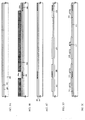
- CMOS circuit is shown as a basic circuit for the driver circuits.
- a base film 301 is formed with a 300 nm thickness on a glass substrate 300.
- Silicon nitride oxide films are laminated as the base film 302 in embodiment 1. It is good to set the nitrogen concentration at between 10 and 25 wt% in the film contacting the glass substrate 300.
- an amorphous silicon film (not shown in the figures) is formed with a thickness of 50 nm on the base film 301 by a known deposition method. Note that it is not necessary to limit this to the amorphous silicon film, and another film may he formed provided that it is a semiconductor film containing an amorphous structure (including a microcrystalline semiconductor film). In addition, a compound semiconductor film containing an amorphous structure, such as an amorphous silicon germanium film, may also be used. Further, the film thickness may be made from 20 to 100 nm.
- the amorphous silicon film is then crystallized by a known technique, forming a crystalline silicon film (also referred to as a polycrystalline silicon film or a polysilicon film) 302.
- a crystalline silicon film also referred to as a polycrystalline silicon film or a polysilicon film
- Thermal crystallization using an electric furnace, laser annealing crystallization using a laser, and lamp annealing crystallization using an infrared light exist as known crystallization methods. Crystallization is performed in embodiment 1 using light from an excimer laser which uses XeCl gas.
- pulse emission type excimer laser light formed into a linear shape is used in embodiment 1, but a rectangular shape may also be used, and continuous emission argon laser light and continuous emission excimer laser light can also be used.
- the crystalline silicon film is used as the active layer of the TFT, it is also possible to use an amorphous silicon film. Note that it is possible to form the active layer of the switching TFT, in which there is a necessity to reduce the off current, by the amorphous silicon film, and to form the active layer of the current control TFT by the crystalline silicon film. Electric current flows with difficulty in the amorphous silicon film because the carrier mobility is low, and the off current does not easily flow. In other words, the most can be made of the advantages of both the amorphous silicon film, through which current does not flow easily, and the crystalline silicon film, through which current easily flows.
- a protecting film 303 is formed on the crystalline silicon film 302 with a silicon oxide film having a thickness of 130 nm. This thickness may be chosen within the range of 100 to 200 nm (preferably between 130 and 170 nm). Furthermore, other films may also be used providing that they are insulating films containing silicon.
- the protecting film 303 is provided so that the crystalline silicon film is not directly exposed to plasma during addition of an impurity, and so that delicate concentration control of the impurity is possible.
- Resist masks 304a and 304b are then formed on the protecting film 303, and an impurity element which imparts n-type conductivity (hereafter referred to as an n-type impurity element) is added.
- an impurity element which imparts n-type conductivity hereafter referred to as an n-type impurity element
- elements residing in periodic table group 15 are generally used as the n-type impurity element, and typically phosphorous or arsenic can be used.
- a plasma doping method is used, in which phosphine (PH 3 ) is plasma activated without separation of mass, and phosphorous is added at a concentration of 1x10 18 atoms/cm 3 in embodiment 1.
- phosphine phosphine
- phosphorous is added at a concentration of 1x10 18 atoms/cm 3 in embodiment 1.
- an ion implantation method in which separation of mass is performed, may also be used.
- the dose amount is regulated so that the n-type impurity element is contained in n-type impurity regions 305 and 306, thus formed by this process, at a concentration of 2x10 16 to 5x10 19 atoms/cm 3 (typically between 5x10 17 and 5x10 18 atoms/cm 3 ).
- the protecting film 303 is removed, and an activation of the added periodic table group 15 elements is performed.
- a known technique of activation may be used as the means of activation, and activation is done in embodiment 1 by irradiation of excimer laser light.
- a pulse emission type excimer laser and a continuous emission type excimer laser may both, of course, be used, and it is not necessary to place any limits on the use of excimer laser light.
- the object is the activation of the added impurity element, and it is preferable that irradiation is performed at an energy level at which the crystalline silicon film does not melt. Note that the laser irradiation may also be performed with the protecting film 303 in place.
- the activation by heat treatment may also be performed along with activation of the impurity element by laser light.
- activation is performed by heat treatment, considering the heat resistance of the substrate, it is good to perform heat treatment on the order of 450 to 550°C.
- a boundary portion (connecting portion) with regions along the edges of the n-type impurity regions 305 and 306, namely regions along the periphery into which the n-type impurity element, which exists in the n-type impurity regions 305 and 306, is not added, is delineated by this process. This means that, at the point when the TFTs are later completed, extremely good connections can be formed between LDD regions and channel forming regions.
- a gate insulating film 311 is formed, covering the active layers 307 to 310.
- a single layer structure or a lamination structure may be used.
- a 110 nm thick silicon nitride oxide film is used in embodiment 1.
- a conductive film having a thickness of 200 to 400 nm is formed, and patterning is carried out to form gate electrodes 312 to 316.
- the end portions of the gate electrodes 312 to 316 can also be made taper-shaped.
- the gate electrode and an extended wiring line (hereinafter referred to as a gate wiring line) electrically connected to the gate electrode are formed of different materials. Specifically, a material having a resistance lower than the gate electrode is used for the gate wiring line. This is because a material which can be finely worked is used for the gate electrode and a material which has a low wiring resistance though fine working can not be made is used for the gate wiring line.
- the gate electrode and the gate wiring line may be formed of the same material.
- the gate electrode may be formed of a conductive film of a single layer, it is preferable to make a laminate film such as a two-layer or three-layer film as the need arises.
- a laminate film such as a two-layer or three-layer film
- any well-known conductive films may be used. However, as described above, it is preferable to use a material which can be finely worked, specifically, can be patterned into a line width of 2 ⁇ m or less.
- the films may be used as a single layer or a laminate layer.
- a laminate film of a tungsten nitride (WN) film having a thickness of 50 nm and a tungsten (W) film having a thickness of 350 nm is used. These may be formed by a sputtering method. When an inert gas of Xe, Ne or the like is added as a sputtering gas, film peeling due to stress can be prevented.
- the gate electrodes 313 and 316 are formed at this time so as to overlap a portion of the n-type impurity regions 305 and 306, respectively, sandwiching the gate insulating film 311. This overlapping portion later becomes an LDD region overlapping the gate electrode.
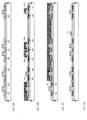
- an n-type impurity element (phosphorous is used in embodiment 1) is added in a self-aligning manner with the gate electrodes 312 to 316 as masks, as shown in Fig. 4A.
- the addition is regulated so that phosphorous is added to impurity regions 317 to 323 thus formed at a concentration of 1/2 to 1/10 that of the impurity regions 305 and 306 (typically between 1/3 and 1/4).
- a concentration of 1x10 16 to 5x10 18 atoms/cm 3 (typically 3x10 17 to 3x10 18 atoms/cm 3 ) is preferable.
- Resist masks 324a to 324c are formed next, with a shape covering the gate electrodes etc., as shown in Fig. 4B, and an n-type impurity element (phosphorous is used in embodiment 1) is added, forming impurity regions 325 to 331 containing a high concentration of phosphorous.
- Ion doping using phosphine (PH 3 ) is also performed here, and is regulated so that the phosphorous concentration of these regions is from 1x10 20 to 1x10 21 atoms/cm 3 (typically between 2x10 20 and 5x10 21 atoms/cm 3 ).
- a source region or a drain region of the n-channel TFT is formed by this process, and in the switching TFT, a portion of the n-type impurity regions 320 to 322 formed by the process of Fig. 4A remains.
- the resist masks 324a to 324c are removed, and a new resist mask 332 is formed.
- a p-type impurity element (boron is used in embodiment 1) is then added, forming impurity regions 333 and 334 containing a high concentration of boron.
- Boron is added here at a concentration of 3x10 20 to 3x10 21 atoms/cm 3 (typically between 5x10 20 and 1x10 21 atoms/cm 3 ) by ion doping using diborane (B 2 H 6 ).
- phosphorous has already been added to the impurity regions 333 and 334 at a concentration of 1x10 20 to 1x10 21 atoms/cm 3 , but boron is added here at a concentration of at least 3 times more than that of the phosphorous. Therefore, the n-type impurity regions already formed completely invert to p-type, and function as p-type impurity regions.
- the n-type or p-type impurity element added at each concentration is activated.
- activating means a furnace annealing method, a laser annealing method, or a lamp annealing method can be used.
- a heat treatment in a nitrogen atmosphere at 550°C for 4 hours is carried out in an electric heating furnace.
- an oxygen concentration in the treatment atmosphere at the activation step is made 1 ppm or less, preferably 0.1 ppm or less.
- a gate wiring line 335 having a thickness of 300 nm is formed.
- a metal film containing aluminum (Al) or copper (Cu) as its main ingredient (constituting 50 to 100%) may be used.
- it is formed so as to electrically connect the gate electrodes 314 and 315 of the switching TFT (Fig. 4D).
- the wiring resistance of the gate wiring line can be made very low, so that an image display region (pixel portion) with a large area can be formed. That is, the pixel structure of this embodiment is very effective in realization of an EL display device having a screen of a size of not less than 10 inches in diagonal (further, 30 cm or more).
- a first interlayer insulating film 336 is formed.
- the first interlayer insulating film 336 a single layer of an insulating film containing silicon may be used, or a laminate film of a combination of such films may be used. Besides, it is appropriate that the film thickness is made 400 nm to 1.5 ⁇ m. In this embodiment, such a structure is formed that a silicon oxide film with a thickness of 800 nm is laminated on a silicon nitride oxide film with a thickness of 200 nm.
- heat treatment is performed for 1 to 12 hours at 300 to 450°C in an atmosphere containing between 3 and 100% hydrogen, performing hydrogenation.
- This process is one of hydrogen termination of dangling bonds in the semiconductor film by hydrogen which is thermally activated.
- Plasma hydrogenation (using hydrogen activated by a plasma) may also be performed as another means of hydrogenation.
- the hydrogenation step may also be inserted during the formation of the first interlayer insulating film 336. Namely, hydrogen processing may be performed as above after forming the 200 nm thick silicon nitride oxide film, and then the remaining 800 nm thick silicon oxide film may be formed.
- this electrode is made of a laminate film of three-layer structure in which a titanium film having a thickness of 100 nm, an aluminum film containing titanium and having a thickness of 300 nm, and a titanium film having a thickness of 150 nm are continuously formed by a sputtering method.
- a titanium film having a thickness of 100 nm, an aluminum film containing titanium and having a thickness of 300 nm, and a titanium film having a thickness of 150 nm are continuously formed by a sputtering method.
- other conductive films may be used.
- a first passivation film 344 is formed next with a thickness of 50 to 500 nm (typically between 200 and 300 nm).
- a 300 nm thick silicon nitride oxide film is used as the first passivation film 344 in embodiment 1. This may also be substituted by a silicon nitride film.
- a second interlayer insulating film 345 made of organic resin is formed.
- the organic resin it is possible to use polyimide, polyamide, acryl, BCB (benzocyclobutene) or the like.
- the second interlayer insulating film 345 is primarily used for flattening, acryl excellent in flattening properties is preferable.
- an acrylic film is formed to a thickness sufficient to flatten a stepped portion formed by TFTs. It is appropriate that the thickness is preferably made 1 to 5 ⁇ m (more preferably, 2 to 4 ⁇ m).
- a contact hole reaching the drain wiring line 343 is formed in the second interlayer insulating film 345 and the first passivation film 344, and a pixel electrode 346 is formed.
- a pixel electrode 346 an aluminum alloy film (aluminum film containing titanium of 1 wt%) with a thickness of 300 nm is formed.
- reference numeral 347 designates an end portion of an adjacent pixel electrode.
- an alkaline compound 348 is formed.
- a lithium fluoride film is formed by an evaporation method to a thickness of 5 nm.
- an EL layer 349 with a thickness of 100 nm is formed thereon by a spin coating method.
- polymer organic materials such as polyparaphenylene vinylene (PPV) or polyfluorene and low molecular organic materials can be cited.
- PV polyparaphenylene vinylene
- polyfluorene and low molecular organic materials can be cited.
- the polymer organic material showing white luminescence, which becomes an luminescent layer materials disclosed in Japanese Patent Application Laid-Open No. Hei. 8-96959 or No. Hei. 9-63770 may be used.
- a material obtained by dissolving PVK polyvinylcarbazole
- Bu-PBD (2-(4'-tert-butylphenyl)-5-(4'-biphenyl)-1,3,4-oxadiazole)
- coumarin 6 DCM1 (4-dicyanomethylene-2-methyl-6-p-dimethylaminostyryl-4H-pyrane), TPB (tetraphenylbutadiene), or Nile red in 1,2-dichloromethane
- the film thickness is made 30 to 150 nm (preferably, 40 to 100 nm).
- the above example is merely an example of organic materials which can be used for the EL layer of the present invention, and does not limit the present invention.
- the EL layer 349 a well-known material and structure may be used. However, in the present invention, a low molecular organic material capable of emitting white light was used. Note that the color filters corresponding to RGB may be positioned above the pixel electrode on the active matrix substrate. Besides, such a structure may be adopted that another substrate is bonded to the active matrix substrate so as to seal the EL element, and the color filters are provided on that substrate. Note that the color filters are not shown for simplification.
- a color display system in which an EL layer of blue or blue-green luminescence and a fluorescent material (fluorescent color conversion layer: CCM) are combined, or a system in which color display is made by stacking EL layers corresponding to RGB.
- CCM fluorescent color conversion layer
- the EL layer 349 is made a single layer structure of only the above luminescent layer, as the need arises, an electron injection layer, an electron transport layer, a hole transport layer, a hole injection layer, an electron blocking layer or a hole blocking layer may be provided.
- an anode 350 having a thickness of 200 nm and made of a transparent conductive film is formed to cover the EL layer 349.
- a film made of a compound of indium oxide and zinc oxide is formed by an evaporation method, and patterning is carried out to make an anode.
- a second passivation film 351 made of a silicon nitride film is formed to a thickness of 100 nm.
- This second passivation film 351 protects the EL layer 349 against moisture or the like. Besides, it also serves to release heat generated in the EL layer 349. In order to further raise the heat dissipation effect, it is also effective to laminate a silicon nitride film and a carbon film (preferably a diamond-like carbon film) to make a second passivation film.
- an active matrix EL display device having a structure as shown in Fig. 5C is completed.
- a TFT having an optimum structure is disposed in not only the pixel portion but also the driving circuit portion, so that very high reliability is obtained and operation characteristics can also be improved.
- a TFT having a structure to decrease hot carrier injection so as not to drop the operation speed thereof as much as possible is used as an n-channel TFT of a CMOS circuit forming a driving circuit.
- the driving circuit here includes a shift register, a buffer, a level shifter, a sampling circuit (sample and hold circuit) and the like.
- a signal conversion circuit such as a D/A converter can also be included.
- the active layer of the n-channel TFT 205 includes a source region 355, a drain region 356, an LDD region 357 and a channel formation region 358, and the LDD region 357 overlaps with the gate electrode 313, putting the gate insulating film 311 therebetween.
- the LDD region 357 is made to completely overlap with the gate electrode to decrease a resistance component to a minimum. That is, it is preferable to remove the so-called offset.
- an LDD region does not need to be particularly provided.
- the sampling circuit is somewhat unique compared with the other sampling circuits, in that a large electric current flows in both directions in the channel forming region. Namely, the roles of the source region and the drain region are interchanged. In addition, it is necessary to control the value of the off current to be as small as possible, and with that in mind, it is preferable to use a TFT having functions which are on an intermediate level between the switching TFT and the current control TFT in the sampling circuit.
- the foregoing structure can be easily realized by manufacturing TFTs in accordance with the manufacturing steps shown in Figs. 3A to 5C.
- a logical circuit such as a signal dividing circuit, a D/A converter circuit, an operational amplifier circuit, or the like other than the driving circuit on the same substrate, and further, it is believed that a memory portion, a microprocessor, or the like can be formed.
- a sealing material also referred to as a housing material
- a sealing material 18 is formed at this time so as to surround at least the pixel portion, and preferably the driver circuits and the pixel portion (Fig.6).
- a plate shape material possessing a concave portion so as to surround the element portion may also be used as the sealing material 18, and that ultraviolet hardened resin may also be used.
- the EL element is in a state of being completely enclosed in the airtight space at this point, and is completely cutoff from the atmosphere.
- a gap 20 between the sealing material 18 and the substrate 10 is desirable to fill a gap 20 between the sealing material 18 and the substrate 10 with an inert gas (argon, helium, nitrogen, etc.) or to provide a drying agent such as barium oxide in the gap.
- an inert gas argon, helium, nitrogen, etc.
- a drying agent such as barium oxide
- a connector flexible printed circuit: FPC 17
- FPC 17 flexible printed circuit
- reference numeral 300 designates a substrate; 11, a pixel portion; 12, a source side driving circuit; and 13, a gate side driving circuit.
- the respective driving circuits reach an FPC 17 through wiring lines 14 to 16 and are connected to an external equipment.
- an image can be displayed on the pixel portion by connecting the FPC 17 to a terminal of the external equipment.
- an article which comes to have a state where image display can be made by attaching an FPC is defined as an EL display device.
- an EL element is formed of a pixel electrode (anode) made of ITO / EL layer / MgAg electrode (cathode) in sequence from below.
- output light of the EL element is outputted to the substrate side (lower surface side of the active matrix substrate) at which a TFT is formed.
- the example in which the low molecular organic material giving white luminescence is used as the EL material constituting the EL layer has been described.
- this embodiment an example in which three kinds of polymer organic material layers corresponding to R (red), G (green) and B (blue) are stacked, will be described. Note that since this embodiment is different from the embodiment 1 only in the EL materials, only that point will be described.
- polymer organic materials polyparaphenylene vinylene (PPV), polyfluorene, etc.
- PV polyparaphenylene vinylene
- cyanopolyphenylenevinylene was used for a red luminescent material
- polyphenylenevinylene was used for a green luminescent material
- polyphenylenevinylene and polyalkylphenylene were used for a blue luminescent material.
- luminescence red luminescence, green luminescence, and blue luminescence
- luminescence red luminescence, green luminescence, and blue luminescence
- Laser crystallization is used as the means of forming the crystalline silicon film 302 in embodiment 1, and a case of using a different means of crystallization is explained in embodiment 3.
- crystallization is performed using the technique recorded in Japanese Patent Application Laid-open No. Hei 7-130652.
- the technique described in the above patent application is one of obtaining a crystalline silicon film having good crystallinity by using an element such as nickel as a catalyst for promoting crystallization.
- the catalyst may be gettered using the technique recorded in Japanese Patent Application Laid-open No. Hei 10-270363 or Japanese Patent Application Laid-open No. Hei 8-330602.
- a TFT may be formed using the technique recorded in the specification of Japanese Patent Application No. Hei 11-076967 by the applicant of the present invention.
- top gate type TFTs were explained by embodiment 1, but the present invention is not limited to a TFT structure, and it may also be implemented using a bottom gate type TFT (typically an inverted stagger type TFT). Further, the inverted stagger type TFT may be formed by any means.
- the inverted stager type TFT is a good structure having fewer processes than the top gate type TFT, and it is therefore extremely advantageous in lowering manufacturing costs, an object of the present invention. Note that it is possible to freely combine the constitution of embodiment 4 with the constitution of embodiment 2 and embodiment 3.
- the EL display device fabricated in accordance with the present invention is of the self-emission type, and thus exhibits more excellent recognizability of the displayed image in a light place as compared to the liquid crystal display device. Furthermore, the EL display device has a wider viewing angle. Accordingly, the EL display device can be applied to a display portion in various electronic devices. For example, in order to view a TV program or the like on a large-sized screen, the EL display device in accordance with the present invention can be used as a display portion of an EL display (i.e., a display in which an EL display device is installed into a frame) having a diagonal size of 30 inches or larger (typically 40 inches or larger.)
- the EL display includes all kinds of displays to be used for displaying information, such as a display for a personal computer, a display for receiving a TV broadcasting program, a display for advertisement display. Moreover, the EL display device in accordance with the present invention can be used as a display portion of other various electric devices.
- Such electronic devices include a video camera, a digital camera, a goggles-type display (head mount display), a car navigation system, a car audio equipment, note-size personal computer, a game machine, a portable information terminal (a mobile computer, a portable telephone, a portable game machine, an electronic book, or the like), an image reproduction apparatus including a recording medium (more specifically, an apparatus which can reproduce a recording medium such as a compact disc (CD), a laser disc (LD), a digital video disc (DVD), and includes a display for displaying the reproduced image), or the like.
- a recording medium more specifically, an apparatus which can reproduce a recording medium such as a compact disc (CD), a laser disc (LD), a digital video disc (DVD), and includes a display for displaying the reproduced image
- Figs. 8A to 8F respectively show various specific examples of such electronic devices.
- Fig, 8A illustrates an EL display which includes a frame 2001, a support table 2002, a display portion 2003, or the like.
- the present invention is applicable to the display portion 2003.
- the EL display is of the self-emission type and therefore requires no back light.
- the display portion thereof can have a thickness thinner than that of the liquid crystal display device.
- Fig. 8B illustrates a video camera which includes a main body 2101, a display portion 2102, an audio input portion 2103, operation switches 2104, a battery 2105, an image receiving portion 2106, or the like.
- the EL display device in accordance with the present invention can be used as the display portion 2102.
- Fig. 8C illustrates a portion (the right-half piece) of an EL display of head mount type, which includes a main body 2201, signal cables 2202, a head mount band 2203, a display portion 2204, an optical system 2205, an EL display device 2206, or the like.
- the present invention is applicable to the EL display device 2206.
- Fig. 8D illustrates an image reproduction apparatus including a recording medium (more specifically, a DVD reproduction apparatus), which includes a main body 2301, a recording medium (a CD, an LD, a DVD or the like) 2302, operation switches 2303, a display portion (a) 2304, another display portion (b) 2305, or the like.
- the display portion (a) is used mainly for displaying image information
- the display portion (b) is used mainly for displaying character information.
- the EL display device in accordance with the present invention can be used as these display portions (a) and (b).
- the image reproduction apparatus including a recording medium further includes a CD reproduction apparatus, a game machine or the like.
- Fig. 8E illustrates a portable (mobile) computer which includes a main body 2401, a camera portion 2402, an image receiving portion 2403, operation switches 2404, a display portion 2405, or the like.
- the EL display device in accordance with the present invention can be used as the display portion 2405.
- Fig. 8F illustrates a personal computer which includes a main body 2501, a frame 2502, a display portion 2503, a keyboard 2504, or the like.
- the EL display device in accordance with the present invention can be used as the display portion 2503.
- the EL display device in accordance with the present invention will be applicable to a front-type or rear-type projector in which light including output image information is enlarged by means of lenses or the like to be projected.
- a portion of the EL display device that is emitting light consumes power, so it is desirable to display information in such a manner that the light emitting portion therein becomes as small as possible. Accordingly, when the EL display device is applied to a display portion which mainly displays character information, e.g., a display portion of a portable information terminal, and more particular, a portable telephone or a car audio equipment, it is desirable to drive the EL display device so that the character information is formed by a light-emitting portion while a non-emission portion corresponds to the background.
- character information e.g., a display portion of a portable information terminal, and more particular, a portable telephone or a car audio equipment
- a portable telephone which includes a main body 2601, an audio output portion 2602, an audio input portion 2603, a display portion 2604, operation switches 2605, and an antenna 2606.
- the EL display device in accordance with the present invention can be used as the display portion 2604.
- the display portion 2604 can reduce power consumption of the portable telephone by displaying white-colored characters on a black-colored background.
- Fig. 9B illustrates a car audio equipment which includes a main body 2701, a display portion 2702, and operation switches 2703 and 2704.
- the EL display device in accordance with the present invention can be used as the display portion 2702.
- the car audio equipment of the mount type is shown in the present embodiment, the present invention is also applicable to a car audio of the set type.
- the display portion 2702 can reduce power consumption by displaying white-colored characters on a black-colored background, which is particularly advantageous for the car audio of the set type.
- the present invention can be applied variously to a wide range of electronic devices in all fields.
- the electronic device in the present embodiment can be obtained by utilizing an EL display device having the configuration in which the structures in Embodiments 1 through 4 are freely combined.
- the EL display device including the EL element emitting light with the suitably controlled luminescent brightness is fabricated.
- the EL display device of the present invention as a display portion, an inexpensive electronic device with high visibility can be obtained.
Abstract
Description
- The present invention is related to an EL (electroluminescence) display device formed by a semiconductor element (an element using a semiconductor thin film, typically a thin-film transistor) built on a substrate, and to an electronic device having the EL display device as a display portion.
- Techniques of forming a thin-film transistor (hereafter referred to as a TFT) on a substrate have greatly advanced in recent years, and development of applications to active matrix display devices is proceeding. In particular, a TFT using a polysilicon film has a higher electric field effect mobility than a TFT using a conventional amorphous silicon film, and therefore it is capable of high speed operation. It therefore becomes possible to perform control of a pixel, conventionally performed by a driver circuit external to the substrate, by a driver circuit formed on the same substrate as the pixel.
- This type of active matrix display device is gaining attention for obtaining many advantages, such as lowered manufacturing cost, smaller display device, increased yield, and reduced throughput, by building various circuits and elements on the same substrate.
- In addition, research on active matrix EL display devices having EL elements as self-luminescing elements has become spirited. The EL display device is also referred to as organic EL display (OELD) or an organic light emitting diode (OLED).
- The EL display device is a self luminescing type which differs from a liquid crystal display device. The EL element has a structure in which an EL layer is sandwiched between a pair of electrodes, and the EL layer is normally a lamination structure. A lamination structure of a hole transporting layer, a light emitting layer, and an electron transporting layer proposed by Tang, et al., of Eastman Kodak Co. can be given as a typical structure. This structure has extremely high light emitting efficiency, and nearly all EL display devices in which research and development is proceeding employ this structure.
- Furthermore, additional structures such as a hole injecting layer, a hole transporting layer, a light emitting layer, and an electron transporting layer formed in order on a pixel electrode; or a hole injecting layer, a hole transporting layer, a light emitting layer, an electron transporting layer, and an electron injecting layer formed in order on a pixel electrode may also be used. An element such as a fluorescing pigment may also be doped into the EL layer.
- A predetermined voltage is then applied to the EL layer having the above structure by a pair of electrodes, and recombination of a carrier thus occurs in the light emitting layer, and light is emitted.
- The EL display device has roughly four colorizing display systems, that is, a system in which an EL element of white luminescence and color filters are combined, a system in which three kinds of EL elements corresponding to R (red), G (green) and B (blue) are formed, a system in which an EL element of blue or blue-green luminescence and a fluorescent material (fluorescent color converting layer: CCM) are combined, and a system in which a transparent electrode is used as a cathode (counter electrode) and EL elements corresponding to RGB are overlapped.
- The color filter is a color filter for extracting light of red, green or blue. The color filter is formed at a position corresponding to a pixel, and the color of extracted light at each pixel can be changed by this. This is the same as a colorizing system of a liquid crystal display device using color filters in principal. Note that the position corresponding to the pixel indicates a position coincident with a pixel electrode.
- However, the color filter is a filter which extracts the light of a specified wavelength to improve the color purity of the transmitted tight. Thus, in the case where a tight component of a wavelength to be extracted is small, there can occur such a disadvantage that the brightness of the light of the wavelength is extremely low or the color purity is poor.
- In well-known organic EL materials, a red with high luminescent brightness has not been realized, and like an example shown in Fig. 10, the luminescent brightness of red is low as compared with the luminescent brightness of blue or green. In the case where an organic EL material having such luminescent characteristics is used for an EL display device, the luminescent brightness of red of an image to be displayed becomes poor.
- Further, a method of using orange color light having a slightly lower wavelength than that of red color light has been conventionally performed because the brightness of red color light is low compared to the brightness of blue and green light. However, in this case the brightness of red color images which are displayed by the EL display device is low, and when display of the red color image is attempted, it is displayed as orange.
- In consideration of the above, an object of the present invention is to provide an EL display device for displaying an image which has a desirable good balance between the brightnesses of red, blue, and green light in EL elements with different brightness of red, blue and green.
- According to an aspect of the present invention, an electronic device includes an EL display device having a TFT, a pixel electrode electrically connected to the TFT, an EL element with the pixel electrode as a cathode or an anode, and an insulating layer for sealing the EL element; means for applying an analog image signal to the EL element; and means for gamma (γ)-correcting the analog image signal.
- The above structure may further include a memory for storing data for gamma (γ) correction.
- According to another aspect of the present invention, an EL display device includes, on a same substrate, a TFT, a pixel electrode electrically connected to the TFT, an EL element with the pixel electrode as a cathode or an anode, an insulating layer for sealing the EL element, means for applying an analog image signal to the EL element, and means for gamma (γ)-correcting the analog image signal.
- The above structure may further include a memory for storing data for gamma (γ) correction on the same substrate.
- Besides, in the EL display device, a color filter is formed at a position corresponding to the pixel electrode for colorization.
- Besides, for colorization by using another method, the EL element may be formed of a first pixel including a blue luminescent layer, a second pixel including a green luminescent layer, and a third pixel including a red luminescent layer. In this case, the color filter may be used or may not be used.
- Besides, in the above EL display device, the gamma (γ) correction may amplify a signal of red, or may attenuate a signal of blue or green. Besides, the gamma (γ) correction may be independently made for each of signals of blue, green and red.
- By adopting the foregoing structure, even in the case of using an EL material in which a red light component of a wavelength to be extracted by the color filter is small, it is possible to provide an EL display device displaying an image of a desired RGB (red, blue, green) balance by making the gamma (γ) correction to, for example, a video signal to adjust the luminescent brightness of RGB (red, blue, green).
-
- Fig. 1 is a circuit block diagram of an EL display device of the present invention.
- Fig. 2 is a structural view when a gamma (γ) correction table of the EL display device of the present invention is prepared.
- Figs. 3A to 3E are views showing a fabricating process of an active matrix EL display device of Embodiment 1.
- Figs. 4A to 4D are views showing the fabricating process of the active matrix EL display device of Embodiment 1.
- Figs. 5A to 5C are views showing the fabricating process of the active matrix EL display device of Embodiment 1.
- Fig. 6 is a sectional view of an EL display device of Embodiment 1.
- Fig. 7 is a top view of an EL display device of Embodiment 1.
- Figs. 8A to 8F are views showing examples of electronic instruments of Embodiment 5.
- Fig. 9A and 9B are views showing examples of electronic instruments of Embodiment 5.
- Fig. 10 is a view showing characteristics between the luminescent brightness of EL elements (R, G, B) and current density.
-
- First, an embodiment mode of carrying out the present invention will be described with reference to Figs. 1 and 2.
- Fig. 1 is a block diagram showing an EL display device of the present invention. In Fig. 1,
reference numeral 100 designates an active matrix substrate which includessource driver circuits gate driver circuit 130, and apixel portion 150. Thepixel portion 150 includes pixels arranged in matrix form, and each pixel includes aTFT 151, anEL element 152, and the like. Although not shown for simplification, in this embodiment, colorization is realized by using color filters corresponding to R (red), G (green) and B (blue). -
Reference numeral 160 designates an image signal processing circuit which includes an A/D conversion circuit 163 for converting an analog signal inputted from the outside into a digital signal, acorrection circuit 161 for correcting the digital signal, and a D/A conversion circuit 164 for converting the corrected digital signal into an analog signal. Thecorrection circuit 161 includes acorrection memory 162. In the display device of the present invention, avideo signal 200 is gamma (γ)-corrected. For example, thevideo signal 200 is corrected on the basis of a gamma (γ) correction table stored in the correction memory. - A
control circuit 170 controls various signals supplied to theactive matrix substrate 100 and the imagesignal processing circuit 160. Asynchronous signal 210 is inputted to thecontrol circuit 170. - The
control circuit 170 is a circuit for forming and supplying pulses (start pulse, clock pulse, synchronous signal, etc.) necessary for controlling thesource driver circuits gate driver circuit 130, the imagesignal processing circuit 160, and the like on the basis of thesynchronous signal 210. - Note that the
control circuit 170 repeats an operation (frequency dividing) for counting a previously set count number (frequency division ratio) of clocks, while the inputtedsynchronous signal 210 is made a reference and an oscillation clock signal (OSC) outputted from a phase synchronized oscillator is made an original oscillation. The clocks are counted at the same time as this frequency dividing to form a start pulse (S_SP) supplied to the source driver circuit in the horizontal direction of a screen and a clock pulse (S_CK), a start pulse (G_SP) supplied to the gate driver circuit in the vertical direction of a screen and a clock pulse (G_CK), a clock pulse (D_CK), and the like. Further, there is also a case where a horizontal synchronous signal (HSY) and a vertical synchronous signal (VSY) are formed. - The image
signal processing circuit 160, thecontrol circuit 170, and the like are mounted on a substrate different from theactive matrix substrate 100, for example, another printed substrate, and circuits on the substrate and theactive matrix substrate 100 are connected through a cable, a flexible wiring plate, and the like. Note that it is needless to say that it is preferable to make such a structure that a part or all of circuits such as the imagesignal processing circuit 160, thecontrol circuit 170, and the like are provided on the same substrate as the active matrix substrate since integration and miniaturization are realized. - The
video signal 200 inputted to the imagesignal processing circuit 160 from the outside is an analog signal. Thevideo signal 200 may be an analog signal such as a television signal or a video signal, or may be an analog signal formed by D/A conversion of a data signal from a computer or the like. - In the image
signal processing circuit 160, thevideo signal 200 is converted into a digital video signal by the A/D conversion circuit 163 and is outputted to thecorrection circuit 161. Thecorrection circuit 161 makes gamma (γ) correction, in view of the luminescent brightness of each EL element, to the inputted digital video signal on the basis of the gamma (γ) correction table stored in the correction memory. - In the gamma (γ) correction, a supplied image signal is corrected in order to obtain excellent gradation display. The gamma (γ)-corrected digital video signal is converted into an analog video signal by the D/
A conversion circuit 164 and is supplied to thesource driver circuits - By this
correction circuit 161, a video signal supplied to each EL element is gamma (γ)-corrected, and the luminescent brightness of each of blue luminescence, green luminescence and red luminescence can be suitably controlled in accordance with the voltage and current of the corrected analog video signal. For example, in the case where an EL element using three kinds (R, G, B) of color filters as shown n Fig. 10 is used, the video signal (corresponding to R) has only to be gamma (γ)-corrected to increase the luminescent brightness of R so that the luminescent brightness of each color becomes identical. Alternatively, the video signal applied to the EL element (corresponding to B or G) has only to be gamma (γ)-corrected to decrease the luminescent brightness of B or G so that the luminescent brightness of each color becomes identical. In addition, the video signals applied to the respective EL elements may be gamma (γ)-corrected to increase the luminescent brightness of R and to decrease the luminescent brightness of B or G so that the luminescent brightness of each color becomes identical. - Here, an example of a preparation method of the gamma (γ) correction table of the correction memory in the correction circuit of the image
signal processing circuit 160 of the present invention will be described. - Reference will be made to Fig. 2. Fig. 2 is a circuit block diagram in the case where the gamma (γ) correction table of the correction memory in the correction circuit of the image
signal processing circuit 160 of the present invention is prepared.Reference numeral 201 designates an image pickup device which converts an image displayed by the luminescence of the EL element into an electric signal. - As the
image pickup device 201, another image pickup device such as a CCD camera or a digital video camera can be used. Alternatively, a luminance meter or an illuminance meter for merely measuring the lightness or brightness of a displayed image may be used. In the case where the luminance meter or the illuminance meter is used, it is appropriate that an A/D conversion circuit for converting a signal supplied from these devices into a digital signal is used. -
Reference numeral 202 designates a digital signal processor (DSP); 203, a reference signal supply source; and 204, a signal generator (SG). - The
correction circuit 161 of the imagesignal processing circuit 160 gamma (γ)-corrects a digital signal supplied from thesignal generator 204, outputs a digital video signal after correction, converts the signal into an analog video signal by the D/A conversion circuit, and sends it to the respective EL elements. The respective EL elements emit light on the basis of the analog video signal supplied from the imagesignal processing circuit 160 and display an image. - The displayed image is made a digital signal by using the
image pickup device 201. The digital signal sent from theimage pickup device 200 is supplied to the digital signal processor (DSP) 202. Thedigital signal processor 202 compares the digital signal supplied from theimage pickup device 201 with a digital signal supplied from the referencedata supply source 203, and feeds back the discrepancy of the data to thecorrection circuit 161. Note that the reference data may be directly supplied from thesignal generator 204. - In accordance with the signal supplied from the
digital signal processor 202, thecorrection circuit 161 further corrects the digital signal from thesignal generator 204, converts it into an analog video signal, and again sends it to the EL element. The respective EL elements emit light on the basis of the analog video signal supplied from the imagesignal processing circuit 160 and display an image. - The displayed image is again made a digital signal by using the
image pickup device 201. The digital signal supplied from theimage pickup device 201 is sent to thedigital signal processor 202. Thedigital signal processor 202 compares the digital signal supplied from theimage pickup device 201 with the digital signal supplied from the referencedata supply source 203, and feeds back the discrepancy to thecorrection circuit 161. - When suitable data of gamma (γ) correction are obtained in this way, the data are stored at an appointed address of the
correction memory 162. - Thereafter, in order to start the correction of a next video signal, the
signal generator 204 sends a digital signal different from the previous one to thecorrection circuit 161. When suitable data of gamma (γ) correction to the digital signal are obtained, the data are stored at an appointed address of thecorrection memory 162. - When all correction data are stored in the
correction memory 162, thesignal generator 204 and thedigital signal processor 202 are separated from theactive matrix substrate 100. Here, the preparation of the gamma (γ) correction table is completed. Note that the method of preparing the gamma (γ) correction table shown here is merely an example, and it is needless to say that the present invention is not particularly limited. Besides, the block circuit diagram of Fig. 1 is also an example, and it is also possible to make gamma (γ) correction by using, for example, a correction circuit without a correction memory. - Thereafter, a digital video signal is supplied to the
correction circuit 160, and on the basis of the data of the gamma (γ) correction table stored in thecorrection memory 161, the digital video signal is corrected, and after the signal is further converted into an analog video signal, it is supplied to the EL element. Since the suitable correction is made to the analog video signal supplied to the EL element by thecorrection circuit 160, balanced luminescence (red luminescence, green luminescence, and blue luminescence) is obtained and an excellent image is displayed. - The present invention having the above structure will be described in more detail with reference to the following embodiments.
- In this embodiment, an EL display device provided with a correction circuit will be described with reference to Fig. 1.
- Fig. 1 is a block diagram showing an EL display device of this embodiment. In Fig. 1,
reference numeral 100 designates an active matrix substrate which includessource driver circuits gate driver circuit 130, and apixel portion 150. Thepixel portion 150 includes pixels arranged in matrix form, and each pixel includes aTFT 151, anEL element 152, and the like. Although not shown for simplification, in this embodiment, colorization is realized by using color filters corresponding to R (red), G (green) and B (blue). -
Reference numeral 160 designates an image signal processing circuit which includes an A/D conversion circuit 163 for converting an analog signal inputted from the outside into a digital signal, acorrection circuit 161 for gamma (γ)-correcting the digital signal, and a D/A conversion circuit 164 for converting the gamma (γ)-corrected digital signal into an analog signal. Thecorrection circuit 161 includes acorrection memory 162. -
Reference numeral 170 designates a control circuit which controls various signals supplied to theactive matrix substrate 100 and the imagesignal processing circuit 160. Asynchronous signal 210 is inputted to thecontrol circuit 170. - The image
signal processing circuit 160, thecontrol circuit 170, and the like are mounted on a substrate different from theactive matrix substrate 100, for example, another printed substrate, and circuits on the substrate and theactive matrix substrate 100 are connected through a cable, a flexible wiring plate, and the like. - A
video signal 200 inputted to the imagesignal processing circuit 160 from the outside is an analog signal such as a television signal or a video signal. - In the image
signal processing circuit 160, thevideo signal 200 is converted into a digital video signal by the A/D conversion circuit 163 and is outputted to thecorrection circuit 161. Thecorrection circuit 161 makes gamma (γ) correction, in view of the luminescent brightness of each EL element, to the inputted digital video signal on the basis of the gamma (γ) correction table stored in the correction memory. The gamma (γ)-corrected digital video signal is converted into an analog video signal by the D/A conversion circuit 164 and is supplied to thesource driver circuits - The digital video signal is supplied to the
correction circuit 160, and on the basis of the data of the gamma (γ) correction table stored in thecorrection memory 161, the digital video signal is gamma (γ)-corrected, and after the signal is further converted into an analog video signal, it is supplied to the EL element. Since the suitable gamma (γ) correction is made to the analog video signal supplied to the EL element, balanced luminescence (red luminescence, green luminescence, and blue luminescence) is obtained and an excellent image is displayed. - The fabricating method of the EL display device in this embodiment of the present invention are explained using Figs. 3A to 5C. Note that in order to simplify the explanation, a CMOS circuit is shown as a basic circuit for the driver circuits.
- First, as shown in Fig. 3A, a
base film 301 is formed with a 300 nm thickness on aglass substrate 300. Silicon nitride oxide films are laminated as thebase film 302 in embodiment 1. It is good to set the nitrogen concentration at between 10 and 25 wt% in the film contacting theglass substrate 300. - Next, an amorphous silicon film (not shown in the figures) is formed with a thickness of 50 nm on the
base film 301 by a known deposition method. Note that it is not necessary to limit this to the amorphous silicon film, and another film may he formed provided that it is a semiconductor film containing an amorphous structure (including a microcrystalline semiconductor film). In addition, a compound semiconductor film containing an amorphous structure, such as an amorphous silicon germanium film, may also be used. Further, the film thickness may be made from 20 to 100 nm. - The amorphous silicon film is then crystallized by a known technique, forming a crystalline silicon film (also referred to as a polycrystalline silicon film or a polysilicon film) 302. Thermal crystallization using an electric furnace, laser annealing crystallization using a laser, and lamp annealing crystallization using an infrared light exist as known crystallization methods. Crystallization is performed in embodiment 1 using light from an excimer laser which uses XeCl gas.
- Note that pulse emission type excimer laser light formed into a linear shape is used in embodiment 1, but a rectangular shape may also be used, and continuous emission argon laser light and continuous emission excimer laser light can also be used.
- In this embodiment, although the crystalline silicon film is used as the active layer of the TFT, it is also possible to use an amorphous silicon film. Note that it is possible to form the active layer of the switching TFT, in which there is a necessity to reduce the off current, by the amorphous silicon film, and to form the active layer of the current control TFT by the crystalline silicon film. Electric current flows with difficulty in the amorphous silicon film because the carrier mobility is low, and the off current does not easily flow. In other words, the most can be made of the advantages of both the amorphous silicon film, through which current does not flow easily, and the crystalline silicon film, through which current easily flows.
- Next, as shown in Fig. 3B, a protecting
film 303 is formed on thecrystalline silicon film 302 with a silicon oxide film having a thickness of 130 nm. This thickness may be chosen within the range of 100 to 200 nm (preferably between 130 and 170 nm). Furthermore, other films may also be used providing that they are insulating films containing silicon. The protectingfilm 303 is provided so that the crystalline silicon film is not directly exposed to plasma during addition of an impurity, and so that delicate concentration control of the impurity is possible. - Resist
masks film 303, and an impurity element which imparts n-type conductivity (hereafter referred to as an n-type impurity element) is added. Note that elements residing inperiodic table group 15 are generally used as the n-type impurity element, and typically phosphorous or arsenic can be used. Note that a plasma doping method is used, in which phosphine (PH3) is plasma activated without separation of mass, and phosphorous is added at a concentration of 1x10¹⁸ atoms/cm3 in embodiment 1. Of course, an ion implantation method, in which separation of mass is performed, may also be used. - The dose amount is regulated so that the n-type impurity element is contained in n-
type impurity regions - Next, as shown in Fig. 3C, the protecting
film 303 is removed, and an activation of the addedperiodic table group 15 elements is performed. A known technique of activation may be used as the means of activation, and activation is done in embodiment 1 by irradiation of excimer laser light. A pulse emission type excimer laser and a continuous emission type excimer laser may both, of course, be used, and it is not necessary to place any limits on the use of excimer laser light. The object is the activation of the added impurity element, and it is preferable that irradiation is performed at an energy level at which the crystalline silicon film does not melt. Note that the laser irradiation may also be performed with the protectingfilm 303 in place. - The activation by heat treatment may also be performed along with activation of the impurity element by laser light. When activation is performed by heat treatment, considering the heat resistance of the substrate, it is good to perform heat treatment on the order of 450 to 550°C.
- A boundary portion (connecting portion) with regions along the edges of the n-
type impurity regions type impurity regions - Unnecessary portions of the crystalline silicon film are removed next, as shown in Fig. 3D, and island shape semiconductor films (hereafter referred to as active layers) 307 to 310 are formed.
- Then, as shown in Fig. 3E, a
gate insulating film 311 is formed, covering theactive layers 307 to 310. An insulating film containing silicon and with a thickness of 10 to 200 nm, preferably between 50 and 150 nm, may be used as thegate insulating film 311. A single layer structure or a lamination structure may be used. A 110 nm thick silicon nitride oxide film is used in embodiment 1. - Next, a conductive film having a thickness of 200 to 400 nm is formed, and patterning is carried out to form
gate electrodes 312 to 316. The end portions of thegate electrodes 312 to 316 can also be made taper-shaped. Note that in this embodiment, the gate electrode and an extended wiring line (hereinafter referred to as a gate wiring line) electrically connected to the gate electrode are formed of different materials. Specifically, a material having a resistance lower than the gate electrode is used for the gate wiring line. This is because a material which can be finely worked is used for the gate electrode and a material which has a low wiring resistance though fine working can not be made is used for the gate wiring line. Of course, the gate electrode and the gate wiring line may be formed of the same material. - Besides, although the gate electrode may be formed of a conductive film of a single layer, it is preferable to make a laminate film such as a two-layer or three-layer film as the need arises. As the material of the gate electrode, any well-known conductive films may be used. However, as described above, it is preferable to use a material which can be finely worked, specifically, can be patterned into a line width of 2 µm or less.
- Typically, it is possible to use a film made of an element selected from tantalum (Ta), titanium (Ti), molybdenum (Mo), tungsten (W), chromium (Cr), and silicon (Si), a film of nitride of the above element (typically a tantalum nitride film, tungsten nitride film, or titanium nitride film), an alloy film of combination of the above elements (typically Mo-W alloy, Mo-Ta alloy), or a suicide film of the above element (typically a tungsten suicide film, titanium silicide film). Of course, the films may be used as a single layer or a laminate layer.
- In this embodiment, a laminate film of a tungsten nitride (WN) film having a thickness of 50 nm and a tungsten (W) film having a thickness of 350 nm is used. These may be formed by a sputtering method. When an inert gas of Xe, Ne or the like is added as a sputtering gas, film peeling due to stress can be prevented.
- The
gate electrodes type impurity regions gate insulating film 311. This overlapping portion later becomes an LDD region overlapping the gate electrode. - Next, an n-type impurity element (phosphorous is used in embodiment 1) is added in a self-aligning manner with the
gate electrodes 312 to 316 as masks, as shown in Fig. 4A. The addition is regulated so that phosphorous is added toimpurity regions 317 to 323 thus formed at a concentration of 1/2 to 1/10 that of theimpurity regions 305 and 306 (typically between 1/3 and 1/4). Specifically, a concentration of 1x10¹⁶ to 5x10¹⁸ atoms/cm3 (typically 3x10¹⁷ to 3x10¹⁸ atoms/cm3) is preferable. - Resist
masks 324a to 324c are formed next, with a shape covering the gate electrodes etc., as shown in Fig. 4B, and an n-type impurity element (phosphorous is used in embodiment 1) is added, formingimpurity regions 325 to 331 containing a high concentration of phosphorous. Ion doping using phosphine (PH3) is also performed here, and is regulated so that the phosphorous concentration of these regions is from 1x10²⁰ to 1x10²¹ atoms/cm3 (typically between 2x10²⁰ and 5x10²¹ atoms/cm3). - A source region or a drain region of the n-channel TFT is formed by this process, and in the switching TFT, a portion of the n-
type impurity regions 320 to 322 formed by the process of Fig. 4A remains. - Next, as shown in Fig. 4C, the resist
masks 324a to 324c are removed, and a new resistmask 332 is formed. A p-type impurity element (boron is used in embodiment 1) is then added, formingimpurity regions - Note that phosphorous has already been added to the
impurity regions - Next, after the resist
mask 332 is removed, the n-type or p-type impurity element added at each concentration is activated. As activating means, a furnace annealing method, a laser annealing method, or a lamp annealing method can be used. In this embodiment, a heat treatment in a nitrogen atmosphere at 550°C for 4 hours is carried out in an electric heating furnace. - At this time, it is important to remove oxygen in the atmosphere to the utmost. This is because if oxygen exists even in a small amount, the exposed surface of the gate electrode is oxidized to cause the increase of resistance, and also it becomes difficult to make ohmic contact later. Thus, it is desirable that an oxygen concentration in the treatment atmosphere at the activation step is made 1 ppm or less, preferably 0.1 ppm or less.
- Next, after the activation step is ended, a
gate wiring line 335 having a thickness of 300 nm is formed. As a material of thegate wiring line 335, a metal film containing aluminum (Al) or copper (Cu) as its main ingredient (constituting 50 to 100%) may be used. As an arrangement, it is formed so as to electrically connect thegate electrodes 314 and 315 of the switching TFT (Fig. 4D). - By adopting such structure, the wiring resistance of the gate wiring line can be made very low, so that an image display region (pixel portion) with a large area can be formed. That is, the pixel structure of this embodiment is very effective in realization of an EL display device having a screen of a size of not less than 10 inches in diagonal (further, 30 cm or more).
- Next, as shown in Fig. 5A, a first
interlayer insulating film 336 is formed. As the firstinterlayer insulating film 336, a single layer of an insulating film containing silicon may be used, or a laminate film of a combination of such films may be used. Besides, it is appropriate that the film thickness is made 400 nm to 1.5 µm. In this embodiment, such a structure is formed that a silicon oxide film with a thickness of 800 nm is laminated on a silicon nitride oxide film with a thickness of 200 nm. - In addition, heat treatment is performed for 1 to 12 hours at 300 to 450°C in an atmosphere containing between 3 and 100% hydrogen, performing hydrogenation. This process is one of hydrogen termination of dangling bonds in the semiconductor film by hydrogen which is thermally activated. Plasma hydrogenation (using hydrogen activated by a plasma) may also be performed as another means of hydrogenation.
- Note that the hydrogenation step may also be inserted during the formation of the first
interlayer insulating film 336. Namely, hydrogen processing may be performed as above after forming the 200 nm thick silicon nitride oxide film, and then the remaining 800 nm thick silicon oxide film may be formed. - Next, a contact hole is formed in the first
interlayer insulating film 336, andsource wiring lines 337 to 340 anddrain wiring lines 341 to 343 are formed. In this embodiment, this electrode is made of a laminate film of three-layer structure in which a titanium film having a thickness of 100 nm, an aluminum film containing titanium and having a thickness of 300 nm, and a titanium film having a thickness of 150 nm are continuously formed by a sputtering method. Of course, other conductive films may be used. - A
first passivation film 344 is formed next with a thickness of 50 to 500 nm (typically between 200 and 300 nm). A 300 nm thick silicon nitride oxide film is used as thefirst passivation film 344 in embodiment 1. This may also be substituted by a silicon nitride film. - Note that it is effective to perform plasma processing using a gas containing hydrogen such as H2 or NH3 etc., before the formation of the silicon nitride oxide film. Hydrogen activated by this preprocess is supplied to the first
interlayer insulating film 336, and the film quality of thefirst passivation film 344 is improved by performing heat treatment. At the same time, the hydrogen added to the firstinterlayer insulating film 336 diffuses to the lower side, and the active layers can be hydrogenated effectively. - Next, as shown in Fig. 5B, a second
interlayer insulating film 345 made of organic resin is formed. As the organic resin, it is possible to use polyimide, polyamide, acryl, BCB (benzocyclobutene) or the like. Especially, since the secondinterlayer insulating film 345 is primarily used for flattening, acryl excellent in flattening properties is preferable. In this embodiment, an acrylic film is formed to a thickness sufficient to flatten a stepped portion formed by TFTs. It is appropriate that the thickness is preferably made 1 to 5 µm (more preferably, 2 to 4 µm). - Next, a contact hole reaching the
drain wiring line 343 is formed in the secondinterlayer insulating film 345 and thefirst passivation film 344, and apixel electrode 346 is formed. In this embodiment, as thepixel electrode 346, an aluminum alloy film (aluminum film containing titanium of 1 wt%) with a thickness of 300 nm is formed. Note thatreference numeral 347 designates an end portion of an adjacent pixel electrode. - Next, as shown in Fig. 5C, an
alkaline compound 348 is formed. In this embodiment, a lithium fluoride film is formed by an evaporation method to a thickness of 5 nm. Then, anEL layer 349 with a thickness of 100 nm is formed thereon by a spin coating method. - As an EL material making the
EL layer 349, polymer organic materials such as polyparaphenylene vinylene (PPV) or polyfluorene and low molecular organic materials can be cited. Specifically, as the polymer organic material showing white luminescence, which becomes an luminescent layer, materials disclosed in Japanese Patent Application Laid-Open No. Hei. 8-96959 or No. Hei. 9-63770 may be used. For example, a material obtained by dissolving PVK (polyvinylcarbazole), Bu-PBD (2-(4'-tert-butylphenyl)-5-(4'-biphenyl)-1,3,4-oxadiazole), coumarin 6, DCM1 (4-dicyanomethylene-2-methyl-6-p-dimethylaminostyryl-4H-pyrane), TPB (tetraphenylbutadiene), or Nile red in 1,2-dichloromethane may be used. At this time, it is sufficient if the film thickness is made 30 to 150 nm (preferably, 40 to 100 nm). The above example is merely an example of organic materials which can be used for the EL layer of the present invention, and does not limit the present invention. - Besides, as described above, there are roughly four colorizing systems, and in this embodiment, a system of forming color filters corresponding to RGB for colorization was used. As the
EL layer 349, a well-known material and structure may be used. However, in the present invention, a low molecular organic material capable of emitting white light was used. Note that the color filters corresponding to RGB may be positioned above the pixel electrode on the active matrix substrate. Besides, such a structure may be adopted that another substrate is bonded to the active matrix substrate so as to seal the EL element, and the color filters are provided on that substrate. Note that the color filters are not shown for simplification. - Besides, it is also possible to adopt a color display system in which an EL layer of blue or blue-green luminescence and a fluorescent material (fluorescent color conversion layer: CCM) are combined, or a system in which color display is made by stacking EL layers corresponding to RGB.
- Note that in this embodiment, although the
EL layer 349 is made a single layer structure of only the above luminescent layer, as the need arises, an electron injection layer, an electron transport layer, a hole transport layer, a hole injection layer, an electron blocking layer or a hole blocking layer may be provided. - Next, an
anode 350 having a thickness of 200 nm and made of a transparent conductive film is formed to cover theEL layer 349. In this embodiment, a film made of a compound of indium oxide and zinc oxide is formed by an evaporation method, and patterning is carried out to make an anode. - Finally, by a plasma CVD method, a
second passivation film 351 made of a silicon nitride film is formed to a thickness of 100 nm. Thissecond passivation film 351 protects theEL layer 349 against moisture or the like. Besides, it also serves to release heat generated in theEL layer 349. In order to further raise the heat dissipation effect, it is also effective to laminate a silicon nitride film and a carbon film (preferably a diamond-like carbon film) to make a second passivation film. - In this way, an active matrix EL display device having a structure as shown in Fig. 5C is completed. In the active matrix EL display device of this embodiment, a TFT having an optimum structure is disposed in not only the pixel portion but also the driving circuit portion, so that very high reliability is obtained and operation characteristics can also be improved.
- First, a TFT having a structure to decrease hot carrier injection so as not to drop the operation speed thereof as much as possible is used as an n-channel TFT of a CMOS circuit forming a driving circuit. Note that the driving circuit here includes a shift register, a buffer, a level shifter, a sampling circuit (sample and hold circuit) and the like. In the case where digital driving is made, a signal conversion circuit such as a D/A converter can also be included.
- In the case of this embodiment, as shown in Fig. 5C, the active layer of the n-
channel TFT 205 includes asource region 355, adrain region 356, anLDD region 357 and achannel formation region 358, and theLDD region 357 overlaps with thegate electrode 313, putting thegate insulating film 311 therebetween. - Consideration not to drop the operation speed is the reason why the LDD region is formed at only the drain region side. In this n-channel TFT, it is not necessary to pay much attention to an off current value, rather, it is better to give importance to an operation speed. Thus, it is desirable that the
LDD region 357 is made to completely overlap with the gate electrode to decrease a resistance component to a minimum. That is, it is preferable to remove the so-called offset. - Besides, since deterioration due to hot carrier injection hardly becomes noticeable in the p-channel TFT of the CMOS circuit, an LDD region does not need to be particularly provided. Of course, it is also possible to provide an LDD region similar to the n-channel TFT to take a hot carrier countermeasure.
- Note that, among the driving circuits, the sampling circuit is somewhat unique compared with the other sampling circuits, in that a large electric current flows in both directions in the channel forming region. Namely, the roles of the source region and the drain region are interchanged. In addition, it is necessary to control the value of the off current to be as small as possible, and with that in mind, it is preferable to use a TFT having functions which are on an intermediate level between the switching TFT and the current control TFT in the sampling circuit.
- The foregoing structure can be easily realized by manufacturing TFTs in accordance with the manufacturing steps shown in Figs. 3A to 5C. In this embodiment, although only the structures of the pixel portion and the driving circuit are shown, if the manufacturing steps of this embodiment are used, it is possible to form a logical circuit, such as a signal dividing circuit, a D/A converter circuit, an operational amplifier circuit, or the like other than the driving circuit on the same substrate, and further, it is believed that a memory portion, a microprocessor, or the like can be formed.
- When the process up to Fig. 5C has been completed, a sealing material (also referred to as a housing material) 18 is formed at this time so as to surround at least the pixel portion, and preferably the driver circuits and the pixel portion (Fig.6). Note that a plate shape material possessing a concave portion so as to surround the element portion may also be used as the sealing
material 18, and that ultraviolet hardened resin may also be used. The EL element is in a state of being completely enclosed in the airtight space at this point, and is completely cutoff from the atmosphere. - Further, it is desirable to fill a
gap 20 between the sealingmaterial 18 and the substrate 10 with an inert gas (argon, helium, nitrogen, etc.) or to provide a drying agent such as barium oxide in the gap. By this, it is possible to suppress deterioration of the EL element by moisture or the like. - Besides, after the sealing processing of the EL layer is completed, a connector (flexible printed circuit: FPC 17) for connecting a terminal extended from an element or a circuit formed on the substrate to an external signal terminal is attached so that a product is completed. Note that as shown in Fig. 6, a
wiring line 26 is electrically connected to theFPC 17 through a gap (which is filled with an adhesive 19) between the sealingmaterial 18 and thesubstrate 300. - Here, the structure of an active matrix EL display device of this embodiment will be described with reference to a top view of Fig. 7. In Fig. 7,
reference numeral 300 designates a substrate; 11, a pixel portion; 12, a source side driving circuit; and 13, a gate side driving circuit. The respective driving circuits reach anFPC 17 throughwiring lines 14 to 16 and are connected to an external equipment. - In the state as described above and shown in Fig. 7, an image can be displayed on the pixel portion by connecting the
FPC 17 to a terminal of the external equipment. In the present specification, an article which comes to have a state where image display can be made by attaching an FPC is defined as an EL display device. - Note that in this embodiment, although there is shown an example in which output light of the EL element is outputted at the upper surface side of the active matrix substrate, such a structure may be adopted that an EL element is formed of a pixel electrode (anode) made of ITO / EL layer / MgAg electrode (cathode) in sequence from below. In this case, output light of the EL element is outputted to the substrate side (lower surface side of the active matrix substrate) at which a TFT is formed.
- In the embodiment 1, the example in which the low molecular organic material giving white luminescence is used as the EL material constituting the EL layer, has been described. In this embodiment, an example in which three kinds of polymer organic material layers corresponding to R (red), G (green) and B (blue) are stacked, will be described. Note that since this embodiment is different from the embodiment 1 only in the EL materials, only that point will be described.
- Instead of the low molecular organic material set forth in the embodiment 1, polymer organic materials (polyparaphenylene vinylene (PPV), polyfluorene, etc.) may be used. For example, cyanopolyphenylenevinylene was used for a red luminescent material, polyphenylenevinylene was used for a green luminescent material, and polyphenylenevinylene and polyalkylphenylene were used for a blue luminescent material.
- By adopting the structure like this, luminescence (red luminescence, green luminescence, and blue luminescence) with high luminescent brightness can be obtained.
- Laser crystallization is used as the means of forming the
crystalline silicon film 302 in embodiment 1, and a case of using a different means of crystallization is explained in embodiment 3. - After forming an amorphous silicon film in embodiment 3, crystallization is performed using the technique recorded in Japanese Patent Application Laid-open No. Hei 7-130652. The technique described in the above patent application is one of obtaining a crystalline silicon film having good crystallinity by using an element such as nickel as a catalyst for promoting crystallization.
- Further, after the crystallization process is completed, a process of removing the catalyst used in the crystallization may be performed. In this case, the catalyst may be gettered using the technique recorded in Japanese Patent Application Laid-open No. Hei 10-270363 or Japanese Patent Application Laid-open No. Hei 8-330602.
- In addition, a TFT may be formed using the technique recorded in the specification of Japanese Patent Application No. Hei 11-076967 by the applicant of the present invention.
- The processes of manufacturing shown in embodiment 1 are one embodiment of the present invention, and provided that the structure of Fig. 5C of embodiment 1 can be realized, then other manufacturing process may also be used without any problems, as above. Note that it is possible to freely combine the constitution of embodiment 3 with the constitution of embodiment 2.
- Cases of using top gate type TFTs were explained by embodiment 1, but the present invention is not limited to a TFT structure, and it may also be implemented using a bottom gate type TFT (typically an inverted stagger type TFT). Further, the inverted stagger type TFT may be formed by any means.
- The inverted stager type TFT is a good structure having fewer processes than the top gate type TFT, and it is therefore extremely advantageous in lowering manufacturing costs, an object of the present invention. Note that it is possible to freely combine the constitution of embodiment 4 with the constitution of embodiment 2 and embodiment 3.
- The EL display device fabricated in accordance with the present invention is of the self-emission type, and thus exhibits more excellent recognizability of the displayed image in a light place as compared to the liquid crystal display device. Furthermore, the EL display device has a wider viewing angle. Accordingly, the EL display device can be applied to a display portion in various electronic devices. For example, in order to view a TV program or the like on a large-sized screen, the EL display device in accordance with the present invention can be used as a display portion of an EL display (i.e., a display in which an EL display device is installed into a frame) having a diagonal size of 30 inches or larger (typically 40 inches or larger.)
- The EL display includes all kinds of displays to be used for displaying information, such as a display for a personal computer, a display for receiving a TV broadcasting program, a display for advertisement display. Moreover, the EL display device in accordance with the present invention can be used as a display portion of other various electric devices.
- Such electronic devices include a video camera, a digital camera, a goggles-type display (head mount display), a car navigation system, a car audio equipment, note-size personal computer, a game machine, a portable information terminal (a mobile computer, a portable telephone, a portable game machine, an electronic book, or the like), an image reproduction apparatus including a recording medium (more specifically, an apparatus which can reproduce a recording medium such as a compact disc (CD), a laser disc (LD), a digital video disc (DVD), and includes a display for displaying the reproduced image), or the like. In particular, in the case of the portable information terminal, use of the EL display device is preferable, since the portable information terminal that is likely to be viewed from a tilted direction is often required to have a wide viewing angle. Figs. 8A to 8F respectively show various specific examples of such electronic devices.
- Fig, 8A illustrates an EL display which includes a
frame 2001, a support table 2002, adisplay portion 2003, or the like. The present invention is applicable to thedisplay portion 2003. The EL display is of the self-emission type and therefore requires no back light. Thus, the display portion thereof can have a thickness thinner than that of the liquid crystal display device. - Fig. 8B illustrates a video camera which includes a
main body 2101, adisplay portion 2102, anaudio input portion 2103, operation switches 2104, abattery 2105, animage receiving portion 2106, or the like. The EL display device in accordance with the present invention can be used as thedisplay portion 2102. - Fig. 8C illustrates a portion (the right-half piece) of an EL display of head mount type, which includes a
main body 2201,signal cables 2202, ahead mount band 2203, adisplay portion 2204, anoptical system 2205, anEL display device 2206, or the like. The present invention is applicable to theEL display device 2206. - Fig. 8D illustrates an image reproduction apparatus including a recording medium (more specifically, a DVD reproduction apparatus), which includes a
main body 2301, a recording medium (a CD, an LD, a DVD or the like) 2302, operation switches 2303, a display portion (a) 2304, another display portion (b) 2305, or the like. The display portion (a) is used mainly for displaying image information, while the display portion (b) is used mainly for displaying character information. The EL display device in accordance with the present invention can be used as these display portions (a) and (b). The image reproduction apparatus including a recording medium further includes a CD reproduction apparatus, a game machine or the like. - Fig. 8E illustrates a portable (mobile) computer which includes a
main body 2401, acamera portion 2402, animage receiving portion 2403, operation switches 2404, adisplay portion 2405, or the like. The EL display device in accordance with the present invention can be used as thedisplay portion 2405. - Fig. 8F illustrates a personal computer which includes a
main body 2501, aframe 2502, adisplay portion 2503, akeyboard 2504, or the like. The EL display device in accordance with the present invention can be used as thedisplay portion 2503. - When the brighter luminance of light emitted from the EL material becomes available in the future, the EL display device in accordance with the present invention will be applicable to a front-type or rear-type projector in which light including output image information is enlarged by means of lenses or the like to be projected.
- A portion of the EL display device that is emitting light consumes power, so it is desirable to display information in such a manner that the light emitting portion therein becomes as small as possible. Accordingly, when the EL display device is applied to a display portion which mainly displays character information, e.g., a display portion of a portable information terminal, and more particular, a portable telephone or a car audio equipment, it is desirable to drive the EL display device so that the character information is formed by a light-emitting portion while a non-emission portion corresponds to the background.
- With now reference to Fig. 9A, a portable telephone is illustrated, which includes a
main body 2601, anaudio output portion 2602, anaudio input portion 2603, adisplay portion 2604, operation switches 2605, and anantenna 2606. The EL display device in accordance with the present invention can be used as thedisplay portion 2604. Thedisplay portion 2604 can reduce power consumption of the portable telephone by displaying white-colored characters on a black-colored background. - Fig. 9B illustrates a car audio equipment which includes a
main body 2701, adisplay portion 2702, andoperation switches display portion 2702. Although the car audio equipment of the mount type is shown in the present embodiment, the present invention is also applicable to a car audio of the set type. Thedisplay portion 2702 can reduce power consumption by displaying white-colored characters on a black-colored background, which is particularly advantageous for the car audio of the set type. - As set forth above, the present invention can be applied variously to a wide range of electronic devices in all fields. The electronic device in the present embodiment can be obtained by utilizing an EL display device having the configuration in which the structures in Embodiments 1 through 4 are freely combined.
- In the present invention, since the means for gamma (γ)-correcting a signal applied to the pixel of the EL display device is provided, the EL display device including the EL element emitting light with the suitably controlled luminescent brightness is fabricated.
- Besides, by using the EL display device of the present invention as a display portion, an inexpensive electronic device with high visibility can be obtained.
Claims (11)
- An electronic device comprising:an EL display device including:a thin film transistor;a pixel electrode being electrically connected to the thin film transistor;an EL element with the pixel electrode as a cathode or an anode; andan insulating layer for sealing the EL element;an applying means for applying an analog image signal to the EL element;
anda correcting means for gamma (γ)-correcting the analog image signal. - A device according to claim 1, further comprising:a memory for storing data for the gamma (γ)-correcting.
- A device according to claim 1, further comprising:a color filter being formed at a position corresponding to the pixel electrode.
- A device according to claim 1,
wherein the EL element includes,a first pixel including a blue luminescent layer,a second pixel including a green luminescent layer, anda third pixel including a red luminescent layer. - A device according to claim 1,
wherein the gamma (γ)-correcting amplifies a signal of red. - A device according to claim 1,
wherein the gamma (γ)-correcting attenuates a signal of blue or green. - A device according to claim 1,
wherein the gamma (γ)-correcting is independently applied for each of signals of blue, green and red. - A device according to claim 1,
wherein the EL element includes a luminescent layer comprising a polymer organic material. - An EL display device comprising:a thin film transistor;a pixel electrode being electrically connected to the thin film, transistor;an EL element with the pixel electrode as a cathode or an anode;an insulating layer for sealing the EL element;an applying means for applying an analog image signal to the EL element;
anda correcting means for gamma (γ)-correcting the analog image signal,
wherein the thin film transistor, the pixel electrode, the EL element, the insulating layer, the applying means and the correcting means are formed over a same substrate. - A device according to claim 9, further comprising:a memory for storing data for the gamma (γ)-correcting.
- The EL display device of claim 9, wherein the EL display device is used in an electronic device.
Priority Applications (1)
| Application Number | Priority Date | Filing Date | Title |
|---|---|---|---|
| EP10012288.6A EP2276064B1 (en) | 1999-09-24 | 2000-09-07 | El display device and electronic device |
Applications Claiming Priority (2)
| Application Number | Priority Date | Filing Date | Title |
|---|---|---|---|
| JP27123599 | 1999-09-24 | ||
| JP27123599A JP2001092413A (en) | 1999-09-24 | 1999-09-24 | El element display device and electronic device |
Related Child Applications (2)
| Application Number | Title | Priority Date | Filing Date |
|---|---|---|---|
| EP10012288.6A Division EP2276064B1 (en) | 1999-09-24 | 2000-09-07 | El display device and electronic device |
| EP10012288.6 Division-Into | 2010-09-30 |
Publications (3)
| Publication Number | Publication Date |
|---|---|
| EP1087444A2 true EP1087444A2 (en) | 2001-03-28 |
| EP1087444A3 EP1087444A3 (en) | 2006-04-26 |
| EP1087444B1 EP1087444B1 (en) | 2013-04-10 |
Family
ID=17497248
Family Applications (2)
| Application Number | Title | Priority Date | Filing Date |
|---|---|---|---|
| EP10012288.6A Expired - Lifetime EP2276064B1 (en) | 1999-09-24 | 2000-09-07 | El display device and electronic device |
| EP00119583.3A Expired - Lifetime EP1087444B1 (en) | 1999-09-24 | 2000-09-07 | El display device and electronic device |
Family Applications Before (1)
| Application Number | Title | Priority Date | Filing Date |
|---|---|---|---|
| EP10012288.6A Expired - Lifetime EP2276064B1 (en) | 1999-09-24 | 2000-09-07 | El display device and electronic device |
Country Status (6)
| Country | Link |
|---|---|
| US (2) | US7786958B1 (en) |
| EP (2) | EP2276064B1 (en) |
| JP (1) | JP2001092413A (en) |
| KR (1) | KR100713022B1 (en) |
| CN (2) | CN1183605C (en) |
| TW (1) | TW531764B (en) |
Cited By (6)
| Publication number | Priority date | Publication date | Assignee | Title |
|---|---|---|---|---|
| EP1361560A2 (en) * | 2002-05-07 | 2003-11-12 | Kabushiki Kaisha Toyota Jidoshokki | Semiconductor driver circuit, display device and method of adjusting brightness balance for display device |
| WO2003094137A2 (en) * | 2002-05-02 | 2003-11-13 | Philips Intellectual Property & Standards Gmbh | Improved driver for non-linear displays comprising a random access memory for static content |
| US7887385B2 (en) | 2004-09-24 | 2011-02-15 | Canon Kabushiki Kaisha | Organic EL light emitting element, manufacturing method thereof, and display device |
| US8026871B2 (en) | 2002-05-01 | 2011-09-27 | Cambridge Display Technology Limited | Electroluminiscent display and driver circuit to reduce photoluminesence |
| US9825068B2 (en) | 2001-11-13 | 2017-11-21 | Semiconductor Energy Laboratory Co., Ltd. | Display device and method for driving the same |
| US9928782B2 (en) | 2015-04-29 | 2018-03-27 | Lg Display Co., Ltd. | Four-primary-color organic light emitting display and driving method thereof |
Families Citing this family (39)
| Publication number | Priority date | Publication date | Assignee | Title |
|---|---|---|---|---|
| JP2001166737A (en) * | 1999-12-10 | 2001-06-22 | Tdk Corp | Color picture display device |
| US7023021B2 (en) | 2000-02-22 | 2006-04-04 | Semiconductor Energy Laboratory Co., Ltd. | Semiconductor device and method of manufacturing the same |
| JP3608614B2 (en) | 2001-03-28 | 2005-01-12 | 株式会社日立製作所 | Display device |
| JP4614588B2 (en) * | 2001-06-29 | 2011-01-19 | 三洋電機株式会社 | Method for manufacturing electroluminescence display device |
| TWI221268B (en) * | 2001-09-07 | 2004-09-21 | Semiconductor Energy Lab | Light emitting device and method of driving the same |
| JP2003108072A (en) | 2001-09-28 | 2003-04-11 | Semiconductor Energy Lab Co Ltd | Display device and its driving method |
| JP5169737B2 (en) * | 2002-04-18 | 2013-03-27 | セイコーエプソン株式会社 | Electro-optical device and electronic apparatus |
| JP2004126523A (en) | 2002-07-31 | 2004-04-22 | Seiko Epson Corp | Electronic circuit, electro-optical device, and electronic apparatus |
| JP2004085806A (en) | 2002-08-26 | 2004-03-18 | Nec Yamagata Ltd | Driving device of display panel |
| CA2504990A1 (en) * | 2002-11-04 | 2004-05-21 | Ifire Technology Corp. | Method and apparatus for gray-scale gamma correction for electroluminescent displays |
| JP3950845B2 (en) * | 2003-03-07 | 2007-08-01 | キヤノン株式会社 | Driving circuit and evaluation method thereof |
| CN1324540C (en) | 2003-06-05 | 2007-07-04 | 三星Sdi株式会社 | Flat panel display device with polycrystalline silicon thin film transistor |
| TWI265471B (en) | 2003-06-06 | 2006-11-01 | Rohm Co Ltd | Organic EL panel drive circuit and organic EL display device using the same drive circuit |
| US7893438B2 (en) * | 2003-10-16 | 2011-02-22 | Samsung Mobile Display Co., Ltd. | Organic light-emitting display device including a planarization pattern and method for manufacturing the same |
| EP1562167B1 (en) * | 2004-02-04 | 2018-04-11 | LG Display Co., Ltd. | Electro-luminescence display |
| JP5087820B2 (en) * | 2004-05-25 | 2012-12-05 | 株式会社Jvcケンウッド | Display device |
| JP2006106673A (en) * | 2004-05-25 | 2006-04-20 | Victor Co Of Japan Ltd | Display apparatus |
| JP5087821B2 (en) * | 2004-05-25 | 2012-12-05 | 株式会社Jvcケンウッド | Display device |
| JP2006106672A (en) * | 2004-05-25 | 2006-04-20 | Victor Co Of Japan Ltd | Display apparatus |
| WO2005116966A1 (en) * | 2004-05-25 | 2005-12-08 | Quanta Display Inc. | Gamma correction device, method and application |
| US7573547B2 (en) * | 2004-09-27 | 2009-08-11 | Idc, Llc | System and method for protecting micro-structure of display array using spacers in gap within display device |
| KR100604053B1 (en) * | 2004-10-13 | 2006-07-24 | 삼성에스디아이 주식회사 | Light emitting display |
| JP4910333B2 (en) * | 2005-08-23 | 2012-04-04 | 株式会社Jvcケンウッド | Display device |
| JP4869661B2 (en) * | 2005-08-23 | 2012-02-08 | 株式会社Jvcケンウッド | Display device |
| KR100748319B1 (en) | 2006-03-29 | 2007-08-09 | 삼성에스디아이 주식회사 | Light emitting display device and driving method for same |
| JP2007274198A (en) * | 2006-03-30 | 2007-10-18 | Kyocera Corp | Organic el display device and driving method therefor |
| JP2008139861A (en) * | 2006-11-10 | 2008-06-19 | Toshiba Matsushita Display Technology Co Ltd | Active matrix display device using organic light-emitting element and method of driving same using organic light-emitting element |
| JP2009145780A (en) * | 2007-12-17 | 2009-07-02 | Nanao Corp | Correcting method, display apparatus and computer program |
| JP2010008654A (en) * | 2008-06-26 | 2010-01-14 | Kyocera Corp | Organic el image display |
| JP5346520B2 (en) | 2008-08-13 | 2013-11-20 | 株式会社ジャパンディスプレイ | Image display device |
| JP2010145709A (en) * | 2008-12-18 | 2010-07-01 | Hitachi Displays Ltd | Image display device |
| WO2011070929A1 (en) * | 2009-12-11 | 2011-06-16 | Semiconductor Energy Laboratory Co., Ltd. | Semiconductor device and electronic device |
| JP6175229B2 (en) | 2011-12-09 | 2017-08-02 | 株式会社半導体エネルギー研究所 | Light emitting device and driving method of light emitting device |
| KR102309629B1 (en) * | 2013-12-27 | 2021-10-07 | 가부시키가이샤 한도오따이 에네루기 켄큐쇼 | Light-emitting device |
| JP6364891B2 (en) * | 2014-04-01 | 2018-08-01 | セイコーエプソン株式会社 | Electro-optical device, electronic device, and semiconductor device |
| JP5919335B2 (en) * | 2014-07-09 | 2016-05-18 | 株式会社半導体エネルギー研究所 | Display device and method for manufacturing display device |
| US20160063951A1 (en) * | 2014-08-26 | 2016-03-03 | Qualcomm Incorporated | Environmentally adaptive display adjustment |
| CN105338229A (en) * | 2015-11-18 | 2016-02-17 | 努比亚技术有限公司 | Camera module |
| US10482843B2 (en) | 2016-11-07 | 2019-11-19 | Qualcomm Incorporated | Selective reduction of blue light in a display frame |
Citations (4)
| Publication number | Priority date | Publication date | Assignee | Title |
|---|---|---|---|---|
| EP0595649A1 (en) * | 1992-10-30 | 1994-05-04 | Sharp Kabushiki Kaisha | Projected image displaying apparatus and method of correcting color unevenness therein |
| EP0845812A2 (en) * | 1996-11-28 | 1998-06-03 | Casio Computer Co., Ltd. | Display apparatus |
| WO1998033165A1 (en) * | 1997-01-28 | 1998-07-30 | Casio Computer Co., Ltd. | Active matrix electroluminescent display device and a driving method thereof |
| JPH11143379A (en) * | 1997-09-03 | 1999-05-28 | Semiconductor Energy Lab Co Ltd | Semiconductor display device correcting system and its method |
Family Cites Families (97)
| Publication number | Priority date | Publication date | Assignee | Title |
|---|---|---|---|---|
| US3909788A (en) | 1971-09-27 | 1975-09-30 | Litton Systems Inc | Driving circuits for light emitting diodes |
| JPS5835586A (en) * | 1981-08-27 | 1983-03-02 | シャープ株式会社 | Electroluminescence display |
| JPS63163491A (en) * | 1986-12-26 | 1988-07-06 | 松下電器産業株式会社 | Color el display device |
| JPH0632298B2 (en) * | 1987-08-31 | 1994-04-27 | シャープ株式会社 | Thin film EL display |
| JPH0294868A (en) | 1988-09-30 | 1990-04-05 | Toshiba Lighting & Technol Corp | Video correction circuit |
| JP2776040B2 (en) * | 1990-04-27 | 1998-07-16 | 凸版印刷株式会社 | Organic thin film EL device |
| US5661371A (en) * | 1990-12-31 | 1997-08-26 | Kopin Corporation | Color filter system for light emitting display panels |
| JP2833282B2 (en) * | 1991-08-20 | 1998-12-09 | 富士電機株式会社 | Electroluminescent display device and method of manufacturing the same |
| JPH0627449A (en) | 1992-07-10 | 1994-02-04 | Ricoh Co Ltd | Back light integrated type liquid crystal display device |
| GB9215929D0 (en) | 1992-07-27 | 1992-09-09 | Cambridge Display Tech Ltd | Electroluminescent devices |
| JPH06189332A (en) * | 1992-12-21 | 1994-07-08 | Hitachi Ltd | White balance correction device |
| JPH06267654A (en) | 1993-03-15 | 1994-09-22 | Fuji Electric Co Ltd | Manufacture of electroluminescence panel |
| JPH06324657A (en) | 1993-05-14 | 1994-11-25 | Sony Corp | Image display device |
| TW264575B (en) | 1993-10-29 | 1995-12-01 | Handotai Energy Kenkyusho Kk | |
| JP3431033B2 (en) | 1993-10-29 | 2003-07-28 | 株式会社半導体エネルギー研究所 | Semiconductor fabrication method |
| US5923962A (en) | 1993-10-29 | 1999-07-13 | Semiconductor Energy Laboratory Co., Ltd. | Method for manufacturing a semiconductor device |
| JPH07169567A (en) | 1993-12-16 | 1995-07-04 | Idemitsu Kosan Co Ltd | Organic el element |
| JPH07169569A (en) * | 1993-12-17 | 1995-07-04 | Idemitsu Kosan Co Ltd | Organic el element and manufacture thereof |
| CA2138363C (en) * | 1993-12-22 | 1999-06-22 | Yasuyuki Todokoro | Electron beam generating apparatus, image display apparatus, and method of driving the apparatuses |
| US5587819A (en) * | 1993-12-27 | 1996-12-24 | Kabushiki Kaisha Toshiba | Display device |
| CN1047272C (en) * | 1993-12-29 | 1999-12-08 | 三星电子株式会社 | Gamma correction circuit for video camera |
| JPH07272849A (en) * | 1994-03-31 | 1995-10-20 | Nippondenso Co Ltd | Thin film el display and its manufacture |
| JP2639355B2 (en) | 1994-09-01 | 1997-08-13 | 日本電気株式会社 | Semiconductor device and manufacturing method thereof |
| JPH0896959A (en) | 1994-09-27 | 1996-04-12 | Sumitomo Electric Ind Ltd | Organic electroluminescent element |
| US5747928A (en) * | 1994-10-07 | 1998-05-05 | Iowa State University Research Foundation, Inc. | Flexible panel display having thin film transistors driving polymer light-emitting diodes |
| KR0147939B1 (en) * | 1994-11-11 | 1998-09-15 | 배순훈 | Pixel correction apparatus of projector |
| US5652600A (en) | 1994-11-17 | 1997-07-29 | Planar Systems, Inc. | Time multiplexed gray scale approach |
| US5598021A (en) | 1995-01-18 | 1997-01-28 | Lsi Logic Corporation | MOS structure with hot carrier reduction |
| JP3539821B2 (en) | 1995-03-27 | 2004-07-07 | 株式会社半導体エネルギー研究所 | Method for manufacturing semiconductor device |
| JPH08336155A (en) | 1995-06-09 | 1996-12-17 | Fujitsu General Ltd | Method for correcting white balance |
| DE69619321T2 (en) * | 1995-08-11 | 2002-10-10 | Imec Inter Uni Micro Electr | Method for programming a flash EEPROM memory cell while optimizing the low power consumption and method for erasing this cell |
| JPH0963770A (en) | 1995-08-24 | 1997-03-07 | Kemipuro Kasei Kk | White light emitting single layer type organic electroluminescent element |
| JPH09115673A (en) * | 1995-10-13 | 1997-05-02 | Sony Corp | Light emission element or device, and driving method thereof |
| JPH09148066A (en) | 1995-11-24 | 1997-06-06 | Pioneer Electron Corp | Organic electroluminescent element |
| US5812105A (en) | 1996-06-10 | 1998-09-22 | Cree Research, Inc. | Led dot matrix drive method and apparatus |
| WO1997024907A1 (en) * | 1995-12-30 | 1997-07-10 | Casio Computer Co., Ltd. | Display device for performing display operation in accordance with signal light and driving method therefor |
| KR970060961A (en) * | 1996-01-18 | 1997-08-12 | 김광호 | Adaptive gamma correction device using integral look-up table |
| JPH09292858A (en) * | 1996-04-24 | 1997-11-11 | Futaba Corp | Display device |
| JP3077588B2 (en) * | 1996-05-14 | 2000-08-14 | 双葉電子工業株式会社 | Display device |
| JPH1039791A (en) | 1996-07-22 | 1998-02-13 | Mitsubishi Electric Corp | Organic electroluminescence display device |
| JPH1039825A (en) * | 1996-07-23 | 1998-02-13 | Canon Inc | Electron generation device, picture display device, and their driving circuit and driving method |
| KR100223171B1 (en) * | 1996-07-30 | 1999-10-15 | 윤종용 | Gamma compensating device |
| US6043797A (en) | 1996-11-05 | 2000-03-28 | Clarity Visual Systems, Inc. | Color and luminance control system for liquid crystal projection displays |
| US6388648B1 (en) | 1996-11-05 | 2002-05-14 | Clarity Visual Systems, Inc. | Color gamut and luminance matching techniques for image display systems |
| JP3899566B2 (en) | 1996-11-25 | 2007-03-28 | セイコーエプソン株式会社 | Manufacturing method of organic EL display device |
| JPH10161563A (en) | 1996-11-29 | 1998-06-19 | Tdk Corp | Organic electroluminescence display device |
| JP3281848B2 (en) | 1996-11-29 | 2002-05-13 | 三洋電機株式会社 | Display device |
| JP4086925B2 (en) | 1996-12-27 | 2008-05-14 | 株式会社半導体エネルギー研究所 | Active matrix display |
| JPH10232649A (en) | 1997-02-21 | 1998-09-02 | Casio Comput Co Ltd | Electric field luminescent display device and driving method therefor |
| JPH10214060A (en) | 1997-01-28 | 1998-08-11 | Casio Comput Co Ltd | Electric field light emission display device and its driving method |
| US6049167A (en) | 1997-02-17 | 2000-04-11 | Tdk Corporation | Organic electroluminescent display device, and method and system for making the same |
| JP3032801B2 (en) | 1997-03-03 | 2000-04-17 | 株式会社半導体エネルギー研究所 | Method for manufacturing semiconductor device |
| TW379360B (en) | 1997-03-03 | 2000-01-11 | Semiconductor Energy Lab | Method of manufacturing a semiconductor device |
| JP3379684B2 (en) * | 1997-03-04 | 2003-02-24 | 出光興産株式会社 | Organic EL light emitting device |
| WO1998040871A1 (en) * | 1997-03-12 | 1998-09-17 | Seiko Epson Corporation | Pixel circuit, display device and electronic equipment having current-driven light-emitting device |
| JP3544280B2 (en) | 1997-03-27 | 2004-07-21 | 株式会社半導体エネルギー研究所 | Method for manufacturing semiconductor device |
| DE19713648C2 (en) * | 1997-04-02 | 1999-06-24 | Stein Werner Ritter Von | Process for electronically reducing the light / dark contrast of video images as soon as they are recorded |
| JP3871396B2 (en) * | 1997-04-03 | 2007-01-24 | 靖彦 城田 | Organic EL device |
| JPH10288965A (en) | 1997-04-14 | 1998-10-27 | Casio Comput Co Ltd | Display device |
| JPH10312173A (en) | 1997-05-09 | 1998-11-24 | Pioneer Electron Corp | Picture display device |
| JP3836944B2 (en) * | 1997-05-30 | 2006-10-25 | 出光興産株式会社 | Light-emitting display device |
| US6175345B1 (en) | 1997-06-02 | 2001-01-16 | Canon Kabushiki Kaisha | Electroluminescence device, electroluminescence apparatus, and production methods thereof |
| JP3836946B2 (en) * | 1997-06-16 | 2006-10-25 | 出光興産株式会社 | Organic EL display device |
| US5920080A (en) | 1997-06-23 | 1999-07-06 | Fed Corporation | Emissive display using organic light emitting diodes |
| JPH1154268A (en) * | 1997-08-08 | 1999-02-26 | Sanyo Electric Co Ltd | Organic electroluminescent display device |
| JPH1165471A (en) | 1997-08-20 | 1999-03-05 | Semiconductor Energy Lab Co Ltd | Electrooptic device |
| US6388652B1 (en) | 1997-08-20 | 2002-05-14 | Semiconductor Energy Laboratory Co., Ltd. | Electrooptical device |
| JPH1184425A (en) | 1997-09-05 | 1999-03-26 | Semiconductor Energy Lab Co Ltd | Electro-optic device |
| JP3439636B2 (en) | 1997-09-01 | 2003-08-25 | 株式会社クボタ | Early stable landfill method |
| JP3941180B2 (en) * | 1997-09-02 | 2007-07-04 | セイコーエプソン株式会社 | Method for manufacturing EL display element |
| JP3900617B2 (en) * | 1997-09-17 | 2007-04-04 | カシオ計算機株式会社 | LIGHT EMITTING ELEMENT AND PROTECTIVE MATERIAL FOR LIGHT EMITTING ELEMENT |
| JPH1197705A (en) | 1997-09-23 | 1999-04-09 | Semiconductor Energy Lab Co Ltd | Semiconductor integrated circuit |
| TW347526B (en) * | 1997-12-24 | 1998-12-11 | Ind Tech Res Inst | Dynamic calibration system and method for gamma curve of liquid crystal display |
| JP3942715B2 (en) * | 1998-01-06 | 2007-07-11 | パイオニア株式会社 | Organic EL display panel and manufacturing method thereof |
| JP3543170B2 (en) | 1998-02-24 | 2004-07-14 | カシオ計算機株式会社 | Electroluminescent device and method of manufacturing the same |
| JPH11251059A (en) | 1998-02-27 | 1999-09-17 | Sanyo Electric Co Ltd | Color display device |
| US6246070B1 (en) | 1998-08-21 | 2001-06-12 | Semiconductor Energy Laboratory Co., Ltd. | Semiconductor device provided with semiconductor circuit made of semiconductor element and method of fabricating the same |
| US6080031A (en) * | 1998-09-02 | 2000-06-27 | Motorola, Inc. | Methods of encapsulating electroluminescent apparatus |
| WO2000023976A1 (en) | 1998-10-16 | 2000-04-27 | Sarnoff Corporation | Linear array of light-emitting elements |
| JP2000163014A (en) * | 1998-11-27 | 2000-06-16 | Sanyo Electric Co Ltd | Electroluminescence display device |
| US6259138B1 (en) | 1998-12-18 | 2001-07-10 | Semiconductor Energy Laboratory Co., Ltd. | Semiconductor device having multilayered gate electrode and impurity regions overlapping therewith |
| EP2284605A3 (en) | 1999-02-23 | 2017-10-18 | Semiconductor Energy Laboratory Co, Ltd. | Semiconductor device and fabrication method thereof |
| US6366025B1 (en) * | 1999-02-26 | 2002-04-02 | Sanyo Electric Co., Ltd. | Electroluminescence display apparatus |
| JP3850005B2 (en) | 1999-03-03 | 2006-11-29 | パイオニア株式会社 | Switching element and organic electroluminescence element display device |
| JP4578609B2 (en) | 1999-03-19 | 2010-11-10 | 株式会社半導体エネルギー研究所 | Electro-optic device |
| US7288420B1 (en) | 1999-06-04 | 2007-10-30 | Semiconductor Energy Laboratory Co., Ltd. | Method for manufacturing an electro-optical device |
| US8853696B1 (en) | 1999-06-04 | 2014-10-07 | Semiconductor Energy Laboratory Co., Ltd. | Electro-optical device and electronic device |
| TW527735B (en) | 1999-06-04 | 2003-04-11 | Semiconductor Energy Lab | Electro-optical device |
| TW556357B (en) | 1999-06-28 | 2003-10-01 | Semiconductor Energy Lab | Method of manufacturing an electro-optical device |
| JP4942867B2 (en) | 1999-09-17 | 2012-05-30 | 株式会社半導体エネルギー研究所 | EL display device and electronic device |
| TW522453B (en) | 1999-09-17 | 2003-03-01 | Semiconductor Energy Lab | Display device |
| KR100675623B1 (en) * | 1999-09-21 | 2007-02-01 | 엘지.필립스 엘시디 주식회사 | ElectroLuminescent Display Device and Driving method thereof |
| JP3942770B2 (en) | 1999-09-22 | 2007-07-11 | 株式会社半導体エネルギー研究所 | EL display device and electronic device |
| TW540251B (en) | 1999-09-24 | 2003-07-01 | Semiconductor Energy Lab | EL display device and method for driving the same |
| TW482992B (en) | 1999-09-24 | 2002-04-11 | Semiconductor Energy Lab | El display device and driving method thereof |
| US7222981B2 (en) | 2001-02-15 | 2007-05-29 | Semiconductor Energy Laboratory Co., Ltd. | EL display device and electronic device |
| JP5432015B2 (en) * | 2010-03-18 | 2014-03-05 | 黒田テクノ株式会社 | Conductor soldering method and apparatus |
-
1999
- 1999-09-24 JP JP27123599A patent/JP2001092413A/en not_active Withdrawn
-
2000
- 2000-08-29 TW TW089117442A patent/TW531764B/en not_active IP Right Cessation
- 2000-09-07 EP EP10012288.6A patent/EP2276064B1/en not_active Expired - Lifetime
- 2000-09-07 EP EP00119583.3A patent/EP1087444B1/en not_active Expired - Lifetime
- 2000-09-20 US US09/666,521 patent/US7786958B1/en not_active Expired - Fee Related
- 2000-09-20 KR KR1020000055098A patent/KR100713022B1/en active IP Right Grant
- 2000-09-25 CN CNB001290223A patent/CN1183605C/en not_active Expired - Fee Related
- 2000-09-25 CN CN200410090565XA patent/CN1607873B/en not_active Expired - Fee Related
-
2010
- 2010-08-27 US US12/870,414 patent/US8436790B2/en not_active Expired - Fee Related
Patent Citations (4)
| Publication number | Priority date | Publication date | Assignee | Title |
|---|---|---|---|---|
| EP0595649A1 (en) * | 1992-10-30 | 1994-05-04 | Sharp Kabushiki Kaisha | Projected image displaying apparatus and method of correcting color unevenness therein |
| EP0845812A2 (en) * | 1996-11-28 | 1998-06-03 | Casio Computer Co., Ltd. | Display apparatus |
| WO1998033165A1 (en) * | 1997-01-28 | 1998-07-30 | Casio Computer Co., Ltd. | Active matrix electroluminescent display device and a driving method thereof |
| JPH11143379A (en) * | 1997-09-03 | 1999-05-28 | Semiconductor Energy Lab Co Ltd | Semiconductor display device correcting system and its method |
Non-Patent Citations (1)
| Title |
|---|
| PATENT ABSTRACTS OF JAPAN vol. 1999, no. 10, 31 August 1999 (1999-08-31) & JP 11 143379 A (SEMICONDUCTOR ENERGY LAB CO LTD), 28 May 1999 (1999-05-28) * |
Cited By (12)
| Publication number | Priority date | Publication date | Assignee | Title |
|---|---|---|---|---|
| US9825068B2 (en) | 2001-11-13 | 2017-11-21 | Semiconductor Energy Laboratory Co., Ltd. | Display device and method for driving the same |
| US10128280B2 (en) | 2001-11-13 | 2018-11-13 | Semiconductor Energy Laboratory Co., Ltd. | Display device and method for driving the same |
| US11037964B2 (en) | 2001-11-13 | 2021-06-15 | Semiconductor Energy Laboratory Co., Ltd. | Display device and method for driving the same |
| US8026871B2 (en) | 2002-05-01 | 2011-09-27 | Cambridge Display Technology Limited | Electroluminiscent display and driver circuit to reduce photoluminesence |
| WO2003094137A2 (en) * | 2002-05-02 | 2003-11-13 | Philips Intellectual Property & Standards Gmbh | Improved driver for non-linear displays comprising a random access memory for static content |
| WO2003094137A3 (en) * | 2002-05-02 | 2004-01-08 | Philips Intellectual Property | Improved driver for non-linear displays comprising a random access memory for static content |
| CN1650341B (en) * | 2002-05-02 | 2012-04-25 | 三叉微系统(远东)有限公司 | Improved driver for non-linear displays comprising a random access memory for static content |
| EP1361560A2 (en) * | 2002-05-07 | 2003-11-12 | Kabushiki Kaisha Toyota Jidoshokki | Semiconductor driver circuit, display device and method of adjusting brightness balance for display device |
| EP1361560A3 (en) * | 2002-05-07 | 2009-03-18 | Kabushiki Kaisha Toyota Jidoshokki | Semiconductor driver circuit, display device and method of adjusting brightness balance for display device |
| US7887385B2 (en) | 2004-09-24 | 2011-02-15 | Canon Kabushiki Kaisha | Organic EL light emitting element, manufacturing method thereof, and display device |
| US9928782B2 (en) | 2015-04-29 | 2018-03-27 | Lg Display Co., Ltd. | Four-primary-color organic light emitting display and driving method thereof |
| EP3089151B1 (en) * | 2015-04-29 | 2023-05-31 | LG Display Co., Ltd. | Four-primary-color organic light emitting display and driving method thereof |
Also Published As
| Publication number | Publication date |
|---|---|
| JP2001092413A (en) | 2001-04-06 |
| US7786958B1 (en) | 2010-08-31 |
| US8436790B2 (en) | 2013-05-07 |
| EP1087444A3 (en) | 2006-04-26 |
| EP1087444B1 (en) | 2013-04-10 |
| KR100713022B1 (en) | 2007-05-02 |
| TW531764B (en) | 2003-05-11 |
| EP2276064B1 (en) | 2017-02-01 |
| US20100321281A1 (en) | 2010-12-23 |
| EP2276064A2 (en) | 2011-01-19 |
| CN1607873B (en) | 2012-05-16 |
| CN1290042A (en) | 2001-04-04 |
| CN1183605C (en) | 2005-01-05 |
| CN1607873A (en) | 2005-04-20 |
| KR20010030443A (en) | 2001-04-16 |
| EP2276064A3 (en) | 2012-05-09 |
Similar Documents
| Publication | Publication Date | Title |
|---|---|---|
| EP1087444B1 (en) | El display device and electronic device | |
| US9735218B2 (en) | EL display device and method for manufacturing the same | |
| US9425403B2 (en) | Light-emitting organic compound and EL display device utilizing the same | |
| US7173279B2 (en) | Semiconductor display device | |
| US8558773B2 (en) | EL display device, driving method thereof, and electronic equipment provided with the EL display device | |
| JP4877675B2 (en) | Method for manufacturing electro-optical device | |
| JP5712266B2 (en) | Display device and electronic device | |
| JP5581373B2 (en) | Display device and electronic device | |
| JP5947963B2 (en) | Display device and method for manufacturing display device | |
| JP5919335B2 (en) | Display device and method for manufacturing display device | |
| JP2018200483A (en) | Display device | |
| JP2016186633A (en) | Semiconductor device and electronic apparatus | |
| JP2011008272A (en) | El display device |
Legal Events
| Date | Code | Title | Description |
|---|---|---|---|
| PUAI | Public reference made under article 153(3) epc to a published international application that has entered the european phase |
Free format text: ORIGINAL CODE: 0009012 |
|
| AK | Designated contracting states |
Kind code of ref document: A2 Designated state(s): AT BE CH CY DE DK ES FI FR GB GR IE IT LI LU MC NL PT SE |
|
| AX | Request for extension of the european patent |
Free format text: AL;LT;LV;MK;RO;SI |
|
| PUAL | Search report despatched |
Free format text: ORIGINAL CODE: 0009013 |
|
| AK | Designated contracting states |
Kind code of ref document: A3 Designated state(s): AT BE CH CY DE DK ES FI FR GB GR IE IT LI LU MC NL PT SE |
|
| AX | Request for extension of the european patent |
Extension state: AL LT LV MK RO SI |
|
| RIC1 | Information provided on ipc code assigned before grant |
Ipc: G09G 3/32 20060101ALI20001012BHEP Ipc: H01L 27/00 20060101AFI20060309BHEP |
|
| 17P | Request for examination filed |
Effective date: 20060727 |
|
| AKX | Designation fees paid |
Designated state(s): DE FI FR GB NL |
|
| 17Q | First examination report despatched |
Effective date: 20070117 |
|
| REG | Reference to a national code |
Ref country code: DE Ref legal event code: R079 Ref document number: 60047943 Country of ref document: DE Free format text: PREVIOUS MAIN CLASS: H01L0027000000 Ipc: H01L0027320000 |
|
| GRAP | Despatch of communication of intention to grant a patent |
Free format text: ORIGINAL CODE: EPIDOSNIGR1 |
|
| RIC1 | Information provided on ipc code assigned before grant |
Ipc: H01L 27/32 20060101AFI20121121BHEP Ipc: G09G 3/32 20060101ALI20121121BHEP |
|
| GRAS | Grant fee paid |
Free format text: ORIGINAL CODE: EPIDOSNIGR3 |
|
| GRAA | (expected) grant |
Free format text: ORIGINAL CODE: 0009210 |
|
| AK | Designated contracting states |
Kind code of ref document: B1 Designated state(s): DE FI FR GB NL |
|
| REG | Reference to a national code |
Ref country code: GB Ref legal event code: FG4D |
|
| REG | Reference to a national code |
Ref country code: DE Ref legal event code: R096 Ref document number: 60047943 Country of ref document: DE Effective date: 20130606 |
|
| REG | Reference to a national code |
Ref country code: NL Ref legal event code: VDEP Effective date: 20130410 |
|
| PG25 | Lapsed in a contracting state [announced via postgrant information from national office to epo] |
Ref country code: NL Free format text: LAPSE BECAUSE OF FAILURE TO SUBMIT A TRANSLATION OF THE DESCRIPTION OR TO PAY THE FEE WITHIN THE PRESCRIBED TIME-LIMIT Effective date: 20130410 Ref country code: FI Free format text: LAPSE BECAUSE OF FAILURE TO SUBMIT A TRANSLATION OF THE DESCRIPTION OR TO PAY THE FEE WITHIN THE PRESCRIBED TIME-LIMIT Effective date: 20130410 |
|
| PLBE | No opposition filed within time limit |
Free format text: ORIGINAL CODE: 0009261 |
|
| STAA | Information on the status of an ep patent application or granted ep patent |
Free format text: STATUS: NO OPPOSITION FILED WITHIN TIME LIMIT |
|
| 26N | No opposition filed |
Effective date: 20140113 |
|
| REG | Reference to a national code |
Ref country code: DE Ref legal event code: R097 Ref document number: 60047943 Country of ref document: DE Effective date: 20140113 |
|
| GBPC | Gb: european patent ceased through non-payment of renewal fee |
Effective date: 20130907 |
|
| REG | Reference to a national code |
Ref country code: FR Ref legal event code: ST Effective date: 20140530 |
|
| PG25 | Lapsed in a contracting state [announced via postgrant information from national office to epo] |
Ref country code: GB Free format text: LAPSE BECAUSE OF NON-PAYMENT OF DUE FEES Effective date: 20130907 |
|
| PG25 | Lapsed in a contracting state [announced via postgrant information from national office to epo] |
Ref country code: FR Free format text: LAPSE BECAUSE OF NON-PAYMENT OF DUE FEES Effective date: 20130930 |
|
| PGFP | Annual fee paid to national office [announced via postgrant information from national office to epo] |
Ref country code: DE Payment date: 20180828 Year of fee payment: 19 |
|
| REG | Reference to a national code |
Ref country code: DE Ref legal event code: R119 Ref document number: 60047943 Country of ref document: DE |
|
| PG25 | Lapsed in a contracting state [announced via postgrant information from national office to epo] |
Ref country code: DE Free format text: LAPSE BECAUSE OF NON-PAYMENT OF DUE FEES Effective date: 20200401 |