EP1089212A2 - A plug-in card for electronic devices - Google Patents
A plug-in card for electronic devices Download PDFInfo
- Publication number
- EP1089212A2 EP1089212A2 EP00118128A EP00118128A EP1089212A2 EP 1089212 A2 EP1089212 A2 EP 1089212A2 EP 00118128 A EP00118128 A EP 00118128A EP 00118128 A EP00118128 A EP 00118128A EP 1089212 A2 EP1089212 A2 EP 1089212A2
- Authority
- EP
- European Patent Office
- Prior art keywords
- plug
- card
- frame
- contacting device
- housing part
- Prior art date
- Legal status (The legal status is an assumption and is not a legal conclusion. Google has not performed a legal analysis and makes no representation as to the accuracy of the status listed.)
- Withdrawn
Links
Images


Classifications
-
- G—PHYSICS
- G06—COMPUTING; CALCULATING OR COUNTING
- G06K—GRAPHICAL DATA READING; PRESENTATION OF DATA; RECORD CARRIERS; HANDLING RECORD CARRIERS
- G06K7/00—Methods or arrangements for sensing record carriers, e.g. for reading patterns
- G06K7/04—Methods or arrangements for sensing record carriers, e.g. for reading patterns by mechanical means, e.g. by pins operating electric contacts
-
- H—ELECTRICITY
- H05—ELECTRIC TECHNIQUES NOT OTHERWISE PROVIDED FOR
- H05K—PRINTED CIRCUITS; CASINGS OR CONSTRUCTIONAL DETAILS OF ELECTRIC APPARATUS; MANUFACTURE OF ASSEMBLAGES OF ELECTRICAL COMPONENTS
- H05K5/00—Casings, cabinets or drawers for electric apparatus
- H05K5/02—Details
- H05K5/0256—Details of interchangeable modules or receptacles therefor, e.g. cartridge mechanisms
- H05K5/026—Details of interchangeable modules or receptacles therefor, e.g. cartridge mechanisms having standardized interfaces
- H05K5/0265—Details of interchangeable modules or receptacles therefor, e.g. cartridge mechanisms having standardized interfaces of PCMCIA type
- H05K5/0269—Card housings therefor, e.g. covers, frames, PCB
-
- G—PHYSICS
- G06—COMPUTING; CALCULATING OR COUNTING
- G06K—GRAPHICAL DATA READING; PRESENTATION OF DATA; RECORD CARRIERS; HANDLING RECORD CARRIERS
- G06K19/00—Record carriers for use with machines and with at least a part designed to carry digital markings
- G06K19/06—Record carriers for use with machines and with at least a part designed to carry digital markings characterised by the kind of the digital marking, e.g. shape, nature, code
- G06K19/067—Record carriers with conductive marks, printed circuits or semiconductor circuit elements, e.g. credit or identity cards also with resonating or responding marks without active components
- G06K19/07—Record carriers with conductive marks, printed circuits or semiconductor circuit elements, e.g. credit or identity cards also with resonating or responding marks without active components with integrated circuit chips
- G06K19/077—Constructional details, e.g. mounting of circuits in the carrier
- G06K19/07737—Constructional details, e.g. mounting of circuits in the carrier the record carrier consisting of two or more mechanically separable parts
- G06K19/07741—Constructional details, e.g. mounting of circuits in the carrier the record carrier consisting of two or more mechanically separable parts comprising a first part operating as a regular record carrier and a second attachable part that changes the functional appearance of said record carrier, e.g. a contact-based smart card with an adapter part which, when attached to the contact card makes the contact card function as a non-contact card
Abstract
Description
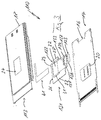
- Figure 1
- is an exploded, perspective view of a part of a plug-in card for electronic devices according to a first exemplary embodiment of the present invention,
- Figure 2
- is a perspective view of the part of the plug-in card assembled from the components shown in Figure 1,
- Figure 3
- is a diagram corresponding to Figure 1 but according to another exemplary embodiment of the present invention and
- Figure 4
- is a diagram corresponding to Figure 1 but according to a variant of Figure 3.
Claims (11)
- A plug-in card (10, 110, 210) for electronic devices of approximately oblong, flat formation with a housing comprising an upper and a lower, substantially half-shell-shaped housing part (13, 113, 213), a circuit board (16) accommodated in the housing, a contacting device (23, 123, 223) for a chip card (20) such as for example a SIM-, CCM-or the like card, and an accommodating means (21, 121, 221) for the chip card (20), characterised in that the chip card accommodating means (21, 121, 221) comprises a frame-like element (22, 122, 222) which is mounted on the laminar side of one of the housing parts (13, 113, 213) and is at least partially connected to an opening (24) in the laminar side of the relevant housing part (13, 113, 213) and in which the inserted chip card (20) can be accommodated, guided to the contacting device (23, 123, 223), and that the contacting device (23, 123, 223) is accommodated at one end of the frame-like element (22, 122, 222).
- A plug-in card according to Claim 1, characterised in that the frame-like element (22, 122, 222) is secured on the underneath of the relevant housing part (13, 113, 213).
- A plug-in card according to Claim 2, characterised in that the frame-like element (22, 122, 222) is adhesively attached to the underneath of the relevant housing part (13, 113, 213).
- A plug-in card according to Claim 1, characterised in that the frame-like element is inserted in the opening (24) of the relevant housing part (13, 113, 213), resting on the upper side at its edge.
- A plug-in card according to at least one of the preceding claims, characterised in that the frame-like element (22, 122, 222) comprises a feed ramp (32).
- A plug-in card according to Claim 5, characterised in that the ramp (32) of the frame-like element (22, 122, 222) is extended by a strip-shaped or laminar guide element (33).
- A plug-in card according to at least one of Claims 1 to 6, characterised in that the frame-like element (22, 122, 222) and a contact holder (36, 136, 236) of the contacting device (22, 122, 222) are of integral formation.
- A plug-in card according to Claim 7, characterised in that the frame-like element (22, 122, 222) is injection-moulded around the contacts (37) of the contacting device (23, 123, 223).
- A plug-in card according to at least one of Claims 1 to 6, characterised in that a contact holder (36, 136, 236) of the contacting device (23, 123, 223) is accommodated without play in a recess (34, 134, 234) of the frame-like element (22, 122, 222).
- A plug-in card according to Claim 9, characterised in that the contacting device (22, 122, 222) is attached via its contacts (37) to the circuit board (16) by a soldering connection.
- A plug-in card according to at least one of the preceding claims, characterised in that the contacting device (23, 123, 223) is arranged on the frame-like element (22, 122, 222) at a distance from the adjacent edge of the opening (24) in the relevant housing part (13, 113, 213) such as to permit the gripping of the surface of the inserted chip card (20) through the opening (24).
Applications Claiming Priority (2)
| Application Number | Priority Date | Filing Date | Title |
|---|---|---|---|
| DE19947162 | 1999-10-01 | ||
| DE19947162A DE19947162C1 (en) | 1999-10-01 | 1999-10-01 | Plug-in card for electronic equipment has frame element attached to housing part; chip card can be inserted into frame element to contacting device at end of frame element |
Publications (2)
| Publication Number | Publication Date |
|---|---|
| EP1089212A2 true EP1089212A2 (en) | 2001-04-04 |
| EP1089212A3 EP1089212A3 (en) | 2001-11-14 |
Family
ID=7924041
Family Applications (1)
| Application Number | Title | Priority Date | Filing Date |
|---|---|---|---|
| EP00118128A Withdrawn EP1089212A3 (en) | 1999-10-01 | 2000-08-28 | A plug-in card for electronic devices |
Country Status (6)
| Country | Link |
|---|---|
| US (1) | US6421246B1 (en) |
| EP (1) | EP1089212A3 (en) |
| JP (1) | JP2001134737A (en) |
| KR (1) | KR20010050660A (en) |
| DE (1) | DE19947162C1 (en) |
| TW (1) | TW563013B (en) |
Families Citing this family (25)
| Publication number | Priority date | Publication date | Assignee | Title |
|---|---|---|---|---|
| US7107378B1 (en) * | 2000-09-01 | 2006-09-12 | Sandisk Corporation | Cooperative interconnection and operation of a non-volatile memory card and an input-output card |
| US6783926B2 (en) * | 2001-09-15 | 2004-08-31 | Kenneth Reece | Circuit board IC card connector |
| DE20201237U1 (en) | 2002-01-28 | 2002-06-13 | Scm Microsystems Gmbh | Smart card reader |
| WO2003088021A2 (en) * | 2002-04-08 | 2003-10-23 | Socket Communications, Inc | Wireless enabled memory module |
| US7367503B2 (en) | 2002-11-13 | 2008-05-06 | Sandisk Corporation | Universal non-volatile memory card used with various different standard cards containing a memory controller |
| US8037229B2 (en) * | 2002-11-21 | 2011-10-11 | Sandisk Technologies Inc. | Combination non-volatile memory and input-output card with direct memory access |
| US20050055479A1 (en) * | 2002-11-21 | 2005-03-10 | Aviad Zer | Multi-module circuit card with inter-module direct memory access |
| DE10256716A1 (en) * | 2002-12-04 | 2004-06-24 | Siemens Ag | Smart card holder |
| DE10303740B4 (en) | 2003-01-30 | 2006-09-14 | Infineon Technologies Flash Gmbh & Co. Kg | Security memory card and manufacturing process |
| US7305535B2 (en) * | 2003-04-17 | 2007-12-04 | Sandisk Corporation | Memory cards including a standard security function |
| DE10321242B4 (en) | 2003-05-12 | 2008-04-10 | Siemens Ag | Card receiving device |
| US7209995B2 (en) * | 2003-12-09 | 2007-04-24 | Sandisk Corporation | Efficient connection between modules of removable electronic circuit cards |
| DE102006021023A1 (en) * | 2006-04-28 | 2007-10-31 | Würth Elektronik Rot am See GmbH & Co. KG | modules structure |
| US7572152B2 (en) * | 2007-06-27 | 2009-08-11 | Sandisk Il Ltd. | Memory interface card with SIM functions |
| CN101394716B (en) * | 2007-09-19 | 2011-11-16 | 深圳富泰宏精密工业有限公司 | Case component and portable electronic device having the case component |
| US8718541B2 (en) * | 2007-12-31 | 2014-05-06 | Intel Corporation | Techniques for optimal location and configuration of infrastructure relay nodes in wireless networks |
| CN101553100A (en) * | 2008-03-31 | 2009-10-07 | 深圳富泰宏精密工业有限公司 | Chip card fixing and clamping structure |
| US8462514B2 (en) | 2008-04-25 | 2013-06-11 | Apple Inc. | Compact ejectable component assemblies in electronic devices |
| CN101753644A (en) * | 2008-12-10 | 2010-06-23 | 深圳富泰宏精密工业有限公司 | Portable electronic device |
| TWM367443U (en) * | 2008-12-26 | 2009-10-21 | D & Amp C Technology Co Ltd | Electronic card for smart card to insert in |
| US8325486B2 (en) * | 2009-01-13 | 2012-12-04 | Dy 4 Systems Inc. | Tamper respondent module |
| US8654535B2 (en) * | 2012-03-08 | 2014-02-18 | Proconn Technology Co., Ltd. | Card holder |
| CN103579853A (en) * | 2012-08-06 | 2014-02-12 | 深圳富泰宏精密工业有限公司 | Chip card immobilizing device and electronic device applying chip card immobilizing device |
| USD707682S1 (en) * | 2012-12-05 | 2014-06-24 | Logomotion, S.R.O. | Memory card |
| US9195929B2 (en) * | 2013-08-05 | 2015-11-24 | A-Men Technology Corporation | Chip card assembling structure and method thereof |
Citations (4)
| Publication number | Priority date | Publication date | Assignee | Title |
|---|---|---|---|---|
| US5336877A (en) * | 1990-09-18 | 1994-08-09 | Amphenol-Tuchel Electronics Gmbh | Contacting device for standard chip card and SIM card |
| GB2299192A (en) * | 1995-03-20 | 1996-09-25 | Fujitsu Ltd | Portable telephones |
| EP0893777A2 (en) * | 1997-07-25 | 1999-01-27 | Nokia Mobile Phones Ltd. | A data card housing |
| US5877488A (en) * | 1996-04-22 | 1999-03-02 | Stocko Metallwarenfabriken Henkels Und Sohn Gmbh | Combination chip card reader |
Family Cites Families (2)
| Publication number | Priority date | Publication date | Assignee | Title |
|---|---|---|---|---|
| FR2747847B1 (en) * | 1996-04-18 | 1998-07-03 | Itt Composants Instr | ELECTRONIC CONNECTION BOX, TO A PERSONAL COMPUTER, EQUIPPED WITH A CONNECTOR FOR A CHIP CARD |
| DE19846366C2 (en) * | 1998-04-07 | 2000-07-27 | Itt Mfg Enterprises Inc | Plug-in card for electronic devices |
-
1999
- 1999-10-01 DE DE19947162A patent/DE19947162C1/en not_active Expired - Fee Related
-
2000
- 2000-08-28 EP EP00118128A patent/EP1089212A3/en not_active Withdrawn
- 2000-09-18 US US09/664,980 patent/US6421246B1/en not_active Expired - Fee Related
- 2000-09-21 JP JP2000286252A patent/JP2001134737A/en active Pending
- 2000-09-27 KR KR1020000056665A patent/KR20010050660A/en not_active Application Discontinuation
- 2000-09-30 TW TW089120393A patent/TW563013B/en active
Patent Citations (4)
| Publication number | Priority date | Publication date | Assignee | Title |
|---|---|---|---|---|
| US5336877A (en) * | 1990-09-18 | 1994-08-09 | Amphenol-Tuchel Electronics Gmbh | Contacting device for standard chip card and SIM card |
| GB2299192A (en) * | 1995-03-20 | 1996-09-25 | Fujitsu Ltd | Portable telephones |
| US5877488A (en) * | 1996-04-22 | 1999-03-02 | Stocko Metallwarenfabriken Henkels Und Sohn Gmbh | Combination chip card reader |
| EP0893777A2 (en) * | 1997-07-25 | 1999-01-27 | Nokia Mobile Phones Ltd. | A data card housing |
Also Published As
| Publication number | Publication date |
|---|---|
| KR20010050660A (en) | 2001-06-15 |
| TW563013B (en) | 2003-11-21 |
| US6421246B1 (en) | 2002-07-16 |
| JP2001134737A (en) | 2001-05-18 |
| EP1089212A3 (en) | 2001-11-14 |
| DE19947162C1 (en) | 2000-09-28 |
Similar Documents
| Publication | Publication Date | Title |
|---|---|---|
| EP1089212A2 (en) | A plug-in card for electronic devices | |
| US5877488A (en) | Combination chip card reader | |
| US6075706A (en) | PC card for receiving chip card | |
| KR100447683B1 (en) | Electrical connector for a contact-type smart card | |
| US5339222A (en) | Shielded printed circuit card holder | |
| JP3726215B2 (en) | Contact device for chip card device | |
| US7350705B1 (en) | Compact robust smart card reader | |
| US6842336B2 (en) | Portable electronic device with carrier plate | |
| US6398572B1 (en) | SIM (subscriber identity module) card holder with separate end stop | |
| JPH0836622A (en) | Reader of microcircuit card | |
| US6244902B1 (en) | Smart card reader for elevated placement relative to a printed circuit board | |
| EP1406204B1 (en) | Card holder for cellular phone | |
| JP4669969B2 (en) | Plug-in card for electronic devices | |
| US7372136B2 (en) | Chip card retaining mechanism | |
| US6508673B2 (en) | Low cost smart card reader, extension style, with wiping contacts | |
| US20020060248A1 (en) | Card reader connector | |
| KR20050055412A (en) | Socket for combined use of two different types of memory cards | |
| JP3629986B2 (en) | IC card loading device | |
| GB2360117A (en) | A SIM card holding device | |
| JP4707339B2 (en) | PC card | |
| TW200905993A (en) | Electrical card connector |
Legal Events
| Date | Code | Title | Description |
|---|---|---|---|
| PUAI | Public reference made under article 153(3) epc to a published international application that has entered the european phase |
Free format text: ORIGINAL CODE: 0009012 |
|
| AK | Designated contracting states |
Kind code of ref document: A2 Designated state(s): DE FR GB Kind code of ref document: A2 Designated state(s): AT BE CH CY DE DK ES FI FR GB GR IE IT LI LU MC NL PT SE |
|
| AX | Request for extension of the european patent |
Free format text: AL;LT;LV;MK;RO;SI |
|
| PUAL | Search report despatched |
Free format text: ORIGINAL CODE: 0009013 |
|
| AK | Designated contracting states |
Kind code of ref document: A3 Designated state(s): AT BE CH CY DE DK ES FI FR GB GR IE IT LI LU MC NL PT SE |
|
| AX | Request for extension of the european patent |
Free format text: AL;LT;LV;MK;RO;SI |
|
| 17P | Request for examination filed |
Effective date: 20020410 |
|
| AKX | Designation fees paid |
Free format text: DE FR GB |
|
| STAA | Information on the status of an ep patent application or granted ep patent |
Free format text: STATUS: THE APPLICATION IS DEEMED TO BE WITHDRAWN |
|
| 18D | Application deemed to be withdrawn |
Effective date: 20051215 |
|
| REG | Reference to a national code |
Ref country code: HK Ref legal event code: WD Ref document number: 1035421 Country of ref document: HK |