EP1098200B1 - Adjusting device for the planarization of probe sets of a probe card - Google Patents
Adjusting device for the planarization of probe sets of a probe card Download PDFInfo
- Publication number
- EP1098200B1 EP1098200B1 EP00123270A EP00123270A EP1098200B1 EP 1098200 B1 EP1098200 B1 EP 1098200B1 EP 00123270 A EP00123270 A EP 00123270A EP 00123270 A EP00123270 A EP 00123270A EP 1098200 B1 EP1098200 B1 EP 1098200B1
- Authority
- EP
- European Patent Office
- Prior art keywords
- needle
- card
- probe card
- adjusting device
- adjusting unit
- Prior art date
- Legal status (The legal status is an assumption and is not a legal conclusion. Google has not performed a legal analysis and makes no representation as to the accuracy of the status listed.)
- Expired - Lifetime
Links
Images

Classifications
-
- H—ELECTRICITY
- H01—ELECTRIC ELEMENTS
- H01L—SEMICONDUCTOR DEVICES NOT COVERED BY CLASS H10
- H01L22/00—Testing or measuring during manufacture or treatment; Reliability measurements, i.e. testing of parts without further processing to modify the parts as such; Structural arrangements therefor
-
- G—PHYSICS
- G01—MEASURING; TESTING
- G01R—MEASURING ELECTRIC VARIABLES; MEASURING MAGNETIC VARIABLES
- G01R31/00—Arrangements for testing electric properties; Arrangements for locating electric faults; Arrangements for electrical testing characterised by what is being tested not provided for elsewhere
- G01R31/28—Testing of electronic circuits, e.g. by signal tracer
- G01R31/2851—Testing of integrated circuits [IC]
- G01R31/2886—Features relating to contacting the IC under test, e.g. probe heads; chucks
- G01R31/2887—Features relating to contacting the IC under test, e.g. probe heads; chucks involving moving the probe head or the IC under test; docking stations
-
- G—PHYSICS
- G01—MEASURING; TESTING
- G01R—MEASURING ELECTRIC VARIABLES; MEASURING MAGNETIC VARIABLES
- G01R3/00—Apparatus or processes specially adapted for the manufacture or maintenance of measuring instruments, e.g. of probe tips
Definitions
- the present invention relates to a probe card adjusting device for planarizing needle sets of a probe card (also referred to as a probe card) with respect to a to be contacted wafer, in which the probe card with a as a contact interface to a test head serving board connected is.
- a probe card also referred to as a probe card
- US 5,861,859 describes an automatic planarization system for test cards, in which a test card is adjusted with respect to a wafer surface by first three tips of the test card, two of which are height-adjustable are aligned to the wafer surface.
- US-A-5 191 708 discloses a method of manufacturing a probe head for a semiconductor LSI monitor described. Probes go off a probe card via a wiring substrate.
- Needle sets of needle cards are known to be the electrical Connection between individual contact pads or pads of chips on the one hand and a test head ago, in order to improve the functionality to check the chips on the wafer.
- Needle sets need namely to the order of 1/4 micron accurate adjusted their respective assigned contact pads of the chips become.
- the probe card in addition to the static adjustment the probe card is also dynamic relative to the chips Components must be considered, for example by thermal expansion of the probe card during a Warming or cooling via a wafer holding device, also called "Chuck", are conditional.
- Other dynamic components are due to aging effects of the needle cards attributed to which the needle sets mostly are glued. But the dynamic components can as well very short time constants, such as shocks, to have.
- needle card glued needle sets are these not yet or only by subsequent bending everyone single needle adjusted, resulting in the required accuracy up to 1/4 micron a considerable cost and time means.
- the needle sets on so-called Spacetransformern Applied they can with the help of simple Adjusted screws, but with what the specified accuracy can hardly be reached.
- a probe card adjustment device to create with the the needle sets a probe card readily with respect to a to be contacted Wafers can be planarized.
- a probe card adjustment device of the type mentioned in the present invention achieved by that the probe card has a separate, dynamically operating Adjustment unit is connected to the board and that the adjustment unit via a sense line and an active line are connected to a control unit.
- this adjustment unit of at least one Piezo element constructed. But it can also be a variety of Piezo elements comprise in the edge region of the probe card attack at this.
- the planarity of the probe card can readily be in place and Place to be made by dynamic adjustment.
- The is called a needle card misalignment, for example, by Thermal expansion of the probe card or by short-term vibration caused, can be corrected easily. Due to the dynamic adjustability of the probe card let the parallelism between probe card and wafer Correct when contacting it beyond the edge of the wafer.
- the adjustment unit can move in directions that are essentially perpendicular to the spanned by the needle card surface Level, and / or in directions that are essentially lie in this plane, act.
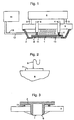
- Fig. 1 shows a probe card 1, by means of screws 4 between a board 3 and a window of a stiffening second is stored.
- the board 3 serves as a contact interface to a test head 5, with the help of test signals to individual needles 6 of the probe card 1 can be supplied.
- Fig. 2 shows the structure of such a needle 6, wherein here the needle 6 contacts a pad 7 on a chip 8 of a wafer.
- test head 5 The electrical connection between the test head 5 and the Board 3 is indicated by connecting buses 9, while between the board 3 and the individual needles 6 connecting wires 10 are guided.
- the screws 4 represent a mechanical adjustment unit, because by twisting parallelism between the probe card 1 and the surface of a contacted by the needles 6 Chips can be approximated.
- piezoelectric elements 11 provided, each via a sensor or Sense line 12 and an active line 13 with a control unit 14 are connected. Is through the piezo elements 11 a misalignment between the needles 6 of the probe card. 1 and the wafer surface is detected, this becomes misalignment reported via the sense line 12 to the computer 14. This will compensate for the misalignment necessary corrections to then appropriate Deliver signals via the active line 13 to the piezo elements 11.
- the lines 12, 13 form with the control unit 14 a Contact test loop, with the help of appropriate Dillatation or contraction of the piezo elements 11, the desired Adjustment can be made.
- the zero position of the probe card can be performed after a Adjustment be adjusted by means of screws 4, so that make the piezoelectric elements 11 only readjustments need.
- FIG. 3 shows a further embodiment of the invention, in which the probe card 1 with a set of needles 6 in one Window of a stiffening 2 is located.
- the Piezo elements 11 between this stiffener 2 and a Board 3 is arranged so that the adjustment alone on the Piezo elements 3 and not make additional screws 4 is.
- FIG. 3 in the same How the embodiment of Fig. 1 constructed: Again, the piezo elements 11 via corresponding lines (not shown separately in FIG. 3) with a control unit connected.
- Fig. 4 shows an embodiment in which an arrangement of several needle cards 1, which in a stiffening 2 acting solid frame are attached and laterally against this frame or against each other by piezoelectric elements 11th can be moved.
- Such laterally acting piezoelectric elements can easily also with the vertically acting piezoelectric elements of FIG. 1 and 3 are combined when, for example, in FIG. 1 between the stiffener 2 and the probe card 1 in appropriate Be attached.
Description
Die vorliegende Erfindung betrifft eine Nadelkarten-Justageeinrichtung zur Planarisierung von Nadelsätzen einer Nadelkarte (auch als Sondenkarte bezeichnet) in bezug auf einen zu kontaktierenden Wafer, bei der die Nadelkarte mit einer als Kontakt-Schnittstelle zu einem Testkopf dienenden Platine verbunden ist.The present invention relates to a probe card adjusting device for planarizing needle sets of a probe card (also referred to as a probe card) with respect to a to be contacted wafer, in which the probe card with a as a contact interface to a test head serving board connected is.
Aus der DE 25 44 735 A1 ist ein Prüfkopfträger bekannt, mit dessen Hilfe der Abstand zwischen einzelnen Prufköpfen, die Prüfspitzen tragen, eingestellt werden kann. Damit soll eine Anpassung der Prüfköpfe an verschiedene Schrumpfungen keramischer Substrate erreicht werden.From DE 25 44 735 A1 a Prüfkopfträger is known, with whose help is the distance between individual test heads, the Wear test probes, can be adjusted. This should be a Adaptation of the probes to different ceramic shrinkages Substrates can be achieved.
Weiterhin beschreibt die US 5,861,859 ein automatisches Planarisierungssystem für Prüfkarten, bei dem eine Prüfkarte bezüglich einer Waferoberfläche justiert wird, indem zuerst drei Spitzen der Prüfkarte, von denen zwei höhenvariabel sind, an der Waferoberfläche ausgerichtet werden.Furthermore, US 5,861,859 describes an automatic planarization system for test cards, in which a test card is adjusted with respect to a wafer surface by first three tips of the test card, two of which are height-adjustable are aligned to the wafer surface.
In US-A-5 191 708 ist ein Verfahren zur Herstellung eines Sondenkopfes für ein Halbleiter-LSI-überwachungsgerät beschrieben. Von einer Sondenkarte gehen über ein Verdrahtungssubstrat Sonden ab.US-A-5 191 708 discloses a method of manufacturing a probe head for a semiconductor LSI monitor described. Probes go off a probe card via a wiring substrate.
Nadelsätze von Nadelkarten stellen bekanntlich die elektrische Verbindung zwischen einzelnen Kontaktpads bzw. -kissen von Chips einerseits und einem Testkopf her, um so die Funktionsfähigkeit der Chips auf dem Wafer zu überprüfen. Dabei ist die Planarisierung der Nadelsätze der Nadelkarte in bezug auf den zu kontaktierenden Wafer bzw. die in diesem enthaltenen Chips mit zunehmender Anzahl der gleichzeitig zu kontaktierenden Chips immer aufwendiger. Die Nadelsätze müssen nämlich bis in die Größenordnung von 1/4 µm genau auf die ihnen jeweils zugeordneten Kontaktpads der Chips justiert werden. Needle sets of needle cards are known to be the electrical Connection between individual contact pads or pads of chips on the one hand and a test head ago, in order to improve the functionality to check the chips on the wafer. there is the planarization of the needle sets of the probe card with respect on the wafer to be contacted or contained in this Chips with increasing number of simultaneous too contacting chips increasingly expensive. Needle sets need namely to the order of 1/4 micron accurate adjusted their respective assigned contact pads of the chips become.
Dabei ist zu beachten, daß zusätzlich zu der statischen Justage der Nadelkarte relativ zu den Chips auch noch dynamische Komponenten berücksichtigt werden müssen, die beispielsweise durch Wärmeausdehnung der Nadelkarte während eines Aufwärmens bzw. Abkühlens über eine Wafer-Haltevorrichtung, auch "Chuck" genannt, bedingt sind. Andere dynamische Komponenten sind auf Alterungseffekte der Nadelkarten zurückzuführen, auf denen die Nadelsätze meistens verklebt sind. Die dynamischen Komponenten können aber auch sehr kurze Zeitkonstanten, wie beispielsweise bei Erschütterungen, haben.It should be noted that in addition to the static adjustment the probe card is also dynamic relative to the chips Components must be considered, for example by thermal expansion of the probe card during a Warming or cooling via a wafer holding device, also called "Chuck", are conditional. Other dynamic components are due to aging effects of the needle cards attributed to which the needle sets mostly are glued. But the dynamic components can as well very short time constants, such as shocks, to have.
Bei auf der Nadelkarte verklebten Nadelsätzen werden diese bisher nicht oder nur durch nachträgliches Verbiegen jeder einzelnen Nadel justiert, was bei der geforderten Genauigkeit bis zu 1/4 µm einen erheblichen Kosten- und Zeitaufwand bedeutet. Sind die Nadelsätze auf sogenannten Spacetransformern aufgebracht, so können sie mit Hilfe von einfachen Schrauben justiert werden, womit aber die angegebene Genauigkeit kaum zu erreichen ist.In the needle card glued needle sets are these not yet or only by subsequent bending everyone single needle adjusted, resulting in the required accuracy up to 1/4 micron a considerable cost and time means. Are the needle sets on so-called Spacetransformern Applied, they can with the help of simple Adjusted screws, but with what the specified accuracy can hardly be reached.
Es ist daher Aufgabe der vorliegenden Erfindung, eine Nadelkarten-Justageeinrichtung zu schaffen, mit der die Nadelsätze einer Nadelkarte ohne weiteres in bezug auf einen zu kontaktierenden Wafer planarisiert werden können.It is therefore an object of the present invention, a probe card adjustment device to create with the the needle sets a probe card readily with respect to a to be contacted Wafers can be planarized.
Diese Aufgabe wird bei einer Nadelkarten-Justageeinrichtung der eingangs genannten Art erfindungsgemäß dadurch gelöst, daß die Nadelkarte über eine gesonderte, dynamisch arbeitende Justageeinheit mit der Platine verbunden ist und daß die Justageeinheit über eine Sense-Leitung und eine Aktivleitung mit einer Steuereinheit verbunden sind. In bevorzugter Weise ist diese Justageeinheit aus wenigstens einem Piezoelement aufgebaut. Sie kann aber auch eine Vielzahl von Piezoelementen umfassen, die im Randbereich der Nadelkarte an dieser angreifen. This object is achieved with a probe card adjustment device of the type mentioned in the present invention achieved by that the probe card has a separate, dynamically operating Adjustment unit is connected to the board and that the adjustment unit via a sense line and an active line are connected to a control unit. In preferred Way is this adjustment unit of at least one Piezo element constructed. But it can also be a variety of Piezo elements comprise in the edge region of the probe card attack at this.
Mit der erfindungsgemäßen Nadelkarten-Justageeinrichtung kann die Planarität der Nadelkarte ohne weiteres an Ort und Stelle durch dynamische Justage hergestellt werden. Das heißt, eine Nadelkarten-Dejustage, die beispielsweise durch Wärmeausdehnung der Nadelkarte oder durch kurzzeitige Erschütterung hervorgerufen ist, läßt sich ohne weiteres korrigieren. Infolge der dynamischen Einstellbarkeit der Nadelkarte laßt sich die Parallelität zwischen Nadelkarte und Wafer bei dessen Kontaktierung über den Waferrand hinaus korrigieren.With the needle card adjustment device according to the invention The planarity of the probe card can readily be in place and Place to be made by dynamic adjustment. The is called a needle card misalignment, for example, by Thermal expansion of the probe card or by short-term vibration caused, can be corrected easily. Due to the dynamic adjustability of the probe card let the parallelism between probe card and wafer Correct when contacting it beyond the edge of the wafer.
Da mit der gesonderten, dynamisch arbeitenden Justageeinheit, über die die Nadelkarte mit der Platine verbunden ist, ohne weiteres auch dynamische Effekte korrigierbar sind, entfällt jeglicher Bedarf für zusätzliche Einstelleinrichtungen. Auch kann mit Hilfe einer Kontakttestschleife, d.h. einem Programm zur Verifikation des Kontaktes jeder Nadel zu einem zugehörigen Pad, die Justage vorgenommen werden.Because with the separate, dynamically adjusting unit, via which the probe card is connected to the board, readily dynamic effects can be corrected, eliminates any need for additional adjusters. Also, with the aid of a contact test loop, i. a program for verifying the contact of each needle an associated pad, the adjustment be made.
Die Justageeinheit kann in Richtungen, die im wesentlichen senkrecht zu der durch die Nadelkarten-Oberfläche aufgespannten Ebene sind, und/oder in Richtungen, die im wesentlichen in dieser Ebene liegen, wirken.The adjustment unit can move in directions that are essentially perpendicular to the spanned by the needle card surface Level, and / or in directions that are essentially lie in this plane, act.
Durch den Aufbau der Justageeinheit aus insbesondere Piezoelementen laßt sich deren Einstellbarkeit mit hoher Präzision realisieren.Due to the structure of the adjustment unit in particular piezoelectric elements let their adjustability with high precision realize.
Nachfolgend wird die Erfindung anhand der Zeichnungen näher erläutert. Es zeigen:
- Fig. 1
- eine schematische Seitenansicht einer Nadelkarten-Justageeinrichtung nach einem ersten Ausführungsbeispiel der Erfindung,
- Fig. 2
- eine schematische Darstellung einer Nadel, die ein Pad auf einem Chip kontaktiert,
- Fig. 3
- eine schematische Seitenansicht einer Nadelkarten-Justageeinheit nach einem zweiten Ausführungsbeispiel der Erfindung und
- Fig. 4
- eine Draufsicht auf mehrere Nadelkartensätze in einer Nadelkarten-Justageeinheit nach einem vierten Ausführungsbeispiel der Erfindung.
- Fig. 1
- 1 is a schematic side view of a needle card adjusting device according to a first embodiment of the invention,
- Fig. 2
- a schematic representation of a needle contacting a pad on a chip,
- Fig. 3
- a schematic side view of a needle card adjusting unit according to a second embodiment of the invention and
- Fig. 4
- a plan view of a plurality of needle card sets in a probe card adjustment unit according to a fourth embodiment of the invention.
Fig. 1 zeigt eine Nadelkarte 1, die mittels Schrauben 4 zwischen
einer Platine 3 und einem Fenster einer Versteifung 2
gelagert ist. Die Platine 3 dient dabei als Kontakt-Schnittstelle
zu einem Testkopf 5, mit dessen Hilfe Testsignale zu
einzelnen Nadeln 6 der Nadelkarte 1 geliefert werden können.Fig. 1 shows a
Fig. 2 zeigt den Aufbau einer solchen Nadel 6, wobei hier
die Nadel 6 ein Pad 7 auf einem Chip 8 eines Wafers kontaktiert.Fig. 2 shows the structure of such a
Die elektrische Verbindung zwischen dem Testkopf 5 und der
Platine 3 ist durch Verbindungsbusse 9 angedeutet, während
zwischen der Platine 3 und den einzelnen Nadeln 6 Verbindungsdrähte
10 geführt sind.The electrical connection between the
Die Schrauben 4 stellen eine mechanische Justageeinheit dar,
da durch deren Verdrehen Parallelität zwischen der Nadelkarte
1 und der Oberfläche eines durch die Nadeln 6 kontaktierten
Chips näherungsweise bewirkt werden kann.The
Erfindungsgemäß sind zusätzlich zu den Schrauben 4 noch Piezoelemente
11 vorgesehen, die jeweils über eine Fühler- bzw.
Sense-Leitung 12 und eine Aktivleitung 13 mit einer Steuereinheit
14 verbunden sind. Wird durch die Piezoelemente 11
eine Fehlausrichtung zwischen den Nadeln 6 der Nadelkarte 1
und der Waferoberfläche festgestellt, so wird diese Fehlausrichtung
über die Sense-Leitung 12 an den Rechner 14 gemeldet.
In diesem werden die zum Ausgleich der Fehlausrichtung
notwendigen Korrekturen berechnet, um sodann entsprechende
Signale über die Aktivleitung 13 an die Piezoelemente 11 abzugeben.According to the invention, in addition to the
Selbstverständlich sind alle Piezoelemente 11 über entsprechende
Leitungen 12, 13 mit der Steuereinheit 14 verbunden,
obwohl dies in Fig. 1 zur besseren Übersichtlichkeit nur für
ein Piezoelement 11 gezeigt ist.Of course, all the
Anstelle von Piezoelementen können auch andere, eine dynamische Justage ermöglichende Bauteile verwendet werden.Instead of piezo elements, others, a dynamic Adjustment enabling components can be used.
Die Leitungen 12, 13 bilden mit der Steuereinheit 14 eine
Kontakttestschleife, mit deren Hilfe durch entsprechende
Dillatation bzw. Kontraktion der Piezoelemente 11 die gewünschte
Justage vorgenommen werden kann.The
Die Nullposition der Nadelkarte kann nach einer durchgeführten
Justage mittels der Schrauben 4 eingestellt werden, so
daß die Piezoelemente 11 nur noch Nachjustierungen vorzunehmen
brauchen.The zero position of the probe card can be performed after a
Adjustment be adjusted by means of
Fig. 3 zeigt ein weiteres Ausführungsbeispiel der Erfindung,
bei dem die Nadelkarte 1 mit einem Satz aus Nadeln 6 in einem
Fenster einer Versteifung 2 gelegen ist. Hier sind die
Piezoelemente 11 zwischen dieser Versteifung 2 und einer
Platine 3 angeordnet, so daß die Justage allein über die
Piezoelemente 3 und nicht über zusätzliche Schrauben 4 vorzunehmen
ist.3 shows a further embodiment of the invention,
in which the
Im übrigen ist das Ausführungsbeispiel der Fig. 3 in gleicher
Weise wie das Ausführungsbeispiel der Fig. 1 aufgebaut:
auch hier sind die Piezoelemente 11 über entsprechende Leitungen
(in Fig. 3 nicht gesondert gezeigt) mit einer Steuereinheit
verbunden. Incidentally, the embodiment of FIG. 3 in the same
How the embodiment of Fig. 1 constructed:
Again, the
Fig. 4 zeigt ein Ausführungsbeispiel, bei dem eine Anordnung
von mehreren Nadelkarten 1, die in einem als Versteifung 2
wirkenden festen Rahmen angebracht sind und lateral gegen
diesen Rahmen bzw. gegen einander durch Piezoelemente 11
verschoben werden können.Fig. 4 shows an embodiment in which an arrangement
of
Solche lateral wirkende Piezoelemente können ohne weiteres
auch mit den vertikal wirkenden Piezoelementen der Fig. 1
und 3 kombiniert werden, wenn sie beispielsweise in Fig. 1
zwischen der Versteifung 2 und der Nadelkarte 1 in geeigneter
Weise angebracht werden.Such laterally acting piezoelectric elements can easily
also with the vertically acting piezoelectric elements of FIG. 1
and 3 are combined when, for example, in FIG. 1
between the
Claims (5)
- Needle-card adjusting device for planarizing needle sets (6) on a needle card (1) in relation to a wafer (8) with which contact is to be made, in which the needle card (1) is connected to a circuit board (3) used as a contact interface to a test head (5), characterized in thatthe needle card (1) is connected to the circuit board (3) via a separate, dynamically operating adjusting unit (4; 11), andthe adjusting unit (4, 11) is connected to a control unit (14) via a sense line (12) and an active line (13).
- Needle-card adjusting device according to Claim 1, characterized in that the adjusting unit is constructed from at least one piezoelectric element (11).
- Needle-card adjusting device according to Claim 2, characterized in that the adjusting unit has a multiplicity of piezoelectric elements (11), which act on the needle card (1) in the edge region thereof.
- Needle-card adjusting device according to one of Claims 1 to 3, characterized in that a stiffening means (2) is additionally provided between the needle card (1) and the adjusting unit (11).
- Needle-card adjusting device according to one of Claims 1 to 4, characterized in that the adjusting unit (4; 11) acts in directions which are essentially perpendicular to the plane covered by the needle-card surface and/or in directions which are essentially in this plane.
Applications Claiming Priority (2)
| Application Number | Priority Date | Filing Date | Title |
|---|---|---|---|
| DE19952943 | 1999-11-03 | ||
| DE19952943A DE19952943C2 (en) | 1999-11-03 | 1999-11-03 | Needle card adjustment device for the planarization of needle sets of a needle card |
Publications (3)
| Publication Number | Publication Date |
|---|---|
| EP1098200A2 EP1098200A2 (en) | 2001-05-09 |
| EP1098200A3 EP1098200A3 (en) | 2003-08-13 |
| EP1098200B1 true EP1098200B1 (en) | 2005-07-06 |
Family
ID=7927803
Family Applications (1)
| Application Number | Title | Priority Date | Filing Date |
|---|---|---|---|
| EP00123270A Expired - Lifetime EP1098200B1 (en) | 1999-11-03 | 2000-10-26 | Adjusting device for the planarization of probe sets of a probe card |
Country Status (7)
| Country | Link |
|---|---|
| US (1) | US6674627B1 (en) |
| EP (1) | EP1098200B1 (en) |
| JP (1) | JP2001189354A (en) |
| KR (1) | KR20010051378A (en) |
| CN (1) | CN1196935C (en) |
| DE (2) | DE19952943C2 (en) |
| TW (1) | TW548411B (en) |
Cited By (4)
| Publication number | Priority date | Publication date | Assignee | Title |
|---|---|---|---|---|
| US7737709B2 (en) | 2000-03-17 | 2010-06-15 | Formfactor, Inc. | Methods for planarizing a semiconductor contactor |
| US7948252B2 (en) | 2001-07-11 | 2011-05-24 | Formfactor, Inc. | Multilayered probe card |
| US8373428B2 (en) | 1993-11-16 | 2013-02-12 | Formfactor, Inc. | Probe card assembly and kit, and methods of making same |
| US8485418B2 (en) | 1995-05-26 | 2013-07-16 | Formfactor, Inc. | Method of wirebonding that utilizes a gas flow within a capillary from which a wire is played out |
Families Citing this family (20)
| Publication number | Priority date | Publication date | Assignee | Title |
|---|---|---|---|---|
| DE10056882C2 (en) | 2000-11-16 | 2003-06-05 | Infineon Technologies Ag | Method for calibrating a test system for semiconductor components and test substrate |
| US6972578B2 (en) | 2001-11-02 | 2005-12-06 | Formfactor, Inc. | Method and system for compensating thermally induced motion of probe cards |
| US7071714B2 (en) | 2001-11-02 | 2006-07-04 | Formfactor, Inc. | Method and system for compensating for thermally induced motion of probe cards |
| JP2003222654A (en) | 2002-01-30 | 2003-08-08 | Tokyo Electron Ltd | Probe device |
| US20050110004A1 (en) * | 2003-11-24 | 2005-05-26 | International Business Machines Corporation | Magnetic tunnel junction with improved tunneling magneto-resistance |
| US7071715B2 (en) * | 2004-01-16 | 2006-07-04 | Formfactor, Inc. | Probe card configuration for low mechanical flexural strength electrical routing substrates |
| DE102004023987B4 (en) * | 2004-05-14 | 2008-06-19 | Feinmetall Gmbh | Electrical testing device |
| US7471094B2 (en) * | 2005-06-24 | 2008-12-30 | Formfactor, Inc. | Method and apparatus for adjusting a multi-substrate probe structure |
| US7671614B2 (en) * | 2005-12-02 | 2010-03-02 | Formfactor, Inc. | Apparatus and method for adjusting an orientation of probes |
| US20070176615A1 (en) * | 2006-01-27 | 2007-08-02 | Xandex, Inc. | Active probe contact array management |
| DE102006018474A1 (en) * | 2006-04-19 | 2007-10-25 | Infineon Technologies Ag | Test device for semiconductor elements on a semiconductor wafer and a test method using the test device |
| DE102007054187B4 (en) * | 2006-11-27 | 2018-08-02 | Feinmetall Gmbh | Contacting device for contacting an electrical test specimen to be tested and corresponding contacting method |
| JP5190195B2 (en) * | 2006-11-29 | 2013-04-24 | 株式会社日本マイクロニクス | Electrical connection device |
| JP2008134170A (en) * | 2006-11-29 | 2008-06-12 | Micronics Japan Co Ltd | Electrically connecting device |
| KR100790817B1 (en) * | 2006-12-06 | 2008-01-03 | 삼성전자주식회사 | System for managing semiconductor divice manufacturing equipment |
| US7764076B2 (en) * | 2007-02-20 | 2010-07-27 | Centipede Systems, Inc. | Method and apparatus for aligning and/or leveling a test head |
| JP5643476B2 (en) * | 2008-04-16 | 2014-12-17 | 日本電子材料株式会社 | Double elastic mechanism probe card |
| US8004296B2 (en) * | 2008-08-19 | 2011-08-23 | Centipede Systems, Inc. | Probe head apparatus for testing semiconductors |
| KR101645167B1 (en) * | 2010-06-01 | 2016-08-03 | 리노공업주식회사 | A pitch transformer and a probe card including the same |
| CN104858769B (en) * | 2014-02-26 | 2018-12-18 | 盛美半导体设备(上海)有限公司 | Relative ranging device and method |
Family Cites Families (12)
| Publication number | Priority date | Publication date | Assignee | Title |
|---|---|---|---|---|
| US3963985A (en) | 1974-12-12 | 1976-06-15 | International Business Machines Corporation | Probe device having probe heads and method of adjusting distances between probe heads |
| GB2094479B (en) * | 1978-01-30 | 1983-03-16 | Texas Instruments Inc | Determining probe contact in testing integrated circuits |
| JP2928592B2 (en) * | 1990-06-20 | 1999-08-03 | 株式会社日立製作所 | Method of manufacturing probe head for semiconductor LSI inspection apparatus and inspection apparatus |
| JP3219844B2 (en) * | 1992-06-01 | 2001-10-15 | 東京エレクトロン株式会社 | Probe device |
| US5422574A (en) * | 1993-01-14 | 1995-06-06 | Probe Technology Corporation | Large scale protrusion membrane for semiconductor devices under test with very high pin counts |
| US5974662A (en) * | 1993-11-16 | 1999-11-02 | Formfactor, Inc. | Method of planarizing tips of probe elements of a probe card assembly |
| KR100248569B1 (en) * | 1993-12-22 | 2000-03-15 | 히가시 데쓰로 | Probe system |
| JPH0883825A (en) * | 1994-09-09 | 1996-03-26 | Tokyo Electron Ltd | Probe equipment |
| JP3838381B2 (en) * | 1995-11-22 | 2006-10-25 | 株式会社アドバンテスト | Probe card |
| US5861759A (en) * | 1997-01-29 | 1999-01-19 | Tokyo Electron Limited | Automatic probe card planarization system |
| JPH1123615A (en) * | 1997-05-09 | 1999-01-29 | Hitachi Ltd | Connector and inspection system |
| JP3090132B2 (en) * | 1998-12-18 | 2000-09-18 | 株式会社日立製作所 | Method of manufacturing probe head |
-
1999
- 1999-11-03 DE DE19952943A patent/DE19952943C2/en not_active Expired - Fee Related
-
2000
- 2000-10-26 EP EP00123270A patent/EP1098200B1/en not_active Expired - Lifetime
- 2000-10-26 DE DE50010659T patent/DE50010659D1/en not_active Expired - Fee Related
- 2000-11-01 JP JP2000334568A patent/JP2001189354A/en active Pending
- 2000-11-01 KR KR1020000064569A patent/KR20010051378A/en not_active Application Discontinuation
- 2000-11-02 TW TW089123085A patent/TW548411B/en not_active IP Right Cessation
- 2000-11-03 CN CNB001355236A patent/CN1196935C/en not_active Expired - Fee Related
- 2000-11-03 US US09/705,599 patent/US6674627B1/en not_active Expired - Lifetime
Cited By (5)
| Publication number | Priority date | Publication date | Assignee | Title |
|---|---|---|---|---|
| US8373428B2 (en) | 1993-11-16 | 2013-02-12 | Formfactor, Inc. | Probe card assembly and kit, and methods of making same |
| US8485418B2 (en) | 1995-05-26 | 2013-07-16 | Formfactor, Inc. | Method of wirebonding that utilizes a gas flow within a capillary from which a wire is played out |
| US7737709B2 (en) | 2000-03-17 | 2010-06-15 | Formfactor, Inc. | Methods for planarizing a semiconductor contactor |
| US8427183B2 (en) | 2000-03-17 | 2013-04-23 | Formfactor, Inc. | Probe card assembly having an actuator for bending the probe substrate |
| US7948252B2 (en) | 2001-07-11 | 2011-05-24 | Formfactor, Inc. | Multilayered probe card |
Also Published As
| Publication number | Publication date |
|---|---|
| EP1098200A2 (en) | 2001-05-09 |
| DE19952943C2 (en) | 2003-07-03 |
| DE19952943A1 (en) | 2001-06-13 |
| US6674627B1 (en) | 2004-01-06 |
| JP2001189354A (en) | 2001-07-10 |
| TW548411B (en) | 2003-08-21 |
| EP1098200A3 (en) | 2003-08-13 |
| DE50010659D1 (en) | 2005-08-11 |
| CN1196935C (en) | 2005-04-13 |
| KR20010051378A (en) | 2001-06-25 |
| CN1300943A (en) | 2001-06-27 |
Similar Documents
| Publication | Publication Date | Title |
|---|---|---|
| EP1098200B1 (en) | Adjusting device for the planarization of probe sets of a probe card | |
| EP0369112B1 (en) | Adapter for electronic test devices for printed-circuit boards and the like | |
| DE69926241T2 (en) | PCB CONNECTING DEVICE AND METHOD OF MANUFACTURING | |
| DE19648475B4 (en) | Contact structure, test cards and manufacturing process | |
| DE4133769C2 (en) | Mounting system for coupling test plates for the recording of electronic components to be tested to a semiconductor test system | |
| EP1152368B1 (en) | Chip card | |
| DE102007039728B4 (en) | probe assembly | |
| WO2005091366A2 (en) | Semiconductor module comprising a coupling substrate and associated production method | |
| DE19835840B4 (en) | Manufacturing method for a semiconductor chip | |
| EP0283545A1 (en) | Contact-pins arrangement for the electrical contacting of a test device with circular contact surfaces of a test sample | |
| WO2000079589A1 (en) | Electronic component with flexible contact structures and method for the production of said component | |
| DE19507127A1 (en) | Adapter system for component boards, to be used in a test facility | |
| EP1111397B1 (en) | Means for testing chips using a printed circuit | |
| DE2903517A1 (en) | PROBE AND TEST ARRANGEMENT EQUIPPED WITH IT AND THE TEST PROCEDURE TO BE CARRIED OUT WITH IT | |
| DE102006008454B4 (en) | Pad structure, pad layout structure, semiconductor device, and pad layout method | |
| WO2000041241A1 (en) | Vertically integrated semiconductor system | |
| DE112005003731B4 (en) | Method for mounting an electrical connection device | |
| DE10126610B4 (en) | Memory module and method for testing a semiconductor chip | |
| EP0005727B1 (en) | Sensing probe for determining location of conductive spots | |
| EP1128424A2 (en) | Test structure close to integrated semiconductor | |
| WO1998012747A1 (en) | Integrated circuit with housing accommodating the latter | |
| DE10216823A1 (en) | Semiconductor module, semiconductor assembly and method for producing a semiconductor module | |
| DE10228152A1 (en) | Self-adhesive flexible repair circuit | |
| EP1772045B1 (en) | Positioning device provided with a linearly displaceable positioning unit | |
| DE10106836B4 (en) | Integrated circuit arrangement of a flat substrate |
Legal Events
| Date | Code | Title | Description |
|---|---|---|---|
| PUAI | Public reference made under article 153(3) epc to a published international application that has entered the european phase |
Free format text: ORIGINAL CODE: 0009012 |
|
| AK | Designated contracting states |
Kind code of ref document: A2 Designated state(s): AT BE CH CY DE DK ES FI FR GB GR IE IT LI LU MC NL PT SE |
|
| AX | Request for extension of the european patent |
Free format text: AL;LT;LV;MK;RO;SI |
|
| PUAL | Search report despatched |
Free format text: ORIGINAL CODE: 0009013 |
|
| AK | Designated contracting states |
Designated state(s): AT BE CH CY DE DK ES FI FR GB GR IE IT LI LU MC NL PT SE |
|
| AX | Request for extension of the european patent |
Extension state: AL LT LV MK RO SI |
|
| 17P | Request for examination filed |
Effective date: 20040127 |
|
| AKX | Designation fees paid |
Designated state(s): DE FR GB IE IT NL |
|
| 17Q | First examination report despatched |
Effective date: 20040706 |
|
| GRAP | Despatch of communication of intention to grant a patent |
Free format text: ORIGINAL CODE: EPIDOSNIGR1 |
|
| GRAS | Grant fee paid |
Free format text: ORIGINAL CODE: EPIDOSNIGR3 |
|
| GRAA | (expected) grant |
Free format text: ORIGINAL CODE: 0009210 |
|
| AK | Designated contracting states |
Kind code of ref document: B1 Designated state(s): DE FR GB IE IT NL |
|
| REG | Reference to a national code |
Ref country code: GB Ref legal event code: FG4D Free format text: NOT ENGLISH |
|
| REG | Reference to a national code |
Ref country code: IE Ref legal event code: FG4D Free format text: LANGUAGE OF EP DOCUMENT: GERMAN |
|
| REF | Corresponds to: |
Ref document number: 50010659 Country of ref document: DE Date of ref document: 20050811 Kind code of ref document: P |
|
| GBT | Gb: translation of ep patent filed (gb section 77(6)(a)/1977) |
Effective date: 20050914 |
|
| PGFP | Annual fee paid to national office [announced via postgrant information from national office to epo] |
Ref country code: NL Payment date: 20051013 Year of fee payment: 6 |
|
| ET | Fr: translation filed | ||
| PLBE | No opposition filed within time limit |
Free format text: ORIGINAL CODE: 0009261 |
|
| STAA | Information on the status of an ep patent application or granted ep patent |
Free format text: STATUS: NO OPPOSITION FILED WITHIN TIME LIMIT |
|
| 26N | No opposition filed |
Effective date: 20060407 |
|
| PG25 | Lapsed in a contracting state [announced via postgrant information from national office to epo] |
Ref country code: NL Free format text: LAPSE BECAUSE OF NON-PAYMENT OF DUE FEES Effective date: 20070501 |
|
| NLV4 | Nl: lapsed or anulled due to non-payment of the annual fee |
Effective date: 20070501 |
|
| PGFP | Annual fee paid to national office [announced via postgrant information from national office to epo] |
Ref country code: IT Payment date: 20071024 Year of fee payment: 8 |
|
| PGFP | Annual fee paid to national office [announced via postgrant information from national office to epo] |
Ref country code: FR Payment date: 20071016 Year of fee payment: 8 Ref country code: GB Payment date: 20071023 Year of fee payment: 8 |
|
| PGFP | Annual fee paid to national office [announced via postgrant information from national office to epo] |
Ref country code: DE Payment date: 20071211 Year of fee payment: 8 |
|
| GBPC | Gb: european patent ceased through non-payment of renewal fee |
Effective date: 20081026 |
|
| REG | Reference to a national code |
Ref country code: IE Ref legal event code: MM4A |
|
| REG | Reference to a national code |
Ref country code: FR Ref legal event code: ST Effective date: 20090630 |
|
| PG25 | Lapsed in a contracting state [announced via postgrant information from national office to epo] |
Ref country code: DE Free format text: LAPSE BECAUSE OF NON-PAYMENT OF DUE FEES Effective date: 20090501 Ref country code: IT Free format text: LAPSE BECAUSE OF NON-PAYMENT OF DUE FEES Effective date: 20081026 |
|
| PGFP | Annual fee paid to national office [announced via postgrant information from national office to epo] |
Ref country code: IE Payment date: 20071023 Year of fee payment: 8 |
|
| PG25 | Lapsed in a contracting state [announced via postgrant information from national office to epo] |
Ref country code: IE Free format text: LAPSE BECAUSE OF NON-PAYMENT OF DUE FEES Effective date: 20081027 Ref country code: FR Free format text: LAPSE BECAUSE OF NON-PAYMENT OF DUE FEES Effective date: 20081031 |
|
| PG25 | Lapsed in a contracting state [announced via postgrant information from national office to epo] |
Ref country code: GB Free format text: LAPSE BECAUSE OF NON-PAYMENT OF DUE FEES Effective date: 20081026 |