EP1104119A2 - Transmitter adjusting output power - Google Patents
Transmitter adjusting output power Download PDFInfo
- Publication number
- EP1104119A2 EP1104119A2 EP00309464A EP00309464A EP1104119A2 EP 1104119 A2 EP1104119 A2 EP 1104119A2 EP 00309464 A EP00309464 A EP 00309464A EP 00309464 A EP00309464 A EP 00309464A EP 1104119 A2 EP1104119 A2 EP 1104119A2
- Authority
- EP
- European Patent Office
- Prior art keywords
- gain
- amplifying stage
- variable
- signal
- transmit signal
- Prior art date
- Legal status (The legal status is an assumption and is not a legal conclusion. Google has not performed a legal analysis and makes no representation as to the accuracy of the status listed.)
- Granted
Links
Images

Classifications
-
- H—ELECTRICITY
- H04—ELECTRIC COMMUNICATION TECHNIQUE
- H04B—TRANSMISSION
- H04B1/00—Details of transmission systems, not covered by a single one of groups H04B3/00 - H04B13/00; Details of transmission systems not characterised by the medium used for transmission
- H04B1/02—Transmitters
-
- H—ELECTRICITY
- H04—ELECTRIC COMMUNICATION TECHNIQUE
- H04W—WIRELESS COMMUNICATION NETWORKS
- H04W52/00—Power management, e.g. TPC [Transmission Power Control], power saving or power classes
- H04W52/04—TPC
- H04W52/52—TPC using AGC [Automatic Gain Control] circuits or amplifiers
Definitions
- the present invention relates to a transmitter adjusting output power, and more particularly to a transmitter which, driven by a battery as in the handset of a mobile telephone, adjusts output power so as to minimize the exhaustion of the power source battery when adjusting the output power of transmit signals.
- a cordless mobile telephone when communicating with another mobile telephone, is subject to fluctuations in the field intensity of the receive wave reaching each mobile telephone depending on the distance between the calling party's mobile telephone and the corresponding telephone relaying base and the state of wave transmission in-between as well as the distance between the other party's mobile telephone and the corresponding telephone relaying base and the state of wave transmission in-between.
- the link with the other party may be so much affected by noise and the like that satisfactory communication is made difficult or sometimes even impossible.
- the field intensity of the receive wave reaching the calling party's mobile telephone is strong, the transmission/reception of the wave may be taking place at a signal level which is higher than a necessary signal level, and this is not necessarily desirable because the exhaustion of the power source battery of the mobile telephone would increase correspondingly.
- the field strength of the receive wave should be detected and, if the detected field strength is relatively large, the signal gain of the transmitter should be adjusted according to the relative level of the detected field strength to reduce the level of the transmit signal from the transmitter. If the detected field strength is relatively weak, the signal gain of the transmitter should be adjusted according to the relative level of the detected field strength to enhance the level of the transmit signal from the transmitter.
- the field strength of the wave received by each other's mobile telephone can be regulated to a standard level, thereby enabling the two mobile telephones to communicate satisfactorily and prevent both mobile telephones from suffering unnecessary exhaustion of their respective power source batteries.
- Adjusting means known to be available according to the prior art for signal gains of transmitters in mobile telephone include first gain adjusting means which fixes the signal gain in the power amplifying stage and makes controllable the signal gain in the drive amplifying stage with a gain control voltage to adjust the level of the transmit signal as required, and second gain adjusting means which fixes the signal gain in the drive amplifying stage and makes controllable the signal gain in the power amplifying stage with a gain control voltage to adjust the level of the transmit signal as required.
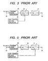
- Fig. 3 is a block diagram illustrating the configuration of essential parts of a transmitter using a first gain adjusting means in a known mobile telephone.
- this transmitter is provided with a fixed-gain power amplifying stage (PA) 31, a variable-gain drive amplifying stage (DA) 32, a transmit signal generator 33, a gain control voltage generator 34, a transmit signal output terminal 35 and a transmit data (TX data) input terminal 36.
- PA fixed-gain power amplifying stage
- DA variable-gain drive amplifying stage
- TX data transmit data input terminal 36
- the transmit signal generator 33 the input terminal is connected to the transmit data input terminal 36 and the output terminal is connected to the input terminal of the variable-gain drive amplifying stage 32.
- the control terminal is connected to the output terminal of the gain control voltage generator 34 and the output terminal is connected to the input terminal of the fixed-gain power amplifying stage 31.
- the output terminal is connected to the transmit signal output terminal 35.
- the transmit signal generator 33 forms a carrier frequency, and modulates the formed carrier frequency with transmit data (TX data) supplied to the transmit data input terminal 36 to generate a transmit signal, and the generated transmit signal is supplied to the variable-gain drive amplifying stage 32 that follows.
- the gain control voltage generator 34 generates a gain control voltage corresponding to the level of the receive signal that has been received (the field strength of the receive wave), and the gain control voltage so obtained is supplied to the variable-gain drive amplifying stage 32.
- the transmit signal output terminal 35 is connected to a transmission antenna (not shown in Fig. 3).
- the transmitter using the first gain adjusting means having the above-described configuration operates in the following manner.
- the controller detects a receive signal level representing the field strength of the receive wave. If the detected receive signal level is relatively low, the gain control voltage generator 34 generates a gain control signal to increase the signal gain of the variable-gain drive amplifying stage 32 according to the relative level of the receive signal level, and supplies it to the variable-gain drive amplifying stage 32.
- the gain control voltage generator 34 If the detected receive signal level is relatively high, the gain control voltage generator 34 generates a gain control signal to reduce the signal gain of the variable-gain drive amplifying stage 32 according to the relative level of the receive signal level, and supplies it to the variable-gain drive amplifying stage 32.
- the variable-gain drive amplifying stage 32 amplifies the transmit signal supplied from the transmit signal generator 33 with a signal gain corresponding to the gain control signal, and supplies the amplified signal to the power amplifying stage 31.
- the power amplifying stage 31 further amplifies in power the supplied transmit signal, and supplies the amplified transmit signal to the transmission antenna via the transmit signal output terminal 35 to cause it to be transmitted from the transmission antenna.
- the transmit signal level required then is so controlled as to be raised when the receive signal level is low and, conversely, to be lowered when the receive signal level is high.
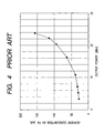
- Fig. 4 shows the relationship between the transmit signal level (output power) of a transmitter using the first gain adjusting means and the current consumption by the power amplifying stage 31.
- the required transmit signal level when the required transmit signal level is in a high range, the current consumption by the power amplifying stage 31 increases.
- the rate of variation of the current consumption dependent on the variation of the required transmit signal level is relatively mild, remaining between 30 and 40 mA, but if the required transmit signal level exceeds 10 dBm to approach or reach 24 dBm, the rate of variation of the current consumption dependent on the variation of the required transmit signal level increases to a range from 40 mA to 160 mA approximately.
- Fig. 5 is a block diagram of essential parts of a transmitter using a second gain adjusting means in a known mobile telephone.
- this transmitter is provided with a variable-gain power amplifying stage (PA) 41, a fixed-gain drive amplifying stage (DA) 42, a transmit signal generator 43, a gain control voltage generator 44, a transmit signal output terminal 45 and a transmit data (TX data) input terminal 46.
- PA variable-gain power amplifying stage
- DA fixed-gain drive amplifying stage
- TX data transmit data input terminal 46.
- the input terminal is connected to the transmit data input terminal 46 and the output terminal is connected to the input terminal of the variable-gain power amplifying stage 42.
- the output terminal of the fixed-gain drive amplifying stage 42 is connected to the input terminal of the variable gain power amplifying stage 41.
- the output terminal is connected to the transmit signal output terminal 45 and the control terminal is connected to the output terminal of the gain control voltage generator 44.
- the transmit signal generator 43 forms a carrier frequency, and modulates the formed carrier frequency with transmit data (TX data) supplied to the transmit data input terminal 46 to generate a transmit signal, and the generated transmit signal is supplied to the drive amplifying stage 42 that follows.
- the gain control voltage generator 44 generates a gain control voltage corresponding to the level of the receive signal that has been received (the field strength of the receive wave), and the gain control voltage so obtained is supplied to the variable-gain power amplifying stage 41.
- the transmit signal output terminal 45 is connected to a transmission antenna (now shown in Fig. 5).
- the transmitter using the second gain adjusting means having the above-described configuration operates in the following manner.
- the controller detects a receive signal level representing the field strength of the receive wave. If the detected receive signal level is relatively low, the gain control voltage generator 44 generates a gain control signal to increase the signal gain of the variable-gain power amplifying stage 41 according to the relative level of the receive signal level, and supplies it to the variable-gain power amplifying stage 41.
- the gain control voltage generator 44 If the detected receive signal level is relatively high, the gain control voltage generator 44 generates a gain control signal to reduce the signal gain of the variable-gain power amplifying stage 41 according to the relative level of the receive signal level, and supplies it to the variable-gain power amplifying stage 41.
- the variable-gain drive amplifying stage 42 amplifies the transmit signal supplied from the transmit signal generator 43, and supplies the amplified signal to the variable-gain power amplifying stage 41.
- the variable-gain power amplifying stage 41 amplifies in power the supplied transmit signal with a signal gain corresponding to the gain control signal, and supplies the amplified transmit signal to the transmission antenna via the transmit signal output terminal 45 to cause it to be transmitted from the transmission antenna.
- the transmit signal level required then is so controlled as to be raised when the receive signal level is low and, conversely, to be lowered when the receive signal level is high.
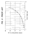
- Fig. 6 shows the relationship between the transmit signal level (output power) of a transmitter using the second gain adjusting means and the current consumption by the power amplifying stage 41.
- the required transmit signal level when the required transmit signal level is in a high range, the current consumption by the power amplifying stage 41 increases.
- the rate of variation of the current consumption dependent on the variation of the required transmit signal level is relatively mild, remaining between 10 and 35 mA, but if the required transmit signal level exceeds 12 dBm to approach or reach 24 dBm, the rate of variation of the current consumption dependent on the variation of the required transmit signal level increases to a range from 35 mA to 160 mA approximately.
- the transmitter using the second gain adjusting means consumes somewhat less current in its power amplifying stage, while in the transmit signal level range from 19 to 24 dBm, the transmitter using the first gain adjusting means consumes slightly less current in its power amplifying stage.
- a cordless mobile telephone uses a battery as its power source, when the mobile telephone is used beyond a certain length of time, its battery becomes exhausted and the mobile telephone can no longer be used. For this reason, it is required that the power source battery of a mobile telephone be extended in durability as long as practicable to ensure a long service life of the telephone, and this requirement applies alike to a mobile telephone having a transmitter using the first gain adjusting means and one having a transmitter using the second gain adjusting means, both described above.
- variable gain amplifying stages 32 and 41 are so adjusted as to achieve the required transmit signal level according to the relative level of the receive signal, the service life of the power source battery is extended by reducing the current consumption of the variable gain amplifying stage 32 or 41 when the required transmit signal level is adjusted to be relatively low, but the elongation of the battery's life is not sufficient, by no means satisfactory.
- An object of the present invention attempted against this technical background, is to provide a transmitter which adjusts its output power so as to reduce the current consumption of the power amplifying stage by selectively using a gain adjusting means according to the range of the required transmit signal level, in achieving the required transmit signal level correspondingly to the receive signal level.
- a transmitter adjusting output power is provided with a high-frequency signal generator for modulating a carrier frequency with transmit data to generate a transmit signal; a variable-gain drive amplifying stage for preamplifying the transmit signal; a variable-gain power amplifying stage for amplifying the preamplified transmit signal in power and supplying a transmit signal of a required signal level to an antenna; and a gain control voltage generator for generating a first gain control voltage with which to adjust the signal gain of the variable-gain drive amplifying stage and a second gain control voltage with which to adjust the signal gain of the variable-gain power amplifying stage, wherein the gain control voltage generator generates the second gain control voltage when the required signal level of the transmit signal is not above a certain fixed level to adjust the signal gain of the variable-gain power amplifying stage and, when the required signal level of the transmit signal is not below a certain fixed level, generates the first gain control voltage to adjust the signal gain of the variable-gain drive amplifying stage.
- This configuration enables, when the required transmit signal level is to be set within a range not higher than a certain fixed level, the current consumption of the power amplifying stage to be reduced at each required transmit signal level within that range by adjusting the signal gain of the variable-gain power amplifying stage and, when the required transmit signal level is to be set within a range not lower than a certain fixedlevel, the current consumption of the power amplifying stage to be reduced at each required transmit signal level within that range by adjusting the signal gain of the variable-gain power amplifying stage.
- a transmitter of this configuration can more effectively reduce the current consumption of the power amplifying stage for each required transmit signal level, making it possible to restrain the exhaustion of the power source battery and to extend the service life of a mobile telephone.
- the fixed level be the transmit signal level at the intersection of the characteristic curve representing the relationship between the transmit signal level achieved by adjusting the signal gain of the variable-gain drive amplifying stage and the current consumption of the power amplifying stage and that representing the relationship between the transmit signal level achieved by adjusting the signal gain of the variable-gain power amplifying stage and the current consumption of the power amplifying stage.
- This configuration allows selective use, according to the range of the required transmit signal level, of the characteristic curve representing the relationship between the transmit signal level achieved by adjusting the signal gain of the variable-gain drive amplifying stage and the current consumption of the power amplifying stage or that representing the relationship between the transmit signal level achieved by adjusting the signal gain of the variable-gain power amplifying stage and the current consumption of the power amplifying stage, making it possible to reduce the current consumption of the power amplifying stage for each required transmit signal level in a satisfactory way.
- Fig. 1 is a block diagram illustrating one embodiment of the configuration of a transmitter adjusting output power according to the present invention.
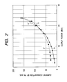
- Fig. 2 is a characteristic diagram illustrating the relationship between the transmit signal level (output power) and the current consumption of the power amplifying stage in the transmitter adjusting output power shown in Fig. 1.
- Fig. 3 is a block diagram illustrating the configuration of essential parts of a transmitter using the first gain adjusting means in a known mobile telephone.
- Fig. 4 is a characteristic diagram illustrating the relationship between the transmit signal level (output power) and the current consumption of the power amplifying stage in the transmitter using the first gain adjusting means shown in Fig. 3.
- Fig. 5 is a block diagram illustrating the configuration of essential parts of a transmitter using the second gain adjusting means in a known mobile telephone.
- Fig. 6 is a characteristic diagram illustrating the relationship between the transmit signal level (output power) and the current consumption of the power amplifying stage in the transmitter using the second gain adjusting means shown in Fig. 5.
- Fig. 1 which is a block diagram of the embodiment of the configuration of a transmitter adjusting output power according to the invention, shows the essential parts of a mobile telephone including this transmitter.
- the mobile telephone including the transmitter embodying the invention in this mode consists of a variable-gain power amplifying stage (PA) 1, a variable-gain drive amplifying stage (DA) 2, a buffer amplifying stage (BA) 3, a synthesizer (SYS, high-frequency signal generator) 4, a controller (CPU) 5, a power controller (PCC, gain control voltage generator) 5 1 , a first digital-to-analog converter (D/A) 6, a second digital-to-analog converter (D/A) 7, a ROM 8, a receiver circuit (REC) 9, a transmit/receive change-over switch 10, a transmit (TX) data input terminal 11, a receive (RX) data output terminal 12, and a transmission/reception antenna 13.
- PA variable-gain power amplifying stage
- DA variable-gain drive amplifying stage
- BA buffer amplifying stage
- SYS high-frequency signal generator
- PCC power controller
- REC receiver circuit
- REC transmit/receive change-over switch 10
- the power controller 5 1 is built into the controller 5.
- the circuit section including the variable-gain drive amplifying stage 2, the buffer amplifying stage 3, synthesizer 4, the controller 5, the power controller 51, the first digital-to-analog converter 6, the second digital-to-analog converter 7, the ROM 8 and the receiver circuit 9 is configured of a single integrated circuit (IC).
- the synthesizer 4 which forms a carrier frequency by frequency synthesis, sets the carrier frequency with a channel control signal (CH Cont) supplied from the controller 5.
- the carrier frequency so formed is modulated with transmit data (TX data) supplied to the transmit data input terminal 11, and a transmit signal consisting of the modulated carrier frequency are generated.
- the power controller 5 1 selectively generates a first gain control signal in the digital form or a second gain control signal in the digital form according to the level of the receive signal supplied to the controller 5.
- the ROM 8 stores a transmit signal level (a fixed level; how to set this fixed level will be described afterwards) indicating the point of time of switching between the supply of the first gain control signal and that of the second gain control signal from the power controller 5 1 .
- a first input terminal is connected to the controller 5, a second input terminal is connected to the transmit data input terminal 11, and the output terminal is connected to the input terminal of the buffer amplifying stage 3.
- the input terminal is connected to the output terminal of the buffer amplifying stage 3
- the output terminal is connected to the input terminal of the variable-gain power amplifying stage 1
- the control terminal is connected to the output terminal of the second digital-to-analog converter 7.
- the output terminal is connected to one of the fixed contacts of the transmit/receive change-over switch 10, and the control terminal is connected to the output terminal of the first digital-to-analog converter 6.
- the input terminal is connected to the controller 5, and of the second digital-to-analog converter 7 the input terminal is connected to the controller 5.
- the ROM 8 is also connected to the controller 5.
- the input terminal is connected to the other fixed contacts of the transmit/receive change-over switch 10, the output terminal is connected to the receive data output terminal 12, and the control terminal is connected to the controller 5.
- a movable contact is connected to the transmission/reception antenna 13.
- the mobile telephone including the transmitter embodying the invention in this mode configured as described above operates as stated below.
- the transmit/receive change-over switch 10 When the mobile telephone is in its reception mode and the contact of the transmit/receive change-over switch 10 is in the position indicated by the dotted line, if the transmission wave from the other party's mobile telephone (not shown in Fig. 1) is received by the transmission/reception antenna 13, a receive signal is supplied to the receiver circuit 9 from the transmission/reception antenna 13 via the transmit/receive change-over switch 10.
- the receiver circuit 9 amplifies and detects the supplied receive signal to obtain receive (RX) data, and generates an RSSI signal representing the receive signal level.
- the obtained receive data are supplied from the receiver circuit 9 to the receive data output terminal 12, and the RSSI signal is supplied from the receiver circuit 9 to the controller 5.
- the controller 5 detects the receive signal level from the receiver circuit 9 on the basis of the supplied RSSI signal, and sets the transmit signal level required for supplying an output from the variable-gain power amplifying stage 1 on the basis of the detected receive signal level.
- the controller 5 compares the transmit signal level that has been set with the fixed level read out of the ROM 8 and, if the comparison reveals that the set transmit signal level is lower than the fixed level, causes the power controller 51 to generate a first gain control signal in the digital form to supply it to the first digital-to-analog converter 6.
- the first digital-to-analog converter 6 converts the first gain control signal in the digital form into a first gain control voltage in the analog form, and supplies it to the variable-gain power amplifying stage 1.
- the synthesizer 4 generates a transmit signal by modulating the carrier frequency with transmit data supplied to the transmit data input terminal 11, and supplies this transmit signal to the buffer amplifying stage 3.
- the buffer amplifying stage 3 amplifies the transmit signal, and supplies the amplified transmit signal to the variable-gain drive amplifying stage 2.
- the variable-gain drive amplifying stage 2 since no second gain control voltage in the analog form is supplied at this point of time, amplifies the transmit signal with a fixed gain, and supplies the amplified transmit signal to the variable-gain power amplifying stage 1.
- variable-gain power amplifying stage 1 amplifies in power the transmit signal with a signal gain matching the supplied first gain control voltage, and supplies the amplified transmit signal to the transmission/ reception antenna 13 via the transmit/receive change-over switch 10, and transmits it from the transmission/reception antenna 13.
- the controller 5 compares the transmit signal level that has been set with a fixed level read out of the ROM 8 and, if the comparison reveals that the set transmit signal level is higher than the fixed level, causes the power controller 5 1 to generate a second gain control signal in the digital form to supply it to the second digital-to-analog converter 7.
- the second digital-to-analog converter 7 converts the second gain control signal in the digital form into a second gain control voltage in the analog form, and supplies it to the variable-gain drive amplifying stage 2.
- the synthesizer 4 generates a transmit signal by modulating the carrier frequency with transmit data supplied to the transmit data input terminal 11, and supplies this transmit signal to the buffer amplifying stage 3.
- the buffer amplifying stage 3 amplifies the transmit signal, and supplies the amplified transmit signal to the variable-gain drive amplifying stage 2.
- the variable-gain drive amplifying stage 2 amplifies the transmit signal with a signal gain matching the supplied second gain control voltage, and supplies the amplified transmit signal to the variable-gain power amplifying stage 1.
- the variable-gain power amplifying stage 1 since no first gain control voltage in the analog form is supplied at this point of time, amplifies in power the transmit signal with a fixed gain, supplies the amplified transmit signal to the transmission/reception antenna 13 via the transmit/ receive change-over switch 10, and transmits it from the transmission/reception antenna 13.
- Fig. 2 here is a characteristic diagram illustrating the relationship between the required transmit signal level (output power) and the current consumption of the power amplifying stage 1 in the transmitter in this mode of embodying the invention shown in Fig. 1.
- the characteristic curve represented by the solid line a and by the dotted line a' are the same as the characteristic curve in the characteristic diagram of Fig. 6, and the characteristic curve represented here by the solid line b and the dotted line b' are the same as the characteristic curve in the characteristic diagram of Fig. 4.
- the current consumption of the variable-gain power amplifying stage 1 varies with any variation in the required transmit signal level.
- the transmitter embodying the invention in this mode when the required transmit signal level is in a range from 2 to 19 dBm, supplies the first gain control voltage to the variable-gain power amplifying stage 1 and obtains the required transmit signal level by controlling the signal gain, the current consumption of the variable gain power amplifying stage 1 represented by the solid line a of Fig. 2 is generally less than that represented by the dotted line b' of Fig. 2.
- the current consumption of the variable-gain power amplifying stage 1 represented by the solid line b of Fig. 2 is generally less that represented by the dotted line a' of Fig. 2.
- the mobile telephone having a transmitter using the above-described known first gain adjusting means is in a range from 30 to 160 mA in the current consumption of the power amplifying stage 31 as illustrated by the characteristic diagram of Fig. 4 when the required transmit signal level corresponding to the receive signal level is in a range from 3 to 24 dBm.
- the mobile telephone having a transmitter using the above-described known second gain adjusting means is in a range from 10 to 160 mA in the current consumption of the variable gain power amplifying stage 41 as illustrated by the characteristic diagram of Fig. 6 when the required transmit signal level corresponding to the receive signal level is in a range from 2 to 24 dBm.
- the transmitter using the second gain adjusting means is generally less in the current consumption of the variable-gain power amplifying stage 41, while in a range of the required transmit signal level from 19 to 24 dBm, the transmitter using the first gain adjusting means is generally less in the current consumption of the power amplifying stage 31.
- the invention is the idea that, by effectively combining the first gain adjusting means and the second gain adjusting means and selectively using the first gain adjusting means or the second gain adjusting means according to the range of the required transmit signal level, in other words by selective use of means to control the signal gain of the variable-gain drive amplifying stage 2 with the second gain control signal or of means to control the signal gain of the variable-gain power amplifying stage 1 with the first gain control signal, the current consumption of the variable-gain power amplifying stage 1 can be kept less than that of the transmitter using the means to control the signal gain of the variable-gain drive amplifying stage 2 with the second gain control signal or the means to control the signal gain of the variable-gain power amplifying stage 1 with the first gain control signal.
- the transmit signal level at the intersection of the characteristic curve represented by the solid line a and the dotted line a' and that represented by the solid line b and the dotted line b', 19 dBm in this case is stored into the ROM 8 as the fixed level, and if the required transmit signal level has to be set not higher than the fixed level (19 dBm), a current consumption characteristic of the variable-gain power amplifying stage 1 along the characteristic curve represented by the solid line a is obtained by controlling the signal gain of the variable-gain power amplifying stage 1, or if the required transmit signal level has to be set not lower than the fixed level (19 dBm), a current consumption characteristic of the variable-gain power amplifying stage 1 along the characteristic curve represented by the solid line b is obtained by controlling the signal gain of the variable-gain drive amplifying stage 2.
- gain control means whose variable-gain power amplifying stage 1 consumes less current is selectively used according to the range of the required transmit signal level, the consumption of power by a mobile telephone when it is in use can be reduced, and the duration of communication possible with the battery power source of the telephone can be extended correspondingly.
- the fixed level according to the invention is not limited to the intersection of the two characteristic curves, but may be a vicinity of the transmit signal level, for instance, in a range from 2 to 3 dBm below and above that transmit signal level.
- the transmitter adjusting output power according to the invention is not limited to use in a mobile telephone, but it can as well be used for adjusting the output power of the handset of a mobile telephone.
Abstract
Description
- The present invention relates to a transmitter adjusting output power, and more particularly to a transmitter which, driven by a battery as in the handset of a mobile telephone, adjusts output power so as to minimize the exhaustion of the power source battery when adjusting the output power of transmit signals.
- Usually, a cordless mobile telephone, when communicating with another mobile telephone, is subject to fluctuations in the field intensity of the receive wave reaching each mobile telephone depending on the distance between the calling party's mobile telephone and the corresponding telephone relaying base and the state of wave transmission in-between as well as the distance between the other party's mobile telephone and the corresponding telephone relaying base and the state of wave transmission in-between.
- Incidentally, if the field intensity of the receive wave reaching the calling party's mobile telephone is weak, the link with the other party may be so much affected by noise and the like that satisfactory communication is made difficult or sometimes even impossible. On the other hand, if the field intensity of the receive wave reaching the calling party's mobile telephone is strong, the transmission/reception of the wave may be taking place at a signal level which is higher than a necessary signal level, and this is not necessarily desirable because the exhaustion of the power source battery of the mobile telephone would increase correspondingly.
- For this reason, in order to ensure satisfactory communication between one mobile telephone and the other mobile telephone and to avoid an unnecessary increase in battery exhaustion, when a wave transmitted from the other mobile telephone is received, the field strength of the receive wave should be detected and, if the detected field strength is relatively large, the signal gain of the transmitter should be adjusted according to the relative level of the detected field strength to reduce the level of the transmit signal from the transmitter. If the detected field strength is relatively weak, the signal gain of the transmitter should be adjusted according to the relative level of the detected field strength to enhance the level of the transmit signal from the transmitter. Thus, by adjusting the level of the transmit signal sent from the respective transmitters of two mutually communicating mobile telephones, the field strength of the wave received by each other's mobile telephone can be regulated to a standard level, thereby enabling the two mobile telephones to communicate satisfactorily and prevent both mobile telephones from suffering unnecessary exhaustion of their respective power source batteries.
- Adjusting means known to be available according to the prior art for signal gains of transmitters in mobile telephone include first gain adjusting means which fixes the signal gain in the power amplifying stage and makes controllable the signal gain in the drive amplifying stage with a gain control voltage to adjust the level of the transmit signal as required, and second gain adjusting means which fixes the signal gain in the drive amplifying stage and makes controllable the signal gain in the power amplifying stage with a gain control voltage to adjust the level of the transmit signal as required.
- Fig. 3 is a block diagram illustrating the configuration of essential parts of a transmitter using a first gain adjusting means in a known mobile telephone.
- As shown in Fig. 3, this transmitter is provided with a fixed-gain power amplifying stage (PA) 31, a variable-gain drive amplifying stage (DA) 32, a
transmit signal generator 33, a gaincontrol voltage generator 34, a transmitsignal output terminal 35 and a transmit data (TX data)input terminal 36. Of thetransmit signal generator 33, the input terminal is connected to the transmitdata input terminal 36 and the output terminal is connected to the input terminal of the variable-gaindrive amplifying stage 32. Of the variable-gain power amplifyingstage 32, the control terminal is connected to the output terminal of the gaincontrol voltage generator 34 and the output terminal is connected to the input terminal of the fixed-gain power amplifyingstage 31. Of the fixed-gain power amplifyingstage 31, the output terminal is connected to the transmitsignal output terminal 35. - In this case, the
transmit signal generator 33 forms a carrier frequency, and modulates the formed carrier frequency with transmit data (TX data) supplied to the transmitdata input terminal 36 to generate a transmit signal, and the generated transmit signal is supplied to the variable-gaindrive amplifying stage 32 that follows. The gaincontrol voltage generator 34 generates a gain control voltage corresponding to the level of the receive signal that has been received (the field strength of the receive wave), and the gain control voltage so obtained is supplied to the variable-gaindrive amplifying stage 32. Further, the transmitsignal output terminal 35 is connected to a transmission antenna (not shown in Fig. 3). - Schematically, the transmitter using the first gain adjusting means having the above-described configuration operates in the following manner.
- As the receiver (not shown in Fig. 3) of a mobile telephone receives a signal transmitted by the mobile telephone of the other party to the call, the controller (not shown in Fig. 3 either) detects a receive signal level representing the field strength of the receive wave. If the detected receive signal level is relatively low, the gain
control voltage generator 34 generates a gain control signal to increase the signal gain of the variable-gaindrive amplifying stage 32 according to the relative level of the receive signal level, and supplies it to the variable-gaindrive amplifying stage 32. If the detected receive signal level is relatively high, the gaincontrol voltage generator 34 generates a gain control signal to reduce the signal gain of the variable-gaindrive amplifying stage 32 according to the relative level of the receive signal level, and supplies it to the variable-gaindrive amplifying stage 32. After that, the variable-gaindrive amplifying stage 32 amplifies the transmit signal supplied from thetransmit signal generator 33 with a signal gain corresponding to the gain control signal, and supplies the amplified signal to the power amplifyingstage 31. The power amplifyingstage 31 further amplifies in power the supplied transmit signal, and supplies the amplified transmit signal to the transmission antenna via the transmitsignal output terminal 35 to cause it to be transmitted from the transmission antenna. The transmit signal level required then is so controlled as to be raised when the receive signal level is low and, conversely, to be lowered when the receive signal level is high. - Hereupon, Fig. 4 shows the relationship between the transmit signal level (output power) of a transmitter using the first gain adjusting means and the current consumption by the power amplifying
stage 31. - As illustrated in Fig. 4, in the transmitter using the first gain adjusting means, when the required transmit signal level is in a high range, the current consumption by the power amplifying
stage 31 increases. In this case, if the required transmit signal level is within the range from 3 to 10 dBm, the rate of variation of the current consumption dependent on the variation of the required transmit signal level is relatively mild, remaining between 30 and 40 mA, but if the required transmit signal level exceeds 10 dBm to approach or reach 24 dBm, the rate of variation of the current consumption dependent on the variation of the required transmit signal level increases to a range from 40 mA to 160 mA approximately. - Next, Fig. 5 is a block diagram of essential parts of a transmitter using a second gain adjusting means in a known mobile telephone.
- As illustrated in Fig. 5, this transmitter is provided with a variable-gain power amplifying stage (PA) 41, a fixed-gain drive amplifying stage (DA) 42, a
transmit signal generator 43, a gaincontrol voltage generator 44, a transmitsignal output terminal 45 and a transmit data (TX data)input terminal 46. - Of the
transmit signal generator 43, the input terminal is connected to the transmitdata input terminal 46 and the output terminal is connected to the input terminal of the variable-gain power amplifyingstage 42. The output terminal of the fixed-gaindrive amplifying stage 42 is connected to the input terminal of the variable gain power amplifyingstage 41. Of the variable gain power amplifyingstage 41 the output terminal is connected to the transmitsignal output terminal 45 and the control terminal is connected to the output terminal of the gaincontrol voltage generator 44. - Also in this case, the
transmit signal generator 43 forms a carrier frequency, and modulates the formed carrier frequency with transmit data (TX data) supplied to the transmitdata input terminal 46 to generate a transmit signal, and the generated transmit signal is supplied to thedrive amplifying stage 42 that follows. The gaincontrol voltage generator 44 generates a gain control voltage corresponding to the level of the receive signal that has been received (the field strength of the receive wave), and the gain control voltage so obtained is supplied to the variable-gain power amplifyingstage 41. Further, the transmitsignal output terminal 45 is connected to a transmission antenna (now shown in Fig. 5). - Schematically, the transmitter using the second gain adjusting means having the above-described configuration operates in the following manner.
- As the receiver (not shown in Fig. 5) of a mobile telephone receives a signal transmitted by the mobile telephone of the other party to the call, the controller (not shown in Fig. 5 either) detects a receive signal level representing the field strength of the receive wave. If the detected receive signal level is relatively low, the gain
control voltage generator 44 generates a gain control signal to increase the signal gain of the variable-gain power amplifyingstage 41 according to the relative level of the receive signal level, and supplies it to the variable-gain power amplifyingstage 41. If the detected receive signal level is relatively high, the gaincontrol voltage generator 44 generates a gain control signal to reduce the signal gain of the variable-gain power amplifyingstage 41 according to the relative level of the receive signal level, and supplies it to the variable-gain power amplifyingstage 41. After that, the variable-gaindrive amplifying stage 42 amplifies the transmit signal supplied from thetransmit signal generator 43, and supplies the amplified signal to the variable-gain power amplifyingstage 41. The variable-gain power amplifyingstage 41 amplifies in power the supplied transmit signal with a signal gain corresponding to the gain control signal, and supplies the amplified transmit signal to the transmission antenna via the transmitsignal output terminal 45 to cause it to be transmitted from the transmission antenna. The transmit signal level required then is so controlled as to be raised when the receive signal level is low and, conversely, to be lowered when the receive signal level is high. - Here, Fig. 6 shows the relationship between the transmit signal level (output power) of a transmitter using the second gain adjusting means and the current consumption by the power amplifying
stage 41. - As illustrated in Fig. 6, also in the transmitter using the second gain adjusting means, like the transmitter using the first gain adjusting means, when the required transmit signal level is in a high range, the current consumption by the power amplifying
stage 41 increases. In this case, if the required transmit signal level is within the range from 2 to 12 dBm, the rate of variation of the current consumption dependent on the variation of the required transmit signal level is relatively mild, remaining between 10 and 35 mA, but if the required transmit signal level exceeds 12 dBm to approach or reach 24 dBm, the rate of variation of the current consumption dependent on the variation of the required transmit signal level increases to a range from 35 mA to 160 mA approximately. - To add, to compare the characteristic diagram of Fig. 4 with that of Fig. 6, if the required transmit signal level is within the range from 2 to 19 dBm, the transmitter using the second gain adjusting means consumes somewhat less current in its power amplifying stage, while in the transmit signal level range from 19 to 24 dBm, the transmitter using the first gain adjusting means consumes slightly less current in its power amplifying stage.
- Since a cordless mobile telephone uses a battery as its power source, when the mobile telephone is used beyond a certain length of time, its battery becomes exhausted and the mobile telephone can no longer be used. For this reason, it is required that the power source battery of a mobile telephone be extended in durability as long as practicable to ensure a long service life of the telephone, and this requirement applies alike to a mobile telephone having a transmitter using the first gain adjusting means and one having a transmitter using the second gain adjusting means, both described above.
- In a mobile telephone having a transmitter using the first gain adjusting means or one having a transmitter using second gain adjusting means, their respective variable
gain amplifying stages gain amplifying stage - An object of the present invention, attempted against this technical background, is to provide a transmitter which adjusts its output power so as to reduce the current consumption of the power amplifying stage by selectively using a gain adjusting means according to the range of the required transmit signal level, in achieving the required transmit signal level correspondingly to the receive signal level.
- In order to achieve the above-stated object, a transmitter adjusting output power according to the invention is provided with a high-frequency signal generator for modulating a carrier frequency with transmit data to generate a transmit signal; a variable-gain drive amplifying stage for preamplifying the transmit signal; a variable-gain power amplifying stage for amplifying the preamplified transmit signal in power and supplying a transmit signal of a required signal level to an antenna; and a gain control voltage generator for generating a first gain control voltage with which to adjust the signal gain of the variable-gain drive amplifying stage and a second gain control voltage with which to adjust the signal gain of the variable-gain power amplifying stage, wherein the gain control voltage generator generates the second gain control voltage when the required signal level of the transmit signal is not above a certain fixed level to adjust the signal gain of the variable-gain power amplifying stage and, when the required signal level of the transmit signal is not below a certain fixed level, generates the first gain control voltage to adjust the signal gain of the variable-gain drive amplifying stage.
- This configuration enables, when the required transmit signal level is to be set within a range not higher than a certain fixed level, the current consumption of the power amplifying stage to be reduced at each required transmit signal level within that range by adjusting the signal gain of the variable-gain power amplifying stage and, when the required transmit signal level is to be set within a range not lower than a certain fixedlevel, the current consumption of the power amplifying stage to be reduced at each required transmit signal level within that range by adjusting the signal gain of the variable-gain power amplifying stage. Therefore, compared with a transmitter which adjusts the signal gain of the variable-gain drive amplifying stage and a transmitter which adjusts the signal gain of the variable-gain power amplifying stage to achieve a required transmit signal level, a transmitter of this configuration can more effectively reduce the current consumption of the power amplifying stage for each required transmit signal level, making it possible to restrain the exhaustion of the power source battery and to extend the service life of a mobile telephone.
- Moreover, by this configuration, when the required transmit signal level is to be set in a higher range, the signal gain of the variable-gain drive amplifying stage is adjusted and the signal gain of the variable-gain power amplifying stage is not adjusted. Accordingly, the occurrence of signal distortion in the variable-gain power amplifying stage due to a signal gain when the required transmit signal level is high can be restrained.
- Further according to the invention, it is preferable that the fixed level be the transmit signal level at the intersection of the characteristic curve representing the relationship between the transmit signal level achieved by adjusting the signal gain of the variable-gain drive amplifying stage and the current consumption of the power amplifying stage and that representing the relationship between the transmit signal level achieved by adjusting the signal gain of the variable-gain power amplifying stage and the current consumption of the power amplifying stage.
- This configuration allows selective use, according to the range of the required transmit signal level, of the characteristic curve representing the relationship between the transmit signal level achieved by adjusting the signal gain of the variable-gain drive amplifying stage and the current consumption of the power amplifying stage or that representing the relationship between the transmit signal level achieved by adjusting the signal gain of the variable-gain power amplifying stage and the current consumption of the power amplifying stage, making it possible to reduce the current consumption of the power amplifying stage for each required transmit signal level in a satisfactory way.
- Fig. 1 is a block diagram illustrating one embodiment of the configuration of a transmitter adjusting output power according to the present invention.
- Fig. 2 is a characteristic diagram illustrating the relationship between the transmit signal level (output power) and the current consumption of the power amplifying stage in the transmitter adjusting output power shown in Fig. 1.
- Fig. 3 is a block diagram illustrating the configuration of essential parts of a transmitter using the first gain adjusting means in a known mobile telephone.
- Fig. 4 is a characteristic diagram illustrating the relationship between the transmit signal level (output power) and the current consumption of the power amplifying stage in the transmitter using the first gain adjusting means shown in Fig. 3.
- Fig. 5 is a block diagram illustrating the configuration of essential parts of a transmitter using the second gain adjusting means in a known mobile telephone.
- Fig. 6 is a characteristic diagram illustrating the relationship between the transmit signal level (output power) and the current consumption of the power amplifying stage in the transmitter using the second gain adjusting means shown in Fig. 5.
- A preferred embodiment of the present invention will be described below with reference to accompanying drawings.
- Fig. 1, which is a block diagram of the embodiment of the configuration of a transmitter adjusting output power according to the invention, shows the essential parts of a mobile telephone including this transmitter.
- As shown in Fig. 1, the mobile telephone including the transmitter embodying the invention in this mode consists of a variable-gain power amplifying stage (PA) 1, a variable-gain drive amplifying stage (DA) 2, a buffer amplifying stage (BA) 3, a synthesizer (SYS, high-frequency signal generator) 4, a controller (CPU) 5, a power controller (PCC, gain control voltage generator) 51, a first digital-to-analog converter (D/A) 6, a second digital-to-analog converter (D/A) 7, a
ROM 8, a receiver circuit (REC) 9, a transmit/receive change-over switch 10, a transmit (TX)data input terminal 11, a receive (RX)data output terminal 12, and a transmission/reception antenna 13. Thepower controller 51 is built into thecontroller 5. The circuit section including the variable-gain drive amplifying stage 2, thebuffer amplifying stage 3, synthesizer 4, thecontroller 5, thepower controller 51, the first digital-to-analog converter 6, the second digital-to-analog converter 7, theROM 8 and thereceiver circuit 9 is configured of a single integrated circuit (IC). - In this case, the synthesizer 4, which forms a carrier frequency by frequency synthesis, sets the carrier frequency with a channel control signal (CH Cont) supplied from the
controller 5. The carrier frequency so formed is modulated with transmit data (TX data) supplied to the transmitdata input terminal 11, and a transmit signal consisting of the modulated carrier frequency are generated. Thepower controller 51 selectively generates a first gain control signal in the digital form or a second gain control signal in the digital form according to the level of the receive signal supplied to thecontroller 5. TheROM 8 stores a transmit signal level (a fixed level; how to set this fixed level will be described afterwards) indicating the point of time of switching between the supply of the first gain control signal and that of the second gain control signal from thepower controller 51. - Of the synthesizer 4, a first input terminal is connected to the
controller 5, a second input terminal is connected to the transmitdata input terminal 11, and the output terminal is connected to the input terminal of thebuffer amplifying stage 3. Of the variable-gain drive amplifying stage 2, the input terminal is connected to the output terminal of thebuffer amplifying stage 3, the output terminal is connected to the input terminal of the variable-gain power amplifying stage 1, and the control terminal is connected to the output terminal of the second digital-to-analog converter 7. Of the variable-gain power amplifying stage 1, the output terminal is connected to one of the fixed contacts of the transmit/receive change-over switch 10, and the control terminal is connected to the output terminal of the first digital-to-analog converter 6. Of the first digital-to-analog converter 6, the input terminal is connected to thecontroller 5, and of the second digital-to-analog converter 7 the input terminal is connected to thecontroller 5. TheROM 8 is also connected to thecontroller 5. Of thereceiver circuit 9, the input terminal is connected to the other fixed contacts of the transmit/receive change-over switch 10, the output terminal is connected to the receivedata output terminal 12, and the control terminal is connected to thecontroller 5. Of the transmit/receive change-over switch 10, a movable contact is connected to the transmission/reception antenna 13. - The mobile telephone including the transmitter embodying the invention in this mode configured as described above operates as stated below.
- When the mobile telephone is in its reception mode and the contact of the transmit/receive change-
over switch 10 is in the position indicated by the dotted line, if the transmission wave from the other party's mobile telephone (not shown in Fig. 1) is received by the transmission/reception antenna 13, a receive signal is supplied to thereceiver circuit 9 from the transmission/reception antenna 13 via the transmit/receive change-over switch 10. Thereceiver circuit 9 amplifies and detects the supplied receive signal to obtain receive (RX) data, and generates an RSSI signal representing the receive signal level. The obtained receive data are supplied from thereceiver circuit 9 to the receivedata output terminal 12, and the RSSI signal is supplied from thereceiver circuit 9 to thecontroller 5. - Then, when the mobile telephone is set into its transmission mode, the contact of the transmit/receive change-
over switch 10 is turned over to the position indicated by the solid line. Then thecontroller 5 detects the receive signal level from thereceiver circuit 9 on the basis of the supplied RSSI signal, and sets the transmit signal level required for supplying an output from the variable-gain power amplifying stage 1 on the basis of the detected receive signal level. Next, thecontroller 5 compares the transmit signal level that has been set with the fixed level read out of theROM 8 and, if the comparison reveals that the set transmit signal level is lower than the fixed level, causes thepower controller 51 to generate a first gain control signal in the digital form to supply it to the first digital-to-analog converter 6. The first digital-to-analog converter 6 converts the first gain control signal in the digital form into a first gain control voltage in the analog form, and supplies it to the variable-gain power amplifying stage 1. At the same time, the synthesizer 4 generates a transmit signal by modulating the carrier frequency with transmit data supplied to the transmitdata input terminal 11, and supplies this transmit signal to thebuffer amplifying stage 3. Thebuffer amplifying stage 3 amplifies the transmit signal, and supplies the amplified transmit signal to the variable-gain drive amplifying stage 2. The variable-gain drive amplifying stage 2, since no second gain control voltage in the analog form is supplied at this point of time, amplifies the transmit signal with a fixed gain, and supplies the amplified transmit signal to the variable-gain power amplifying stage 1. The variable-gain power amplifying stage 1 amplifies in power the transmit signal with a signal gain matching the supplied first gain control voltage, and supplies the amplified transmit signal to the transmission/reception antenna 13 via the transmit/receive change-over switch 10, and transmits it from the transmission/reception antenna 13. - On the other hand, the
controller 5 compares the transmit signal level that has been set with a fixed level read out of theROM 8 and, if the comparison reveals that the set transmit signal level is higher than the fixed level, causes thepower controller 51 to generate a second gain control signal in the digital form to supply it to the second digital-to-analog converter 7. The second digital-to-analog converter 7 converts the second gain control signal in the digital form into a second gain control voltage in the analog form, and supplies it to the variable-gain drive amplifying stage 2. In this procedure again, the synthesizer 4 generates a transmit signal by modulating the carrier frequency with transmit data supplied to the transmitdata input terminal 11, and supplies this transmit signal to thebuffer amplifying stage 3. Thebuffer amplifying stage 3 amplifies the transmit signal, and supplies the amplified transmit signal to the variable-gain drive amplifying stage 2. The variable-gain drive amplifying stage 2 amplifies the transmit signal with a signal gain matching the supplied second gain control voltage, and supplies the amplified transmit signal to the variable-gain power amplifying stage 1. The variable-gain power amplifying stage 1, since no first gain control voltage in the analog form is supplied at this point of time, amplifies in power the transmit signal with a fixed gain, supplies the amplified transmit signal to the transmission/reception antenna 13 via the transmit/ receive change-over switch 10, and transmits it from the transmission/reception antenna 13. - Fig. 2 here is a characteristic diagram illustrating the relationship between the required transmit signal level (output power) and the current consumption of the power amplifying stage 1 in the transmitter in this mode of embodying the invention shown in Fig. 1.
- Incidentally, in the characteristic diagram of Fig. 2, the characteristic curve represented by the solid line a and by the dotted line a' are the same as the characteristic curve in the characteristic diagram of Fig. 6, and the characteristic curve represented here by the solid line b and the dotted line b' are the same as the characteristic curve in the characteristic diagram of Fig. 4.
- As shown in Fig. 2, also in the transmitter embodying the invention in this mode, as in the transmitter using the above-described known first gain adjusting means and that using above-described known second gain adjusting means, the current consumption of the variable-gain power amplifying stage 1 varies with any variation in the required transmit signal level. In this case, since the transmitter embodying the invention in this mode, when the required transmit signal level is in a range from 2 to 19 dBm, supplies the first gain control voltage to the variable-gain power amplifying stage 1 and obtains the required transmit signal level by controlling the signal gain, the current consumption of the variable gain power amplifying stage 1 represented by the solid line a of Fig. 2 is generally less than that represented by the dotted line b' of Fig. 2. Further, since it supplies the second gain control voltage to the variable-gain drive amplifying stage 2 and obtains the required transmit signal level at the output of the variable-gain power amplifying stage 1 by controlling the signal gain when the required transmit signal level is in a range from 19 to 24 dBm, the current consumption of the variable-gain power amplifying stage 1 represented by the solid line b of Fig. 2 is generally less that represented by the dotted line a' of Fig. 2.
- To explain this point in further detail, the mobile telephone having a transmitter using the above-described known first gain adjusting means is in a range from 30 to 160 mA in the current consumption of the
power amplifying stage 31 as illustrated by the characteristic diagram of Fig. 4 when the required transmit signal level corresponding to the receive signal level is in a range from 3 to 24 dBm. The mobile telephone having a transmitter using the above-described known second gain adjusting means is in a range from 10 to 160 mA in the current consumption of the variable gainpower amplifying stage 41 as illustrated by the characteristic diagram of Fig. 6 when the required transmit signal level corresponding to the receive signal level is in a range from 2 to 24 dBm. And when the required transmit signal level is in a range from 3 to 19 dBm, the transmitter using the second gain adjusting means is generally less in the current consumption of the variable-gainpower amplifying stage 41, while in a range of the required transmit signal level from 19 to 24 dBm, the transmitter using the first gain adjusting means is generally less in the current consumption of thepower amplifying stage 31. Underlying the invention is the idea that, by effectively combining the first gain adjusting means and the second gain adjusting means and selectively using the first gain adjusting means or the second gain adjusting means according to the range of the required transmit signal level, in other words by selective use of means to control the signal gain of the variable-gain drive amplifying stage 2 with the second gain control signal or of means to control the signal gain of the variable-gain power amplifying stage 1 with the first gain control signal, the current consumption of the variable-gain power amplifying stage 1 can be kept less than that of the transmitter using the means to control the signal gain of the variable-gain drive amplifying stage 2 with the second gain control signal or the means to control the signal gain of the variable-gain power amplifying stage 1 with the first gain control signal. - For this reason, in this embodiment of the invention, the transmit signal level at the intersection of the characteristic curve represented by the solid line a and the dotted line a' and that represented by the solid line b and the dotted line b', 19 dBm in this case, is stored into the
ROM 8 as the fixed level, and if the required transmit signal level has to be set not higher than the fixed level (19 dBm), a current consumption characteristic of the variable-gain power amplifying stage 1 along the characteristic curve represented by the solid line a is obtained by controlling the signal gain of the variable-gain power amplifying stage 1, or if the required transmit signal level has to be set not lower than the fixed level (19 dBm), a current consumption characteristic of the variable-gain power amplifying stage 1 along the characteristic curve represented by the solid line b is obtained by controlling the signal gain of the variable-gain drive amplifying stage 2. - Since the transmitter adjusting output power embodying the invention in this mode, when a required transmit signal level is to be achieved, gain control means whose variable-gain power amplifying stage 1 consumes less current is selectively used according to the range of the required transmit signal level, the consumption of power by a mobile telephone when it is in use can be reduced, and the duration of communication possible with the battery power source of the telephone can be extended correspondingly.
- To add, although the foregoing embodiment uses as the fixed level to be stored in the
ROM 8 the transmit signal level at the intersection of the characteristic curve representing the relationship between the transmit signal level achieved by adjusting the signal gain of the variable-gain drive amplifying stage 2 and the current consumption of the power amplifying stage 1 and that representing the relationship between the transmit signal level achieved by adjusting the signal gain of the variable-gain power amplifying stage 1 and the current consumption of the power amplifying stage 1, the fixed level according to the invention is not limited to the intersection of the two characteristic curves, but may be a vicinity of the transmit signal level, for instance, in a range from 2 to 3 dBm below and above that transmit signal level. - Further, although the foregoing embodiment is an example in which the transmitter adjusting output power is used in a mobile telephone, the transmitter adjusting output power according to the invention is not limited to use in a mobile telephone, but it can as well be used for adjusting the output power of the handset of a mobile telephone.
Claims (2)
- A transmitter adjusting output power comprising: a high-frequency signal generator for modulating a carrier frequency with transmit data to generate a transmit signal; a variable-gain drive amplifying stage for preamplifying the transmit signal; a variable-gain power amplifying stage for amplifying the preamplified transmit signal in power and supplying a transmit signal of a required signal level to an antenna; and a gain control voltage generator for generating a first gain control voltage with which to adjust the signal gain of the variable-gain drive amplifying stage and a second gain control voltage with which to adjust the signal gain of the variable-gain power amplifying stage, wherein the gain control voltage generator generates the second gain control voltage when the required signal level of the transmit signal is not above a certain fixed level to adjust the signal gain of the variable-gain power amplifying stage and, when the required signal level of the transmit signal is not below a certain fixed level, generates the first gain control voltage to adjust the signal gain of the variable-gain drive amplifying stage.
- A transmitter adjusting output power according to Claim 1, wherein the fixed level is the transmit signal level at the intersection of the characteristic curve representing the relationship between the transmit signal level achieved by adjusting the signal gain of the variable-gain drive amplifying stage and the current consumption of the power amplifying stage and the characteristic curve representing the relationship between the transmit signal level achieved by adjusting the signal gain of the variable-gain power amplifying stage and the current consumption of the power amplifying stage.
Applications Claiming Priority (2)
| Application Number | Priority Date | Filing Date | Title |
|---|---|---|---|
| JP33298699 | 1999-11-24 | ||
| JP33298699A JP3739614B2 (en) | 1999-11-24 | 1999-11-24 | Transmitter for output power adjustment |
Publications (3)
| Publication Number | Publication Date |
|---|---|
| EP1104119A2 true EP1104119A2 (en) | 2001-05-30 |
| EP1104119A3 EP1104119A3 (en) | 2004-07-07 |
| EP1104119B1 EP1104119B1 (en) | 2006-02-22 |
Family
ID=18261037
Family Applications (1)
| Application Number | Title | Priority Date | Filing Date |
|---|---|---|---|
| EP00309464A Expired - Lifetime EP1104119B1 (en) | 1999-11-24 | 2000-10-27 | Transmitter adjusting output power |
Country Status (6)
| Country | Link |
|---|---|
| US (1) | US6304139B1 (en) |
| EP (1) | EP1104119B1 (en) |
| JP (1) | JP3739614B2 (en) |
| KR (1) | KR100375402B1 (en) |
| DE (1) | DE60026119T2 (en) |
| TW (1) | TW479424B (en) |
Cited By (1)
| Publication number | Priority date | Publication date | Assignee | Title |
|---|---|---|---|---|
| CN108601078A (en) * | 2018-03-19 | 2018-09-28 | 四川斐讯信息技术有限公司 | A kind of adjusting method of router and router transmission power |
Families Citing this family (16)
| Publication number | Priority date | Publication date | Assignee | Title |
|---|---|---|---|---|
| GB2351404B (en) * | 1999-06-24 | 2003-11-12 | Nokia Mobile Phones Ltd | A transmitter and a modulator therefor |
| US6721368B1 (en) * | 2000-03-04 | 2004-04-13 | Qualcomm Incorporated | Transmitter architectures for communications systems |
| JP3479835B2 (en) * | 2000-09-13 | 2003-12-15 | 日本電気株式会社 | Baseband gain control method and baseband gain control circuit |
| GB2393595B (en) * | 2002-09-26 | 2007-04-04 | Qualcomm | A transmitter and a method of calibrating power in signals output from a transmitter |
| US7310381B2 (en) * | 2003-06-16 | 2007-12-18 | Intel Corporation | Power amplifier pre-distortion device and method for orthogonal frequency division multiplexing |
| US7778596B2 (en) * | 2004-07-29 | 2010-08-17 | Qualcomm Incorporated | Airlink sensing watermarking repeater |
| JP4682750B2 (en) * | 2005-08-22 | 2011-05-11 | ソニー株式会社 | DA converter |
| US7711070B2 (en) * | 2005-08-25 | 2010-05-04 | Qualcomm, Incorporated | Method and apparatus for control of transmitter power consumption |
| KR20070082992A (en) * | 2006-02-20 | 2007-08-23 | 엘지이노텍 주식회사 | Set top box for two-way communication |
| DE102006035663B4 (en) * | 2006-07-31 | 2013-08-08 | Intel Mobile Communications GmbH | circuitry |
| KR100819294B1 (en) * | 2006-12-04 | 2008-04-02 | 삼성전자주식회사 | Device and method for controlling power of radio frequency in wireless terminal |
| US7684767B2 (en) * | 2007-02-26 | 2010-03-23 | Broadcom Corporation | Voice, data and RF integrated circuit with multiple modulation modes and methods for use therewith |
| FR2926944B1 (en) * | 2008-01-30 | 2010-03-26 | Wavecom | METHOD AND DEVICE FOR OBTAINING AT LEAST ONE CALIBRATION FREQUENCY FOR CALIBRATING A TRANSMISSION CHAIN, COMPUTER PROGRAM PRODUCT, AND CORRESPONDING STORAGE MEDIUM |
| JP4831146B2 (en) * | 2008-09-01 | 2011-12-07 | ソニー株式会社 | Digital-analog conversion circuit, solid-state imaging device, and imaging apparatus |
| KR101201202B1 (en) * | 2008-12-11 | 2012-11-15 | 한국전자통신연구원 | Apparatus for transmitting/receiving rf signal in a wireless communication system |
| US8731496B2 (en) * | 2009-12-18 | 2014-05-20 | Quantance, Inc. | Power amplifier power controller |
Citations (3)
| Publication number | Priority date | Publication date | Assignee | Title |
|---|---|---|---|---|
| US5432473A (en) * | 1993-07-14 | 1995-07-11 | Nokia Mobile Phones, Limited | Dual mode amplifier with bias control |
| EP0717492A1 (en) * | 1994-12-15 | 1996-06-19 | AT&T Corp. | RF power amplifier with increased efficiency at low power |
| US5757230A (en) * | 1996-05-28 | 1998-05-26 | Analog Devices, Inc. | Variable gain CMOS amplifier |
Family Cites Families (8)
| Publication number | Priority date | Publication date | Assignee | Title |
|---|---|---|---|---|
| EP0847621B1 (en) | 1995-08-30 | 2000-10-25 | Matsushita Communication Industrial Corporation Of U.S.A. | Highly responsive automatic output power control based on a differential amplifier |
| JPH09148945A (en) * | 1995-11-20 | 1997-06-06 | Saitama Nippon Denki Kk | Transmission output control system |
| JPH1070473A (en) | 1996-08-28 | 1998-03-10 | Oki Electric Ind Co Ltd | Radio transmitter and power amplifier circuit |
| KR200146384Y1 (en) * | 1996-08-31 | 1999-06-15 | 구자홍 | Transmitter of cdma subscriber |
| JPH10242886A (en) | 1997-02-24 | 1998-09-11 | Sony Corp | Amplifier circuit and transmitter/receiver |
| JP3171141B2 (en) * | 1997-06-06 | 2001-05-28 | 日本電気株式会社 | Mobile communication transmitter and control method thereof |
| KR100247013B1 (en) * | 1997-12-19 | 2000-03-15 | 윤종용 | Power control apparatus for radio transceiver |
| KR100556470B1 (en) * | 1998-12-31 | 2006-05-25 | 엘지전자 주식회사 | driving control circuit of power amplifier for be using mobile communication terminal |
-
1999
- 1999-11-24 JP JP33298699A patent/JP3739614B2/en not_active Expired - Fee Related
-
2000
- 2000-10-27 DE DE60026119T patent/DE60026119T2/en not_active Expired - Fee Related
- 2000-10-27 EP EP00309464A patent/EP1104119B1/en not_active Expired - Lifetime
- 2000-10-31 TW TW089122906A patent/TW479424B/en not_active IP Right Cessation
- 2000-11-13 US US09/712,385 patent/US6304139B1/en not_active Expired - Fee Related
- 2000-11-23 KR KR10-2000-0069817A patent/KR100375402B1/en not_active IP Right Cessation
Patent Citations (3)
| Publication number | Priority date | Publication date | Assignee | Title |
|---|---|---|---|---|
| US5432473A (en) * | 1993-07-14 | 1995-07-11 | Nokia Mobile Phones, Limited | Dual mode amplifier with bias control |
| EP0717492A1 (en) * | 1994-12-15 | 1996-06-19 | AT&T Corp. | RF power amplifier with increased efficiency at low power |
| US5757230A (en) * | 1996-05-28 | 1998-05-26 | Analog Devices, Inc. | Variable gain CMOS amplifier |
Cited By (1)
| Publication number | Priority date | Publication date | Assignee | Title |
|---|---|---|---|---|
| CN108601078A (en) * | 2018-03-19 | 2018-09-28 | 四川斐讯信息技术有限公司 | A kind of adjusting method of router and router transmission power |
Also Published As
| Publication number | Publication date |
|---|---|
| JP2001156654A (en) | 2001-06-08 |
| JP3739614B2 (en) | 2006-01-25 |
| EP1104119B1 (en) | 2006-02-22 |
| EP1104119A3 (en) | 2004-07-07 |
| DE60026119T2 (en) | 2006-09-28 |
| DE60026119D1 (en) | 2006-04-27 |
| TW479424B (en) | 2002-03-11 |
| KR20010051889A (en) | 2001-06-25 |
| KR100375402B1 (en) | 2003-03-08 |
| US6304139B1 (en) | 2001-10-16 |
Similar Documents
| Publication | Publication Date | Title |
|---|---|---|
| US6304139B1 (en) | Transmitter adjusting output power | |
| KR100312367B1 (en) | Mobile communication device and method | |
| US6892080B2 (en) | Booster amplifier for cellular telephone cradles | |
| KR100357337B1 (en) | Cellular telephone | |
| US6233438B1 (en) | Wide-range power control systems and methods for radio frequency transmitters and mobile radiotelephones | |
| JPH06197037A (en) | Amplifier control system and amplifier control method | |
| US6760604B2 (en) | Portable radio transceiver having shared power source for audio and RF amplifiers | |
| JP2001217661A (en) | Radio transmission device, radio transmission and reception device, and amplifying device | |
| KR20010040179A (en) | Apparatus and method for controlling transmission power of mobile station | |
| KR100403557B1 (en) | Circuit for receiving signal compensation in a mobile terminal | |
| US20020028664A1 (en) | Control method and circuit for using a heterojunction bipolar transistor power amplifier in a zero intermediate frequency architecture transmitter | |
| KR20010104057A (en) | Device for controlling transmission power using pdm signal in mobile communication phone | |
| KR200213402Y1 (en) | hand free kit | |
| KR100375317B1 (en) | hand free kit | |
| KR101081242B1 (en) | Power amplifier circuit | |
| JPH1093503A (en) | Transmission output saving device | |
| KR0134454B1 (en) | Celluar phone | |
| KR100251585B1 (en) | Hand-held telephone for operating current decreasing and method thereof | |
| KR20010104063A (en) | Device for controlling transmission power in mobile communication phone | |
| KR100222427B1 (en) | The booster for analog/cdma and control method thereof | |
| KR100700594B1 (en) | Apparatus and method for controlling output power of terminal | |
| JPH0837684A (en) | Cordless telephone set | |
| JPH10327082A (en) | Transmission amplifier circuit for mobile radio equipment | |
| JPH06311082A (en) | Radio communication machine | |
| KR19990058956A (en) | Mobile communication terminal |
Legal Events
| Date | Code | Title | Description |
|---|---|---|---|
| PUAI | Public reference made under article 153(3) epc to a published international application that has entered the european phase |
Free format text: ORIGINAL CODE: 0009012 |
|
| AK | Designated contracting states |
Kind code of ref document: A2 Designated state(s): AT BE CH CY DE DK ES FI FR GB GR IE IT LI LU MC NL PT SE |
|
| AX | Request for extension of the european patent |
Free format text: AL;LT;LV;MK;RO;SI |
|
| PUAL | Search report despatched |
Free format text: ORIGINAL CODE: 0009013 |
|
| AK | Designated contracting states |
Kind code of ref document: A3 Designated state(s): AT BE CH CY DE DK ES FI FR GB GR IE IT LI LU MC NL PT SE |
|
| AX | Request for extension of the european patent |
Extension state: AL LT LV MK RO SI |
|
| RIC1 | Information provided on ipc code assigned before grant |
Ipc: 7H 03G 3/20 B Ipc: 7H 04B 7/005 A |
|
| 17P | Request for examination filed |
Effective date: 20040823 |
|
| AKX | Designation fees paid |
Designated state(s): DE FI FR GB SE |
|
| GRAP | Despatch of communication of intention to grant a patent |
Free format text: ORIGINAL CODE: EPIDOSNIGR1 |
|
| GRAS | Grant fee paid |
Free format text: ORIGINAL CODE: EPIDOSNIGR3 |
|
| GRAA | (expected) grant |
Free format text: ORIGINAL CODE: 0009210 |
|
| AK | Designated contracting states |
Kind code of ref document: B1 Designated state(s): DE FI FR GB SE |
|
| REG | Reference to a national code |
Ref country code: GB Ref legal event code: FG4D |
|
| REF | Corresponds to: |
Ref document number: 60026119 Country of ref document: DE Date of ref document: 20060427 Kind code of ref document: P |
|
| REG | Reference to a national code |
Ref country code: SE Ref legal event code: TRGR |
|
| ET | Fr: translation filed | ||
| PLBE | No opposition filed within time limit |
Free format text: ORIGINAL CODE: 0009261 |
|
| STAA | Information on the status of an ep patent application or granted ep patent |
Free format text: STATUS: NO OPPOSITION FILED WITHIN TIME LIMIT |
|
| 26N | No opposition filed |
Effective date: 20061123 |
|
| PGFP | Annual fee paid to national office [announced via postgrant information from national office to epo] |
Ref country code: SE Payment date: 20071029 Year of fee payment: 8 |
|
| PGFP | Annual fee paid to national office [announced via postgrant information from national office to epo] |
Ref country code: DE Payment date: 20081127 Year of fee payment: 9 |
|
| PGFP | Annual fee paid to national office [announced via postgrant information from national office to epo] |
Ref country code: FI Payment date: 20081014 Year of fee payment: 9 |
|
| PGFP | Annual fee paid to national office [announced via postgrant information from national office to epo] |
Ref country code: FR Payment date: 20081013 Year of fee payment: 9 |
|
| EUG | Se: european patent has lapsed | ||
| PGFP | Annual fee paid to national office [announced via postgrant information from national office to epo] |
Ref country code: GB Payment date: 20081001 Year of fee payment: 9 |
|
| REG | Reference to a national code |
Ref country code: FR Ref legal event code: ST Effective date: 20100630 |
|
| PG25 | Lapsed in a contracting state [announced via postgrant information from national office to epo] |
Ref country code: SE Free format text: LAPSE BECAUSE OF NON-PAYMENT OF DUE FEES Effective date: 20081028 Ref country code: DE Free format text: LAPSE BECAUSE OF NON-PAYMENT OF DUE FEES Effective date: 20100501 Ref country code: FR Free format text: LAPSE BECAUSE OF NON-PAYMENT OF DUE FEES Effective date: 20091102 |
|
| PG25 | Lapsed in a contracting state [announced via postgrant information from national office to epo] |
Ref country code: FI Free format text: LAPSE BECAUSE OF NON-PAYMENT OF DUE FEES Effective date: 20091027 |
|
| PG25 | Lapsed in a contracting state [announced via postgrant information from national office to epo] |
Ref country code: GB Free format text: LAPSE BECAUSE OF NON-PAYMENT OF DUE FEES Effective date: 20091027 |