EP1106709A2 - Pulsed-mode RF bias for side-wall coverage improvement - Google Patents
Pulsed-mode RF bias for side-wall coverage improvement Download PDFInfo
- Publication number
- EP1106709A2 EP1106709A2 EP00310702A EP00310702A EP1106709A2 EP 1106709 A2 EP1106709 A2 EP 1106709A2 EP 00310702 A EP00310702 A EP 00310702A EP 00310702 A EP00310702 A EP 00310702A EP 1106709 A2 EP1106709 A2 EP 1106709A2
- Authority
- EP
- European Patent Office
- Prior art keywords
- signal
- substrate
- target
- support member
- bias
- Prior art date
- Legal status (The legal status is an assumption and is not a legal conclusion. Google has not performed a legal analysis and makes no representation as to the accuracy of the status listed.)
- Withdrawn
Links
Images


Classifications
-
- C—CHEMISTRY; METALLURGY
- C23—COATING METALLIC MATERIAL; COATING MATERIAL WITH METALLIC MATERIAL; CHEMICAL SURFACE TREATMENT; DIFFUSION TREATMENT OF METALLIC MATERIAL; COATING BY VACUUM EVAPORATION, BY SPUTTERING, BY ION IMPLANTATION OR BY CHEMICAL VAPOUR DEPOSITION, IN GENERAL; INHIBITING CORROSION OF METALLIC MATERIAL OR INCRUSTATION IN GENERAL
- C23C—COATING METALLIC MATERIAL; COATING MATERIAL WITH METALLIC MATERIAL; SURFACE TREATMENT OF METALLIC MATERIAL BY DIFFUSION INTO THE SURFACE, BY CHEMICAL CONVERSION OR SUBSTITUTION; COATING BY VACUUM EVAPORATION, BY SPUTTERING, BY ION IMPLANTATION OR BY CHEMICAL VAPOUR DEPOSITION, IN GENERAL
- C23C14/00—Coating by vacuum evaporation, by sputtering or by ion implantation of the coating forming material
- C23C14/22—Coating by vacuum evaporation, by sputtering or by ion implantation of the coating forming material characterised by the process of coating
- C23C14/34—Sputtering
- C23C14/3435—Applying energy to the substrate during sputtering
- C23C14/345—Applying energy to the substrate during sputtering using substrate bias
-
- C—CHEMISTRY; METALLURGY
- C23—COATING METALLIC MATERIAL; COATING MATERIAL WITH METALLIC MATERIAL; CHEMICAL SURFACE TREATMENT; DIFFUSION TREATMENT OF METALLIC MATERIAL; COATING BY VACUUM EVAPORATION, BY SPUTTERING, BY ION IMPLANTATION OR BY CHEMICAL VAPOUR DEPOSITION, IN GENERAL; INHIBITING CORROSION OF METALLIC MATERIAL OR INCRUSTATION IN GENERAL
- C23C—COATING METALLIC MATERIAL; COATING MATERIAL WITH METALLIC MATERIAL; SURFACE TREATMENT OF METALLIC MATERIAL BY DIFFUSION INTO THE SURFACE, BY CHEMICAL CONVERSION OR SUBSTITUTION; COATING BY VACUUM EVAPORATION, BY SPUTTERING, BY ION IMPLANTATION OR BY CHEMICAL VAPOUR DEPOSITION, IN GENERAL
- C23C14/00—Coating by vacuum evaporation, by sputtering or by ion implantation of the coating forming material
- C23C14/04—Coating on selected surface areas, e.g. using masks
- C23C14/046—Coating cavities or hollow spaces, e.g. interior of tubes; Infiltration of porous substrates
-
- H—ELECTRICITY
- H01—ELECTRIC ELEMENTS
- H01J—ELECTRIC DISCHARGE TUBES OR DISCHARGE LAMPS
- H01J37/00—Discharge tubes with provision for introducing objects or material to be exposed to the discharge, e.g. for the purpose of examination or processing thereof
- H01J37/32—Gas-filled discharge tubes
- H01J37/32009—Arrangements for generation of plasma specially adapted for examination or treatment of objects, e.g. plasma sources
- H01J37/32082—Radio frequency generated discharge
-
- H—ELECTRICITY
- H01—ELECTRIC ELEMENTS
- H01J—ELECTRIC DISCHARGE TUBES OR DISCHARGE LAMPS
- H01J37/00—Discharge tubes with provision for introducing objects or material to be exposed to the discharge, e.g. for the purpose of examination or processing thereof
- H01J37/32—Gas-filled discharge tubes
- H01J37/32431—Constructional details of the reactor
-
- H—ELECTRICITY
- H01—ELECTRIC ELEMENTS
- H01J—ELECTRIC DISCHARGE TUBES OR DISCHARGE LAMPS
- H01J37/00—Discharge tubes with provision for introducing objects or material to be exposed to the discharge, e.g. for the purpose of examination or processing thereof
- H01J37/32—Gas-filled discharge tubes
- H01J37/34—Gas-filled discharge tubes operating with cathodic sputtering
- H01J37/3402—Gas-filled discharge tubes operating with cathodic sputtering using supplementary magnetic fields
- H01J37/3405—Magnetron sputtering
-
- H—ELECTRICITY
- H01—ELECTRIC ELEMENTS
- H01L—SEMICONDUCTOR DEVICES NOT COVERED BY CLASS H10
- H01L21/00—Processes or apparatus adapted for the manufacture or treatment of semiconductor or solid state devices or of parts thereof
- H01L21/70—Manufacture or treatment of devices consisting of a plurality of solid state components formed in or on a common substrate or of parts thereof; Manufacture of integrated circuit devices or of parts thereof
- H01L21/71—Manufacture of specific parts of devices defined in group H01L21/70
- H01L21/768—Applying interconnections to be used for carrying current between separate components within a device comprising conductors and dielectrics
- H01L21/76838—Applying interconnections to be used for carrying current between separate components within a device comprising conductors and dielectrics characterised by the formation and the after-treatment of the conductors
- H01L21/76877—Filling of holes, grooves or trenches, e.g. vias, with conductive material
-
- H—ELECTRICITY
- H01—ELECTRIC ELEMENTS
- H01L—SEMICONDUCTOR DEVICES NOT COVERED BY CLASS H10
- H01L21/00—Processes or apparatus adapted for the manufacture or treatment of semiconductor or solid state devices or of parts thereof
- H01L21/02—Manufacture or treatment of semiconductor devices or of parts thereof
- H01L21/04—Manufacture or treatment of semiconductor devices or of parts thereof the devices having at least one potential-jump barrier or surface barrier, e.g. PN junction, depletion layer or carrier concentration layer
- H01L21/18—Manufacture or treatment of semiconductor devices or of parts thereof the devices having at least one potential-jump barrier or surface barrier, e.g. PN junction, depletion layer or carrier concentration layer the devices having semiconductor bodies comprising elements of Group IV of the Periodic System or AIIIBV compounds with or without impurities, e.g. doping materials
- H01L21/28—Manufacture of electrodes on semiconductor bodies using processes or apparatus not provided for in groups H01L21/20 - H01L21/268
- H01L21/283—Deposition of conductive or insulating materials for electrodes conducting electric current
- H01L21/285—Deposition of conductive or insulating materials for electrodes conducting electric current from a gas or vapour, e.g. condensation
- H01L21/28506—Deposition of conductive or insulating materials for electrodes conducting electric current from a gas or vapour, e.g. condensation of conductive layers
- H01L21/28512—Deposition of conductive or insulating materials for electrodes conducting electric current from a gas or vapour, e.g. condensation of conductive layers on semiconductor bodies comprising elements of Group IV of the Periodic System
- H01L21/2855—Deposition of conductive or insulating materials for electrodes conducting electric current from a gas or vapour, e.g. condensation of conductive layers on semiconductor bodies comprising elements of Group IV of the Periodic System by physical means, e.g. sputtering, evaporation
Definitions
- the present invention relates to an apparatus and method for processing substrates. Specifically, the invention relates to a method for depositing a conformal layer of material on a substrate in an ionized metal plasma process.
- Sub-quarter micron multi-level metallization represents one of the key technologies for the next generation of ultra large-scale integration (ULSI) for integrated circuits (IC).
- ULSI ultra large-scale integration
- IC integrated circuits
- directionality of particles being deposited on a substrate is important to improve adequate in filling of electric features.
- the widths of vias, contacts and other features, as well as the dielectric materials between them decrease to 0.25 ⁇ m or less, whereas the thickness of the dielectric layer remains substantially constant.
- the aspect ratios for the features i.e., the ratio of the depth to the minimum lateral dimension, increases, thereby pushing the aspect ratios of the contacts and vias to 5:1 and above.
- the dimensions of the features decrease, it becomes even more important to directionally orient the flux of deposition material reaching the substrate in order to achieve conformal coverage of the feature sidewalls and bottoms.
- PVD physical vapor deposition
- a power supply connected to a processing chamber creates an electrical potential between a target and a substrate support member within the chamber and generates a plasma of a processing gas in the region between the target and substrate support member. Ions from the plasma bombard the negatively biased target and sputter material from the target which then deposits onto a substrate positioned on the substrate support member.
- conformal coverage becomes difficult to achieve with increasing aspect ratios. In particular, it has been shown that coverage (i.e., deposited film thickness) of the bottoms of the vias decreases with increasing aspect ratios.
- IMP-PVD metal plasma-physical vapor deposition
- HDP-PVD high density physical vapor deposition
- the ions and electrons in the plasma are accelerated toward the target by a bias applied to the target causing the sputtering of material from the target by momentum transfer.
- a portion of the sputtered metal flux is then ionized by the plasma to produce metal ions in the case where the target comprises a metal.
- An electric field due to an applied or self-bias develops in the boundary layer, or sheath, between the plasma and the substrate that accelerates the metal ions towards the substrate in a vector parallel to the electric field and perpendicular to the substrate surface.
- the bias energy is preferably controlled by the application of power, such as RF or DC power, to the susceptor to attract the sputtered target ions in a highly directionalized manner to the surface of the substrate to fill the features formed on the substrate.
- One of the problems with HDP-PVD processes is the inability to achieve conformal step coverage in the increasingly smaller device features. Conformal coverage of the bottom and sidewalls of the features is needed to optimize subsequent processes such as electroplating. Electroplating requires conformal barrier and seed layers within the device features in order to ensure uniform filling of the feature. While conventional HDP-PVD achieves good bottom coverage due to the directionality of the ions provided by the bias on the substrate, the sidewall coverage can be less than conformal. This result is caused in part by the induced high directionality of ions towards the bottom of the features with little directionality toward the sidewalls.
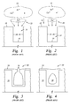
- Figure 1 illustrates a traditional, i.e., non-HDP, PVD processing environment wherein no bias is supplied to the substrate 10 by an external power generator.
- the directionality of the ions 14 is determined primarily by the ejection profile of material (usually atoms) from the target and by the inelastic collisions with other particles in the chamber, such as Ar ions which are provided in a plasma.
- the angular distribution 22 of the ions 14 in Figure 1 typically results in little deposition on the bottom 18 of the via 16 and an increasingly thinner sidewall thickness as the feature bottom 18 is approached due to a large proportion of the ions 14 striking the substrate 10 at oblique angles.
- Figure 2 illustrates the processing environment in a HDP-PVD process wherein the angular distribution of the ions 14 is influenced by the electrical field E due to an applied or a self-bias at the surface of the substrate.
- the electric field E is oriented perpendicular to the substrate 10 and the positively charged ions 14 travel along a trajectory parallel to the electric field E toward the bottom 18 of the via 16.
- the angular distribution 24 of the ions 14 in Figure 2 typically results in moderate to low deposition on the sidewalls 20 and high to moderate deposition on the bottom 18 than is possible without the bias.
- the distribution 24 exhibits a tighter pattern indicating more directionality parallel to the electric field E.
- Faceting refers to a phenomenon whereby the comers of features is partially etched by charged particles which may include ions from the plasma gas. Faceting can be undesirable because deformations of the device geometry can negatively affect subsequent processes such as electroplating. Additionally, faceting can lead to restricted feature openings and eventually to the formation of voids.
- Resputtering refers to the removal of deposited material from the substrate by the action of the impinging ions. Resputtering can be undesirable because of the potential for overhangs, i.e., relatively thicker portions of material near the opening of the features.
- the charged particles can gain enough kinetic energy to resputter a portion of the deposited material.
- the material is re-sputtered from the edges of the device features, such as vias, and from the fields of the substrate, which are the upper planar areas of the substrate formed between the features.
- the re-sputtered material then re-deposits on other areas of the substrate. While some degree of resputtering can be desirable, a problem arises when the re-sputtered material is non-uniformly re-deposited on other portions of the device features resulting in non-uniform device geometries.
- Figure 3 is a cross section of a via 30 formed in a substrate 32 having a layer 34 formed thereon, which may be a barrier layer or a seed layer for example.
- Conventional PVD and HDP-PVD processes produce overhangs 36 which restrict the via 30.
- the overhangs 36 are shown as portions of the deposited layer 34 at the upper end of the via 30 which are relatively thicker compared to the other portions of the layer 34 due to greater deposition at those locations on the via 30.
- the overhangs 36 bridge the entry to the via 30 and a void 38 is formed, as shown in Figure 4, which leads to defective devices. Void formation is also a problem resulting from faceting because the etched material can redeposit to restrict the feature opening.
- the present invention generally provides an apparatus and method for depositing a conformal layer on device features in a plasma chamber using sputtered ionized material.
- a chamber having a target, a substrate support member and a magnetic field generator to ionize the target material is provided.
- the target comprises the material to be sputtered by a plasma formed adjacent to the target during processing.
- the magnetic field generator may be one or more single-turn or multi-turn coils adapted to ionize the sputtered material.
- the invention provides methods and apparatus adapted to affect the angular distribution of ions present in the chamber.
- a modulated signal is provided to the support member during processing.
- the modulated signal includes a negative voltage portion and a zero voltage portion.
- the waveform of the signal may be modulated.
- modulated signals are provided to the target and the support member.
- the modulated signal supplied to the support member includes a negative voltage portion and a zero voltage portion.
- the modulated signal to the target is pulsed between a negative voltage portion and a zero voltage portion.
- the waveform of the signals may be modulated.
- Figure 1 is a cross section of a substrate having a via formed therein and illustrates a cosine distribution.
- Figure 2 is a cross section of a substrate having a via formed therein and illustrates an over-cosine distribution.
- Figure 3 is a cross section of a substrate illustrating the formation of overhangs.
- Figure 4 is a cross section of a substrate illustrating the formation of a void.
- Figure 5 is a cross section of a simplified processing chamber of the invention using a coil.
- Figure 6 is a schematic illustration of a controller used to control the processing system shown in Figure 5.
- Figure 7 is a graphical illustration of a pulsed output signal from a waveform generator.
- Figure 8 is a graphical illustration of a pulsed output signal from an RF power supply coupled to the waveform generator.
- Figure 9 is a graphical illustration of a pulsed bias waveform on a substrate.
- Figure 10 is a graphical illustration of a pulsed induced voltage waveform on the substrate.
- Figure 11 is a graphical illustration of a constant voltage signal to a target.
- Figure 12 is a cross section of a substrate having a via formed therein and illustrates an over-cosine distribution as a result of modulating a signal to the substrate.
- Figure 13 is a cross section of a substrate having a via formed therein and illustrates a cosine distribution as a result of modulating a signal to the substrate.
- Figures 14A-D are a series of cross sectional views of a substrate having a via formed therein and illustrates the effects of signal modulation on deposition in the via.
- Figure 15 is a graphical illustration of a pulsed signal to a target.
- Figure 16 is a graphical illustration of a pulsed induced voltage waveform on a substrate.
- Figure 17 is a cross section of a substrate having a via formed therein and illustrates a cosine distribution as a result of modulating a signal to the substrate.
- Figure 18 is a cross section of a substrate having a via formed therein and illustrates an over-cosine distribution as a result of modulating a signal to the substrate.
- Figures 19A-D are a series of cross sectional views of a substrate having a via formed therein and illustrates the effects of signal modulation on deposition in the via.
- Figures 20-22 illustrate varying waveforms output from a signal source to a support member.
- the embodiments described below preferably use a modified ionized metal plasma (IMP) process that can be carried out using process equipment, such as an Endura® platform, available from Applied Materials, Inc., located in Santa Clara, California with modifications as described below.
- the equipment preferably includes an integrated platform having a preclean chamber, an IMP-PVD barrier layer chamber, a PVD chamber, an IMP-PVD seed layer chamber, and a CVD chamber.
- One ion metal plasma (IMP) processing chamber known as an IMP VECTRATM chamber is available from Applied Materials, Inc., of Santa Clara, California.
- FIG. 5 is a schematic cross-sectional view of an IMP chamber 100 according to the present invention.
- the chamber 100 includes walls 101, lid 102, and bottom 103.
- a target 104 comprising the material to be sputtered is mounted to the lid 102 and disposed in the chamber 100 to define an upper boundary to a processing region 107.
- Magnets 106 are disposed behind the lid 102 and are part of a rotatable magnetron which trap electrons during operation and increase the density of a plasma adjacent to the target 104.
- a substrate support member 112 is movably disposed in the chamber 100 and in a raised processing position defines the lower boundary to the processing region 107.
- the substrate support member 112 provides an upper support surface 105 for supporting a substrate 110.
- Lift fingers 120 are vertically movably disposed in the substrate support 112 to assist in positioning the substrate onto the upper surface 105. Actuation of the lift fingers 120 is enabled by an elevator plate 116 and actuator 118.
- the support member 112 is mounted on a stem 109 connected to a motor assembly 114 that raises and lowers the substrate support 112 between a lowered loading/unloading position and the raised processing position.
- An opening 108 in the chamber 100 provides access for a robot (not shown) to deliver and retrieve substrates 110 to and from the chamber 100 while the substrate support member 112 is in the lowered loading/unloading position.
- a coil 122 is mounted in the chamber 100 between the substrate support member 112 and the target 104 and provides magnetic fields in the chamber 100 during processing to assist in generating and maintaining a plasma between the target 104 and substrate 110.
- the magnetic fields produced by the coil 122 induce currents in the plasma to produce a denser plasma which, in turn, ionizes the material sputtered from the target 104. At least a portion of the ionized material is then deposited on the substrate 110.
- the chamber 100 includes a process kit comprising a process shield 128 and a shadow ring 129.
- the process shield 128 is annular member suspended from the lid 102 between the coil 122 and the body 101.
- An upwardly turned wall 131 of the process shield 128 is adapted to support the shadow ring 129 while the support member 112 is in a lowered position.
- the process shield is preferably coupled to ground.
- One or more plasma gases are supplied to the chamber 100 through a gas inlet 136 from gas sources 138, 140 as metered by respective mass flow controllers 142, 144.
- a vacuum system 146 is connected to the chamber 100 at an exhaust port 148 to exhaust the chamber 100 and maintain the desired pressure in the chamber 100.
- the vacuum system 146 includes a cryopump and a roughing pump and is capable of sustaining a base pressure of about 10 -8 mTorr.
- a first signal generator 150 coupled to the target 104 provides a signal thereto.
- the first signal generator 150 includes a power supply 130 and a waveform modulator 152.
- the power supply 130 is preferably a DC power supply, in another embodiment an RF power supply may be used.
- current from the power supply 130 to the target 104 is controlled by a switch 154.
- a second signal generator 156 provides a modulated signal, preferably RF or DC, to the substrate support member 112 to bias the substrate 110 disposed thereon during processing.
- the second signal generator 156 preferably includes a power supply 134, shown here as an RF power source, and a waveform modulator 158.
- Both waveform modulators 152 and 158 include circuitry adapted for the modulation of the waveform, frequency and amplitude of output signals.
- a third power supply 132 supplies electrical power in the megahertz range to the coil 122 to increase the density of the plasma.
- the operation of the chamber 100 and the various related components are preferably controlled by a controller 149.
- the controller 149 generates signals that control the operation of both signal generators 150, 156 as required to perform the processes of the invention described below.
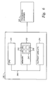
- a schematic representation of the controller is shown in Figure 6.
- the controller 149 comprises a bus line 260 coupling a central processing unit (CPU) 250, a memory 252, and support circuits 254 for the CPU 250.
- the CPU 250 may be any general purpose computer processor that can be used in an industrial setting for controlling various chambers and subprocessors.
- the support circuits 254 are coupled to the CPU 250 for supporting the processor in a conventional manner. These circuits include cache, power supplies, clock circuits, input/output circuitry and subsystems, and the like.
- the memory 252, or computer-readable medium, is coupled to the CPU 250 and may be one or more of readily available memory such as random access memory (RAM), read only memory (ROM), floppy disk drive, hard disk, or any other form of digital storage, local or remote.
- RAM random access memory
- ROM read only memory
- floppy disk drive hard disk
- hard disk any other form of digital storage, local or remote.
- a deposition process is generally stored in the memory 252, typically as a software routine 256, or program product.
- the software routine 256 may also be stored and/or executed by a second CPU (not shown) that is remotely located from the hardware being controlled by the CPU 250.
- the software routine 256 includes multiple subroutines 258 each of which are adapted to perform the various operations described below.
- a robot delivers a substrate 110 to the chamber 100 through the opening 108.
- Positioning of the substrate 110 onto the upper surface 105 is accomplished by raising the lift fingers 120, using the actuator 118 and elevator plate 116, to contact the lower surface of the substrate 110.
- the substrate support 112 is then raised while holding the lift fingers 120 in place, thereby causing the substrate 110 to be lowered onto the upper surface 105.
- the robot retracts from the chamber 100 and the opening 108 is sealed.
- the substrate support member 112 then raises the substrate 110 into a processing position. During the upward movement of the support member 112 the shadow ring 129 is lifted from the process shield 128.
- the shadow ring 129 covers a perimeter portion (a few millimeters) of the substrate 110.
- the distance between the target 104 and the substrate support member 112 in a raised processing position is about 90-160mm for a 200mm chamber operating between about 10mTorr and 70mTorr.
- One or more plasma gases are then introduced into the chamber 100 from the gas sources 138, 140 to stabilize the chamber 100 at a processing pressure.
- the magnets 106 which comprises components of a magnetron, then facilitate the formation of a plasma adjacent the target 104 and the first signal generator 150 provides a bias which attracts the charged particles of the plasma toward the target 104 to cause sputtering therefrom.
- the coil 122 is energized by the third signal generator 132 and operates to increase the density of the plasma, thereby facilitating ionization of sputtered target material. A portion of the ions formed from the sputtered target material continue to traverse the processing region 107 between the target 104 and the support member 112 and deposit on the substrate 110. Deposition onto the substrate 110 is enhanced by a bias on the substrate 110 provided by the signal generator 156. The biases to the target 104 and support member 112 are controlled according to the processes described in detail below.
- the substrate support member 112 is lowered to a loading/unloading position.
- the robot is then extended into the chamber 100 through the opening 108 and the substrate 110 is placed on the robot for removal from the chamber 100 and delivery to a subsequent location.
- Subsequent locations include various processing chambers, such as electroplating chambers, where the substrate 110 undergoes additional processing.
- the directionality of the material sputtered from the target 104 during processing is determined, in part, by the voltage drop between the plasma and the substrate 110 due to the applied or self-bias on the substrate 110.
- the voltage drop occurs in a region known as the sheath and effects an electrical field perpendicular to the substrate 110 which provides directionality of the ionized target material toward the substrate 110, thereby enhancing bottom coverage (while relatively reducing sidewall coverage) of the device feature.
- the invention modulates one or both of the bias on the substrate 110 and the bias on the target 104.
- Good step coverage on the device features of the substrate 110 is achieved by ensuring the proper proportions of bottom coverage and sidewall coverage.
- the bias signal provided to the support member 112 is modulated in various manners to achieve greater control over the deposition of a film on the substrate 110.
- the signal attributes to be controlled by the invention are waveform, frequency and amplitude. While the following embodiments are described with reference to the particular devices described above with reference to Figure 5, persons skilled in the art will recognize alternative apparatus and techniques of practicing the invention.
- a deposition process is accomplished in two phases wherein the bias to the support member 112 is pulsed between a negative voltage (phase I) and zero (0) voltage (phase II) while the voltage to target 104 is held constant.
- phase I negative voltage
- phase II zero (0) voltage
- the controller 149 transmits a corresponding signal to the waveform generator 158 which outputs the desired waveform to the power supply 134.
- the output of the signal generator 156 is then applied to the support member 112.
- Application of the signal from the signal generator 156 induces a voltage (Vdc) on the support member 112.
- the bias may be applied directly to the substrate 110. In cases where the substrate 110 comprises a non-conductive material, the bias voltage is capacitively coupled to the substrate 110.
- FIG. 7 shows the waveform 180 supplied from the waveform generator 158 to the power supply 134.
- the waveform 180 carries the information regarding the desired shape, voltage and frequency of the signal to be applied to the support member 110.
- the waveform 180 is a pulsed square wave comprising periodic power pulses 182.
- the waveform 180 includes a first phase wherein a pulse 182 is supplied to power supply 134 and a second phase wherein no signal is provided.
- the waveform 180 is converted into a corresponding output signal 184 of the desired shape, voltage, and frequency which is then supplied to the substrate support member 112.
- the resulting output signal 184 from the power supply 134 has a first portion (phase I) which varies inside an envelope 186 between a negative and positive voltage and a second portion (phase II) at zero volts.
- the signal during the second portion is a RF signal having a frequency of 13.56 MHz, however, other frequencies may be used.
- the signal generator 156 produces a pulsed output, thereby only periodically providing a bias to the support member 112.
- the output signal 184 has a pulse width t 1 (defining phase I) and a period T 1 .
- the resulting bias waveform 200 on the substrate 110 is shown in Figure 9 and illustrates that the output signal 184 from the signal generator 156 experiences a negative voltage shift.
- This shift occurs in the presence of the plasma because the output signal 184 during phase II is a RF signal which varies with time.
- electrons of a plasma can be alternately attracted and repulsed relative to the substrate 110 according to the RF output waveform 184 from the signal generator 156, the plasma ions are unable to respond to rapidly changing polarity of the RF signal because of their substantially larger inertia.
- the difference between ions and electrons of the plasma in their ability to respond to the changing polarity of the RF signal results in the shift.
- the quantity of the shift of the output signal 184 from the signal generator 156 is generally known as a self-bias voltage, Vdc.
- Figure 10 shows the quantity of the shift of the output signal 184 on the substrate 110.
- the resulting self-bias Vdc on the support member 112 illustrates phase I wherein a voltage is applied and phase II wherein no voltage is applied.
- the period and pulse width of Vdc is determined by the output of the signal generator 156.
- Vdc is a step function or square wave having the pulse width t 1 and the period T 1 .
- the waveform of the bias on the target 104, as determined by the first signal generator 150, is shown in Figure 11 which indicates that the target bias is held at a constant voltage throughout the process, i.e., during phase I and II. Thus, sputtering from the target 104 is constantly maintained at a substantially constant rate.
- the duty cycle, t 1 /T 1 is preferably between about 30-70% with a bias pulse width t 1 between about 1 ⁇ s to 10 seconds and a frequency (1/T 1 ) between about 0.1Hz-1MHz. More generally, a lower duty cycle (t 1 /T 1 ) results in more sidewall coverage while a higher duty cycle (t 1 /T 1 ) results in more bottom coverage, as will be described further below. It is noted that the frequency (typically 13.56 MHz) of the RF carrier signal is distinct from the frequency (1/T 1 ) at which the signal is pulsed or modulated.
- FIG. 12 is a cross section of a feature 210, such as a via or contact, formed in the substrate 110, wherein the feature 210 comprises a bottom 212 and sidewalls 214.
- the angular distribution pattern 216 of incoming ions exhibits substantial perpendicularity relative to the substrate 110 due to the negative bias Vdc on the substrate 110.
- application of the bias achieves more deposition on the bottom 212 than is possible without the bias on the substrate 110.
- phase II the current from the signal generator 156 is terminated. Without the presence of an applied bias to the substrate 110, the charged particles in the chamber 100 exhibit less directionality perpendicular to the substrate 110. A representation of the resulting distribution pattern 218 is shown in Figure 13 and indicates that the particles experience less directionality with respect to the substrate 110 and tend to strike the substrate 110 at oblique angles in greater proportions. As a result, the absence of the applied bias to the substrate 110 allows a higher percentage of ions to deposit on the sidewalls 214 than is possible with the applied bias.
- a lower duty cycle results in more sidewall coverage while a higher duty cycle results in more bottom coverage.
- This result follows because a lower duty cycle (i.e., short t 1 ) corresponds to a relatively higher percentage of phase II in the duty cycle wherein the resulting angular distribution produces more sidewall coverage.
- a higher duty cycle i.e., high t 1
- Figure 14A-D shows the progressive deposition of a material on the substrate 110.
- phase I Figures 14A and 14C
- the percentage of deposition on the bottom 212 of the feature 210 is higher
- the percentage of deposition on the sidewalls 214 is higher.
- the modulated bias on the substrate 110 can also be achieved by periodically opening and closing the switch 160 at a desired frequency while a constant current and voltage is provided by the second signal generator 156.
- the switch 160 With the switch 160 in a closed position, power is supplied to the support member 112 to induce a negative induced bias Vdc thereon as indicated by phase I in Figure 9, thereby establishing an electric field in the sheath between the plasma and the substrate 110.
- the switch 160 is subsequently opened in phase II, the Vdc is terminated, thereby substantially reducing the electric field in the sheath. Accordingly, the angular distribution pattern of ions can be modulated depending on the presence of the electric field E, as shown in Figures 12-13.
- the modulated angular distribution pattern accommodates the desired proportions of sidewall coverage and bottom coverage of a device feature.
- phase I when the switch 160 is closed, the angular distribution of the ions is an over-cosine distribution, resulting in more deposition on the bottom 212 of the feature 210.
- phase II when the switch 160 is open, the angular distribution of the ions is a cosine distribution, resulting in more deposition on the sidewalls 214 of the feature 210.
- Such an arrangement using switch 160 avoids the need for a more elaborate and expensive arrangement using the waveform modulator 158.
- a three phase approach is used to deposit material on a substrate whereby the signal to the target 104 and the support member 112 is modulated.
- the phases include a first target biasing phase (phase I), a neutral phase (phase II) and a support member biasing phase (phase III).
- the signals to the target 104 and the support member 112 are shown in Figures 15 and 16, respectively.
- phase I power is supplied from the first signal generator 150 to the target 104 while the support member 112 is electrically neutral, i.e., no power is supplied from the second signal generator 156.
- the resulting negative bias on the target 104 attracts positively charged ions adjacent the target 104 such as Ar ions which are made available from the Ar gas supplied by the plasma gas sources 142, 144.
- the Ar ions strike the target 104 and cause sputtering of material (typically atoms) therefrom.
- the power supplied to the target 104 is a pulsed signal 220 and preferably has a duty cycle of between about 10% and 50% and a pulse width t 2 of between about 0.1 ⁇ s and 10 ⁇ s and a period T 2 between about 1 ⁇ s and 100 ⁇ s.
- the pulse frequency (1/T 2 ) is between about 10KHz-1MHz.
- phase II both the target 104 and the support member 112 are electrically neutral, i.e. , no power is supplied from either of the signal generators 150, 156.
- the material sputtered from the target 104 during phase I traverses the processing region 107 between the target 104 and the substrate 112 and is ionized by the plasma in the chamber 100. A portion of the ionized material then deposits on the substrate 110 to form a film thereon.
- phase II may have a time duration between about 0.1 ⁇ s and 1 ⁇ s.
- the target 104 remains unbiased and a signal is provided to the support member 112 from the second signal generator 156.
- the power supplied to the support member 112 is a pulsed signal 222 and preferably has a duty cycle of between about 10-50% and a pulse width t 3 of about 0.1 ⁇ s and 10 ⁇ s and a period T 3 of 1-100ps seconds.
- the pulse frequency (1/T 3 ) is between about 10KHz-1MHz.
- Figures 17 and 18 illustrate the effects of modulating the target bias and the substrate bias on the material being deposited at the substrate surface.
- Figures 17-18 are cross sections of a feature 210 formed on the substrate 110 having a bottom 212 and sidewalls 214.
- the target 104 is sputtered while no bias is applied to the substrate 110.
- the distribution pattern of the ionized flux is relatively broader, such as the pattern shown in Figure 17. As a result, a higher percentage of the ions strike the substrate 110 at an oblique angle than would occur with an applied substrate bias.
- the resulting distribution pattern 230 of the ionized target flux (shown here as Cu) provides relatively more deposition on the sidewalls 214 than on the bottom 212 as compared to phase III.
- the signal supplied by the second signal generator 156 induces a negative bias on substrate 110 providing an attractive force to the ionized target flux and causing highly anisotropic deposition of the ionized material relative to the substrate 110.
- Application of the bias results in good coverage of the bottom 212 of the device feature 210 formed on the substrate 110.
- the resulting distribution pattern 232 of the ionized target flux generated during the application of a negative bias to the substrate is shown in Figure 18.
- Phase I provides a "burst" of material sputtered from the target 104.
- no material is being deposited on the substrate 110 because, although the target 104 has been sputtered, no material has yet traversed the space between the target 104 and the substrate 110 to reach the substrate 110.
- phase II the burst of material is ionized and arrives at the unbiased substrate to provide relatively more deposition on the sidewalls 214 of the features 210 ( Figure 19A and 19C).
- the ionized material continues to arrive at the substrate which is now biased to ensure relatively more deposition on the bottoms 212 of the features 210 ( Figures 19B and 19D).
- the bias on the substrate (Vdc) By modulating the bias on the substrate (Vdc) to vary the angular distribution of ions, the profile of the deposition may be controlled, thereby resulting in conformal step coverage and void-free deposition.
- This latter approach provides additional control during an ionized metal plasma deposition process and has particular utility where re-sputtering is a problem due to the bias on the substrate.
- periodic application of a negative bias to the support member 112 attracts charged particles, thereby increasing the incidence rate and momentum of the particles on the substrate 110.
- the bias allows for greater control of the directionality of the particles relative to the substrate, a sufficiently high bias can cause faceting of the features or re-sputtering of the material already formed on the substrate 110 and lead to undesirable device shapes.
- faceting and re-sputtering can be undesirable because of the potential for detrimental effects on subsequent processes and void formation.
- the process described with reference to Figures 15-19 provides a method of controlling faceting/re-sputtering and minimizing undesirable material formations in or on the device features.
- the "burst" of target material sputtered from the target 104 during phase I is given sufficient time to ionize during phase II before application of the bias to the substrate 110 in phase III.
- faceting of the feature and re-sputtering of the film by the Ar ions during phase I and II is avoided (or minimized where the substrate maintains some negative self-bias).
- the amount of material available for deposition can be controlled to avoid excessive deposition on the sidewalls of device features.
- terminating the bias to the target for a period of time ensures that a relatively higher electron temperature is maintained in the plasma.
- the inventors determined that maintaining a constant bias on the target can significantly depress the electron temperature of the plasma over time. As a result, the rate at which target flux is ionized is decreased. By modulating the target bias higher ionization efficiency is achieved.
- the present invention contemplates varying the waveform and/or amplitude to manipulate the energy and velocity of the ionized target material.
- the bias waveform of the output signal 184 provided to the substrate 110 may allow a more gradual ramping up to a peak voltage and ramping down to zero voltage.
- Figures 20-22 are illustrative of other waveforms which may produced by the signal generator 156 and applied to the substrate to induce a bias thereon.
Abstract
Description
- The present invention relates to an apparatus and method for processing substrates. Specifically, the invention relates to a method for depositing a conformal layer of material on a substrate in an ionized metal plasma process.
- Sub-quarter micron multi-level metallization represents one of the key technologies for the next generation of ultra large-scale integration (ULSI) for integrated circuits (IC). In the fabrication of semiconductor and other electronic devices, directionality of particles being deposited on a substrate is important to improve adequate in filling of electric features. As circuit densities increase, the widths of vias, contacts and other features, as well as the dielectric materials between them, decrease to 0.25 µm or less, whereas the thickness of the dielectric layer remains substantially constant. Thus, the aspect ratios for the features, i.e., the ratio of the depth to the minimum lateral dimension, increases, thereby pushing the aspect ratios of the contacts and vias to 5:1 and above. As the dimensions of the features decrease, it becomes even more important to directionally orient the flux of deposition material reaching the substrate in order to achieve conformal coverage of the feature sidewalls and bottoms.
- Conventionally, physical vapor deposition (PVD) systems have been used to deposit materials in device features formed on a substrate. PVD systems are well known in the field of semiconductor processing for forming metal films. Generally, a power supply connected to a processing chamber creates an electrical potential between a target and a substrate support member within the chamber and generates a plasma of a processing gas in the region between the target and substrate support member. Ions from the plasma bombard the negatively biased target and sputter material from the target which then deposits onto a substrate positioned on the substrate support member. However, while such processes have achieved good results for lower aspect ratios, conformal coverage becomes difficult to achieve with increasing aspect ratios. In particular, it has been shown that coverage (i.e., deposited film thickness) of the bottoms of the vias decreases with increasing aspect ratios.
- One process capable of providing greater directionality to particles is ionized metal plasma-physical vapor deposition (IMP-PVD), also known as high density physical vapor deposition (HDP-PVD). Initially, a plasma is generated by introducing a gas, such as helium or argon, into the chamber and then coupling energy into the chamber via a biased target to ionize the gas. A coil positioned proximate the processing region of the chamber produces an electromagnetic field which induces currents in the plasma resulting in an inductively-coupled medium/high density plasma between a target and a susceptor on which a substrate is placed for processing. The ions and electrons in the plasma are accelerated toward the target by a bias applied to the target causing the sputtering of material from the target by momentum transfer. A portion of the sputtered metal flux is then ionized by the plasma to produce metal ions in the case where the target comprises a metal. An electric field due to an applied or self-bias develops in the boundary layer, or sheath, between the plasma and the substrate that accelerates the metal ions towards the substrate in a vector parallel to the electric field and perpendicular to the substrate surface. The bias energy is preferably controlled by the application of power, such as RF or DC power, to the susceptor to attract the sputtered target ions in a highly directionalized manner to the surface of the substrate to fill the features formed on the substrate.
- One of the problems with HDP-PVD processes is the inability to achieve conformal step coverage in the increasingly smaller device features. Conformal coverage of the bottom and sidewalls of the features is needed to optimize subsequent processes such as electroplating. Electroplating requires conformal barrier and seed layers within the device features in order to ensure uniform filling of the feature. While conventional HDP-PVD achieves good bottom coverage due to the directionality of the ions provided by the bias on the substrate, the sidewall coverage can be less than conformal. This result is caused in part by the induced high directionality of ions towards the bottom of the features with little directionality toward the sidewalls.
- The effects of a bias on a substrate can be described with reference to Figures 1-2 which illustrate the direction of
metal ions 14 entering avia 16 formed on asubstrate 10. Figure 1 illustrates a traditional, i.e., non-HDP, PVD processing environment wherein no bias is supplied to thesubstrate 10 by an external power generator. In this configuration, the directionality of theions 14 is determined primarily by the ejection profile of material (usually atoms) from the target and by the inelastic collisions with other particles in the chamber, such as Ar ions which are provided in a plasma. Theangular distribution 22 of theions 14 in Figure 1 typically results in little deposition on thebottom 18 of thevia 16 and an increasingly thinner sidewall thickness as thefeature bottom 18 is approached due to a large proportion of theions 14 striking thesubstrate 10 at oblique angles. - Figure 2 illustrates the processing environment in a HDP-PVD process wherein the angular distribution of the
ions 14 is influenced by the electrical field E due to an applied or a self-bias at the surface of the substrate. The electric field E is oriented perpendicular to thesubstrate 10 and the positively chargedions 14 travel along a trajectory parallel to the electric field E toward thebottom 18 of thevia 16. Theangular distribution 24 of theions 14 in Figure 2 typically results in moderate to low deposition on thesidewalls 20 and high to moderate deposition on thebottom 18 than is possible without the bias. As compared to theangular distribution 22 of Figure 1, thedistribution 24 exhibits a tighter pattern indicating more directionality parallel to the electric field E. - Where the electric field E due to the applied bias on the
substrate 10 is sufficiently strong, faceting and/or substantial resputtering can occur. Faceting refers to a phenomenon whereby the comers of features is partially etched by charged particles which may include ions from the plasma gas. Faceting can be undesirable because deformations of the device geometry can negatively affect subsequent processes such as electroplating. Additionally, faceting can lead to restricted feature openings and eventually to the formation of voids. Resputtering refers to the removal of deposited material from the substrate by the action of the impinging ions. Resputtering can be undesirable because of the potential for overhangs, i.e., relatively thicker portions of material near the opening of the features. Under the influence of the bias, the charged particles can gain enough kinetic energy to resputter a portion of the deposited material. In particular, the material is re-sputtered from the edges of the device features, such as vias, and from the fields of the substrate, which are the upper planar areas of the substrate formed between the features. The re-sputtered material then re-deposits on other areas of the substrate. While some degree of resputtering can be desirable, a problem arises when the re-sputtered material is non-uniformly re-deposited on other portions of the device features resulting in non-uniform device geometries. - The results of the resputtering are illustrated by Figures 3 and 4. Figure 3 is a cross section of a
via 30 formed in asubstrate 32 having alayer 34 formed thereon, which may be a barrier layer or a seed layer for example. Conventional PVD and HDP-PVD processes produceoverhangs 36 which restrict thevia 30. Theoverhangs 36 are shown as portions of the depositedlayer 34 at the upper end of thevia 30 which are relatively thicker compared to the other portions of thelayer 34 due to greater deposition at those locations on thevia 30. During continued deposition, theoverhangs 36 bridge the entry to thevia 30 and avoid 38 is formed, as shown in Figure 4, which leads to defective devices. Void formation is also a problem resulting from faceting because the etched material can redeposit to restrict the feature opening. - Therefore, there is a need to provide a technique for depositing a layer conformally over the surface of features, particularly sub-half micron and higher aspect ratio features.
- The present invention generally provides an apparatus and method for depositing a conformal layer on device features in a plasma chamber using sputtered ionized material. In one embodiment, a chamber having a target, a substrate support member and a magnetic field generator to ionize the target material is provided. The target comprises the material to be sputtered by a plasma formed adjacent to the target during processing. The magnetic field generator may be one or more single-turn or multi-turn coils adapted to ionize the sputtered material. The invention provides methods and apparatus adapted to affect the angular distribution of ions present in the chamber.
- In one aspect of the invention, a modulated signal is provided to the support member during processing. Preferably, the modulated signal includes a negative voltage portion and a zero voltage portion. In one embodiment, the waveform of the signal may be modulated.
- In another aspect of the invention, modulated signals are provided to the target and the support member. Preferably, the modulated signal supplied to the support member includes a negative voltage portion and a zero voltage portion. In one embodiment, the modulated signal to the target is pulsed between a negative voltage portion and a zero voltage portion. In one embodiment, the waveform of the signals may be modulated.
- So that the manner in which the above recited features, advantages and objects of the present invention are attained and can be understood in detail, a more particular description of the invention, briefly summarized above, may be had by reference to the embodiments thereof which are illustrated in the appended drawings.
- It is to be noted, however, that the appended drawings illustrate only typical embodiments of this invention and are therefore not to be considered limiting of its scope, for the invention may admit to other equally effective embodiments.
- Figure 1 is a cross section of a substrate having a via formed therein and illustrates a cosine distribution.
- Figure 2 is a cross section of a substrate having a via formed therein and illustrates an over-cosine distribution.
- Figure 3 is a cross section of a substrate illustrating the formation of overhangs.
- Figure 4 is a cross section of a substrate illustrating the formation of a void.
- Figure 5 is a cross section of a simplified processing chamber of the invention using a coil.
- Figure 6 is a schematic illustration of a controller used to control the processing system shown in Figure 5.
- Figure 7 is a graphical illustration of a pulsed output signal from a waveform generator.
- Figure 8 is a graphical illustration of a pulsed output signal from an RF power supply coupled to the waveform generator.
- Figure 9 is a graphical illustration of a pulsed bias waveform on a substrate.
- Figure 10 is a graphical illustration of a pulsed induced voltage waveform on the substrate.
- Figure 11 is a graphical illustration of a constant voltage signal to a target.
- Figure 12 is a cross section of a substrate having a via formed therein and illustrates an over-cosine distribution as a result of modulating a signal to the substrate.
- Figure 13 is a cross section of a substrate having a via formed therein and illustrates a cosine distribution as a result of modulating a signal to the substrate.
- Figures 14A-D are a series of cross sectional views of a substrate having a via formed therein and illustrates the effects of signal modulation on deposition in the via.
- Figure 15 is a graphical illustration of a pulsed signal to a target.
- Figure 16 is a graphical illustration of a pulsed induced voltage waveform on a substrate.
- Figure 17 is a cross section of a substrate having a via formed therein and illustrates a cosine distribution as a result of modulating a signal to the substrate.
- Figure 18 is a cross section of a substrate having a via formed therein and illustrates an over-cosine distribution as a result of modulating a signal to the substrate.
- Figures 19A-D are a series of cross sectional views of a substrate having a via formed therein and illustrates the effects of signal modulation on deposition in the via.
- Figures 20-22 illustrate varying waveforms output from a signal source to a support member.
- The embodiments described below preferably use a modified ionized metal plasma (IMP) process that can be carried out using process equipment, such as an Endura® platform, available from Applied Materials, Inc., located in Santa Clara, California with modifications as described below. The equipment preferably includes an integrated platform having a preclean chamber, an IMP-PVD barrier layer chamber, a PVD chamber, an IMP-PVD seed layer chamber, and a CVD chamber. One ion metal plasma (IMP) processing chamber, known as an IMP VECTRA™ chamber is available from Applied Materials, Inc., of Santa Clara, California.
- Figure 5 is a schematic cross-sectional view of an
IMP chamber 100 according to the present invention. Thechamber 100 includeswalls 101,lid 102, andbottom 103. Atarget 104 comprising the material to be sputtered is mounted to thelid 102 and disposed in thechamber 100 to define an upper boundary to aprocessing region 107.Magnets 106 are disposed behind thelid 102 and are part of a rotatable magnetron which trap electrons during operation and increase the density of a plasma adjacent to thetarget 104. - A
substrate support member 112 is movably disposed in thechamber 100 and in a raised processing position defines the lower boundary to theprocessing region 107. Thesubstrate support member 112 provides anupper support surface 105 for supporting asubstrate 110. Liftfingers 120 are vertically movably disposed in thesubstrate support 112 to assist in positioning the substrate onto theupper surface 105. Actuation of thelift fingers 120 is enabled by anelevator plate 116 andactuator 118. Thesupport member 112 is mounted on astem 109 connected to amotor assembly 114 that raises and lowers thesubstrate support 112 between a lowered loading/unloading position and the raised processing position. Anopening 108 in thechamber 100 provides access for a robot (not shown) to deliver and retrievesubstrates 110 to and from thechamber 100 while thesubstrate support member 112 is in the lowered loading/unloading position. - A
coil 122 is mounted in thechamber 100 between thesubstrate support member 112 and thetarget 104 and provides magnetic fields in thechamber 100 during processing to assist in generating and maintaining a plasma between thetarget 104 andsubstrate 110. The magnetic fields produced by thecoil 122 induce currents in the plasma to produce a denser plasma which, in turn, ionizes the material sputtered from thetarget 104. At least a portion of the ionized material is then deposited on thesubstrate 110. - The
chamber 100 includes a process kit comprising aprocess shield 128 and ashadow ring 129. Theprocess shield 128 is annular member suspended from thelid 102 between thecoil 122 and thebody 101. An upwardly turnedwall 131 of theprocess shield 128 is adapted to support theshadow ring 129 while thesupport member 112 is in a lowered position. To provide a return path for RF currents in thechamber 100 the process shield is preferably coupled to ground. - One or more plasma gases are supplied to the
chamber 100 through agas inlet 136 fromgas sources mass flow controllers vacuum system 146 is connected to thechamber 100 at anexhaust port 148 to exhaust thechamber 100 and maintain the desired pressure in thechamber 100. Preferably, thevacuum system 146 includes a cryopump and a roughing pump and is capable of sustaining a base pressure of about 10-8mTorr. - Multiple signal generators/power supplies are used in the
chamber 100. Afirst signal generator 150 coupled to thetarget 104 provides a signal thereto. Preferably, thefirst signal generator 150 includes apower supply 130 and awaveform modulator 152. While thepower supply 130 is preferably a DC power supply, in another embodiment an RF power supply may be used. Optionally, current from thepower supply 130 to thetarget 104 is controlled by aswitch 154. Asecond signal generator 156 provides a modulated signal, preferably RF or DC, to thesubstrate support member 112 to bias thesubstrate 110 disposed thereon during processing. Thesecond signal generator 156 preferably includes apower supply 134, shown here as an RF power source, and awaveform modulator 158. Optionally, current from thepower supply 134 to thetarget 104 is controlled by aswitch 160. Bothwaveform modulators third power supply 132 supplies electrical power in the megahertz range to thecoil 122 to increase the density of the plasma. - The operation of the
chamber 100 and the various related components are preferably controlled by acontroller 149. In particular, thecontroller 149 generates signals that control the operation of bothsignal generators controller 149 comprises a bus line 260 coupling a central processing unit (CPU) 250, amemory 252, and supportcircuits 254 for theCPU 250. TheCPU 250 may be any general purpose computer processor that can be used in an industrial setting for controlling various chambers and subprocessors. Thesupport circuits 254 are coupled to theCPU 250 for supporting the processor in a conventional manner. These circuits include cache, power supplies, clock circuits, input/output circuitry and subsystems, and the like. Thememory 252, or computer-readable medium, is coupled to theCPU 250 and may be one or more of readily available memory such as random access memory (RAM), read only memory (ROM), floppy disk drive, hard disk, or any other form of digital storage, local or remote. A deposition process is generally stored in thememory 252, typically as asoftware routine 256, or program product. Thesoftware routine 256 may also be stored and/or executed by a second CPU (not shown) that is remotely located from the hardware being controlled by theCPU 250. Thesoftware routine 256 includesmultiple subroutines 258 each of which are adapted to perform the various operations described below. - In operation, a robot delivers a
substrate 110 to thechamber 100 through theopening 108. Positioning of thesubstrate 110 onto theupper surface 105 is accomplished by raising thelift fingers 120, using theactuator 118 andelevator plate 116, to contact the lower surface of thesubstrate 110. Thesubstrate support 112 is then raised while holding thelift fingers 120 in place, thereby causing thesubstrate 110 to be lowered onto theupper surface 105. After depositing thesubstrate 110 unto theupper surface 105 of thesupport member 112 the robot retracts from thechamber 100 and theopening 108 is sealed. Thesubstrate support member 112 then raises thesubstrate 110 into a processing position. During the upward movement of thesupport member 112 theshadow ring 129 is lifted from theprocess shield 128. During processing, theshadow ring 129 covers a perimeter portion (a few millimeters) of thesubstrate 110. Preferably, the distance between thetarget 104 and thesubstrate support member 112 in a raised processing position is about 90-160mm for a 200mm chamber operating between about 10mTorr and 70mTorr. One or more plasma gases are then introduced into thechamber 100 from thegas sources chamber 100 at a processing pressure. Themagnets 106, which comprises components of a magnetron, then facilitate the formation of a plasma adjacent thetarget 104 and thefirst signal generator 150 provides a bias which attracts the charged particles of the plasma toward thetarget 104 to cause sputtering therefrom. Thecoil 122 is energized by thethird signal generator 132 and operates to increase the density of the plasma, thereby facilitating ionization of sputtered target material. A portion of the ions formed from the sputtered target material continue to traverse theprocessing region 107 between thetarget 104 and thesupport member 112 and deposit on thesubstrate 110. Deposition onto thesubstrate 110 is enhanced by a bias on thesubstrate 110 provided by thesignal generator 156. The biases to thetarget 104 andsupport member 112 are controlled according to the processes described in detail below. - Following the deposition cycle, the
substrate support member 112 is lowered to a loading/unloading position. The robot is then extended into thechamber 100 through theopening 108 and thesubstrate 110 is placed on the robot for removal from thechamber 100 and delivery to a subsequent location. Subsequent locations include various processing chambers, such as electroplating chambers, where thesubstrate 110 undergoes additional processing. - The directionality of the material sputtered from the
target 104 during processing is determined, in part, by the voltage drop between the plasma and thesubstrate 110 due to the applied or self-bias on thesubstrate 110. The voltage drop occurs in a region known as the sheath and effects an electrical field perpendicular to thesubstrate 110 which provides directionality of the ionized target material toward thesubstrate 110, thereby enhancing bottom coverage (while relatively reducing sidewall coverage) of the device feature. In order to achieve improved sidewall coverage, the invention modulates one or both of the bias on thesubstrate 110 and the bias on thetarget 104. Good step coverage on the device features of thesubstrate 110 is achieved by ensuring the proper proportions of bottom coverage and sidewall coverage. - In one aspect of the invention, the bias signal provided to the
support member 112 is modulated in various manners to achieve greater control over the deposition of a film on thesubstrate 110. In general, the signal attributes to be controlled by the invention are waveform, frequency and amplitude. While the following embodiments are described with reference to the particular devices described above with reference to Figure 5, persons skilled in the art will recognize alternative apparatus and techniques of practicing the invention. - In a first embodiment of the invention, a deposition process is accomplished in two phases wherein the bias to the
support member 112 is pulsed between a negative voltage (phase I) and zero (0) voltage (phase II) while the voltage to target 104 is held constant. This may be done using thecontroller 149 and executing theappropriate subroutine 258 stored in memory 252 (shown in Figure 6). According to the particular file executed, thecontroller 149 transmits a corresponding signal to thewaveform generator 158 which outputs the desired waveform to thepower supply 134. The output of thesignal generator 156 is then applied to thesupport member 112. Application of the signal from thesignal generator 156 induces a voltage (Vdc) on thesupport member 112. Where thesubstrate 110 comprises a conductive material, or layer of material, the bias may be applied directly to thesubstrate 110. In cases where thesubstrate 110 comprises a non-conductive material, the bias voltage is capacitively coupled to thesubstrate 110. - The output of the
waveform generator 158, thesignal generator 156 and the bias waveform on thesubstrate 110 disposed on thesupport member 112 are shown in Figures 7,8 and 9 respectively. Figure 7 shows thewaveform 180 supplied from thewaveform generator 158 to thepower supply 134. Thewaveform 180 carries the information regarding the desired shape, voltage and frequency of the signal to be applied to thesupport member 110. Thewaveform 180 is a pulsed square wave comprisingperiodic power pulses 182. Thus, thewaveform 180 includes a first phase wherein apulse 182 is supplied topower supply 134 and a second phase wherein no signal is provided. At thepower supply 134, thewaveform 180 is converted into acorresponding output signal 184 of the desired shape, voltage, and frequency which is then supplied to thesubstrate support member 112. As shown in Figure 8, the resulting output signal 184 from thepower supply 134 has a first portion (phase I) which varies inside anenvelope 186 between a negative and positive voltage and a second portion (phase II) at zero volts. Preferably, the signal during the second portion is a RF signal having a frequency of 13.56 MHz, however, other frequencies may be used. Thus, thesignal generator 156 produces a pulsed output, thereby only periodically providing a bias to thesupport member 112. Theoutput signal 184 has a pulse width t1 (defining phase I) and a period T1. - The resulting
bias waveform 200 on thesubstrate 110 is shown in Figure 9 and illustrates that theoutput signal 184 from thesignal generator 156 experiences a negative voltage shift. This shift occurs in the presence of the plasma because theoutput signal 184 during phase II is a RF signal which varies with time. While electrons of a plasma can be alternately attracted and repulsed relative to thesubstrate 110 according to theRF output waveform 184 from thesignal generator 156, the plasma ions are unable to respond to rapidly changing polarity of the RF signal because of their substantially larger inertia. The difference between ions and electrons of the plasma in their ability to respond to the changing polarity of the RF signal results in the shift. - The quantity of the shift of the
output signal 184 from thesignal generator 156 is generally known as a self-bias voltage, Vdc. Figure 10 shows the quantity of the shift of theoutput signal 184 on thesubstrate 110. The resulting self-bias Vdc on thesupport member 112 illustrates phase I wherein a voltage is applied and phase II wherein no voltage is applied. The period and pulse width of Vdc is determined by the output of thesignal generator 156. Thus, Vdc is a step function or square wave having the pulse width t1 and the period T1. - The waveform of the bias on the
target 104, as determined by thefirst signal generator 150, is shown in Figure 11 which indicates that the target bias is held at a constant voltage throughout the process, i.e., during phase I and II. Thus, sputtering from thetarget 104 is constantly maintained at a substantially constant rate. - By controlling the duty cycle of the
bias waveform 200 applied to thesubstrate 110, the desired proportions of bottom and sidewall coverage of the features formed in thesubstrate 110 are possible. The duty cycle, t1/T1, is preferably between about 30-70% with a bias pulse width t1 between about 1µs to 10 seconds and a frequency (1/T1) between about 0.1Hz-1MHz. More generally, a lower duty cycle (t1/T1) results in more sidewall coverage while a higher duty cycle (t1/T1) results in more bottom coverage, as will be described further below. It is noted that the frequency (typically 13.56 MHz) of the RF carrier signal is distinct from the frequency (1/T1) at which the signal is pulsed or modulated. - In phase I, the power supplied to the
support member 112 induces the negative bias Vdc on thesubstrate 110 as illustrated graphically in Figure 9. The negative bias attracts positively charged particles, primarily the ionized metal, toward thesubstrate 110. Because the bias Vdc establishes a resulting electric field E substantially perpendicular to thesubstrate 110, the positively charged particles in theprocessing region 107 assume a trajectory substantially perpendicular to thesubstrate 110. Figure 12 is a cross section of afeature 210, such as a via or contact, formed in thesubstrate 110, wherein thefeature 210 comprises a bottom 212 andsidewalls 214. Theangular distribution pattern 216 of incoming ions, shown here as Cu ions, exhibits substantial perpendicularity relative to thesubstrate 110 due to the negative bias Vdc on thesubstrate 110. As a result, application of the bias achieves more deposition on the bottom 212 than is possible without the bias on thesubstrate 110. - In phase II, the current from the
signal generator 156 is terminated. Without the presence of an applied bias to thesubstrate 110, the charged particles in thechamber 100 exhibit less directionality perpendicular to thesubstrate 110. A representation of the resultingdistribution pattern 218 is shown in Figure 13 and indicates that the particles experience less directionality with respect to thesubstrate 110 and tend to strike thesubstrate 110 at oblique angles in greater proportions. As a result, the absence of the applied bias to thesubstrate 110 allows a higher percentage of ions to deposit on thesidewalls 214 than is possible with the applied bias. - As noted above, a lower duty cycle results in more sidewall coverage while a higher duty cycle results in more bottom coverage. This result follows because a lower duty cycle (i.e., short t1) corresponds to a relatively higher percentage of phase II in the duty cycle wherein the resulting angular distribution produces more sidewall coverage. A higher duty cycle (i.e., high t1), on the other hand, corresponds to a relatively longer phase I wherein the resulting angular distribution produces more bottom coverage.
- The effect of pulsing the bias on the
substrate 110 is illustrated in Figure 14A-D which shows the progressive deposition of a material on thesubstrate 110. During phase I (Figures 14A and 14C) the percentage of deposition on thebottom 212 of thefeature 210 is higher, while during phase II (Figures 14B and 14D) the percentage of deposition on thesidewalls 214 is higher. By modulating the substrate bias to vary the angular distribution of ions, the profile of the deposition may be controlled, thereby resulting in conformal step coverage and void-free deposition. - In an alternative embodiment, the modulated bias on the
substrate 110 can also be achieved by periodically opening and closing theswitch 160 at a desired frequency while a constant current and voltage is provided by thesecond signal generator 156. With theswitch 160 in a closed position, power is supplied to thesupport member 112 to induce a negative induced bias Vdc thereon as indicated by phase I in Figure 9, thereby establishing an electric field in the sheath between the plasma and thesubstrate 110. When theswitch 160 is subsequently opened in phase II, the Vdc is terminated, thereby substantially reducing the electric field in the sheath. Accordingly, the angular distribution pattern of ions can be modulated depending on the presence of the electric field E, as shown in Figures 12-13. The modulated angular distribution pattern, in turn, accommodates the desired proportions of sidewall coverage and bottom coverage of a device feature. During phase I, when theswitch 160 is closed, the angular distribution of the ions is an over-cosine distribution, resulting in more deposition on thebottom 212 of thefeature 210. During phase II, when theswitch 160 is open, the angular distribution of the ions is a cosine distribution, resulting in more deposition on thesidewalls 214 of thefeature 210. Such anarrangement using switch 160 avoids the need for a more elaborate and expensive arrangement using thewaveform modulator 158. - In another embodiment, a three phase approach is used to deposit material on a substrate whereby the signal to the
target 104 and thesupport member 112 is modulated. The phases include a first target biasing phase (phase I), a neutral phase (phase II) and a support member biasing phase (phase III). The signals to thetarget 104 and thesupport member 112 are shown in Figures 15 and 16, respectively. - During phase I, power is supplied from the
first signal generator 150 to thetarget 104 while thesupport member 112 is electrically neutral, i.e., no power is supplied from thesecond signal generator 156. The resulting negative bias on thetarget 104 attracts positively charged ions adjacent thetarget 104 such as Ar ions which are made available from the Ar gas supplied by theplasma gas sources target 104 and cause sputtering of material (typically atoms) therefrom. As shown in Figure 15, the power supplied to thetarget 104 is apulsed signal 220 and preferably has a duty cycle of between about 10% and 50% and a pulse width t2 of between about 0.1 µs and 10µs and a period T2 between about 1µs and 100µs. Thus, the pulse frequency (1/T2) is between about 10KHz-1MHz. - During phase II, both the
target 104 and thesupport member 112 are electrically neutral, i.e., no power is supplied from either of thesignal generators target 104 during phase I traverses theprocessing region 107 between thetarget 104 and thesubstrate 112 and is ionized by the plasma in thechamber 100. A portion of the ionized material then deposits on thesubstrate 110 to form a film thereon. In one embodiment, phase II may have a time duration between about 0.1 µs and 1 µs. - During phase III, the
target 104 remains unbiased and a signal is provided to thesupport member 112 from thesecond signal generator 156. As shown in Figure 16, the power supplied to thesupport member 112 is apulsed signal 222 and preferably has a duty cycle of between about 10-50% and a pulse width t3 of about 0.1µs and 10µs and a period T3 of 1-100ps seconds. Thus, the pulse frequency (1/T3) is between about 10KHz-1MHz. - Figures 17 and 18 illustrate the effects of modulating the target bias and the substrate bias on the material being deposited at the substrate surface. Figures 17-18 are cross sections of a
feature 210 formed on thesubstrate 110 having a bottom 212 andsidewalls 214. During phases I and II, thetarget 104 is sputtered while no bias is applied to thesubstrate 110. In the absence of an applied bias to thesubstrate 110, the distribution pattern of the ionized flux is relatively broader, such as the pattern shown in Figure 17. As a result, a higher percentage of the ions strike thesubstrate 110 at an oblique angle than would occur with an applied substrate bias. The resultingdistribution pattern 230 of the ionized target flux (shown here as Cu) provides relatively more deposition on thesidewalls 214 than on the bottom 212 as compared to phase III. During phase III, the signal supplied by thesecond signal generator 156 induces a negative bias onsubstrate 110 providing an attractive force to the ionized target flux and causing highly anisotropic deposition of the ionized material relative to thesubstrate 110. Application of the bias results in good coverage of the bottom 212 of thedevice feature 210 formed on thesubstrate 110. The resultingdistribution pattern 232 of the ionized target flux generated during the application of a negative bias to the substrate is shown in Figure 18. - The effect of the three phase pulsing method described above on deposition is illustrated in Figures 19A-D which show the progressive deposition of material on the
substrate 110. Phase I provides a "burst" of material sputtered from thetarget 104. During phase I no material is being deposited on thesubstrate 110 because, although thetarget 104 has been sputtered, no material has yet traversed the space between thetarget 104 and thesubstrate 110 to reach thesubstrate 110. In phase II, the burst of material is ionized and arrives at the unbiased substrate to provide relatively more deposition on thesidewalls 214 of the features 210 (Figure 19A and 19C). During Phase III, the ionized material continues to arrive at the substrate which is now biased to ensure relatively more deposition on thebottoms 212 of the features 210 (Figures 19B and 19D). By modulating the bias on the substrate (Vdc) to vary the angular distribution of ions, the profile of the deposition may be controlled, thereby resulting in conformal step coverage and void-free deposition. - This latter approach provides additional control during an ionized metal plasma deposition process and has particular utility where re-sputtering is a problem due to the bias on the substrate. As described with respect to each of the embodiments above, periodic application of a negative bias to the
support member 112 attracts charged particles, thereby increasing the incidence rate and momentum of the particles on thesubstrate 110. While the bias allows for greater control of the directionality of the particles relative to the substrate, a sufficiently high bias can cause faceting of the features or re-sputtering of the material already formed on thesubstrate 110 and lead to undesirable device shapes. As described above, faceting and re-sputtering can be undesirable because of the potential for detrimental effects on subsequent processes and void formation. - Because a bias to the
substrate 110 is applied only for a short period of time, the process described with reference to Figures 15-19 provides a method of controlling faceting/re-sputtering and minimizing undesirable material formations in or on the device features. The "burst" of target material sputtered from thetarget 104 during phase I is given sufficient time to ionize during phase II before application of the bias to thesubstrate 110 in phase III. Thus, faceting of the feature and re-sputtering of the film by the Ar ions during phase I and II is avoided (or minimized where the substrate maintains some negative self-bias). By simultaneously modulating the bias to thetarget 104, the amount of material available for deposition can be controlled to avoid excessive deposition on the sidewalls of device features. - Additionally, terminating the bias to the target for a period of time ensures that a relatively higher electron temperature is maintained in the plasma. The inventors determined that maintaining a constant bias on the target can significantly depress the electron temperature of the plasma over time. As a result, the rate at which target flux is ionized is decreased. By modulating the target bias higher ionization efficiency is achieved.
- While the foregoing embodiments utilize a step function waveform (i.e., the AC signal is supplied at zero or at full frequency/power), the present invention contemplates varying the waveform and/or amplitude to manipulate the energy and velocity of the ionized target material. Thus, rather than abruptly altering the angular distribution of the ionized material with square wave pulses, such as are shown in Figures 7-10 and 16, the bias waveform of the
output signal 184 provided to thesubstrate 110 may allow a more gradual ramping up to a peak voltage and ramping down to zero voltage. Figures 20-22 are illustrative of other waveforms which may produced by thesignal generator 156 and applied to the substrate to induce a bias thereon. By controlling the waveform of the signal applied to the substrate being processed, the ion directionality and, hence, the deposition profile, can be adjusted to achieve a desired result. - While the foregoing is directed to the preferred embodiment of the present invention, other and further embodiments of the invention may be devised without departing from the basic scope thereof, and the scope thereof is determined by the claims that follow.
Claims (23)
- A method of depositing a material on a substrate in a process chamber, comprising:(a) providing a first signal to a support member having the substrate disposed thereon;(b) providing a second signal to a target;(c) energizing a magnetic field generator disposed in the processing chamber; and(d) varying the first signal between a first negative voltage portion and a first zero voltage portion relative to ground.
- A method as claimed in claim 1, wherein a duty cycle of the first signal is between about 30% and about 70%.
- A method as claimed in claim 1 or claim 2, wherein a duty cycle of the second signal is between about 10% and about 50%.
- A method as claimed in any of claims 1 to 3, wherein (a) comprises supplying a radio frequency (RF) signal to the support member.
- A method as claimed in any of claims 1 to 3, wherein (a) comprises supplying a pulsed RF signal.
- A method as claimed in any of claims 1 to 5, wherein (b) comprises supplying a DC signal to the target.
- A method as claimed in any of claims 1 to 6, wherein (c) comprises energizing a coil.
- A method as claimed in any of claims 1 to 7, wherein (c) comprises supplying a RF signal to the magnetic field generator.
- A method as claimed in any of claims 1 to 7, further comprising:
(e) varying the second signal between a second negative voltage portion and a second zero voltage portion relative to ground. - A method as claimed in claim 9, wherein the second signal comprises a pulsed DC signal.
- A method as claimed in any of claims 1 to 10, further comprising:(e) supplying a gas to the chamber;(f) sputtering a material from the target; and(g) ionizing the sputtered material.
- A method as claimed in any of claims 1 to 10, further comprising:wherein (a) comprises supplying a first RF signal to the substrate, (b) comprises supplying a DC signal to the target and (c) comprises supplying a second RF signal to the magnetic field generator.(e) providing a plasma to the chamber;(f) sputtering a material from the target; and(g) ionizing the sputtered material;
- A method of depositing a material on a substrate in a process chamber, comprising:(a) supplying a plasma to the processing chamber;(b) providing a first signal of a first waveform to a support member having the substrate disposed thereon;(c) providing a second signal of a second waveform to a target;(d) energizing a coil with a RF signal;(e) varying the first signal between a first negative voltage portion and a first zero voltage portion relative to ground; and(f) varying the second signal between a second negative voltage portion and a second zero voltage portion relative to ground.
- A method as claimed in claim 13, wherein (b) comprises supplying a RF signal to the support member and (c) comprises supplying a DC signal to the target.
- A method as claimed in claim 13 or claim 14, wherein the first signal has a duty cycle of between about 30% and about 70% and has a frequency between about 0.1Hz and 1MHz.
- A method as claimed in any of claims 13 to 15, wherein the second signal has a duty cycle of between about 10% and about 50% and has a frequency between about 10KHz and 1MHz.
- A method as claimed in any of claims 13 to 16, wherein the first signal and the second signal are pulsed signals.
- A method as claimed in any of claim 13 to 16, wherein the first negative portion is provided to the support member during the second zero voltage portion.
- A method as claimed in claim 18, wherein the first signal and the second signal are pulsed signals and wherein a first pulse width of the first negative portion is less than a second pulse width of the second zero voltage portion.
- A program product, which when read and executed by one more controllers, comprises the steps of:(a) flowing a gas into a processing chamber;(b) providing a first signal to a target;(c) providing a second signal to a support member having the substrate disposed thereon;(d) energizing a coil with an RF signal;(e) varying the first signal; and(f) varying the second signal.
- A program product as claimed in claim 20, wherein (c) comprises supplying a pulsed RF signal to the support member.
- A program product as claimed in claim 20, wherein (c) comprises supplying a pulsed signal to the support member having a negative voltage portion and a zero voltage portion.
- A program product as claimed in any of claims 20 to 22, wherein (e) and (f) comprise decreasing a voltage to the target for a period of time and increasing a voltage to the support member during at least a portion of the period of time.
Applications Claiming Priority (2)
| Application Number | Priority Date | Filing Date | Title |
|---|---|---|---|
| US09/454,355 US6344419B1 (en) | 1999-12-03 | 1999-12-03 | Pulsed-mode RF bias for sidewall coverage improvement |
| US454355 | 1999-12-03 |
Publications (2)
| Publication Number | Publication Date |
|---|---|
| EP1106709A2 true EP1106709A2 (en) | 2001-06-13 |
| EP1106709A3 EP1106709A3 (en) | 2004-01-02 |
Family
ID=23804277
Family Applications (1)
| Application Number | Title | Priority Date | Filing Date |
|---|---|---|---|
| EP00310702A Withdrawn EP1106709A3 (en) | 1999-12-03 | 2000-12-01 | Pulsed-mode RF bias for side-wall coverage improvement |
Country Status (5)
| Country | Link |
|---|---|
| US (2) | US6344419B1 (en) |
| EP (1) | EP1106709A3 (en) |
| JP (1) | JP2001274115A (en) |
| KR (1) | KR20010062115A (en) |
| SG (1) | SG86450A1 (en) |
Cited By (8)
| Publication number | Priority date | Publication date | Assignee | Title |
|---|---|---|---|---|
| WO2005005684A1 (en) * | 2003-07-10 | 2005-01-20 | Biocell Aktiebolag | Work piece processing by pulsed electric discharges in solid-gas plasma |
| WO2005118905A1 (en) * | 2004-05-26 | 2005-12-15 | Tokyo Electron Limited | Method and apparatus of plasma processing |
| EP1734558A1 (en) * | 2005-06-14 | 2006-12-20 | Applied Films Corporation | System for modulating power signals to control sputtering |
| FR2904726A1 (en) * | 2006-08-07 | 2008-02-08 | Sidel Participations | METHOD AND DEVICE FOR COLD PLASMA BARRIER LAYER DEPOSITION AND MACHINE USING SUCH A DEVICE |
| WO2008071732A2 (en) * | 2006-12-12 | 2008-06-19 | Oc Oerlikon Balzers Ag | Rf substrate bias with high power impulse magnetron sputtering (hipims) |
| WO2009053479A2 (en) * | 2007-10-26 | 2009-04-30 | Oc Oerlikon Balzers Ag | Application of hipims to through silicon via metallization in three-dimensional wafer packaging |
| WO2009125189A1 (en) * | 2008-04-09 | 2009-10-15 | The University Of Sheffield | Biased plasma assisted processing |
| WO2023191835A1 (en) * | 2022-03-29 | 2023-10-05 | Applied Materials, Inc. | Electromagnet pulsing effect on pvd step coverage |
Families Citing this family (106)
| Publication number | Priority date | Publication date | Assignee | Title |
|---|---|---|---|---|
| US6344419B1 (en) * | 1999-12-03 | 2002-02-05 | Applied Materials, Inc. | Pulsed-mode RF bias for sidewall coverage improvement |
| US6913680B1 (en) * | 2000-05-02 | 2005-07-05 | Applied Materials, Inc. | Method of application of electrical biasing to enhance metal deposition |
| JP2004513221A (en) | 2000-05-23 | 2004-04-30 | アプライド マテリアルズ インコーポレイテッド | Method and apparatus for overcoming copper seed layer anomalies and adjusting surface feature size and aspect ratio |
| US6544895B1 (en) * | 2000-08-17 | 2003-04-08 | Micron Technology, Inc. | Methods for use of pulsed voltage in a plasma reactor |
| US6485572B1 (en) * | 2000-08-28 | 2002-11-26 | Micron Technology, Inc. | Use of pulsed grounding source in a plasma reactor |
| EP1470268A2 (en) * | 2000-10-03 | 2004-10-27 | Applied Materials, Inc. | Method and associated apparatus for tilting a substrate upon entry for metal deposition |
| US6703300B2 (en) * | 2001-03-30 | 2004-03-09 | The Penn State Research Foundation | Method for making multilayer electronic devices |
| US7469558B2 (en) * | 2001-07-10 | 2008-12-30 | Springworks, Llc | As-deposited planar optical waveguides with low scattering loss and methods for their manufacture |
| US6503824B1 (en) * | 2001-10-12 | 2003-01-07 | Mosel Vitelic, Inc. | Forming conductive layers on insulators by physical vapor deposition |
| US7404877B2 (en) * | 2001-11-09 | 2008-07-29 | Springworks, Llc | Low temperature zirconia based thermal barrier layer by PVD |
| US20030175142A1 (en) * | 2002-03-16 | 2003-09-18 | Vassiliki Milonopoulou | Rare-earth pre-alloyed PVD targets for dielectric planar applications |
| US6884327B2 (en) | 2002-03-16 | 2005-04-26 | Tao Pan | Mode size converter for a planar waveguide |
| US7378356B2 (en) * | 2002-03-16 | 2008-05-27 | Springworks, Llc | Biased pulse DC reactive sputtering of oxide films |
| US6911136B2 (en) * | 2002-04-29 | 2005-06-28 | Applied Materials, Inc. | Method for regulating the electrical power applied to a substrate during an immersion process |
| US7067439B2 (en) * | 2002-06-14 | 2006-06-27 | Applied Materials, Inc. | ALD metal oxide deposition process using direct oxidation |
| US8394522B2 (en) * | 2002-08-09 | 2013-03-12 | Infinite Power Solutions, Inc. | Robust metal film encapsulation |
| US8236443B2 (en) * | 2002-08-09 | 2012-08-07 | Infinite Power Solutions, Inc. | Metal film encapsulation |
| US8021778B2 (en) * | 2002-08-09 | 2011-09-20 | Infinite Power Solutions, Inc. | Electrochemical apparatus with barrier layer protected substrate |
| US8404376B2 (en) | 2002-08-09 | 2013-03-26 | Infinite Power Solutions, Inc. | Metal film encapsulation |
| US8445130B2 (en) * | 2002-08-09 | 2013-05-21 | Infinite Power Solutions, Inc. | Hybrid thin-film battery |
| US8431264B2 (en) * | 2002-08-09 | 2013-04-30 | Infinite Power Solutions, Inc. | Hybrid thin-film battery |
| US9793523B2 (en) | 2002-08-09 | 2017-10-17 | Sapurast Research Llc | Electrochemical apparatus with barrier layer protected substrate |
| US20070264564A1 (en) | 2006-03-16 | 2007-11-15 | Infinite Power Solutions, Inc. | Thin film battery on an integrated circuit or circuit board and method thereof |
| AU2003261463A1 (en) * | 2002-08-27 | 2004-03-19 | Symmorphix, Inc. | Optically coupling into highly uniform waveguides |
| US6784096B2 (en) * | 2002-09-11 | 2004-08-31 | Applied Materials, Inc. | Methods and apparatus for forming barrier layers in high aspect ratio vias |
| US7147759B2 (en) * | 2002-09-30 | 2006-12-12 | Zond, Inc. | High-power pulsed magnetron sputtering |
| US20040087163A1 (en) * | 2002-10-30 | 2004-05-06 | Robert Steimle | Method for forming magnetic clad bit line |
| US6896773B2 (en) * | 2002-11-14 | 2005-05-24 | Zond, Inc. | High deposition rate sputtering |
| US6923891B2 (en) * | 2003-01-10 | 2005-08-02 | Nanofilm Technologies International Pte Ltd. | Copper interconnects |
| US7238628B2 (en) * | 2003-05-23 | 2007-07-03 | Symmorphix, Inc. | Energy conversion and storage films and devices by physical vapor deposition of titanium and titanium oxides and sub-oxides |
| US8728285B2 (en) * | 2003-05-23 | 2014-05-20 | Demaray, Llc | Transparent conductive oxides |
| US7405521B2 (en) * | 2003-08-22 | 2008-07-29 | Lam Research Corporation | Multiple frequency plasma processor method and apparatus |
| US9771648B2 (en) * | 2004-08-13 | 2017-09-26 | Zond, Inc. | Method of ionized physical vapor deposition sputter coating high aspect-ratio structures |
| US20050103620A1 (en) * | 2003-11-19 | 2005-05-19 | Zond, Inc. | Plasma source with segmented magnetron cathode |
| US7095179B2 (en) * | 2004-02-22 | 2006-08-22 | Zond, Inc. | Methods and apparatus for generating strongly-ionized plasmas with ionizational instabilities |
| US9123508B2 (en) * | 2004-02-22 | 2015-09-01 | Zond, Llc | Apparatus and method for sputtering hard coatings |
| US8119210B2 (en) * | 2004-05-21 | 2012-02-21 | Applied Materials, Inc. | Formation of a silicon oxynitride layer on a high-k dielectric material |
| EP2477207A3 (en) * | 2004-09-24 | 2014-09-03 | Zond, Inc. | Apparatus for generating high-current electrical discharges |
| US20060105106A1 (en) * | 2004-11-16 | 2006-05-18 | Applied Materials, Inc. | Tensile and compressive stressed materials for semiconductors |
| US7959769B2 (en) * | 2004-12-08 | 2011-06-14 | Infinite Power Solutions, Inc. | Deposition of LiCoO2 |
| DE602005017512D1 (en) * | 2004-12-08 | 2009-12-17 | Symmorphix Inc | DEPOSIT OF LICOO2 |
| US9659758B2 (en) * | 2005-03-22 | 2017-05-23 | Honeywell International Inc. | Coils utilized in vapor deposition applications and methods of production |
| US7247582B2 (en) * | 2005-05-23 | 2007-07-24 | Applied Materials, Inc. | Deposition of tensile and compressive stressed materials |
| US20060278520A1 (en) * | 2005-06-13 | 2006-12-14 | Lee Eal H | Use of DC magnetron sputtering systems |
| EP1753011B1 (en) * | 2005-08-13 | 2012-10-03 | HÜTTINGER Elektronik GmbH + Co. KG | Method for providing control signals for high frequency power generators |
| US7838133B2 (en) * | 2005-09-02 | 2010-11-23 | Springworks, Llc | Deposition of perovskite and other compound ceramic films for dielectric applications |
| US7658802B2 (en) * | 2005-11-22 | 2010-02-09 | Applied Materials, Inc. | Apparatus and a method for cleaning a dielectric film |
| JP4967354B2 (en) * | 2006-01-31 | 2012-07-04 | 東京エレクトロン株式会社 | Seed film formation method, plasma film formation apparatus, and storage medium |
| US7678710B2 (en) | 2006-03-09 | 2010-03-16 | Applied Materials, Inc. | Method and apparatus for fabricating a high dielectric constant transistor gate using a low energy plasma system |
| US7837838B2 (en) * | 2006-03-09 | 2010-11-23 | Applied Materials, Inc. | Method of fabricating a high dielectric constant transistor gate using a low energy plasma apparatus |
| US7645710B2 (en) * | 2006-03-09 | 2010-01-12 | Applied Materials, Inc. | Method and apparatus for fabricating a high dielectric constant transistor gate using a low energy plasma system |
| US20070259111A1 (en) * | 2006-05-05 | 2007-11-08 | Singh Kaushal K | Method and apparatus for photo-excitation of chemicals for atomic layer deposition of dielectric film |
| JP5590886B2 (en) * | 2006-09-26 | 2014-09-17 | アプライド マテリアルズ インコーポレイテッド | Fluorine plasma treatment for high-K gate stacks for defect passivation |
| WO2008039471A2 (en) * | 2006-09-29 | 2008-04-03 | Infinite Power Solutions, Inc. | Masking of and material constraint for depositing battery layers on flexible substrates |
| DE102006052061B4 (en) * | 2006-11-04 | 2009-04-23 | Hüttinger Elektronik Gmbh + Co. Kg | Method for controlling at least two RF power generators |
| US8197781B2 (en) * | 2006-11-07 | 2012-06-12 | Infinite Power Solutions, Inc. | Sputtering target of Li3PO4 and method for producing same |
| JP4607930B2 (en) * | 2007-09-14 | 2011-01-05 | 株式会社東芝 | Plasma processing apparatus and plasma processing method |
| CN101827953A (en) * | 2007-10-10 | 2010-09-08 | 艾细饰株式会社 | Voltage variable type thinfilm deposition method and apparatus thereof |
| US8133359B2 (en) | 2007-11-16 | 2012-03-13 | Advanced Energy Industries, Inc. | Methods and apparatus for sputtering deposition using direct current |
| US9039871B2 (en) | 2007-11-16 | 2015-05-26 | Advanced Energy Industries, Inc. | Methods and apparatus for applying periodic voltage using direct current |
| TWI441937B (en) * | 2007-12-21 | 2014-06-21 | Infinite Power Solutions Inc | Method for sputter targets for electrolyte films |
| US8268488B2 (en) | 2007-12-21 | 2012-09-18 | Infinite Power Solutions, Inc. | Thin film electrolyte for thin film batteries |
| KR101606183B1 (en) | 2008-01-11 | 2016-03-25 | 사푸라스트 리써치 엘엘씨 | Thin film encapsulation for thin film batteries and other devices |
| US20090194414A1 (en) * | 2008-01-31 | 2009-08-06 | Nolander Ira G | Modified sputtering target and deposition components, methods of production and uses thereof |
| US7767572B2 (en) * | 2008-02-21 | 2010-08-03 | Applied Materials, Inc. | Methods of forming a barrier layer in an interconnect structure |
| US7618893B2 (en) * | 2008-03-04 | 2009-11-17 | Applied Materials, Inc. | Methods of forming a layer for barrier applications in an interconnect structure |
| KR101672254B1 (en) * | 2008-04-02 | 2016-11-08 | 사푸라스트 리써치 엘엘씨 | Passive over/under voltage control and protection for energy storage devices associated with energy harvesting |
| CN102119454B (en) | 2008-08-11 | 2014-07-30 | 无穷动力解决方案股份有限公司 | Energy device with integral collector surface for electromagnetic energy harvesting and method thereof |
| KR101613671B1 (en) * | 2008-09-12 | 2016-04-19 | 사푸라스트 리써치 엘엘씨 | Energy device with integral conductive surface for data communication via electromagnetic energy and method thereof |
| US8508193B2 (en) * | 2008-10-08 | 2013-08-13 | Infinite Power Solutions, Inc. | Environmentally-powered wireless sensor module |
| US20100151676A1 (en) * | 2008-12-16 | 2010-06-17 | Applied Materials, Inc. | Densification process for titanium nitride layer for submicron applications |
| CN102439778B (en) * | 2009-05-20 | 2016-02-10 | 萨普拉斯特研究有限责任公司 | For electrochemical device to be integrated within fixation means or on method |
| US8659335B2 (en) | 2009-06-25 | 2014-02-25 | Mks Instruments, Inc. | Method and system for controlling radio frequency power |
| US8599572B2 (en) * | 2009-09-01 | 2013-12-03 | Infinite Power Solutions, Inc. | Printed circuit board with integrated thin film battery |
| US8563095B2 (en) * | 2010-03-15 | 2013-10-22 | Applied Materials, Inc. | Silicon nitride passivation layer for covering high aspect ratio features |
| US20110300432A1 (en) | 2010-06-07 | 2011-12-08 | Snyder Shawn W | Rechargeable, High-Density Electrochemical Device |
| CN103443906B (en) | 2011-03-04 | 2016-03-30 | 应用材料公司 | The method of contact clean |
| US8912096B2 (en) | 2011-04-28 | 2014-12-16 | Applied Materials, Inc. | Methods for precleaning a substrate prior to metal silicide fabrication process |
| US9218961B2 (en) | 2011-09-19 | 2015-12-22 | Applied Materials, Inc. | Methods of forming a metal containing layer on a substrate with high uniformity and good profile control |
| US8927423B2 (en) | 2011-12-16 | 2015-01-06 | Applied Materials, Inc. | Methods for annealing a contact metal layer to form a metal silicidation layer |
| US8586479B2 (en) | 2012-01-23 | 2013-11-19 | Applied Materials, Inc. | Methods for forming a contact metal layer in semiconductor devices |
| US9330939B2 (en) | 2012-03-28 | 2016-05-03 | Applied Materials, Inc. | Method of enabling seamless cobalt gap-fill |
| US9543163B2 (en) | 2013-08-20 | 2017-01-10 | Applied Materials, Inc. | Methods for forming features in a material layer utilizing a combination of a main etching and a cyclical etching process |
| JP6488284B2 (en) | 2013-09-27 | 2019-03-20 | アプライド マテリアルズ インコーポレイテッドApplied Materials,Incorporated | How to enable seamless cobalt gap filling |
| US9508561B2 (en) | 2014-03-11 | 2016-11-29 | Applied Materials, Inc. | Methods for forming interconnection structures in an integrated cluster system for semicondcutor applications |
| US9528185B2 (en) | 2014-08-22 | 2016-12-27 | Applied Materials, Inc. | Plasma uniformity control by arrays of unit cell plasmas |
| US10570506B2 (en) * | 2017-01-24 | 2020-02-25 | Applied Materials, Inc. | Method to improve film quality for PVD carbon with reactive gas and bias power |
| US10927449B2 (en) | 2017-01-25 | 2021-02-23 | Applied Materials, Inc. | Extension of PVD chamber with multiple reaction gases, high bias power, and high power impulse source for deposition, implantation, and treatment |
| US10622214B2 (en) | 2017-05-25 | 2020-04-14 | Applied Materials, Inc. | Tungsten defluorination by high pressure treatment |
| KR102405723B1 (en) | 2017-08-18 | 2022-06-07 | 어플라이드 머티어리얼스, 인코포레이티드 | High pressure and high temperature annealing chamber |
| US10276411B2 (en) | 2017-08-18 | 2019-04-30 | Applied Materials, Inc. | High pressure and high temperature anneal chamber |
| US11183373B2 (en) | 2017-10-11 | 2021-11-23 | Honeywell International Inc. | Multi-patterned sputter traps and methods of making |
| SG11202003355QA (en) | 2017-11-11 | 2020-05-28 | Micromaterials Llc | Gas delivery system for high pressure processing chamber |
| CN111432920A (en) | 2017-11-17 | 2020-07-17 | 应用材料公司 | Condenser system for high pressure processing system |
| KR102626357B1 (en) | 2017-12-07 | 2024-01-16 | 램 리써치 코포레이션 | RF Pulsing within Pulsing for Semiconductor RF Plasma Processing |
| WO2019173006A1 (en) | 2018-03-09 | 2019-09-12 | Applied Materials, Inc. | High pressure annealing process for metal containing materials |
| US10950429B2 (en) | 2018-05-08 | 2021-03-16 | Applied Materials, Inc. | Methods of forming amorphous carbon hard mask layers and hard mask layers formed therefrom |
| US10748783B2 (en) | 2018-07-25 | 2020-08-18 | Applied Materials, Inc. | Gas delivery module |
| WO2020117462A1 (en) | 2018-12-07 | 2020-06-11 | Applied Materials, Inc. | Semiconductor processing system |
| US11361947B2 (en) | 2019-01-09 | 2022-06-14 | Tokyo Electron Limited | Apparatus for plasma processing and method of etching |
| CN116844934A (en) | 2019-02-05 | 2023-10-03 | 东京毅力科创株式会社 | Plasma processing apparatus |
| US11515147B2 (en) | 2019-12-09 | 2022-11-29 | Micron Technology, Inc. | Material deposition systems, and related methods |
| US20210210355A1 (en) * | 2020-01-08 | 2021-07-08 | Tokyo Electron Limited | Methods of Plasma Processing Using a Pulsed Electron Beam |
| US11901222B2 (en) | 2020-02-17 | 2024-02-13 | Applied Materials, Inc. | Multi-step process for flowable gap-fill film |
| US20210391176A1 (en) * | 2020-06-16 | 2021-12-16 | Applied Materials, Inc. | Overhang reduction using pulsed bias |
| US20230017383A1 (en) * | 2021-07-14 | 2023-01-19 | Applied Materials, Inc. | Methods and apparatus for processing a substrate |
Citations (6)
| Publication number | Priority date | Publication date | Assignee | Title |
|---|---|---|---|---|
| US4963239A (en) * | 1988-01-29 | 1990-10-16 | Hitachi, Ltd. | Sputtering process and an apparatus for carrying out the same |
| US4999096A (en) * | 1987-06-30 | 1991-03-12 | Hitachi, Ltd. | Method of and apparatus for sputtering |
| US5126028A (en) * | 1989-04-17 | 1992-06-30 | Materials Research Corporation | Sputter coating process control method and apparatus |
| US5976327A (en) * | 1997-12-12 | 1999-11-02 | Applied Materials, Inc. | Step coverage and overhang improvement by pedestal bias voltage modulation |
| EP1094493A2 (en) * | 1999-10-19 | 2001-04-25 | Applied Materials, Inc. | Use of modulated inductive power and bias power to reduce overhang and improve bottom coverage |
| EP1103631A2 (en) * | 1999-11-24 | 2001-05-30 | Applied Materials, Inc. | Apparatus and method for depositing material on a substrate |
Family Cites Families (44)
| Publication number | Priority date | Publication date | Assignee | Title |
|---|---|---|---|---|
| US3410774A (en) | 1965-10-23 | 1968-11-12 | Ibm | Method and apparatus for reverse sputtering selected electrically exposed areas of a cathodically biased workpiece |
| AU570439B2 (en) | 1983-03-28 | 1988-03-17 | Compression Labs, Inc. | A combined intraframe and interframe transform coding system |
| FI72557C (en) | 1984-01-11 | 1992-01-08 | Kemira Oy | Paper making process and blend composition for use therein |
| US4865712A (en) | 1984-05-17 | 1989-09-12 | Varian Associates, Inc. | Apparatus for manufacturing planarized aluminum films |
| JPS62287071A (en) | 1986-06-06 | 1987-12-12 | Tadahiro Omi | Semiconductor producing apparatus |
| US4874493A (en) | 1988-03-28 | 1989-10-17 | Microelectronics And Computer Technology Corporation | Method of deposition of metal into cavities on a substrate |
| US5078847A (en) * | 1990-08-29 | 1992-01-07 | Jerry Grosman | Ion plating method and apparatus |
| DE9109503U1 (en) | 1991-07-31 | 1991-10-17 | Magtron Magneto Elektronische Geraete Gmbh, 7583 Ottersweier, De | |
| US5262354A (en) | 1992-02-26 | 1993-11-16 | International Business Machines Corporation | Refractory metal capped low resistivity metal conductor lines and vias |
| US5300813A (en) | 1992-02-26 | 1994-04-05 | International Business Machines Corporation | Refractory metal capped low resistivity metal conductor lines and vias |
| US5302266A (en) | 1992-03-20 | 1994-04-12 | International Business Machines Corporation | Method and apparatus for filing high aspect patterns with metal |
| US5612254A (en) | 1992-06-29 | 1997-03-18 | Intel Corporation | Methods of forming an interconnect on a semiconductor substrate |
| US5346600A (en) | 1992-08-14 | 1994-09-13 | Hughes Aircraft Company | Plasma-enhanced magnetron-sputtered deposition of materials |
| US5486492A (en) | 1992-10-30 | 1996-01-23 | Kawasaki Steel Corporation | Method of forming multilayered wiring structure in semiconductor device |
| US5510011A (en) | 1992-11-09 | 1996-04-23 | Canon Kabushiki Kaisha | Method for forming a functional deposited film by bias sputtering process at a relatively low substrate temperature |
| US5718813A (en) | 1992-12-30 | 1998-02-17 | Advanced Energy Industries, Inc. | Enhanced reactive DC sputtering system |
| US5376584A (en) | 1992-12-31 | 1994-12-27 | International Business Machines Corporation | Process of making pad structure for solder ball limiting metallurgy having reduced edge stress |
| US5639357A (en) | 1994-05-12 | 1997-06-17 | Applied Materials | Synchronous modulation bias sputter method and apparatus for complete planarization of metal films |
| US5651865A (en) | 1994-06-17 | 1997-07-29 | Eni | Preferential sputtering of insulators from conductive targets |
| EP0915501B1 (en) | 1994-08-05 | 2003-02-26 | International Business Machines Corporation | Method of forming a damascene structure with WGe polishing stop |
| US5605615A (en) | 1994-12-05 | 1997-02-25 | Motorola, Inc. | Method and apparatus for plating metals |
| EP0735577A3 (en) | 1994-12-14 | 1997-04-02 | Applied Materials Inc | Deposition process and apparatus therefor |
| US5585974A (en) | 1995-02-17 | 1996-12-17 | Conner Peripherals, Inc. | Disk drive with PRML read channel calibration using a noise generator |
| US5858184A (en) | 1995-06-07 | 1999-01-12 | Applied Materials, Inc. | Process for forming improved titanium-containing barrier layers |
| US5810963A (en) | 1995-09-28 | 1998-09-22 | Kabushiki Kaisha Toshiba | Plasma processing apparatus and method |
| US5584974A (en) | 1995-10-20 | 1996-12-17 | Eni | Arc control and switching element protection for pulsed dc cathode sputtering power supply |
| DE19547948C1 (en) | 1995-12-21 | 1996-11-21 | Atotech Deutschland Gmbh | Mfg. unipolar or bipolar pulsed current for plating esp. of circuit boards at high current |
| US5807467A (en) | 1996-01-22 | 1998-09-15 | Micron Technology, Inc. | In situ preclean in a PVD chamber with a biased substrate configuration |
| JP3012187B2 (en) | 1996-02-05 | 2000-02-21 | 松下電子工業株式会社 | Method for manufacturing semiconductor device |
| US5770023A (en) | 1996-02-12 | 1998-06-23 | Eni A Division Of Astec America, Inc. | Etch process employing asymmetric bipolar pulsed DC |
| JPH09260492A (en) | 1996-03-25 | 1997-10-03 | Toshiba Corp | Manufacture of semiconductor device |
| US5744376A (en) | 1996-04-08 | 1998-04-28 | Chartered Semiconductor Manufacturing Pte, Ltd | Method of manufacturing copper interconnect with top barrier layer |
| US5725739A (en) | 1996-07-08 | 1998-03-10 | Micron Technology, Inc. | Low angle, low energy physical vapor deposition of alloys |
| US5693563A (en) | 1996-07-15 | 1997-12-02 | Chartered Semiconductor Manufacturing Pte Ltd. | Etch stop for copper damascene process |
| US6001420A (en) | 1996-09-23 | 1999-12-14 | Applied Materials, Inc. | Semi-selective chemical vapor deposition |
| US5933753A (en) | 1996-12-16 | 1999-08-03 | International Business Machines Corporation | Open-bottomed via liner structure and method for fabricating same |
| US5759906A (en) | 1997-04-11 | 1998-06-02 | Industrial Technology Research Institute | Planarization method for intermetal dielectrics between multilevel interconnections on integrated circuits |
| JP3846970B2 (en) | 1997-04-14 | 2006-11-15 | キヤノンアネルバ株式会社 | Ionization sputtering equipment |
| US6051114A (en) | 1997-06-23 | 2000-04-18 | Applied Materials, Inc. | Use of pulsed-DC wafer bias for filling vias/trenches with metal in HDP physical vapor deposition |
| US5904565A (en) | 1997-07-17 | 1999-05-18 | Sharp Microelectronics Technology, Inc. | Low resistance contact between integrated circuit metal levels and method for same |
| US5972192A (en) | 1997-07-23 | 1999-10-26 | Advanced Micro Devices, Inc. | Pulse electroplating copper or copper alloys |
| US6071398A (en) | 1997-10-06 | 2000-06-06 | Learonal, Inc. | Programmed pulse electroplating process |
| US6074544A (en) | 1998-07-22 | 2000-06-13 | Novellus Systems, Inc. | Method of electroplating semiconductor wafer using variable currents and mass transfer to obtain uniform plated layer |
| US6344419B1 (en) * | 1999-12-03 | 2002-02-05 | Applied Materials, Inc. | Pulsed-mode RF bias for sidewall coverage improvement |
-
1999
- 1999-12-03 US US09/454,355 patent/US6344419B1/en not_active Expired - Fee Related
-
2000
- 2000-11-22 SG SG200006798A patent/SG86450A1/en unknown
- 2000-12-01 EP EP00310702A patent/EP1106709A3/en not_active Withdrawn
- 2000-12-04 KR KR1020000072965A patent/KR20010062115A/en not_active Application Discontinuation
- 2000-12-04 JP JP2000368831A patent/JP2001274115A/en not_active Withdrawn
-
2001
- 2001-11-07 US US10/037,018 patent/US6673724B2/en not_active Expired - Lifetime
Patent Citations (6)
| Publication number | Priority date | Publication date | Assignee | Title |
|---|---|---|---|---|
| US4999096A (en) * | 1987-06-30 | 1991-03-12 | Hitachi, Ltd. | Method of and apparatus for sputtering |
| US4963239A (en) * | 1988-01-29 | 1990-10-16 | Hitachi, Ltd. | Sputtering process and an apparatus for carrying out the same |
| US5126028A (en) * | 1989-04-17 | 1992-06-30 | Materials Research Corporation | Sputter coating process control method and apparatus |
| US5976327A (en) * | 1997-12-12 | 1999-11-02 | Applied Materials, Inc. | Step coverage and overhang improvement by pedestal bias voltage modulation |
| EP1094493A2 (en) * | 1999-10-19 | 2001-04-25 | Applied Materials, Inc. | Use of modulated inductive power and bias power to reduce overhang and improve bottom coverage |
| EP1103631A2 (en) * | 1999-11-24 | 2001-05-30 | Applied Materials, Inc. | Apparatus and method for depositing material on a substrate |
Cited By (20)
| Publication number | Priority date | Publication date | Assignee | Title |
|---|---|---|---|---|
| US9941102B2 (en) | 2003-07-10 | 2018-04-10 | Cemecon Ag | Apparatus for processing work piece by pulsed electric discharges in solid-gas plasma |
| US8262869B2 (en) | 2003-07-10 | 2012-09-11 | Chemfilt Ionsputtering Aktiebolag | Work piece processing by pulsed electric discharges in solid-gas plasma |
| WO2005005684A1 (en) * | 2003-07-10 | 2005-01-20 | Biocell Aktiebolag | Work piece processing by pulsed electric discharges in solid-gas plasma |
| WO2005118905A1 (en) * | 2004-05-26 | 2005-12-15 | Tokyo Electron Limited | Method and apparatus of plasma processing |
| US8092658B2 (en) | 2004-05-26 | 2012-01-10 | Tokyo Electron Limited | Method and apparatus of distributed plasma processing system for conformal ion stimulated nanoscale deposition process |
| EP1734558A1 (en) * | 2005-06-14 | 2006-12-20 | Applied Films Corporation | System for modulating power signals to control sputtering |
| FR2904726A1 (en) * | 2006-08-07 | 2008-02-08 | Sidel Participations | METHOD AND DEVICE FOR COLD PLASMA BARRIER LAYER DEPOSITION AND MACHINE USING SUCH A DEVICE |
| WO2008017780A3 (en) * | 2006-08-07 | 2008-05-08 | Sidel Participations | Method and device for the cold-plasma deposition of a boundary layer and machine using such a device |
| WO2008017780A2 (en) * | 2006-08-07 | 2008-02-14 | Sidel Participations | Method and device for the cold-plasma deposition of a boundary layer and machine using such a device |
| WO2008071732A3 (en) * | 2006-12-12 | 2009-01-22 | Oc Oerlikon Balzers Ag | Rf substrate bias with high power impulse magnetron sputtering (hipims) |
| US10692707B2 (en) | 2006-12-12 | 2020-06-23 | Evatec Ag | RF substrate bias with high power impulse magnetron sputtering (HIPIMS) |
| WO2008071732A2 (en) * | 2006-12-12 | 2008-06-19 | Oc Oerlikon Balzers Ag | Rf substrate bias with high power impulse magnetron sputtering (hipims) |
| CN101589451B (en) * | 2006-12-12 | 2012-03-07 | Oc欧瑞康巴尔斯公司 | RF substrate bias with high power impulse magnetron sputtering (HIPIMS) |
| US8435389B2 (en) | 2006-12-12 | 2013-05-07 | Oc Oerlikon Balzers Ag | RF substrate bias with high power impulse magnetron sputtering (HIPIMS) |
| WO2009053479A3 (en) * | 2007-10-26 | 2009-11-05 | Oc Oerlikon Balzers Ag | Application of high power magnetron sputtering to through silicon via metallization |
| CN101896636B (en) * | 2007-10-26 | 2013-01-02 | Oc欧瑞康巴尔斯公司 | Application of hipims to through silicon via metallization in three-dimensional wafer packaging |
| EP2426232A3 (en) * | 2007-10-26 | 2012-06-27 | OC Oerlikon Balzers AG | Sputtering apparatus |
| WO2009053479A2 (en) * | 2007-10-26 | 2009-04-30 | Oc Oerlikon Balzers Ag | Application of hipims to through silicon via metallization in three-dimensional wafer packaging |
| WO2009125189A1 (en) * | 2008-04-09 | 2009-10-15 | The University Of Sheffield | Biased plasma assisted processing |
| WO2023191835A1 (en) * | 2022-03-29 | 2023-10-05 | Applied Materials, Inc. | Electromagnet pulsing effect on pvd step coverage |
Also Published As
| Publication number | Publication date |
|---|---|
| US6344419B1 (en) | 2002-02-05 |
| EP1106709A3 (en) | 2004-01-02 |
| SG86450A1 (en) | 2002-02-19 |
| US6673724B2 (en) | 2004-01-06 |
| KR20010062115A (en) | 2001-07-07 |
| US20020068464A1 (en) | 2002-06-06 |
| JP2001274115A (en) | 2001-10-05 |
Similar Documents
| Publication | Publication Date | Title |
|---|---|---|
| US6344419B1 (en) | Pulsed-mode RF bias for sidewall coverage improvement | |
| US6193855B1 (en) | Use of modulated inductive power and bias power to reduce overhang and improve bottom coverage | |
| US6350353B2 (en) | Alternate steps of IMP and sputtering process to improve sidewall coverage | |
| US6143140A (en) | Method and apparatus to improve the side wall and bottom coverage in IMP process by using magnetic field | |
| US6554979B2 (en) | Method and apparatus for bias deposition in a modulating electric field | |
| US20010050220A1 (en) | Method and apparatus for physical vapor deposition using modulated power | |
| JP4429605B2 (en) | Ionized PVD method and apparatus with sequential deposition and etching | |
| US6709553B2 (en) | Multiple-step sputter deposition | |
| JP4351755B2 (en) | Thin film forming method and thin film forming apparatus | |
| US6042700A (en) | Adjustment of deposition uniformity in an inductively coupled plasma source | |
| US6352629B1 (en) | Coaxial electromagnet in a magnetron sputtering reactor | |
| US6200433B1 (en) | IMP technology with heavy gas sputtering | |
| JP2004526868A5 (en) | ||
| US6461483B1 (en) | Method and apparatus for performing high pressure physical vapor deposition | |
| US6458251B1 (en) | Pressure modulation method to obtain improved step coverage of seed layer | |
| JP2004131839A (en) | Sputtering deposition by pulsed electric power | |
| JPH09256149A (en) | Sputtering device and sputtering method |
Legal Events
| Date | Code | Title | Description |
|---|---|---|---|
| PUAI | Public reference made under article 153(3) epc to a published international application that has entered the european phase |
Free format text: ORIGINAL CODE: 0009012 |
|
| AK | Designated contracting states |
Kind code of ref document: A2 Designated state(s): AT BE CH CY DE DK ES FI FR GB GR IE IT LI LU MC NL PT SE TR |
|
| AX | Request for extension of the european patent |
Free format text: AL;LT;LV;MK;RO;SI |
|
| PUAL | Search report despatched |
Free format text: ORIGINAL CODE: 0009013 |
|
| AK | Designated contracting states |
Kind code of ref document: A3 Designated state(s): AT BE CH CY DE DK ES FI FR GB GR IE IT LI LU MC NL PT SE TR |
|
| AX | Request for extension of the european patent |
Extension state: AL LT LV MK RO SI |
|
| RIC1 | Information provided on ipc code assigned before grant |
Ipc: 7C 23C 14/35 A Ipc: 7C 23C 14/18 B Ipc: 7H 01L 21/316 B Ipc: 7H 01J 37/34 B Ipc: 7H 01L 21/768 B Ipc: 7C 23C 14/04 B |
|
| AKX | Designation fees paid | ||
| REG | Reference to a national code |
Ref country code: DE Ref legal event code: 8566 |
|
| STAA | Information on the status of an ep patent application or granted ep patent |
Free format text: STATUS: THE APPLICATION IS DEEMED TO BE WITHDRAWN |
|
| 18D | Application deemed to be withdrawn |
Effective date: 20040703 |