EP1107191B1 - System and method for suppressing conducted emissions by a cryptographic device comprising an integrated circuit - Google Patents
System and method for suppressing conducted emissions by a cryptographic device comprising an integrated circuit Download PDFInfo
- Publication number
- EP1107191B1 EP1107191B1 EP00126515A EP00126515A EP1107191B1 EP 1107191 B1 EP1107191 B1 EP 1107191B1 EP 00126515 A EP00126515 A EP 00126515A EP 00126515 A EP00126515 A EP 00126515A EP 1107191 B1 EP1107191 B1 EP 1107191B1
- Authority
- EP
- European Patent Office
- Prior art keywords
- power source
- power
- integrated circuit
- cells
- cryptographic operations
- Prior art date
- Legal status (The legal status is an assumption and is not a legal conclusion. Google has not performed a legal analysis and makes no representation as to the accuracy of the status listed.)
- Expired - Lifetime
Links
Images


Classifications
-
- G—PHYSICS
- G07—CHECKING-DEVICES
- G07F—COIN-FREED OR LIKE APPARATUS
- G07F7/00—Mechanisms actuated by objects other than coins to free or to actuate vending, hiring, coin or paper currency dispensing or refunding apparatus
- G07F7/08—Mechanisms actuated by objects other than coins to free or to actuate vending, hiring, coin or paper currency dispensing or refunding apparatus by coded identity card or credit card or other personal identification means
- G07F7/10—Mechanisms actuated by objects other than coins to free or to actuate vending, hiring, coin or paper currency dispensing or refunding apparatus by coded identity card or credit card or other personal identification means together with a coded signal, e.g. in the form of personal identification information, like personal identification number [PIN] or biometric data
- G07F7/1008—Active credit-cards provided with means to personalise their use, e.g. with PIN-introduction/comparison system
-
- G—PHYSICS
- G06—COMPUTING; CALCULATING OR COUNTING
- G06F—ELECTRIC DIGITAL DATA PROCESSING
- G06F21/00—Security arrangements for protecting computers, components thereof, programs or data against unauthorised activity
- G06F21/70—Protecting specific internal or peripheral components, in which the protection of a component leads to protection of the entire computer
- G06F21/71—Protecting specific internal or peripheral components, in which the protection of a component leads to protection of the entire computer to assure secure computing or processing of information
- G06F21/75—Protecting specific internal or peripheral components, in which the protection of a component leads to protection of the entire computer to assure secure computing or processing of information by inhibiting the analysis of circuitry or operation
- G06F21/755—Protecting specific internal or peripheral components, in which the protection of a component leads to protection of the entire computer to assure secure computing or processing of information by inhibiting the analysis of circuitry or operation with measures against power attack
-
- G—PHYSICS
- G06—COMPUTING; CALCULATING OR COUNTING
- G06F—ELECTRIC DIGITAL DATA PROCESSING
- G06F21/00—Security arrangements for protecting computers, components thereof, programs or data against unauthorised activity
- G06F21/70—Protecting specific internal or peripheral components, in which the protection of a component leads to protection of the entire computer
- G06F21/71—Protecting specific internal or peripheral components, in which the protection of a component leads to protection of the entire computer to assure secure computing or processing of information
- G06F21/72—Protecting specific internal or peripheral components, in which the protection of a component leads to protection of the entire computer to assure secure computing or processing of information in cryptographic circuits
-
- G—PHYSICS
- G06—COMPUTING; CALCULATING OR COUNTING
- G06F—ELECTRIC DIGITAL DATA PROCESSING
- G06F21/00—Security arrangements for protecting computers, components thereof, programs or data against unauthorised activity
- G06F21/70—Protecting specific internal or peripheral components, in which the protection of a component leads to protection of the entire computer
- G06F21/81—Protecting specific internal or peripheral components, in which the protection of a component leads to protection of the entire computer by operating on the power supply, e.g. enabling or disabling power-on, sleep or resume operations
-
- G—PHYSICS
- G06—COMPUTING; CALCULATING OR COUNTING
- G06Q—INFORMATION AND COMMUNICATION TECHNOLOGY [ICT] SPECIALLY ADAPTED FOR ADMINISTRATIVE, COMMERCIAL, FINANCIAL, MANAGERIAL OR SUPERVISORY PURPOSES; SYSTEMS OR METHODS SPECIALLY ADAPTED FOR ADMINISTRATIVE, COMMERCIAL, FINANCIAL, MANAGERIAL OR SUPERVISORY PURPOSES, NOT OTHERWISE PROVIDED FOR
- G06Q20/00—Payment architectures, schemes or protocols
- G06Q20/30—Payment architectures, schemes or protocols characterised by the use of specific devices or networks
- G06Q20/34—Payment architectures, schemes or protocols characterised by the use of specific devices or networks using cards, e.g. integrated circuit [IC] cards or magnetic cards
- G06Q20/341—Active cards, i.e. cards including their own processing means, e.g. including an IC or chip
-
- G—PHYSICS
- G06—COMPUTING; CALCULATING OR COUNTING
- G06Q—INFORMATION AND COMMUNICATION TECHNOLOGY [ICT] SPECIALLY ADAPTED FOR ADMINISTRATIVE, COMMERCIAL, FINANCIAL, MANAGERIAL OR SUPERVISORY PURPOSES; SYSTEMS OR METHODS SPECIALLY ADAPTED FOR ADMINISTRATIVE, COMMERCIAL, FINANCIAL, MANAGERIAL OR SUPERVISORY PURPOSES, NOT OTHERWISE PROVIDED FOR
- G06Q20/00—Payment architectures, schemes or protocols
- G06Q20/38—Payment protocols; Details thereof
- G06Q20/40—Authorisation, e.g. identification of payer or payee, verification of customer or shop credentials; Review and approval of payers, e.g. check credit lines or negative lists
- G06Q20/409—Device specific authentication in transaction processing
- G06Q20/4097—Device specific authentication in transaction processing using mutual authentication between devices and transaction partners
- G06Q20/40975—Device specific authentication in transaction processing using mutual authentication between devices and transaction partners using encryption therefor
-
- G—PHYSICS
- G07—CHECKING-DEVICES
- G07B—TICKET-ISSUING APPARATUS; FARE-REGISTERING APPARATUS; FRANKING APPARATUS
- G07B17/00—Franking apparatus
- G07B17/00733—Cryptography or similar special procedures in a franking system
-
- G—PHYSICS
- G07—CHECKING-DEVICES
- G07F—COIN-FREED OR LIKE APPARATUS
- G07F7/00—Mechanisms actuated by objects other than coins to free or to actuate vending, hiring, coin or paper currency dispensing or refunding apparatus
- G07F7/08—Mechanisms actuated by objects other than coins to free or to actuate vending, hiring, coin or paper currency dispensing or refunding apparatus by coded identity card or credit card or other personal identification means
- G07F7/0806—Details of the card
- G07F7/0813—Specific details related to card security
- G07F7/082—Features insuring the integrity of the data on or in the card
-
- G—PHYSICS
- G07—CHECKING-DEVICES
- G07B—TICKET-ISSUING APPARATUS; FARE-REGISTERING APPARATUS; FRANKING APPARATUS
- G07B17/00—Franking apparatus
- G07B17/00185—Details internally of apparatus in a franking system, e.g. franking machine at customer or apparatus at post office
- G07B17/00193—Constructional details of apparatus in a franking system
- G07B2017/00258—Electronic hardware aspects, e.g. type of circuits used
-
- G—PHYSICS
- G07—CHECKING-DEVICES
- G07B—TICKET-ISSUING APPARATUS; FARE-REGISTERING APPARATUS; FRANKING APPARATUS
- G07B17/00—Franking apparatus
- G07B17/00185—Details internally of apparatus in a franking system, e.g. franking machine at customer or apparatus at post office
- G07B17/00314—Communication within apparatus, personal computer [PC] system, or server, e.g. between printhead and central unit in a franking machine
- G07B2017/00346—Power handling, e.g. power-down routine
-
- G—PHYSICS
- G07—CHECKING-DEVICES
- G07B—TICKET-ISSUING APPARATUS; FARE-REGISTERING APPARATUS; FRANKING APPARATUS
- G07B17/00—Franking apparatus
- G07B17/00733—Cryptography or similar special procedures in a franking system
- G07B2017/00959—Cryptographic modules, e.g. a PC encryption board
- G07B2017/00967—PSD [Postal Security Device] as defined by the USPS [US Postal Service]
Definitions
- the subject invention relates generally to systems for carrying out cryptographic processes and, more particularly, to systems and methods for increasing the security of such systems; particularly such systems used to verify the payment of postage.
- US-A-5,533,123 describes a method of limiting conducted emissions by a secured processing unit SPU performing encryption and decryption and various algorithms, the SPU comprising an SPU chip and performing at least a substantial portion of the cryptographic operations.
- the method comprises the steps of incorporating the SPU in a tamper-resistant structure, providing power to the SPU from an external battery and a system voltage line, and isolating at least a part of the SPU from the external battery when the system power is removed.
- EP-A-0 463 261 describes an IC card with improved power supply switching circuitry in which a voltage drop across a diode of the power supply switching circuit is kept small so that the IC card can always operate correctly.
- Cryptographic systems have many applications both for the secure transmission of information and for the authentication and verification of the source of information.
- One such application is the verification of postage.
- postage meters Another is the use of postage meters, which alleviate some shortcomings of postage stamps.
- the first postage meters were mechanical devices which securely coupled printing and accounting functions.
- the mechanical meter which was perfected over the years, became a widespread basic business machine.
- the accounting and machine control functions were computerized when electronic postage meters were introduced in the late seventies. This enabled new features, including departmental accounting and computerized meter resetting.
- the fundamental security of postage evidencing remained the same; depending on two features: 1) physical security of the printing process, i.e., printing of postage evidence can not occur without appropriate accounting, and 2) forensic detectability, i.e., fraudulent postal indicia can be distinguished from legitimate indicia.
- Coupling the printing and accounting mechanism within a secure tamper-evident enclosure provides physical security of printing. Inspection of the device normally reveals tampering. Effective forensic detectability of fraudulent postal indicia depends on non-availability of alternative mechanisms suitable for forging indicia. Until recently, serious attempts to generate fraudulent indicia using an alternate printing mechanism were detectable.
- the basis of postal revenue security in the digital world is two new requirements: 1) security of the digital token generating process, i.e., digital tokens can not be generated without appropriate accounting, and 2) automatic detectability, i.e., fraudulent digital tokens can be detected by automatic means.
- a cryptographic transformation applied to selected data on the mailpiece produces the digital token.
- the data may include postage value, date, postal code of the geographical deposit area, recipient address information, meter data, and piece count. Such data is commonly referred to as postal data.
- the secret used to generate the digital token is generally a cryptographic key held within the accounting device.
- U. S. Patent 4,853,961 describes critical aspects of public-key cryptography for mailing applications. See Jose Pastor, CRYPTOPOST, A Universal Information-Based Franking System for Automated Mail Processing, Proceedings of the Fourth Advanced Technology Conference of the U. S. Postal Service, Vol. I, pp. 429-442, Nov. 1990 . See also Jose Pastor, CRYPTOPOST, A Cryptographic Application to Mail Processing , Journal of Cryptology, 3 (2), pp. 137-146, Nov. 1990 .
- counterfeited indicium Two methods of presenting a postal verifier with fraudulent evidence of payment are a counterfeited indicium and a copied indicium.
- the former is an unpaid indicium that appears legitimate; in particular which will satisfy a cryptographic verification process.
- the latter is a replica of a legitimate paid indicium.
- Such counterfeit indicia will necessarily satisfy any cryptographic verification process and must be detected by other means; e.g. duplicate mailpiece numbers, etc., which form no part of the present invention.
- the present invention addresses the prevention of counterfeit indicium.
- a counterfeit indicium can be detected by verifying the digital token. Verification proves that the digital token was generated by a cryptographic algorithm with access to the secret meter key. The information printed in the indicium and access to a verifying key are sufficient for the detection of counterfeited indicia as long as the secret meter key is confidential.
- a digital signature provides the data authentication and integrity check.
- a message authentication code provides a similar check.
- meter secret-key can produce verifiable counterfeit indicia.
- Meters can be compromised by violating the physical protection of the key by tampering, or by deriving the key from indicia data by cryptanalysis.
- tampering is detectable if the physical protection of the secure component of the postage metering system is adequate, for example as set forth in FIPS 140-1, Security Requirements for Cryptographic Modules, National Institute for Standards and Technology, Jan. 1994, and protection against physical tampering forms no part of the subject invention.
- the USPS has proposed 1024 bit RSA, 1024 bit DSS or 160 bit ECDSA as measures of robustness.
- An open system metering device is a postage evidencing device with a non-dedicated printer; i.e. one that is not securely coupled to a secure accounting module and can be used for other purposes.
- Open system indicia printed by the non-dedicated printer are made secure by including addressee information in the encrypted evidence of postage printed on the mailpiece for subsequent verification.
- Examples of open system metering devices include personal computer (PC) based devices with single/multi-tasking operating systems, multi-user applications and digital printers.
- Digital printing postage meters which are closed system postage meters, typically include a digital printer coupled to a metering (accounting) device, which is referred to herein as a postal security device (PSD).
- PSD postal security device
- Digital printing postage meters have removed the need for physical inspection by cryptographically securing the link between the accounting and printing mechanisms.
- new digital printing postage meters create a secure point to point communication link between the accounting unit and printhead. See, for example, U.S. Patent No. 4,802,218, issued to Christopher B. Wright et al and now assigned to the assignee of the present invention.
- An example of a digital printing postage meter with secure printhead communication is the Personal Post TM manufactured by Pitney Bowes Inc. of Stamford, CT.
- An example of a digital printing postage meter in a secure housing is the PostPerfect TM also manufactured by Pitney Bowes Inc. Either type of digitally printing system can use cryptographically secured digital tokens.
- DPA Differential Power Analysis
- the attacker can correlate the current changes with data being processed and the crypto keys being used.
- Any type of secure cryptographic device that obtains its operating power from an external source is potentially susceptible to the attack.
- Such devices include smart cards, PC (PCMCIA) cards and printed circuit boards, including devices that are housed within a protected enclosure. If such a cryptographic device is subjected to DPA attack, then the crypto key can be obtained in a matter of days or weeks.
- Many of the proposed countermeasures to the DPA attack involve the introduction of signal noise or filters on the power line, random timing and delays during cryptographic processing, and the introduction of extraneous operations. These countermeasures make the attack much more difficult. However, an attacker can overcome them by obtaining more samples of power line fluctuations and applying more sophisticated analytical techniques.
- postage metering systems can send thousands of encrypted messages, i.e. postal indicia, a day; greatly simplifying the sampling task of the DPA attacker. And all these problems must be overcome without adding substantially to postage costs.
- a method of limiting conducted emissions by a cryptographic device performing cryptographic operations said cryptographic device comprising an integrated circuit having a secure housing, said integrated circuit including a row of cells and performing at least a portion of said cryptographic operations, the method comprising the steps of: providing power to said integrated circuit from a first power source, said first power source being external to the secure housing; locating a power storage circuit within said secure housing for said integrated circuit, said power storage circuit including a second power source and a charging circuit, said charging circuit being located at one end of said row of cells of said integrated circuit; isolating at least a part of said integrated circuit including said row of cells from said first power source during at least a part of said portion of said cryptographic operations; and providing power to said at least a part of said integrated circuit including said row of cells from the second power source at least part of the time when said integrated circuit is performing said at least a part of said portion of said cryptographic operations.
- providing power to the integrated circuit includes: switching at least the part of the integrated circuit including said row of cells from the first power source to the second power source prior to or during the substantial portion of the cryptographic operations; and switching at least the part of the integrated circuit including said row of cells from the second power source to the first power source subsequent to or during the portion of the cryptographic operations.
- the second power source stores power from the first power source and provides power to at least a part of the integrated circuit including the row of cells during said at least part of the time when at least a part of the cryptographic operations are being performed by said integrated circuit.
- the cryptographic operations are divided into a plurality of segments and the second power source stores power from the first power source between alternate ones of the segments.
- said second power source includes a plurality of capacitors, each being located proximate to a corresponding one of the cells.
- the invention is applicable to other types of value metering systems where cryptographically secured indicia are used as evidence of value received, delivered or purchased.
- the cryptographic operations generate a digital token for a postal indicium.
- a cryptographic system for performing cryptographic operations comprising: an integrated circuit having a secure housing, said integrated circuit including a row of cells that form a part of a processor for performing cryptographic operations; a first power source coupled to and supplying power to said processor, said first power source being external to said secure housing of said integrated circuit; a power storage circuit within the secure housing of said integrated circuit coupled to and supplying power to at least said part of said processor formed by said rows of cells, said power storage circuit including a second power source and a charging circuit, said charging circuit being physically located at one end of said rows of cells; and said power storage circuit being responsive to a power control signal from said processor for switching between said first power source and said second power source, said power storage circuit being operable to isolate said at least a part of said processor formed by said row of cells from said first power source so that said second power source is operable to provide power to said at least a part of said processor formed by said row of cells when said processor is performing at least a portion of said cryptographic operations.
- Cryptographic device 10 includes a conventional processor 20, coupled to an optional cryptographic coprocessor 22 for performing cryptographic operations, non-volatile memory 24, random access memory 26 and read-only memory 28.
- Cryptographic device 10 is enclosed within a secure housing 34.
- the secure housing 34 may be any conventional means for preventing access to cryptographic device 10.
- secure housing 34 may be an integrated circuit chip encased in an epoxy or ceramic housing that prevents access to the integrated circuit without destruction of the integrated circuit.
- Power to cryptographic device 10 is input at power line 30. Input/output communications occur at I/O line 32. It will be understood that cryptographic device 10 may be implemented as any number of discrete components or as a single integrated circuit, such as a smart card.
- device 10 can comprise a postage metering system where processor 20 is controlled by program code stored in read-only memory 28, to carry out the functions of a postage metering system such as accounting for postage in non-volatile memory 24 and controlling a printer (not shown) to print a postal indicium including a digital token formed by encryption of postal information by co-processor 22.
- a postage metering system such as accounting for postage in non-volatile memory 24 and controlling a printer (not shown) to print a postal indicium including a digital token formed by encryption of postal information by co-processor 22.
- device 10 can comprise other types of value metering systems.
- a power storage circuit that can be used with cryptographic device 10 in accordance with the present invention.
- Power storage circuit 40 which is connected to power line 30 at line 36, includes a capacitor C1, and a charging circuit 41 made up of transistor Q1, and three resistors R1, R2 and R3.
- transistor Q1 acts as a switch under control of power control line 42, so that circuit 40 controls whether power is supplied by the external power input at power line 30 or capacitor C1.
- the power control line is used to close switch 41, i.e. transistor Q1, allowing capacitor C1 to accumulate charge.
- processor 20 opens switch 41 and the charge stored in capacitor C1 is used to power cryptographic coprocessor 22 through the crypto power line, generally designated 44.
- switch 41 When switch 41 is open, no power fluctuations of cryptographic coprocessor 22 are conducted out the external power input line 30 and, therefore, fluctuations on line 30 cannot be correlated with individual cryptographic operations, and DPA cannot be performed.
- circuit 40 in particular applications will depend upon the power drawn by the load of co-processor 22, the time for which power is to be drawn from capacitor C1, the minimum voltage required for operation, and the energy available for recharge. Selection of these values for particular applications is well within the abilities of a person skilled in the art.
- a storage device large enough to supply power for the entire cryptographic operation cannot be implemented.
- a large enough capacitor C1 to supply power for the entire cryptographic operation may not be available.
- a smaller storage device can be used to supply power for part of the cryptographic operation.
- the cryptographic processing can be halted while the storage device recharges and resumed after the storage device has been sufficiently charged. Alternatively, processing can continue while the storage device recharges.
- information concerning the cryptographic key used in the cryptographic operation will be conducted out the external power input line 30 although not to the same degree as without the circuit in place. If either of these techniques is used in conjunction with the proposed countermeasures discussed previously (the introduction of signal noise or filters on the power line, random timing and delays during cryptographic processing, and the introduction of extraneous operations) a high level of DPA resistance can be achieved.
- circuit 40 must be within housing 34 and that security against DPA attacks depends upon the integrity of housing 34. If an attacker can penetrate housing 34 DPA can be conducted on line 44 whether or not co-processor 22 is powered from external power line 36. For this reason embodiments of the subject invention where device 10, or at least that part of the device which performs cryptographic operations, e.g. co-processor 22, is comprised in an integrated circuit which also includes circuit 40 are desirable. Without great difficulty the hermetically sealed housing of an integrated circuit cannot be penetrated without making the circuit inoperative. Thus it is believed that the conventional housing of an integrated circuit will provide a highly effective embodiment of, or supplement for, housing 34 without substantial increase in the cost of the integrated circuit. As discussed above this will be particularly advantageous in postage metering systems.
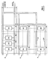
- FIG. 3 shows the conventional layout of an integrated circuit formed from a variety of standard cells 50.
- Cells 50 comprise one various configurations of components 52A, 52B, 52C, 52Z, etc. and are arranged in a matrix and interconnected by metallization (not shown) to form an integrated circuit.
- Cells 50 are of a standard height h and have power and ground connections routed across the top and bottom so that when cells 50 are arranged in rows 54 the power and ground connections abut to form power bus Vdd and ground bus Gnd which are then connected in common with the Vdd pin and ground pin to provide power to the circuit.
- Figure 4 shows incorporation of storage circuits as described above into the integrated circuit of Figure 3.
- Circuits 40 substantially as shown in Figure 2 (with appropriate component values) are connected between crypto power busses 44 (physically the same as busses Vdd) and the Vdd pin and busses Gnd at the end of each, or selected ones, of rows 54.
- a power control signal can be supplied either internally from the integrated circuit to power each row from circuits 40 during at least a substantial portion of the cryptographic operations performed by the circuit; or from an external device which knows when cryptographic operations are being performed.
- each storage circuit provides power to only a fraction of the integrated circuit the capacitors can be made very small and it is believed that individual circuits can be positioned at the end of each of rows 54 with minimal change to the layout of the integrated circuit while provision of a single storage circuit to power the whole integrated circuit would be very difficult or impossible within the constraints of the integrated circuit's geometry. In particular it should be noted that no change to the design or layout of the array of standard cells is needed.
- FIG. 5 shows another embodiment of the subject invention wherein only charging circuits 41 are positioned at the ends of rows 54, and each of cells 50 is slightly modified by the incorporation of capacitors 56 between bus 44 and bus Gnd for that row. Capacitors to power only a single cell are believed to be sufficiently small that they can be incorporated into an integrated circuit which would not have room for storage circuits sized to power a full row; though at the cost of redesign of the standard cells.
- FIG. 6 a graph is shown which is representative of the current drawn, as measured at line 30, by a portion of an RSA signature generation performed by cryptographic device 10 prior to implementation of the invention.
- the difference between squaring and multiply operations can be clearly seen.
- Multiply operations 62 require more power and therefore are represented by the higher peaks than squaring operations 60.
- the RSA key used can be easily derived from the graph of Figure 5.
- a 1 is represented by a square followed by a multiply (60-62 and 60"-62"), while a zero is represented by simply a square (60').
- FIG. 7 a graph is shown which illustrates the effectiveness of the present invention.
- the same portion of the RSA signature generation as shown in Figure 6 is depicted in Figure 7 after the addition of power storage circuit 40, in the form of an external circuit, to cryptographic device 10. It is noted that the peaks representative of the square and multiply operations previously observable in Figure 6 are no longer observable in Figure 7.
- the required storage capacity can be reduced still further by providing power from the storage circuits for only a fraction of the cryptographic operations.
- the cryptographic operations are divided into segments which are alternately powered from the storage circuits and the external power source.
- Figure 8 shows various embodiments of the subject invention wherein the cryptographic operations are variously segmented.
- Time line 70 shows cryptographic operations occurring between times T0 and T1, T2 and T3, etc. (Note that the cryptographic operations are shown as occurring regularly only for ease of illustration and generally will vary in both frequency and duration.)
- Time line 72 shows an embodiment of the subject invention wherein power is drawn from the storage circuits for the full duration of the cryptographic operations. This embodiment provides the maximum protection against DPA but requires the greatest capacity.
- Time line 74 shows an embodiment wherein alternately powered segments are distributed regularly over the cryptographic operations and in a fixed order over successive operations.
- Time line 76 shows an embodiment wherein alternately powered segments are distributed selectively over the cryptographic operations so that the most critical operations occur when power is taken from the storage circuits and in a fixed order over successive operations.
- Time line 76 shows an embodiment wherein alternately powered segments are distributed randomly over the cryptographic operations.
Description
- The present application shares common elements of disclosure with commonly assigned, co-pending
European application number: 99125306.3, filed December 17, 1999 EP-A-1 022 683 and titled: SYSTEM AND METHOD FOR SUPPRESSING CONDUCTED EMISSIONS BY A CRYPTOGRAPHIC DEVICE andEuropean application number 00 126 516.4 published as EP-A-1 107 502 , titled: SYSTEM AND METHOD FOR PREVENTING DIFFERENTIAL POWER ANALYSIS ATTACKS (DPA) ON A CRYPTOGRAPHIC DEVICE filed on even date herewith. - The subject invention relates generally to systems for carrying out cryptographic processes and, more particularly, to systems and methods for increasing the security of such systems; particularly such systems used to verify the payment of postage.
-
US-A-5,533,123 describes a method of limiting conducted emissions by a secured processing unit SPU performing encryption and decryption and various algorithms, the SPU comprising an SPU chip and performing at least a substantial portion of the cryptographic operations. The method comprises the steps of incorporating the SPU in a tamper-resistant structure, providing power to the SPU from an external battery and a system voltage line, and isolating at least a part of the SPU from the external battery when the system power is removed. -
EP-A-0 463 261 describes an IC card with improved power supply switching circuitry in which a voltage drop across a diode of the power supply switching circuit is kept small so that the IC card can always operate correctly. - Cryptographic systems have many applications both for the secure transmission of information and for the authentication and verification of the source of information. One such application is the verification of postage.
- The vast majority of the Posts around the world require prepayment for postal services provided by the Posts. Prepayment, however, requires verifiable evidence of paid postage. The traditional postage stamp is a prime example of such evidence.
- Another is the use of postage meters, which alleviate some shortcomings of postage stamps. The first postage meters were mechanical devices which securely coupled printing and accounting functions. The mechanical meter, which was perfected over the years, became a widespread basic business machine. The accounting and machine control functions were computerized when electronic postage meters were introduced in the late seventies. This enabled new features, including departmental accounting and computerized meter resetting. However, the fundamental security of postage evidencing remained the same; depending on two features: 1) physical security of the printing process, i.e., printing of postage evidence can not occur without appropriate accounting, and 2) forensic detectability, i.e., fraudulent postal indicia can be distinguished from legitimate indicia.
- Coupling the printing and accounting mechanism within a secure tamper-evident enclosure provides physical security of printing. Inspection of the device normally reveals tampering. Effective forensic detectability of fraudulent postal indicia depends on non-availability of alternative mechanisms suitable for forging indicia. Until recently, serious attempts to generate fraudulent indicia using an alternate printing mechanism were detectable.
- Today, the possible use of readily available, inexpensive computer-driven printers for printing postage evidence offer new opportunities for customer convenience and substantial cost advantages. However, the use of such printers requires new ways of verifying postage evidence, as was first suggested in U. S. Patents
4,641,347 ,4,641,346 ,4,757,537 , and4,775,246 . At that time, it was realized that the security of postage evidencing depends on the security of the information printed in the indicium, including message authentication and integrity. - U. S. Patents
4,831,555 and4,725,718 extended this idea to unsecured printing of postage; disclosing the necessity that at least some of the information in the indicium must appear random to a party not in possession of some secret. Such random looking information is commonly referred to as a digital token. - The basis of postal revenue security in the digital world is two new requirements: 1) security of the digital token generating process, i.e., digital tokens can not be generated without appropriate accounting, and 2) automatic detectability, i.e., fraudulent digital tokens can be detected by automatic means.
- A cryptographic transformation applied to selected data on the mailpiece produces the digital token. The data may include postage value, date, postal code of the geographical deposit area, recipient address information, meter data, and piece count. Such data is commonly referred to as postal data. The secret used to generate the digital token is generally a cryptographic key held within the accounting device. A verifier, with access to a verifying key corresponding to the accounting device secret, validates the digital token. Several cryptographic algorithms and protocols have been considered for this purpose. U. S. Patent
4,853,961 describes critical aspects of public-key cryptography for mailing applications. See José Pastor, CRYPTOPOST, A Universal Information-Based Franking System for Automated Mail Processing, Proceedings of the Fourth Advanced Technology Conference of the U. S. Postal Service, Vol. I, pp. 429-442, Nov. 1990. See also José Pastor, CRYPTOPOST, A Cryptographic Application to Mail Processing , Journal of Cryptology, 3 (2), pp. 137-146, Nov. 1990. - Two methods of presenting a postal verifier with fraudulent evidence of payment are a counterfeited indicium and a copied indicium. The former is an unpaid indicium that appears legitimate; in particular which will satisfy a cryptographic verification process. The latter is a replica of a legitimate paid indicium. Such counterfeit indicia will necessarily satisfy any cryptographic verification process and must be detected by other means; e.g. duplicate mailpiece numbers, etc., which form no part of the present invention. The present invention addresses the prevention of counterfeit indicium.
- A counterfeit indicium can be detected by verifying the digital token. Verification proves that the digital token was generated by a cryptographic algorithm with access to the secret meter key. The information printed in the indicium and access to a verifying key are sufficient for the detection of counterfeited indicia as long as the secret meter key is confidential. In a public-key system, a digital signature provides the data authentication and integrity check. In a symmetric-key system a message authentication code (MAC) provides a similar check.
- Assuming integrity of the verification software and hardware, only a compromised meter secret-key can produce verifiable counterfeit indicia. Meters can be compromised by violating the physical protection of the key by tampering, or by deriving the key from indicia data by cryptanalysis. Generally, tampering is detectable if the physical protection of the secure component of the postage metering system is adequate, for example as set forth in FIPS 140-1, Security Requirements for Cryptographic Modules, National Institute for Standards and Technology, Jan. 1994, and protection against physical tampering forms no part of the subject invention.
- In general various cryptographic operations for generating digital tokens to authenticate postal indicia and to verify such indicia are well known and details of various systems need not be discussed further here for an understanding of the subject invention except to note that robustness of all such operations against cryptanalysis depends on the difficulty of solving certain mathematical problems, for example, discrete logarithm problems or factoring a large composite number. (see: The USPS published draft specifications: The INFORMATION BASED INDICIA PROGRAM (IBIP) INDICIUM SPECIFICATION, dated June 13, 1996; The INFORMATION BASED INDICIA PROGRAM POSTAL SECURITY DEVICE SPECIFICATION, dated June 13, 1996; and The INFORMATION BASED INDICIA PROGRAM HOST SYSTEM SPECIFICATION, dated October 9, 1996, which together define the U.S.P.S.'s proposed requirements for a postage payment system based upon cryptographically secured indicia.)
- As part of its proposed Information-Based Indicia Program (IBIP), the USPS has proposed 1024 bit RSA, 1024 bit DSS or 160 bit ECDSA as measures of robustness.
- Presently, there are two postage metering types: closed systems and open systems. In a closed system, the system functionality is solely dedicated to metering activity. An open system metering device is a postage evidencing device with a non-dedicated printer; i.e. one that is not securely coupled to a secure accounting module and can be used for other purposes. Open system indicia printed by the non-dedicated printer are made secure by including addressee information in the encrypted evidence of postage printed on the mailpiece for subsequent verification. Examples of open system metering devices include personal computer (PC) based devices with single/multi-tasking operating systems, multi-user applications and digital printers.
- Conventional closed system mechanical and electronic postage meters have heretofore secured the link between printing and accounting. The integrity of the physical meter box has been monitored by periodic inspections of the meters. Digital printing postage meters, which are closed system postage meters, typically include a digital printer coupled to a metering (accounting) device, which is referred to herein as a postal security device (PSD). Digital printing postage meters have removed the need for physical inspection by cryptographically securing the link between the accounting and printing mechanisms. In essence, new digital printing postage meters create a secure point to point communication link between the accounting unit and printhead. See, for example,
U.S. Patent No. 4,802,218, issued to Christopher B. Wright et al and now assigned to the assignee of the present invention. - An example of a digital printing postage meter with secure printhead communication is the Personal Post™ manufactured by Pitney Bowes Inc. of Stamford, CT. An example of a digital printing postage meter in a secure housing is the PostPerfect™ also manufactured by Pitney Bowes Inc. Either type of digitally printing system can use cryptographically secured digital tokens.
- As noted above the security of cryptographically secured postage metering systems, as well as other cryptographic information systems, is based on an assumption that the secret information, i.e., the crypto keys, stored within a secure cryptographic device are protected against disclosure to any attacker. With physical security in effect, it has been assumed that an attacker could only obtain crypto keys either by trying all the possible crypto keys associated with the algorithm being used (symmetric algorithms) or by carrying out a complex mathematical search (asymmetric algorithms). For accepted cryptographic algorithms, this search is prohibitive, e.g. obtaining a 1024 bit RSA key requires 230 years of 300 Mhz PC computing.
- A recently published technique, Differential Power Analysis (DPA), undermines this assumption and seriously threatens the security of cryptographic devices. The technique involves observation and analysis of fluctuations on the power line of a cryptographic device (hereinafter sometimes "conducted emissions") to determine the cryptographic secrets, i.e., the crypto keys, used by the device. DPA attack allows one to extract secret protected information from a supposedly secure cryptographic device by measuring variations in power consumption over time, and then applying sophisticated analysis to this information. As the cryptographic processor performs its cryptographic functions, such as encryption or signing; transistors comprising the processor switch on and off, which changes the amount of current drawn from the source supplying power to the processor. Assuming the attacker has some knowledge of the functions performed by the cryptographic processor, the attacker can correlate the current changes with data being processed and the crypto keys being used. Any type of secure cryptographic device that obtains its operating power from an external source is potentially susceptible to the attack. Such devices include smart cards, PC (PCMCIA) cards and printed circuit boards, including devices that are housed within a protected enclosure. If such a cryptographic device is subjected to DPA attack, then the crypto key can be obtained in a matter of days or weeks. Many of the proposed countermeasures to the DPA attack involve the introduction of signal noise or filters on the power line, random timing and delays during cryptographic processing, and the introduction of extraneous operations. These countermeasures make the attack much more difficult. However, an attacker can overcome them by obtaining more samples of power line fluctuations and applying more sophisticated analytical techniques.
- While it is important that the security community at large find means either to defeat this attack, or to at least greatly lengthen the time and expertise needed to successfully carry it out, it is believed particularly important for the successful adoption of cryptographically secured postage metering systems. In many, if not most other cryptographic systems, cryptographic devices and their associated keys are in the custody of the "owner" who, in principle, has incentive to protect them. Postage metering systems however are not used in the custody of either party most concerned with system integrity, the system vendor or the Post, but by a mailer; who, if dishonest, has every reason to try to defeat the system. To further complicate the problem, a desired advantage of digital postage metering systems is the reduced need for physical inspections; further opening the window of opportunity for the dishonest mailer. And the large number of systems in use will greatly increase the chances that some will fall into the hands of the dishonest; and even a single meter which is compromised can be used to generate substantial amounts of fraudulent indicia since a successfully counterfeited indicium will not be readily detected by the methods used to detect simple duplicate indicia. Additionally postage metering systems can send thousands of encrypted messages, i.e. postal indicia, a day; greatly simplifying the sampling task of the DPA attacker. And all these problems must be overcome without adding substantially to postage costs.
- Similar considerations also apply to other types of value metering systems, which are systems which similarly account for and evidence the delivery, receipt, or payment for other forms of value (e.g. tax stamp meters) by generating indicia or other types of messages, which may be secured cryptographically.
- Thus it is an object of the subject invention to provide cryptographic devices, and particularly cryptographically secured postage metering systems, with protection against DPA attack.
- According to one aspect of the invention, there is provided a method of limiting conducted emissions by a cryptographic device performing cryptographic operations, said cryptographic device comprising an integrated circuit having a secure housing, said integrated circuit including a row of cells and performing at least a portion of said cryptographic operations, the method comprising the steps of: providing power to said integrated circuit from a first power source, said first power source being external to the secure housing; locating a power storage circuit within said secure housing for said integrated circuit, said power storage circuit including a second power source and a charging circuit, said charging circuit being located at one end of said row of cells of said integrated circuit; isolating at least a part of said integrated circuit including said row of cells from said first power source during at least a part of said portion of said cryptographic operations; and providing power to said at least a part of said integrated circuit including said row of cells from the second power source at least part of the time when said integrated circuit is performing said at least a part of said portion of said cryptographic operations.
- In accordance with one embodiment, providing power to the integrated circuit includes: switching at least the part of the integrated circuit including said row of cells from the first power source to the second power source prior to or during the substantial portion of the cryptographic operations; and switching at least the part of the integrated circuit including said row of cells from the second power source to the first power source subsequent to or during the portion of the cryptographic operations.
- In accordance with another variant, the second power source stores power from the first power source and provides power to at least a part of the integrated circuit including the row of cells during said at least part of the time when at least a part of the cryptographic operations are being performed by said integrated circuit.
- In accordance with another variant, the cryptographic operations are divided into a plurality of segments and the second power source stores power from the first power source between alternate ones of the segments.
- In accordance with another variant, said second power source includes a plurality of capacitors, each being located proximate to a corresponding one of the cells.
- In accordance with another variant, the invention is applicable to other types of value metering systems where cryptographically secured indicia are used as evidence of value received, delivered or purchased.
- In one variant the cryptographic operations generate a digital token for a postal indicium.
- According to another aspect of the invention, there is provided a cryptographic system for performing cryptographic operations, comprising: an integrated circuit having a secure housing, said integrated circuit including a row of cells that form a part of a processor for performing cryptographic operations; a first power source coupled to and supplying power to said processor, said first power source being external to said secure housing of said integrated circuit; a power storage circuit within the secure housing of said integrated circuit coupled to and supplying power to at least said part of said processor formed by said rows of cells, said power storage circuit including a second power source and a charging circuit, said charging circuit being physically located at one end of said rows of cells; and said power storage circuit being responsive to a power control signal from said processor for switching between said first power source and said second power source, said power storage circuit being operable to isolate said at least a part of said processor formed by said row of cells from said first power source so that said second power source is operable to provide power to said at least a part of said processor formed by said row of cells when said processor is performing at least a portion of said cryptographic operations.
- Other objects and advantages of the subject invention will be apparent to those skilled in the art from consideration of the attached drawings and the detailed description set forth below. In the drawings:
- Fig. 1 is a block diagram of a traditional cryptographic device (prior art);
- Fig. 2 is a temporary power storage circuit for use with the device of Fig. 1 in accordance with an embodiment of the present invention;
- Fig. 3 is a semi-schematic block diagram of a conventional layout of an integrated circuit comprising an array of standard cells;
- Fig. 4 is a semi-schematic block diagram of an integrated circuit having a storage circuit in accordance with an embodiment of the subject invention;
- Fig. 5 is a semi-schematic block diagram of an integrated circuit having a storage circuit in accordance with an alternative embodiment of the subject invention;
- Fig. 6 is a graph which is representative of the current drawn by a portion of an RSA signature generation performed by the device of Fig. 1 prior to implementation of the present invention;
- Fig. 7 a graph which is representative of the current drawn by a portion of an RSA signature generation performed by the device of Fig. 1 after implementation of the present invention; and
- Figure 8 is a timing diagram of alternative embodiments of the subject invention.
- Referring now to Fig. 1, a block diagram of a traditional cryptographic device, generally designated 10, is shown.
Cryptographic device 10 includes aconventional processor 20, coupled to anoptional cryptographic coprocessor 22 for performing cryptographic operations,non-volatile memory 24,random access memory 26 and read-only memory 28.Cryptographic device 10 is enclosed within asecure housing 34. Thesecure housing 34 may be any conventional means for preventing access tocryptographic device 10. For example,secure housing 34 may be an integrated circuit chip encased in an epoxy or ceramic housing that prevents access to the integrated circuit without destruction of the integrated circuit. Power tocryptographic device 10 is input atpower line 30. Input/output communications occur at I/O line 32. It will be understood thatcryptographic device 10 may be implemented as any number of discrete components or as a single integrated circuit, such as a smart card. - In a preferred embodiment,
device 10 can comprise a postage metering system whereprocessor 20 is controlled by program code stored in read-only memory 28, to carry out the functions of a postage metering system such as accounting for postage innon-volatile memory 24 and controlling a printer (not shown) to print a postal indicium including a digital token formed by encryption of postal information byco-processor 22. Details of the construction, programming and operation of such postage metering systems are known and need not be discussed further here for an understanding of the subject invention except to note that, as discussed above, the protection of the crypto-keys used from side-channel attacks such as DPA is both critical to the security of such postage metering systems and difficult to achieve within the constraints of such systems. - In other embodiments of the
subject invention device 10 can comprise other types of value metering systems. - Referring now to Fig. 2, a power storage circuit, generally designated 40, is shown that can be used with
cryptographic device 10 in accordance with the present invention.Power storage circuit 40, which is connected topower line 30 atline 36, includes a capacitor C1, and a chargingcircuit 41 made up of transistor Q1, and three resistors R1, R2 and R3. By placingpower storage circuit 40 between the externalpower input line 30 andcrypto coprocessor 22 transistor Q1 acts as a switch under control ofpower control line 42, so thatcircuit 40 controls whether power is supplied by the external power input atpower line 30 or capacitor C1. - When processor 20 (or
co-processor 22, depending upon the details of the programming) determines that cryptographic operations are not being performed, the power control line, generally designated 42, is used to closeswitch 41, i.e. transistor Q1, allowing capacitor C1 to accumulate charge. During cryptographic operations,processor 20 opens switch 41 and the charge stored in capacitor C1 is used to powercryptographic coprocessor 22 through the crypto power line, generally designated 44. Whenswitch 41 is open, no power fluctuations ofcryptographic coprocessor 22 are conducted out the externalpower input line 30 and, therefore, fluctuations online 30 cannot be correlated with individual cryptographic operations, and DPA cannot be performed. - Particular values for components of
circuit 40 in particular applications will depend upon the power drawn by the load ofco-processor 22, the time for which power is to be drawn from capacitor C1, the minimum voltage required for operation, and the energy available for recharge. Selection of these values for particular applications is well within the abilities of a person skilled in the art. - In some implementations, a storage device large enough to supply power for the entire cryptographic operation cannot be implemented. For example, when
cryptographic device 10 is a single integrated circuit andpower storage circuit 40 is part of the integrated circuit, a large enough capacitor C1 to supply power for the entire cryptographic operation may not be available. In such implementations, a smaller storage device can be used to supply power for part of the cryptographic operation. The cryptographic processing can be halted while the storage device recharges and resumed after the storage device has been sufficiently charged. Alternatively, processing can continue while the storage device recharges. However, in either case information concerning the cryptographic key used in the cryptographic operation will be conducted out the externalpower input line 30 although not to the same degree as without the circuit in place. If either of these techniques is used in conjunction with the proposed countermeasures discussed previously (the introduction of signal noise or filters on the power line, random timing and delays during cryptographic processing, and the introduction of extraneous operations) a high level of DPA resistance can be achieved. - It is immediately apparent from inspection of Figure 2 that
circuit 40 must be withinhousing 34 and that security against DPA attacks depends upon the integrity ofhousing 34. If an attacker can penetratehousing 34 DPA can be conducted online 44 whether or not co-processor 22 is powered fromexternal power line 36. For this reason embodiments of the subject invention wheredevice 10, or at least that part of the device which performs cryptographic operations,e.g. co-processor 22, is comprised in an integrated circuit which also includescircuit 40 are desirable. Without great difficulty the hermetically sealed housing of an integrated circuit cannot be penetrated without making the circuit inoperative. Thus it is believed that the conventional housing of an integrated circuit will provide a highly effective embodiment of, or supplement for,housing 34 without substantial increase in the cost of the integrated circuit. As discussed above this will be particularly advantageous in postage metering systems. - Unfortunately, storage devices with sufficient capacity to power a substantial portion of the cryptographic operations are, with present technology, too large to implement on an integrated circuit. This difficulty is overcome in accordance with the subject invention by taking advantage of the conventional design of integrated circuits.
- Figure 3 shows the conventional layout of an integrated circuit formed from a variety of
standard cells 50.Cells 50 comprise one various configurations ofcomponents Cells 50 are of a standard height h and have power and ground connections routed across the top and bottom so that whencells 50 are arranged inrows 54 the power and ground connections abut to form power bus Vdd and ground bus Gnd which are then connected in common with the Vdd pin and ground pin to provide power to the circuit. - Figure 4 shows incorporation of storage circuits as described above into the integrated circuit of Figure 3.
Circuits 40, substantially as shown in Figure 2 (with appropriate component values) are connected between crypto power busses 44 (physically the same as busses Vdd) and the Vdd pin and busses Gnd at the end of each, or selected ones, ofrows 54. A power control signal can be supplied either internally from the integrated circuit to power each row fromcircuits 40 during at least a substantial portion of the cryptographic operations performed by the circuit; or from an external device which knows when cryptographic operations are being performed. - Since each storage circuit provides power to only a fraction of the integrated circuit the capacitors can be made very small and it is believed that individual circuits can be positioned at the end of each of
rows 54 with minimal change to the layout of the integrated circuit while provision of a single storage circuit to power the whole integrated circuit would be very difficult or impossible within the constraints of the integrated circuit's geometry. In particular it should be noted that no change to the design or layout of the array of standard cells is needed. - Figure 5 shows another embodiment of the subject invention wherein only charging
circuits 41 are positioned at the ends ofrows 54, and each ofcells 50 is slightly modified by the incorporation ofcapacitors 56 betweenbus 44 and bus Gnd for that row. Capacitors to power only a single cell are believed to be sufficiently small that they can be incorporated into an integrated circuit which would not have room for storage circuits sized to power a full row; though at the cost of redesign of the standard cells. - Referring now to Figure 6, a graph is shown which is representative of the current drawn, as measured at
line 30, by a portion of an RSA signature generation performed bycryptographic device 10 prior to implementation of the invention. The difference between squaring and multiply operations can be clearly seen. Multiplyoperations 62 require more power and therefore are represented by the higher peaks than squaringoperations 60. The RSA key used can be easily derived from the graph of Figure 5. A 1 is represented by a square followed by a multiply (60-62 and 60"-62"), while a zero is represented by simply a square (60'). - Referring now to Figure 7, a graph is shown which illustrates the effectiveness of the present invention. The same portion of the RSA signature generation as shown in Figure 6 is depicted in Figure 7 after the addition of
power storage circuit 40, in the form of an external circuit, tocryptographic device 10. It is noted that the peaks representative of the square and multiply operations previously observable in Figure 6 are no longer observable in Figure 7. - A discussed above, the required storage capacity can be reduced still further by providing power from the storage circuits for only a fraction of the cryptographic operations. The cryptographic operations are divided into segments which are alternately powered from the storage circuits and the external power source. Figure 8 shows various embodiments of the subject invention wherein the cryptographic operations are variously segmented.
-
Time line 70 shows cryptographic operations occurring between times T0 and T1, T2 and T3, etc. (Note that the cryptographic operations are shown as occurring regularly only for ease of illustration and generally will vary in both frequency and duration.)Time line 72 shows an embodiment of the subject invention wherein power is drawn from the storage circuits for the full duration of the cryptographic operations. This embodiment provides the maximum protection against DPA but requires the greatest capacity.Time line 74 shows an embodiment wherein alternately powered segments are distributed regularly over the cryptographic operations and in a fixed order over successive operations.Time line 76 shows an embodiment wherein alternately powered segments are distributed selectively over the cryptographic operations so that the most critical operations occur when power is taken from the storage circuits and in a fixed order over successive operations.Time line 76 shows an embodiment wherein alternately powered segments are distributed randomly over the cryptographic operations. - It is believed that a fixed order of segmentation will provide the greatest degree of protection against advanced DPA attacks.
Claims (19)
- A method of limiting conducted emissions by a cryptographic device performing cryptographic operations, said cryptographic device comprising an integrated circuit (10) having a secure housing (34), said integrated circuit including a row of cells (50) and performing at least a portion of said cryptographic operations, the method comprising the steps of:providing power to said integrated circuit (10) from a first power source (30), said first power source being external to the secure housing (34);locating a power storage circuit (40) within said secure housing for said integrated circuit, said power storage circuit including a second power source (C1; 56) and a charging circuit (41), said charging circuit (41) being located at one end of said row of cells (50) of said integrated circuit;isolating at least a part of said integrated circuit (10) including said row of cells (50) from said first power source (30) during at least a part of said portion of said cryptographic operations; andproviding power to said at least a part (22) of said integrated circuit (10) including said row of cells (50) from the second power source (C1; 56) at least part of the time when said integrated circuit is performing said at least a part of said portion of said cryptographic operations.
- The method of Claim 1, wherein the steps of providing power includes the steps of:switching at least said part of said integrated circuit (10) including said row of cells (50) from said first power source (30) to said second power source (C1; 56) prior to or during said portion of said cryptographic operations; andswitching at least said part (22) of said integrated circuit (10) including said row of cells (50) from the second power source (C1; 56) to the first power source (30) subsequent to or during said portion of said cryptographic operations.
- The method of Claim 1, wherein said second power source (C1; 56) stores power from said first power source (30) and provides power to said at least a part of said integrated circuit including said row of cells (50) during said at least part of the time when said integrated circuit is performing said at least a part of said portion of said cryptographic operations.
- The method of Claim 3, wherein said cryptographic operations are divided into a plurality of segments and wherein said second power source (C1; 56) stores power from the first power source (30) between alternate ones of said segments.
- The method of Claim 4, wherein said segments are distributed over said cryptographic operations in a fixed order.
- The method of Claim 4, wherein said segments are distributed over said cryptographic operations in a random order.
- The method of any one of Claims 1 to 6, wherein said second power source includes a capacitor (C1), said capacitor (C1) being located at one end of said row of cells (50) of said integrated circuit along with said charging circuit (41).
- The method of any one of Claims 1 to 6, wherein said second power source includes a plurality of capacitors (56), each of the plurality of capacitors being located proximate to a corresponding one of said cells (50).
- The method of any one of Claims 1 to 8, wherein said cryptographic operations generate a digital token for a postal indicium.
- The method of any one of Claims 1 to 8, wherein said cryptographic operations generate a secure message for a value metering system.
- A cryptographic system for performing cryptographic operations, comprising:an integrated circuit (10) having a secure housing (34), said integrated circuit including a row of cells (50) that form a part of a processor (20,22) for performing cryptographic operations;a first power source (30) coupled to and supplying power to said processor, said first power source being external to said secure housing (34) of said integrated circuit;a power storage circuit (40) within the secure housing (34) of said integrated circuit coupled to and supplying power to at least said part of said processor formed by said rows of cells (50), said power storage circuit (40) including a second power source (C1; 56) and a charging circuit (41), said charging circuit (41) being physically located at one end of said rows of cells (50); andsaid power storage circuit (40) being responsive to a power control signal from said processor for switching between said first power source (30) and said second power source (C1; 56), said power storage circuit being operable to isolate said at least a part of said processor formed by said row of cells (50) from said first power source (30) so that said second power source is operable to provide power to said at least a part of said processor formed by said row of cells (50) when said processor is performing at least a portion of said cryptographic operations.
- The system of Claim 11, wherein said second power source includes a capacitor (C1; 56), said capacitor being charged at least part of the time and discharged to supply power to said at least a part of said processor formed by said row of cells at least part of the time when said cryptographic operations are being performed.
- The system of Claim 12, wherein said cryptographic operations are divided into a plurality of segments and wherein said second power source is recharged between alternate ones of said segments.
- The system of Claim 13, wherein said segments are distributed over said cryptographic operations in a fixed order.
- The system of Claim 13, wherein said segments are distributed over said cryptographic operations in a random order.
- The system of any one of Claims 11 to 15, wherein said second power source includes a plurality of capacitors (56) and a respective capacitor is located proximate to each of said cells in said row.
- The system of any one of Claims 11 to 15, wherein said second power source includes a capacitor (C1), said capacitor being located at one end of said row of cells (50) of said integrated circuit along with said charging circuit (41).
- The system of any one of Claims 11 to 17, wherein said cryptographic operations generate a digital token for a postal indicium.
- The system of any one of Claims 11 to 17, wherein said cryptographic operations generate a secure message for a value metering system.
Applications Claiming Priority (2)
| Application Number | Priority Date | Filing Date | Title |
|---|---|---|---|
| US458638 | 1999-12-09 | ||
| US09/458,638 US6748535B1 (en) | 1998-12-21 | 1999-12-09 | System and method for suppressing conducted emissions by a cryptographic device comprising an integrated circuit |
Publications (2)
| Publication Number | Publication Date |
|---|---|
| EP1107191A1 EP1107191A1 (en) | 2001-06-13 |
| EP1107191B1 true EP1107191B1 (en) | 2007-06-27 |
Family
ID=23821545
Family Applications (1)
| Application Number | Title | Priority Date | Filing Date |
|---|---|---|---|
| EP00126515A Expired - Lifetime EP1107191B1 (en) | 1999-12-09 | 2000-12-08 | System and method for suppressing conducted emissions by a cryptographic device comprising an integrated circuit |
Country Status (3)
| Country | Link |
|---|---|
| EP (1) | EP1107191B1 (en) |
| CA (1) | CA2327943C (en) |
| DE (1) | DE60035331T2 (en) |
Families Citing this family (4)
| Publication number | Priority date | Publication date | Assignee | Title |
|---|---|---|---|---|
| US8912816B2 (en) | 2012-11-12 | 2014-12-16 | Chaologix, Inc. | Charge distribution control for secure systems |
| US8912814B2 (en) | 2012-11-12 | 2014-12-16 | Chaologix, Inc. | Clocked charge domain logic |
| US9069959B2 (en) | 2012-12-21 | 2015-06-30 | Nxp B.V. | Cryptographic circuit protection from differential power analysis |
| CN105431861A (en) * | 2013-05-31 | 2016-03-23 | 科欧罗基克斯有限公司 | Charge distribution control for secure systems |
Citations (1)
| Publication number | Priority date | Publication date | Assignee | Title |
|---|---|---|---|---|
| US5533123A (en) * | 1994-06-28 | 1996-07-02 | National Semiconductor Corporation | Programmable distributed personal security |
Family Cites Families (15)
| Publication number | Priority date | Publication date | Assignee | Title |
|---|---|---|---|---|
| US4641347A (en) | 1983-07-18 | 1987-02-03 | Pitney Bowes Inc. | System for printing encrypted messages with a character generator and bar-code representation |
| US4641346A (en) | 1983-07-21 | 1987-02-03 | Pitney Bowes Inc. | System for the printing and reading of encrypted messages |
| US4725718A (en) | 1985-08-06 | 1988-02-16 | Pitney Bowes Inc. | Postage and mailing information applying system |
| US4775246A (en) | 1985-04-17 | 1988-10-04 | Pitney Bowes Inc. | System for detecting unaccounted for printing in a value printing system |
| US4831555A (en) | 1985-08-06 | 1989-05-16 | Pitney Bowes Inc. | Unsecured postage applying system |
| US4757537A (en) | 1985-04-17 | 1988-07-12 | Pitney Bowes Inc. | System for detecting unaccounted for printing in a value printing system |
| US4853961A (en) | 1987-12-18 | 1989-08-01 | Pitney Bowes Inc. | Reliable document authentication system |
| FR2638869B1 (en) * | 1988-11-10 | 1990-12-21 | Sgs Thomson Microelectronics | SECURITY DEVICE AGAINST UNAUTHORIZED DETECTION OF PROTECTED DATA |
| JPH0449485A (en) * | 1990-06-19 | 1992-02-18 | Mitsubishi Electric Corp | Ic card |
| DE19505097C1 (en) * | 1995-02-15 | 1996-06-05 | Siemens Ag | Encryption device |
| GB9811637D0 (en) * | 1998-05-29 | 1998-07-29 | Madge Networks Ltd | A power supply interface |
| DE19850293A1 (en) * | 1998-10-30 | 2000-05-04 | Koninkl Philips Electronics Nv | Media with protection against compromise |
| US6594760B1 (en) | 1998-12-21 | 2003-07-15 | Pitney Bowes Inc. | System and method for suppressing conducted emissions by a cryptographic device |
| DE19911673A1 (en) * | 1999-03-09 | 2000-09-14 | Deutsche Telekom Ag | Method and arrangement for protecting data on a smart card |
| FR2793904B1 (en) * | 1999-05-21 | 2001-07-27 | St Microelectronics Sa | METHOD AND DEVICE FOR MANAGING AN ELECTRONIC CIRCUIT |
-
2000
- 2000-12-08 DE DE60035331T patent/DE60035331T2/en not_active Expired - Lifetime
- 2000-12-08 CA CA002327943A patent/CA2327943C/en not_active Expired - Fee Related
- 2000-12-08 EP EP00126515A patent/EP1107191B1/en not_active Expired - Lifetime
Patent Citations (1)
| Publication number | Priority date | Publication date | Assignee | Title |
|---|---|---|---|---|
| US5533123A (en) * | 1994-06-28 | 1996-07-02 | National Semiconductor Corporation | Programmable distributed personal security |
Also Published As
| Publication number | Publication date |
|---|---|
| CA2327943A1 (en) | 2001-06-09 |
| DE60035331T2 (en) | 2008-02-28 |
| EP1107191A1 (en) | 2001-06-13 |
| CA2327943C (en) | 2005-09-20 |
| DE60035331D1 (en) | 2007-08-09 |
Similar Documents
| Publication | Publication Date | Title |
|---|---|---|
| US6748535B1 (en) | System and method for suppressing conducted emissions by a cryptographic device comprising an integrated circuit | |
| US6766455B1 (en) | System and method for preventing differential power analysis attacks (DPA) on a cryptographic device | |
| US6724894B1 (en) | Cryptographic device having reduced vulnerability to side-channel attack and method of operating same | |
| EP0931299B1 (en) | Virtual postage meter with secure digital signature device | |
| US6795813B2 (en) | System and method for linking an indicium with address information of a mailpiece in a closed system postage meter | |
| EP1469426A2 (en) | Postage meter device and system and method for communications with postage meters | |
| US6986057B1 (en) | Security device and method | |
| EP0899696B1 (en) | Method and system for enhancing security and for audit and control of cryptographic verifier | |
| EP1107191B1 (en) | System and method for suppressing conducted emissions by a cryptographic device comprising an integrated circuit | |
| AU2002226272B2 (en) | Method for providing letters and parcels with postal remarks | |
| US20050268099A1 (en) | Security device and method | |
| EP1107506B1 (en) | Method and system for generating messages including a verifiable assertion that a variable is within predetermined limits | |
| US8255334B2 (en) | Method for providing postal items with postal prepayment impressions | |
| US6938023B1 (en) | Method of limiting key usage in a postage metering system that produces cryptographically secured indicium | |
| US20080109359A1 (en) | Value Transfer Center System | |
| VAISSIERE et al. | Security Policy N30i/N30ig-135/136 Meter | |
| MXPA99001576A (en) | Virtual postage meter with secure digital signature device |
Legal Events
| Date | Code | Title | Description |
|---|---|---|---|
| PUAI | Public reference made under article 153(3) epc to a published international application that has entered the european phase |
Free format text: ORIGINAL CODE: 0009012 |
|
| AK | Designated contracting states |
Kind code of ref document: A1 Designated state(s): DE FR GB |
|
| AX | Request for extension of the european patent |
Free format text: AL;LT;LV;MK;RO;SI |
|
| 17P | Request for examination filed |
Effective date: 20011212 |
|
| AKX | Designation fees paid |
Free format text: DE FR GB |
|
| 17Q | First examination report despatched |
Effective date: 20050527 |
|
| 17Q | First examination report despatched |
Effective date: 20050527 |
|
| GRAP | Despatch of communication of intention to grant a patent |
Free format text: ORIGINAL CODE: EPIDOSNIGR1 |
|
| RIC1 | Information provided on ipc code assigned before grant |
Ipc: H04K 3/00 20060101ALI20070215BHEP Ipc: G07B 17/00 20060101AFI20070215BHEP Ipc: G06F 21/00 20060101ALI20070215BHEP |
|
| GRAS | Grant fee paid |
Free format text: ORIGINAL CODE: EPIDOSNIGR3 |
|
| GRAA | (expected) grant |
Free format text: ORIGINAL CODE: 0009210 |
|
| AK | Designated contracting states |
Kind code of ref document: B1 Designated state(s): DE FR GB |
|
| REG | Reference to a national code |
Ref country code: GB Ref legal event code: FG4D |
|
| REF | Corresponds to: |
Ref document number: 60035331 Country of ref document: DE Date of ref document: 20070809 Kind code of ref document: P |
|
| ET | Fr: translation filed | ||
| PLBE | No opposition filed within time limit |
Free format text: ORIGINAL CODE: 0009261 |
|
| STAA | Information on the status of an ep patent application or granted ep patent |
Free format text: STATUS: NO OPPOSITION FILED WITHIN TIME LIMIT |
|
| 26N | No opposition filed |
Effective date: 20080328 |
|
| REG | Reference to a national code |
Ref country code: FR Ref legal event code: PLFP Year of fee payment: 16 |
|
| REG | Reference to a national code |
Ref country code: FR Ref legal event code: PLFP Year of fee payment: 17 |
|
| PGFP | Annual fee paid to national office [announced via postgrant information from national office to epo] |
Ref country code: GB Payment date: 20161228 Year of fee payment: 17 |
|
| PGFP | Annual fee paid to national office [announced via postgrant information from national office to epo] |
Ref country code: FR Payment date: 20161227 Year of fee payment: 17 |
|
| PGFP | Annual fee paid to national office [announced via postgrant information from national office to epo] |
Ref country code: DE Payment date: 20161229 Year of fee payment: 17 |
|
| REG | Reference to a national code |
Ref country code: DE Ref legal event code: R119 Ref document number: 60035331 Country of ref document: DE |
|
| GBPC | Gb: european patent ceased through non-payment of renewal fee |
Effective date: 20171208 |
|
| REG | Reference to a national code |
Ref country code: FR Ref legal event code: ST Effective date: 20180831 |
|
| PG25 | Lapsed in a contracting state [announced via postgrant information from national office to epo] |
Ref country code: DE Free format text: LAPSE BECAUSE OF NON-PAYMENT OF DUE FEES Effective date: 20180703 Ref country code: FR Free format text: LAPSE BECAUSE OF NON-PAYMENT OF DUE FEES Effective date: 20180102 |
|
| PG25 | Lapsed in a contracting state [announced via postgrant information from national office to epo] |
Ref country code: GB Free format text: LAPSE BECAUSE OF NON-PAYMENT OF DUE FEES Effective date: 20171208 |