EP1113530B1 - High speed card edge connectors - Google Patents
High speed card edge connectors Download PDFInfo
- Publication number
- EP1113530B1 EP1113530B1 EP00128102A EP00128102A EP1113530B1 EP 1113530 B1 EP1113530 B1 EP 1113530B1 EP 00128102 A EP00128102 A EP 00128102A EP 00128102 A EP00128102 A EP 00128102A EP 1113530 B1 EP1113530 B1 EP 1113530B1
- Authority
- EP
- European Patent Office
- Prior art keywords
- ground
- contact
- contacts
- engagement
- elongated
- Prior art date
- Legal status (The legal status is an assumption and is not a legal conclusion. Google has not performed a legal analysis and makes no representation as to the accuracy of the status listed.)
- Expired - Lifetime
Links
Images


Classifications
-
- H—ELECTRICITY
- H01—ELECTRIC ELEMENTS
- H01R—ELECTRICALLY-CONDUCTIVE CONNECTIONS; STRUCTURAL ASSOCIATIONS OF A PLURALITY OF MUTUALLY-INSULATED ELECTRICAL CONNECTING ELEMENTS; COUPLING DEVICES; CURRENT COLLECTORS
- H01R13/00—Details of coupling devices of the kinds covered by groups H01R12/70 or H01R24/00 - H01R33/00
- H01R13/64—Means for preventing incorrect coupling
-
- H—ELECTRICITY
- H01—ELECTRIC ELEMENTS
- H01R—ELECTRICALLY-CONDUCTIVE CONNECTIONS; STRUCTURAL ASSOCIATIONS OF A PLURALITY OF MUTUALLY-INSULATED ELECTRICAL CONNECTING ELEMENTS; COUPLING DEVICES; CURRENT COLLECTORS
- H01R12/00—Structural associations of a plurality of mutually-insulated electrical connecting elements, specially adapted for printed circuits, e.g. printed circuit boards [PCB], flat or ribbon cables, or like generally planar structures, e.g. terminal strips, terminal blocks; Coupling devices specially adapted for printed circuits, flat or ribbon cables, or like generally planar structures; Terminals specially adapted for contact with, or insertion into, printed circuits, flat or ribbon cables, or like generally planar structures
- H01R12/70—Coupling devices
- H01R12/71—Coupling devices for rigid printing circuits or like structures
- H01R12/712—Coupling devices for rigid printing circuits or like structures co-operating with the surface of the printed circuit or with a coupling device exclusively provided on the surface of the printed circuit
- H01R12/714—Coupling devices for rigid printing circuits or like structures co-operating with the surface of the printed circuit or with a coupling device exclusively provided on the surface of the printed circuit with contacts abutting directly the printed circuit; Button contacts therefore provided on the printed circuit
-
- H—ELECTRICITY
- H01—ELECTRIC ELEMENTS
- H01R—ELECTRICALLY-CONDUCTIVE CONNECTIONS; STRUCTURAL ASSOCIATIONS OF A PLURALITY OF MUTUALLY-INSULATED ELECTRICAL CONNECTING ELEMENTS; COUPLING DEVICES; CURRENT COLLECTORS
- H01R12/00—Structural associations of a plurality of mutually-insulated electrical connecting elements, specially adapted for printed circuits, e.g. printed circuit boards [PCB], flat or ribbon cables, or like generally planar structures, e.g. terminal strips, terminal blocks; Coupling devices specially adapted for printed circuits, flat or ribbon cables, or like generally planar structures; Terminals specially adapted for contact with, or insertion into, printed circuits, flat or ribbon cables, or like generally planar structures
- H01R12/70—Coupling devices
- H01R12/7005—Guiding, mounting, polarizing or locking means; Extractors
- H01R12/7011—Locking or fixing a connector to a PCB
- H01R12/7017—Snap means
Abstract
Description
Claims (19)
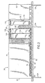
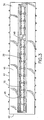
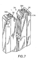
- A module (40, 40A) for use with a modular card edge electrical connector comprising:wherein the first elongated contact (62) includes a second contact surface (72) projecting into the card receiving recess (60) for engagement with a first conductive contact member (34) on the planar card (28, 28A) inserted into the card receiving recess (60) and the second elongated contact (66) includes a second contact surface (74) projecting into the card receiving recess (60) in the direction of the first elongated contact (62) for engagement with a second conductive contact member (34) on the planar card (28, 28A) inserted into the card receiving recess (60), characterized in that the insulative housing (54) has an outer peripheral surface (82); and including:an insulative housing (54) having first and second spaced passages therein and a card receiving recess (60) for reception therein between the first and second passages (56, 56A; 58, 58A) of a planar card (28, 28A) having opposed surfaces with conductive contact members (34) thereon, the card receiving recess (60) extending to a terminal region;a first elongated contact (62) received in the first passage (56, 56A) having a first contact surface (64) positioned for engagement with a first contact of the mating contacts (22);a second elongated contact (66) received in the second passage (58, 58A) having a first contact surface (68) positioned for engagement with a second of the mating contacts (22);a tubular ground shield (128) slidably received on the insulative housing (54) in proximate engagement with the outer peripheral surface (82), the ground shield including:a first integral ground contact (130) for engagement with a ground contact (86) of an external unit (26) associated with the mating contacts (22) engaged by the first contact surfaces (64, 68) of the first and second elongated contacts (62, 66); anda second integral ground contact (132) for engagement with a ground contact surface (90) on the planar card (28, 28A) inserted into the card receiving recess (60).
- A module (40, 40A) for use with a modular card edge electrical connector according to claim 1, characterized in that said tubular ground shield is composed of first and second ground shields (78, 80), each having a C-shaped cross section, slidably received, respectively, on the insulative housing (54) in opposed relationship and in proximate engagement with the outer peripheral surface (82), the first ground shield (78) generally overlying the first elongated passage (56, 56A), the second ground shield (80) generally overlying the second elongated passage (58, 58A), the first and second ground shields (78, 80) both including a first integral ground contact (84) for engagement with a ground contact (86) of an external unit (26) associated with the mating contacts (22) engaged by the first contact surfaces (64, 68) of the first and second elongated contacts (62, 66), each of the first and second ground shields (78, 80) including a second integral ground contact (88) for engagement with an associated ground contact surface (90) on the planar card (28, 28A) inserted into the card receiving recess (60).
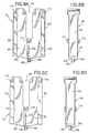
- A module (40, 40A) for use with a modular card edge electrical connector according to claim 1 characterized in that the insulative housing (54) has an outer peripheral surface (82) with first and second opposed major sides (94, 96) and a first minor side (98) joining the first and second major sides, and having third and fourth opposed major sides (100, 102) and a second minor side (104) joining the first and second major sides (94, 96), the first and third major sides (94, 100) being coplanar, the second and fourth major sides (96, 102) being coplanar, the first and second minor sides (98, 104) lying in parallel spaced apart planes, the insulative frame having a first elongated slot (106) spaced from and aligned with the card receiving recess (60) and having an inlet positioned intermediate the first and third major sides (94, 100), the first elongated slot (106) being generally parallel with the first and second minor sides (98, 104), the insulative frame having a second elongated slot (107) spaced from and aligned with the card receiving recess (60) and having an inlet positioned intermediate the second and fourth major sides (96, 102), the second elongated slot (107) being generally parallel with the first and second minor sides (98, 104); and including:first and second ground shields (78, 80), each having a C-shaped cross section, slidably received, respectively, on the insulative housing (54) in opposed relationship and in proximate engagement with the outer peripheral surface (82), the first ground shield (78) generally overlying the first elongated passage (56, 56A), the second ground shield (80) generally overlying the second elongated passage (58, 58A), the first ground shield (78) having first and second opposed limbs (108, 110) proximately overlying the first and second major sides (94, 96), respectively, a first side limb (112) proximately overlying the first minor side (98), and a first flange limb (114) extending transverse of the first opposed limb slidably received in the first elongated slot (106) whereby the first ground shield (78) substantially completely surrounds the first elongated contact (62) received in the first passage (56, 56A), the second ground shield (80) having third and fourth opposed limbs (116, 118) proximately overlying the third and fourth major sides (100, 102), respectively, a second side limb (120) proximately overlying the second minor side (104), and a second flange limb (122) extending transverse of the third opposed limb slidably received in the second elongated slot (107) whereby the second ground shield (80) substantially completely surrounds the second elongated contact (66) received in the second passage (58, 58A), the first and second ground shields (78, 80) both including a first integral ground contact (84) for engagement with a ground contact (86) of an external unit (26) associated with the mating contacts (22) engaged by the first contact surfaces (64, 68) of the first and second elongated contacts (62, 66), each of the first and second ground shields (78, 80) including a second integral ground contact (88) for engagement with an associated ground contact surface (90) on the planar card (28, 28A) inserted into the card receiving slot (70).
- A module (40, 40A) for use with a modular card edge electrical connector according to claim 2, characterized in that both of the second integral ground contacts (88) of the first and second ground shields (78, 80) project into the card receiving recess (60); and that
the second integral ground contact (88) of the first ground shield (78) generally faces the second integral ground contact (88) of the second ground shield (80). - A module (40, 40A) for use with a modular card edge electrical connector according to claim 2, characterized in that the second integral ground contacts of the first and second ground shields (78, 80) project into the card receiving recess (60) at a location nearer the top wall (46, 46A) of the outer frame (36) than either of the second contact surfaces (64, 68) of the first and second elongated contacts (62, 66) to establish an early mate, last break, grounding operation.
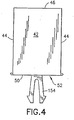
- A module (40, 40A) for use with a modular card edge electrical connector according to claim 1, characterized in that each module (40, 40A) has locating features (142) formed for engagement with complementary locating features (144) of an outer frame (36) such that each module (40, 40A) is positively positioned with respect to the outer frame (36).
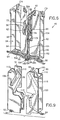
- A module according to claim 2, including:a bridging contact (180) on at least one of the ground shields (78, 80) of one of the chiclet module (40, 40A) engageable with the ground shield of its adjoining chiclet module (40, 40A).
- A module according to claim 2, including:at least one boss member (174) on the insulative housing (54) of one module (40, 40A) engageable with the insulative housing (54) of an adjoining module (40, 40A), the boss member (174) dimensioned to prevent mutual engagement of the ground shields (78, 80) of the adjoining modules (40, 40A).
- A module according to claim 2, including:a plurality of mutually opposed pairs of boss members (174) on the insulative housings of adjoining modules (40, 40A), such mutually opposed pairs of boss members (174) being engaged and dimensioned to prevent mutual engagement of the ground shields (78, 80) of the adjoining modules (40, 40A).
- A module according to claim 2, characterized in that the tubular ground shield (128) or each of the first and second ground shields (78, 80) has a cutout region (92) enabling visual inspection of the first contact surfaces (64, 68) of the first and second elongated contacts (62, 66) when engaged with the first and second of the mating contacts (22), respectively, and of the first ground contacts (84) when engaged with the mating ground contacts of the external unit (26).
- A module according to claim 1, characterized in that the insulative housing (54) has an outer peripheral surface (82); and including:a tubular ground shield (128) slidably received on the insulative housing (54) in proximate engagement with the outer peripheral surface (82), the ground shield including:a first integral ground contact (84) for engagement with a ground contact (86) of an external unit (26) associated with the mating contacts (22) engaged by the first contact surfaces (64) of the first and second contacts (62, 66); anda second integral ground contact (88) for engagement with a ground contact surface (86) on the planar card (28, 28A) inserted into the card receiving slot (70).
- A module according to claim 11, characterized in that the tubular ground shield (128) has a cutout region (92) enabling visual inspection of the first contact surfaces (64) of the first and second contacts (62, 66) when engaged with the first and second of the mating contacts (22), respectively, and of the first and second ground contacts (84, 88) when engaged with the mating ground contacts (86) of the external unit (26).
- A module according to claim 1, characterized in that the insulative housing (54) has an outer peripheral surface (82); and including:first and second ground shields (78, 80), each having a C-shaped cross section, slidably received, respectively, on the insulative housing (54) in opposed relationship and in proximate engagement with the outer peripheral surface (82), the first ground shield (78) generally overlying the first elongated passage (56, 56A), the second ground shield (80) generally overlying the second elongated passage (58, 58A), the first and second ground shields (78, 80) both including a first integral ground contact (84) for engagement with a ground contact (86) of an external unit (26) associated with the mating contacts (22) engaged by the first contact surfaces (64) of the first and second contacts (62, 66), each of the first and second ground shields (78, 80) including a second integral ground contact (88) for engagement with an associated ground contact surface (90) on the planar card (28, 28A) inserted into the card receiving slot (70).
- A module according to claim 13, characterized in that each of the first and second ground shields (78, 80) has a cutout region (92) enabling visual inspection of the first contact surfaces (64) of the first and second contacts (62, 66) when engaged with the first and second of the mating contacts (22), respectively, and of the first and second ground contacts (84, 88) when engaged with the mating ground contacts of the external unit (26).
- A module according to claim 13 including:at least one boss member (174) on the insulative housing (54) of one module (40, 40A) engageable with the insulative housing (54) of an adjoining module (40, 40A), the boss member (174) dimensioned to prevent mutual engagement of the ground shields of the adjoining modules (40, 40A).
- A module according to claim 1, characterized in that the insulative housing (54) has an outer peripheral surface (82); and including:first and second ground shields (78, 80), each having a C-shaped cross section, slidably received, respectively, on the insulative housing (54) in opposed relationship and in proximate engagement with the outer peripheral surface (82), the first ground shield (78) generally overlying the first elongated passage (56, 56A), the second ground shield (80) generally overlying the second elongated passage (58, 58A), the first and second ground shields (78, 80) both including a first integral ground contact (84) for engagement with a ground contact (86) of an external unit (26) associated with the mating contacts (22) engaged by the first contact surfaces (64) of the first and second contacts (62, 66), each of the first and second ground shields (78, 80) including a second integral ground contact (88) for engagement with an associated ground contact surface (90) on the planar card (28, 28A) inserted into the card receiving recess (60).
- A module according to claim 11, characterized in that the insulative housing (54) has an outer peripheral surface (82) with first and second opposed major sides (94, 96) and a first minor side (98) joining the first and second major sides, and having third and fourth opposed major sides (100, 102) and a second minor side (104) joining the first and second major sides, the first and third major sides (94, 100) being coplanar, the second and fourth major sides being coplanar, the first and second minor sides (98, 104) lying in parallel spaced apart planes, the insulative frame having a first elongated slot (106) spaced from and aligned with the card receiving recess (60) and having an inlet positioned intermediate the first and third major sides (94, 100), the first elongated slot (106) being generally parallel with the first and second minor sides (98, 104), the insulative frame having a second elongated slot (107) spaced from and aligned with the card receiving recess (60) and having an inlet positioned intermediate the second and fourth major sides, the second elongated slot (107) being generally parallel with the first and second minor sides (98, 104); and including:first and second ground shields (78, 80), each having a C-shaped cross section, slidably received, respectively, on the insulative housing (54) in opposed relationship and in proximate engagement with the outer peripheral surface (82), the first ground shield (78) generally overlying the first elongated passage (56, 56A), the second ground shield (80) generally overlying the second elongated passage (58, 58A), the first ground shield (78) having first and second opposed limbs (108, 110) proximately overlying the first and second major sides, respectively, a first side limb (112) proximately overlying the first minor side (98), and a first flange limb (114) extending transverse of the first opposed limb slidably received in the first elongated slot (106) whereby the first ground shield (78) substantially completely surrounds the first contact (62) received in the first passage (56, 56A), the second ground shield (80) having third and fourth opposed limbs (116, 118) proximately overlying the third and fourth major sides, respectively, a second side limb (120) proximately overlying the second minor side (104), and a second flange limb (122) extending transverse of the third opposed limb slidably received in the first elongated slot (106) whereby the second ground shield (80) substantially completely surrounds the second contact (66) received in the second passage (58, 58A), the first and second ground shields (78, 80) both including a firstintegral ground contact (84) for engagement with a ground contact (86) of an external unit (26) associated with the mating contacts (22) engaged by the first contact surfaces (64) of the first and second contacts (62, 66), each of the first and second ground shields (78, 80) including a second integral ground contact (88) for engagement with an associated ground contact surface (90) on the planarcard (28, 28A) inserted into the card receiving slot (70).
- A module according to claim 16, characterized in that both of the second integral ground contacts of the first and second ground shields (78, 80) project into the card receiving recess (60); and that the second integral ground contact (88) of the first ground shield (78) generally faces the second integral ground contact (88) of the second ground shield (80).
- A module according to claim 16, characterized in that the second integral ground contacts of the first and second ground shields (78, 80) project into the card receiving slot (70) at a location nearer the top wall (46, 46A) of the outer frame (36) than either of the second contact surfaces (68) of the first and second contacts (62, 66) to establish an early mate, last break, grounding operation.
Applications Claiming Priority (2)
| Application Number | Priority Date | Filing Date | Title |
|---|---|---|---|
| US09/474,818 US6464537B1 (en) | 1999-12-29 | 1999-12-29 | High speed card edge connectors |
| US474818 | 1999-12-29 |
Publications (3)
| Publication Number | Publication Date |
|---|---|
| EP1113530A2 EP1113530A2 (en) | 2001-07-04 |
| EP1113530A3 EP1113530A3 (en) | 2003-05-21 |
| EP1113530B1 true EP1113530B1 (en) | 2005-11-23 |
Family
ID=23885063
Family Applications (1)
| Application Number | Title | Priority Date | Filing Date |
|---|---|---|---|
| EP00128102A Expired - Lifetime EP1113530B1 (en) | 1999-12-29 | 2000-12-21 | High speed card edge connectors |
Country Status (8)
| Country | Link |
|---|---|
| US (2) | US6464537B1 (en) |
| EP (1) | EP1113530B1 (en) |
| JP (1) | JP2001196128A (en) |
| KR (1) | KR100730272B1 (en) |
| AT (1) | ATE311023T1 (en) |
| CA (1) | CA2329677A1 (en) |
| DE (1) | DE60024212T2 (en) |
| TW (1) | TW530434B (en) |
Cited By (2)
| Publication number | Priority date | Publication date | Assignee | Title |
|---|---|---|---|---|
| CN102255201A (en) * | 2010-02-12 | 2011-11-23 | 泰科电子公司 | Socket connector with ground shields between ajacent signal contacts |
| TWI412185B (en) * | 2011-01-14 | 2013-10-11 | Alltop Technology Co Ltd | Card-edge connector and assembly thereof |
Families Citing this family (46)
| Publication number | Priority date | Publication date | Assignee | Title |
|---|---|---|---|---|
| CN1305354C (en) * | 2001-10-10 | 2007-03-14 | 莫莱克斯公司 | High speed differential signal edge card connector and circuit board layouts therefor |
| US6685485B2 (en) * | 2002-03-07 | 2004-02-03 | Hon Hai Precision Ind. Co., Ltd. | Electrical connector |
| US7040934B2 (en) * | 2002-12-19 | 2006-05-09 | Intel Corporation | Add-in card to backplane connecting apparatus |
| JP3841348B2 (en) * | 2003-02-25 | 2006-11-01 | 日本航空電子工業株式会社 | Connector ground structure |
| US6843687B2 (en) * | 2003-02-27 | 2005-01-18 | Molex Incorporated | Pseudo-coaxial wafer assembly for connector |
| US7083432B2 (en) * | 2003-08-06 | 2006-08-01 | Fci Americas Technology, Inc. | Retention member for connector system |
| US7048585B2 (en) * | 2003-12-23 | 2006-05-23 | Teradyne, Inc. | High speed connector assembly |
| JP4215696B2 (en) * | 2004-08-27 | 2009-01-28 | ヒロセ電機株式会社 | Multi-pole connector |
| ATE451793T1 (en) * | 2005-02-03 | 2009-12-15 | 3M Innovative Properties Co | FUNCTIONAL MODULE AND ARRANGEMENT COMPRISING AT LEAST ONE TELECOMMUNICATIONS MODULE AND AT LEAST ONE FUNCTIONAL MODULE |
| US7172465B2 (en) * | 2005-02-22 | 2007-02-06 | Micron Technology, Inc. | Edge connector including internal layer contact, printed circuit board and electronic module incorporating same |
| CN2809939Y (en) * | 2005-05-20 | 2006-08-23 | 富士康(昆山)电脑接插件有限公司 | Electric connector |
| US20070048709A1 (en) * | 2005-08-31 | 2007-03-01 | Kimberly-Clark Worldwide, Inc. | System for detection and analysis of biological waste spread in an undergarment |
| US7239528B1 (en) | 2005-10-05 | 2007-07-03 | Cisco Technology, Inc. | Techniques for accommodating variations in chassis tolerances |
| US7410392B2 (en) * | 2005-12-15 | 2008-08-12 | Tyco Electronics Corporation | Electrical connector assembly having selective arrangement of signal and ground contacts |
| US7150652B1 (en) * | 2006-02-21 | 2006-12-19 | Myoungsoo Jeon | Connector having a pair of printed circuits and facing sets of contact beams |
| TW200812156A (en) * | 2006-08-21 | 2008-03-01 | Speed Tech Corp | High destiny electrical connector and method for assembling thereof |
| US7588468B2 (en) * | 2006-08-24 | 2009-09-15 | Hon Hai Precision Ind. Co., Ltd. | Electrical connector with improved preloading structure |
| JP4560026B2 (en) * | 2006-10-04 | 2010-10-13 | セイコーエプソン株式会社 | Flexible substrate, electro-optical device including the same, and electronic apparatus |
| US7472477B2 (en) * | 2006-10-12 | 2009-01-06 | International Business Machines Corporation | Method for manufacturing a socket that compensates for differing coefficients of thermal expansion |
| TWM363133U (en) * | 2008-11-28 | 2009-08-11 | Nextronics Engineering Corp | Press-contact electrical connector |
| TWM358444U (en) * | 2008-12-30 | 2009-06-01 | Advanced Connectek Inc | Electric connector suitable for transmitting a high-frequency signal |
| US8740647B1 (en) * | 2010-02-02 | 2014-06-03 | Arris Enterprises, Inc. | Reduced crosstalk in a multi-channel conductive body connector |
| JP5009388B2 (en) * | 2010-02-18 | 2012-08-22 | パナソニック株式会社 | Receptacle, printed wiring board, and electronic equipment |
| JP4638960B1 (en) * | 2010-02-18 | 2011-02-23 | パナソニック株式会社 | Receptacle, printed wiring board, and electronic equipment |
| US8267728B2 (en) | 2010-02-18 | 2012-09-18 | Panasonic Corporation | Receptacle, printed wiring board, and electronic device |
| TWM396512U (en) * | 2010-07-30 | 2011-01-11 | Tyco Electronics Holdings Bermuda No 7 Ltd | Card-edge connector |
| US8747164B2 (en) * | 2011-03-01 | 2014-06-10 | Tyco Electronics Corporation | Card edge connector |
| US8231411B1 (en) * | 2011-03-01 | 2012-07-31 | Tyco Electronics Corporation | Card edge connector |
| SG185162A1 (en) * | 2011-04-28 | 2012-11-29 | 3M Innovative Properties Co | An electrical connector |
| US8419457B2 (en) * | 2011-08-26 | 2013-04-16 | Concraft Holding Co., Ltd. | Anti-electromagnetic interference electrical connector and terminal assembly thereof |
| US8727809B2 (en) * | 2011-09-06 | 2014-05-20 | Samtec, Inc. | Center conductor with surrounding shield and edge card connector with same |
| US9065225B2 (en) * | 2012-04-26 | 2015-06-23 | Apple Inc. | Edge connector having a high-density of contacts |
| US8944850B2 (en) * | 2012-10-22 | 2015-02-03 | Apple Inc. | Shielding for edge connector |
| US10198389B2 (en) * | 2014-07-14 | 2019-02-05 | Cavium, Llc | Baseboard interconnection device, system and method |
| US9989990B2 (en) * | 2014-12-18 | 2018-06-05 | Dell Prodcuts L.P. | Connector with staggered electrical pins |
| US9692183B2 (en) * | 2015-01-20 | 2017-06-27 | Te Connectivity Corporation | Receptacle connector with ground bus |
| JP6530976B2 (en) * | 2015-06-24 | 2019-06-12 | イリソ電子工業株式会社 | Connector cap |
| TWI713271B (en) * | 2015-12-18 | 2020-12-11 | 日商廣瀨電機股份有限公司 | Connector and manufacturing method thereof |
| US9929511B2 (en) | 2016-03-18 | 2018-03-27 | Intel Corporation | Shielded high density card connector |
| JP6765243B2 (en) * | 2016-07-14 | 2020-10-07 | ヒロセ電機株式会社 | Electrical connector |
| CN112368892B (en) * | 2018-06-27 | 2022-05-13 | 株式会社村田制作所 | Electric connector set |
| CN109586067B (en) * | 2018-10-23 | 2020-06-09 | 番禺得意精密电子工业有限公司 | Electrical connector |
| US11233348B2 (en) * | 2020-04-24 | 2022-01-25 | Intel Corporation | Structural optimization of contact geometry for high performance connector |
| JP2022186325A (en) * | 2021-06-04 | 2022-12-15 | 日立チャネルソリューションズ株式会社 | Card reader and foreign object detection method for card reader |
| JP2023138066A (en) * | 2022-03-18 | 2023-09-29 | イリソ電子工業株式会社 | connector |
| TWI812513B (en) * | 2022-10-18 | 2023-08-11 | 國立臺北科技大學 | Card edge connector with resonance-improving structure and method for assembly thereof |
Family Cites Families (59)
| Publication number | Priority date | Publication date | Assignee | Title |
|---|---|---|---|---|
| US2879491A (en) | 1954-08-12 | 1959-03-24 | Shapiro Gustave | Plug system for joining electric subassembly to chassis |
| NL135885C (en) | 1962-06-18 | 1900-01-01 | ||
| GB1185674A (en) * | 1966-03-17 | 1970-03-25 | Elco Corp | Improvements in or relating to Electrical Contacts |
| US3399372A (en) | 1966-04-15 | 1968-08-27 | Ibm | High density connector package |
| US3516046A (en) | 1968-02-27 | 1970-06-02 | William A Gettig | Edge connector for printed circuit board |
| US3992072A (en) * | 1976-02-23 | 1976-11-16 | International Telephone And Telegraph Corporation | Electrical connector |
| US4067637A (en) | 1976-12-09 | 1978-01-10 | Thomas & Betts Corporation | Electrical connector |
| US4324451A (en) | 1979-11-19 | 1982-04-13 | Elfab Corporation | Card edge connector with pull through bellows contact and lay-over insulator |
| US4343528A (en) | 1980-04-25 | 1982-08-10 | Amp Incorporated | Modular interconnect system |
| AU8553682A (en) | 1981-07-08 | 1983-01-13 | Poland, J.M. | Edge connector 0 |
| US4550959A (en) | 1983-04-13 | 1985-11-05 | Amp Incorporated | Surface mountable coefficient of expansion matching connector |
| DE3373256D1 (en) | 1983-05-19 | 1987-10-01 | Ibm Deutschland | Process for manufacturing printed circuits with metallic conductor patterns embedded in the isolating substrate |
| US4586254A (en) | 1983-08-05 | 1986-05-06 | Elfab Corp. | Method of making a modular connector |
| US4556268A (en) * | 1983-11-23 | 1985-12-03 | Burndy Corporation | Circuit board connector system having independent contact segments |
| US4596436A (en) | 1985-03-25 | 1986-06-24 | Amp Incorporated | Electrical connector housing assembly comprising housing frame containing housing modules |
| JPS6210885A (en) | 1985-07-08 | 1987-01-19 | 日本航空電子工業株式会社 | Connector |
| US5013263A (en) | 1985-11-22 | 1991-05-07 | William Gordon | Modular electrical connector structure |
| US4663552A (en) * | 1986-02-26 | 1987-05-05 | General Electric Company | Ganged inside-out brushholder for dynamoelectric machine |
| US4820169A (en) | 1986-04-22 | 1989-04-11 | Amp Incorporated | Programmable modular connector assembly |
| US5169324A (en) | 1986-11-18 | 1992-12-08 | Lemke Timothy A | Plug terminator having a grounding member |
| US5057028A (en) | 1986-11-18 | 1991-10-15 | E. I. Du Pont De Nemours And Company | Receptacle having a nosepeice to receive cantilevered spring contacts |
| US4891023A (en) * | 1988-08-22 | 1990-01-02 | Molex Incorporated | Circuit card edge connector and terminal therefor |
| US4883432A (en) | 1988-12-28 | 1989-11-28 | The Siemon Company | Modular jack yoke |
| JP2896783B2 (en) | 1989-03-01 | 1999-05-31 | 日本航空電子工業株式会社 | Double lock structure of connector housing |
| US4892487A (en) | 1989-06-15 | 1990-01-09 | Ibm Corporation | Connector assembly with movable carriage |
| GB8928777D0 (en) | 1989-12-20 | 1990-02-28 | Amp Holland | Sheilded backplane connector |
| US5090911A (en) | 1990-01-11 | 1992-02-25 | Itt Corporation | Modular connector system |
| US5024609A (en) | 1990-04-04 | 1991-06-18 | Burndy Corporation | High-density bi-level card edge connector and method of making the same |
| US5035631A (en) * | 1990-06-01 | 1991-07-30 | Burndy Corporation | Ground shielded bi-level card edge connector |
| US5096435A (en) | 1991-01-03 | 1992-03-17 | Burndy Corporation | Bi-level card edge connector with selectively movable contacts for use with different types of cards |
| US5184961A (en) | 1991-06-20 | 1993-02-09 | Burndy Corporation | Modular connector frame |
| JPH0521110A (en) * | 1991-07-10 | 1993-01-29 | Amp Japan Ltd | Shielding type electric connector |
| US5125854A (en) | 1991-07-16 | 1992-06-30 | Molex Incorporated | Modular electrical connector |
| US5145411A (en) | 1991-08-14 | 1992-09-08 | Amp Incorporated | Connector insert retention system |
| NL9200559A (en) | 1992-03-26 | 1993-10-18 | Du Pont Nederland | CONNECTOR. |
| US5221218A (en) * | 1992-07-17 | 1993-06-22 | Cooper Industries, Inc. | Edge-card connector |
| US5308248A (en) | 1992-08-31 | 1994-05-03 | International Business Machines Corp. | High density interconnection system |
| JPH0629066U (en) | 1992-09-21 | 1994-04-15 | 京セラエルコ株式会社 | Edge double-sided connector |
| US5443403A (en) | 1993-03-10 | 1995-08-22 | The Whitaker Corporation | Composite electrical connector assembly with snap-in housing |
| US5403206A (en) * | 1993-04-05 | 1995-04-04 | Teradyne, Inc. | Shielded electrical connector |
| US5496180A (en) * | 1994-04-06 | 1996-03-05 | The Whitaker Corporation | Surface mountable card edge connector |
| US5443394A (en) * | 1994-05-04 | 1995-08-22 | The Whitaker Corporation | Card edge connector having positive lock and extractor |
| US5445531A (en) | 1994-08-23 | 1995-08-29 | The Whitaker Corporation | Card edge connector with shim lock and extractor mechanism |
| JP3685210B2 (en) * | 1994-11-11 | 2005-08-17 | ケル株式会社 | connector |
| US5584728A (en) | 1994-11-25 | 1996-12-17 | Hon Hai Precision Ind. Co., Ltd. | Modular connector assembly with variably positioned units |
| US5704793A (en) | 1995-04-17 | 1998-01-06 | Teradyne, Inc. | High speed high density connector for electronic signals |
| US5580257A (en) * | 1995-04-28 | 1996-12-03 | Molex Incorporated | High performance card edge connector |
| US5725389A (en) * | 1995-11-09 | 1998-03-10 | Molex Incorporated | Edge card connector |
| DE29602740U1 (en) | 1996-02-21 | 1996-04-11 | Phoenix Contact Gmbh & Co | Electrical connector |
| US5716237A (en) | 1996-06-21 | 1998-02-10 | Lucent Technologies Inc. | Electrical connector with crosstalk compensation |
| US5785537A (en) * | 1996-06-26 | 1998-07-28 | Robinson Nugent, Inc. | Electrical connector interlocking apparatus |
| US5882214A (en) | 1996-06-28 | 1999-03-16 | The Whitaker Corporation | Electrical connector with contact assembly |
| US5785556A (en) * | 1996-07-16 | 1998-07-28 | Molex Incorporated | Edge connector for a printed circuit board |
| TW329992U (en) * | 1996-11-18 | 1998-04-11 | Hon Hai Prec Ind Co Ltd | Connector ejecting device |
| US5876214A (en) * | 1996-12-30 | 1999-03-02 | Hon Hai Precision Ind. Co., Ltd. | Grounding structure for use with card edge connector |
| JP2002500810A (en) * | 1997-05-27 | 2002-01-08 | ザ ウィタカー コーポレーション | Card edge connectors and contacts |
| US5924898A (en) | 1997-05-29 | 1999-07-20 | Raychem Corporation | Modular connector |
| DE19730484C1 (en) * | 1997-07-16 | 1998-10-22 | Siemens Ag | Circuit boards zero insertion force connector arrangement |
| NL1009530C2 (en) * | 1998-06-30 | 2000-01-04 | Framatome Connectors Belgium | Connector. |
-
1999
- 1999-12-29 US US09/474,818 patent/US6464537B1/en not_active Expired - Fee Related
-
2000
- 2000-12-13 TW TW089126607A patent/TW530434B/en not_active IP Right Cessation
- 2000-12-21 AT AT00128102T patent/ATE311023T1/en not_active IP Right Cessation
- 2000-12-21 EP EP00128102A patent/EP1113530B1/en not_active Expired - Lifetime
- 2000-12-21 DE DE60024212T patent/DE60024212T2/en not_active Expired - Fee Related
- 2000-12-22 JP JP2000391490A patent/JP2001196128A/en not_active Withdrawn
- 2000-12-27 CA CA002329677A patent/CA2329677A1/en not_active Abandoned
- 2000-12-28 KR KR1020000083465A patent/KR100730272B1/en not_active IP Right Cessation
-
2002
- 2002-08-27 US US10/229,736 patent/US6561850B2/en not_active Expired - Fee Related
Cited By (3)
| Publication number | Priority date | Publication date | Assignee | Title |
|---|---|---|---|---|
| CN102255201A (en) * | 2010-02-12 | 2011-11-23 | 泰科电子公司 | Socket connector with ground shields between ajacent signal contacts |
| CN102255201B (en) * | 2010-02-12 | 2016-05-25 | 泰科电子公司 | Between adjacent signal contact, there is the socket connector of ground shield |
| TWI412185B (en) * | 2011-01-14 | 2013-10-11 | Alltop Technology Co Ltd | Card-edge connector and assembly thereof |
Also Published As
| Publication number | Publication date |
|---|---|
| DE60024212D1 (en) | 2005-12-29 |
| KR100730272B1 (en) | 2007-06-19 |
| KR20010062793A (en) | 2001-07-07 |
| ATE311023T1 (en) | 2005-12-15 |
| US20030003804A1 (en) | 2003-01-02 |
| US6561850B2 (en) | 2003-05-13 |
| US6464537B1 (en) | 2002-10-15 |
| TW530434B (en) | 2003-05-01 |
| JP2001196128A (en) | 2001-07-19 |
| EP1113530A2 (en) | 2001-07-04 |
| DE60024212T2 (en) | 2006-07-20 |
| CA2329677A1 (en) | 2001-06-29 |
| EP1113530A3 (en) | 2003-05-21 |
Similar Documents
| Publication | Publication Date | Title |
|---|---|---|
| EP1113530B1 (en) | High speed card edge connectors | |
| US9923309B1 (en) | PCB connector footprint | |
| US4975084A (en) | Electrical connector system | |
| EP0757851B1 (en) | Conductive shroud for electrical connectors | |
| EP0459356B1 (en) | Ground shielded bi-level card edge connector | |
| US5104341A (en) | Shielded backplane connector | |
| EP0670616B1 (en) | Connector for a cable for high frequency signals | |
| US5664968A (en) | Connector assembly with shielded modules | |
| EP1190469B1 (en) | Modular electrical connector and connector system | |
| US6371773B1 (en) | High density interconnect system and method | |
| EP0422785B1 (en) | Impedance matched backplane connector | |
| EP0746060A2 (en) | Shielded back plane connector | |
| KR970001948B1 (en) | Integral ground terminal and tail shield | |
| EP0390295B1 (en) | Connector with means for securing to a substrate | |
| EP0365179B1 (en) | Electrical connector system | |
| EP1207587A2 (en) | High speed card edge connectors | |
| US6468090B2 (en) | Low inductance power connector and method of reducing inductance in an electrical connector | |
| EP3435495B1 (en) | Electrical connector with improved impedance characteristics | |
| US7967636B2 (en) | Electrical connector with terminals staggered from each other | |
| EP1294055B1 (en) | Connector assembly comprising a tab-receiving insulated spring sleeve and a dual contact with pairs of spaced apart contact members and tails |
Legal Events
| Date | Code | Title | Description |
|---|---|---|---|
| PUAI | Public reference made under article 153(3) epc to a published international application that has entered the european phase |
Free format text: ORIGINAL CODE: 0009012 |
|
| AK | Designated contracting states |
Kind code of ref document: A2 Designated state(s): AT BE CH CY DE DK ES FI FR GB GR IE IT LI LU MC NL PT SE TR |
|
| AX | Request for extension of the european patent |
Free format text: AL;LT;LV;MK;RO;SI |
|
| PUAL | Search report despatched |
Free format text: ORIGINAL CODE: 0009013 |
|
| AK | Designated contracting states |
Designated state(s): AT BE CH CY DE DK ES FI FR GB GR IE IT LI LU MC NL PT SE TR |
|
| AX | Request for extension of the european patent |
Extension state: AL LT LV MK RO SI |
|
| 17P | Request for examination filed |
Effective date: 20030919 |
|
| 17Q | First examination report despatched |
Effective date: 20031216 |
|
| AKX | Designation fees paid |
Designated state(s): AT BE CH CY DE DK ES FI FR GB GR IE IT LI LU MC NL PT SE TR |
|
| GRAP | Despatch of communication of intention to grant a patent |
Free format text: ORIGINAL CODE: EPIDOSNIGR1 |
|
| GRAS | Grant fee paid |
Free format text: ORIGINAL CODE: EPIDOSNIGR3 |
|
| GRAA | (expected) grant |
Free format text: ORIGINAL CODE: 0009210 |
|
| RAP1 | Party data changed (applicant data changed or rights of an application transferred) |
Owner name: FCI |
|
| AK | Designated contracting states |
Kind code of ref document: B1 Designated state(s): AT BE CH CY DE DK ES FI FR GB GR IE IT LI LU MC NL PT SE TR |
|
| PG25 | Lapsed in a contracting state [announced via postgrant information from national office to epo] |
Ref country code: IT Free format text: LAPSE BECAUSE OF FAILURE TO SUBMIT A TRANSLATION OF THE DESCRIPTION OR TO PAY THE FEE WITHIN THE PRESCRIBED TIME-LIMIT;WARNING: LAPSES OF ITALIAN PATENTS WITH EFFECTIVE DATE BEFORE 2007 MAY HAVE OCCURRED AT ANY TIME BEFORE 2007. THE CORRECT EFFECTIVE DATE MAY BE DIFFERENT FROM THE ONE RECORDED. Effective date: 20051123 Ref country code: AT Free format text: LAPSE BECAUSE OF FAILURE TO SUBMIT A TRANSLATION OF THE DESCRIPTION OR TO PAY THE FEE WITHIN THE PRESCRIBED TIME-LIMIT Effective date: 20051123 Ref country code: BE Free format text: LAPSE BECAUSE OF FAILURE TO SUBMIT A TRANSLATION OF THE DESCRIPTION OR TO PAY THE FEE WITHIN THE PRESCRIBED TIME-LIMIT Effective date: 20051123 Ref country code: FI Free format text: LAPSE BECAUSE OF FAILURE TO SUBMIT A TRANSLATION OF THE DESCRIPTION OR TO PAY THE FEE WITHIN THE PRESCRIBED TIME-LIMIT Effective date: 20051123 Ref country code: TR Free format text: LAPSE BECAUSE OF FAILURE TO SUBMIT A TRANSLATION OF THE DESCRIPTION OR TO PAY THE FEE WITHIN THE PRESCRIBED TIME-LIMIT Effective date: 20051123 Ref country code: NL Free format text: LAPSE BECAUSE OF FAILURE TO SUBMIT A TRANSLATION OF THE DESCRIPTION OR TO PAY THE FEE WITHIN THE PRESCRIBED TIME-LIMIT Effective date: 20051123 Ref country code: CH Free format text: LAPSE BECAUSE OF FAILURE TO SUBMIT A TRANSLATION OF THE DESCRIPTION OR TO PAY THE FEE WITHIN THE PRESCRIBED TIME-LIMIT Effective date: 20051123 Ref country code: LI Free format text: LAPSE BECAUSE OF FAILURE TO SUBMIT A TRANSLATION OF THE DESCRIPTION OR TO PAY THE FEE WITHIN THE PRESCRIBED TIME-LIMIT Effective date: 20051123 |
|
| REG | Reference to a national code |
Ref country code: GB Ref legal event code: FG4D |
|
| REG | Reference to a national code |
Ref country code: CH Ref legal event code: EP |
|
| PG25 | Lapsed in a contracting state [announced via postgrant information from national office to epo] |
Ref country code: IE Free format text: LAPSE BECAUSE OF NON-PAYMENT OF DUE FEES Effective date: 20051221 Ref country code: CY Free format text: LAPSE BECAUSE OF FAILURE TO SUBMIT A TRANSLATION OF THE DESCRIPTION OR TO PAY THE FEE WITHIN THE PRESCRIBED TIME-LIMIT Effective date: 20051221 |
|
| REF | Corresponds to: |
Ref document number: 60024212 Country of ref document: DE Date of ref document: 20051229 Kind code of ref document: P |
|
| REG | Reference to a national code |
Ref country code: IE Ref legal event code: FG4D |
|
| PG25 | Lapsed in a contracting state [announced via postgrant information from national office to epo] |
Ref country code: MC Free format text: LAPSE BECAUSE OF NON-PAYMENT OF DUE FEES Effective date: 20051231 |
|
| PG25 | Lapsed in a contracting state [announced via postgrant information from national office to epo] |
Ref country code: LU Free format text: LAPSE BECAUSE OF NON-PAYMENT OF DUE FEES Effective date: 20060123 |
|
| PG25 | Lapsed in a contracting state [announced via postgrant information from national office to epo] |
Ref country code: SE Free format text: LAPSE BECAUSE OF FAILURE TO SUBMIT A TRANSLATION OF THE DESCRIPTION OR TO PAY THE FEE WITHIN THE PRESCRIBED TIME-LIMIT Effective date: 20060223 Ref country code: GR Free format text: LAPSE BECAUSE OF FAILURE TO SUBMIT A TRANSLATION OF THE DESCRIPTION OR TO PAY THE FEE WITHIN THE PRESCRIBED TIME-LIMIT Effective date: 20060223 Ref country code: DK Free format text: LAPSE BECAUSE OF FAILURE TO SUBMIT A TRANSLATION OF THE DESCRIPTION OR TO PAY THE FEE WITHIN THE PRESCRIBED TIME-LIMIT Effective date: 20060223 |
|
| PG25 | Lapsed in a contracting state [announced via postgrant information from national office to epo] |
Ref country code: ES Free format text: LAPSE BECAUSE OF FAILURE TO SUBMIT A TRANSLATION OF THE DESCRIPTION OR TO PAY THE FEE WITHIN THE PRESCRIBED TIME-LIMIT Effective date: 20060306 |
|
| PG25 | Lapsed in a contracting state [announced via postgrant information from national office to epo] |
Ref country code: PT Free format text: LAPSE BECAUSE OF FAILURE TO SUBMIT A TRANSLATION OF THE DESCRIPTION OR TO PAY THE FEE WITHIN THE PRESCRIBED TIME-LIMIT Effective date: 20060424 |
|
| NLV1 | Nl: lapsed or annulled due to failure to fulfill the requirements of art. 29p and 29m of the patents act | ||
| ET | Fr: translation filed | ||
| REG | Reference to a national code |
Ref country code: CH Ref legal event code: PL |
|
| PLBE | No opposition filed within time limit |
Free format text: ORIGINAL CODE: 0009261 |
|
| STAA | Information on the status of an ep patent application or granted ep patent |
Free format text: STATUS: NO OPPOSITION FILED WITHIN TIME LIMIT |
|
| REG | Reference to a national code |
Ref country code: IE Ref legal event code: MM4A |
|
| 26N | No opposition filed |
Effective date: 20060824 |
|
| PGFP | Annual fee paid to national office [announced via postgrant information from national office to epo] |
Ref country code: GB Payment date: 20071106 Year of fee payment: 8 |
|
| PGFP | Annual fee paid to national office [announced via postgrant information from national office to epo] |
Ref country code: DE Payment date: 20071228 Year of fee payment: 8 |
|
| PGFP | Annual fee paid to national office [announced via postgrant information from national office to epo] |
Ref country code: FR Payment date: 20071204 Year of fee payment: 8 |
|
| GBPC | Gb: european patent ceased through non-payment of renewal fee |
Effective date: 20081221 |
|
| REG | Reference to a national code |
Ref country code: FR Ref legal event code: ST Effective date: 20090831 |
|
| PG25 | Lapsed in a contracting state [announced via postgrant information from national office to epo] |
Ref country code: DE Free format text: LAPSE BECAUSE OF NON-PAYMENT OF DUE FEES Effective date: 20090701 |
|
| PG25 | Lapsed in a contracting state [announced via postgrant information from national office to epo] |
Ref country code: GB Free format text: LAPSE BECAUSE OF NON-PAYMENT OF DUE FEES Effective date: 20081221 |
|
| PG25 | Lapsed in a contracting state [announced via postgrant information from national office to epo] |
Ref country code: FR Free format text: LAPSE BECAUSE OF NON-PAYMENT OF DUE FEES Effective date: 20081231 |