EP1139584A2 - switch matrix for satellite payloads with multiple uplink beams and on-board signal processing - Google Patents
switch matrix for satellite payloads with multiple uplink beams and on-board signal processing Download PDFInfo
- Publication number
- EP1139584A2 EP1139584A2 EP01107653A EP01107653A EP1139584A2 EP 1139584 A2 EP1139584 A2 EP 1139584A2 EP 01107653 A EP01107653 A EP 01107653A EP 01107653 A EP01107653 A EP 01107653A EP 1139584 A2 EP1139584 A2 EP 1139584A2
- Authority
- EP
- European Patent Office
- Prior art keywords
- input
- output
- uplink
- switch
- module
- Prior art date
- Legal status (The legal status is an assumption and is not a legal conclusion. Google has not performed a legal analysis and makes no representation as to the accuracy of the status listed.)
- Granted
Links
Images


Classifications
-
- H—ELECTRICITY
- H04—ELECTRIC COMMUNICATION TECHNIQUE
- H04B—TRANSMISSION
- H04B7/00—Radio transmission systems, i.e. using radiation field
- H04B7/14—Relay systems
- H04B7/15—Active relay systems
- H04B7/185—Space-based or airborne stations; Stations for satellite systems
- H04B7/1851—Systems using a satellite or space-based relay
- H04B7/18515—Transmission equipment in satellites or space-based relays
Definitions
- This invention relates in general to switch matrices, and in particular to a switch matrix for satellite payloads with multiple uplink beams and on-board signal processing.
- Communications satellites have become commonplace for use in many types of communications services, e.g., data transfer, voice communications, television spot beam coverage, and other data transfer applications. As such, satellites must provide signals to various geographic locations on the Earth's surface. As such, typical satellites use customized antenna designs to provide signal coverage for a particular country or geographic area.
- Analog processors are typically used to separate and combine different signals into specific channels (“channelize the signals”), and to switch different parts of the ground-to-satellite (“uplink”) signal to different satellite-to-ground (“downlink”) beams.
- Digital processors are also used to channelize and switch signals, and may also be used to demodulate, process and remodulate signals.
- signal processors are heavy and consume a lot of DC power, so it is advantageous to be as efficient as possible in allocating processing resources to uplink beams.
- the signals ("traffic") in each uplink beam to the satellite are different, since the population and economy in each uplink region is different. If the amount of traffic in each uplink beam is known before the satellite is launched, and does not vary over the life of the satellite, processing resources can be allocated to uplink beams with fixed connections, which eliminates the need for the switch matrix. Typically, however, the amount of traffic in each uplink beam is either unknown beforehand or varies over time, and thus there must be some sort of switch matrix to reallocate and interconnect uplink beams to the on-board satellite processing resources.
- Some traditional switch matrix designs such as the crossbar switch or the Clos switch matrix, were designed for use in telephone switching networks, and are designed for point-to-point connectivity.
- Other switch matrices have been designed for connections inside a computer or between networked computers. Some of these designs are not suitable for satellite signals at microwave frequencies, because the related art switch matrix designs suffer from isolation problems at microwave frequencies.
- Other switch matrices do not provide for point-to-multipoint connectivity without excessive signal losses caused by power splitting. Many designs are also difficult to build out of smaller pieces in a modular manner.
- the present invention discloses a method and apparatus for switching signals through a switch matrix.
- the apparatus comprises an input module and an output module.
- the input module has a plurality of inputs typically equal to a number of cells in a reuse pattern, and the inputs receiving at least one uplink beam.
- the input module also has a plurality of outputs, the plurality of outputs is typically equal to the number of subbands in the uplink beam.
- the output module is coupled to the input module and selectively couples the outputs from the input module to an output of the output module.
- the method comprises the steps of grouping the uplink signals into a plurality of groups, the number of uplink signals typically equal to the number of cells in a cell-based transmission matrix and the number of groups typically equal to a number of cells in a reuse pattern in the cell-based transmission matrix, where each group comprises a signal from each frequency used in the frequency reuse pattern.
- Each group of uplink signals is then separated into subband signals, which are then grouped together into groups of similar subband signals.
- the groups of similar subband signals are then forwarded to demodulators for processing within the satellite system.
- the present invention provides a switch matrix that is suitable for use in a spacecraft environment.
- the present invention also provides a switch matrix that provides point-to-multipoint connectivity without excessive signal losses.
- the present invention also provides a switch matrix that provides ease of mechanical design and construction to reduce spacecraft costs.
- Switch matrices are commonly used in many satellite telecommunications systems designs to allow for redeployment of signals onboard the satellite.
- the switch matrix allows an input signal to be routed to any output desired through the use of crossbar switches or other types of switch matrices.
- Some traditional switch matrix designs such as the crossbar switch or the Clos switch matrix, were designed primarily for telephone switching networks, and are designed for point-to-point connectivity.
- Other switch matrices were designed for connections inside a computer or between networked computers. Some of these designs are not suitable for microwave signals because of isolation problems, and other matrices do not provide for point-to-multipoint connectivity without excessive losses due to power splitting. Many designs are not easy to build out of smaller pieces in a modular manner.
- the present invention is suitable for microwave work, provides for point-to-multipoint connectivity with a greatly reduced amount of power splitting, and can be constructed from smaller pieces in a modular manner.
- FIG. 1 illustrates an exemplary block diagram of the uplink of a satellite with digital processing.
- the system 100 comprises an uplink antenna 102, downconverters 104, switch matrix 106, demodulators 108, and a digital signal processor (DSP) 110.
- Uplink antenna 102 receives a number of uplink beams 112, in this case 128 uplink beams 112, which are each fed to individual downconverters 104.
- Each downconverted uplink signal 114 is input to the switch matrix 106, which routes each signal to a given output of the switch matrix 106.
- the output signals 116 of the switch matrix are fed into demodulators 108, and then input to DSP 110 for processing.
- the DSP 110 has the capacity to service a plurality of demodulators 108.
- the system 100 is usually employed in a satellite telecommunications system that receives uplink information from transmitters on the ground. These transmitters are assigned in a "cellular" pattern, where each cell transmits information to the satellite within a given frequency band. Each cell within a frequency reuse group of cells uses a different frequency band, and such groups are repeated throughout the cellular pattern to create a frequency-reuse pattern within the totality of cells in the system. Within each cell, the frequency band is divided into subbands. Each subband comprises individual signals from subscriber units, and each subband can contain zero or more signals.
- each demodulator 108 demodulates one of eight uplink subbands. If the traffic is uniform, each uplink beam 112 will be allocated 2 demodulators 108, and each uplink beam 112 can carry 1 ⁇ 4 of its maximum capacity. In such a case, each uplink beam 112 can be hardwired to two demodulators 108 directly without using switch matrix 106, etc. until all 128 uplink beams 112 are connected to demodulators 108.
- Switch matrix 106 is used to dynamically allocate demodulators 108 to uplink beams 112. In the example of FIG. 1, a switch matrix 106 with 128 inputs and 256 outputs is needed.
- the most straightforward design for the switch matrix 106 of FIG. 1 is a crossbar switch in which every input 114 can be connected to any output 116 in any order, with each signal passing through one switch in the switch matrix 106.
- Switches in switch matrix 106 can be somewhat reduced by using architectures like the Clos architecture, but the resulting matrix would still be difficult to manufacture in a modular manner.
- Crossbar and Clos design switch matrices 106 are not suitable for the system 100 of FIG. 1, either because they are not suitable for microwave switching networks due to isolation and connectivity problems, or because they cannot satisfy the point-to-multipoint requirements for system 100.
- a power splitter is required inside of switch matrix 106.
- one uplink signal 114 must have the capability to be broadcast to 8 of the 256 outputs 116. This capability is typically provided by using a 1:256 power divider, followed by a switching network, within switch matrix 106. For satellite applications, this approach leads to unacceptably high losses within the switch matrix 106.
- switch matrices 106 of the related art were not optimized to take into account how system 100 is typically implemented.
- satellite payloads with multiple uplink beams 112 typically use a frequency reuse scheme such as 4-cell or 7-cell frequency reuse. Adjacent cells within the frequency reuse scheme cannot use the same frequency and, therefore, cannot use the same subbands. This reduces the connectivity requirements of the switch matrix 106, as described herein with respect to the present invention.
- the demodulators 108 may often be grouped bysubband, e.g., some demodulators 108 demodulate only the first subband, other demodulators 108 only the second subband, etc.
- One input signal 114 must have the capability to be broadcast to all of the different subband demodulator 108 types, but one input signal 114 does not have to be broadcast to more than one demodulator 108 in a given group of demodulators. As such, the switch matrix of the present invention is further reduced in complexity while still providing the interconnections required for system 100.
- the invention allows for a flexible allocation of processing resources to uplink beams for satellite payloads with on-board processing, which allows the processor resources to be used more efficiently.
- This reduction on the complexity of the switch matrix reduces the weight and power required by the processor to accomplish the mission goal.
- the present invention is simpler than comparable switch matrices and can be constructed from simpler switches allowing it to be used for satellite payloads.
- the amount of power splitting inside the switch matrix of the present invention is reduced, so it has a lower loss and a lower noise figure than other related art designs.
- This invention applies to all satellites with digital or analog processing of signals that divide multiple uplink signals into several subbands. It is most useful when the uplink traffic distribution varies over time or is not well known before launch.
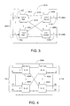
- FIG. 2 illustrates the switch matrix of the present invention.
- a satellite using switch matrix 200 of the present invention uses multiple uplink beams 114 that use c-cell frequency reuse, where c is the number of cells in the reuse pattern.
- Input signals 202A are therefore input to input switch module 204A, and input signals 202A comprise c uplink beams, which equals one entire reuse pattern.
- C is typically equal to 3, 4, 7, 9, or 12, but can be other numbers.
- N is the number of reuse patterns on the ground.
- the total number of uplink beams 114 is c times n (c*n).
- n input switch modules 204A-204N are used to receive all of the c*n uplink beams 114.
- the uplink signals 114 arc multicarrier, and to accomplish the demodulation, the uplink signal 114 is divided into d subbands. Therefore, each input switch module 204A-204N must provide d outputs.
- the output switch modules 206A-206D must accept one input from each input switch module 204A-204N, and therefore have n inputs.
- a demodulator 108 can demodulate one of these d subbands, and m demodulators are devoted to each subband. The total number of demodulators 108 is therefore d*m, and each output switch module 206A-206D must provide m output signals. Therefore, each output switch module is an n*m matrix.
- Switch matrix 200 of the present invention comprises n input switch modules 204A-204N, and d output switch modules 206A-206D.
- Each of the inputs 202A to the input switch module 204A comes from a single uplink reuse group, so that none of the inputs 202A can share an uplink frequency.
- the switch matrix 200 of the present invention thus has a c*m input capability, and a d*m output capability, which provides proper interconnectivity for the system 100 without excess weight or power consumption.
- FIG. 3 illustrates the structure of the input switch modules of the present invention.
- Each input switch module 204A-204N receives inputs 202A-202N.
- input switch module 204A is shown as a typical design.
- Signals 202A which comprise signals 300 and 302, are fed into a plurality, i.e., "c" 1-to-d power splitters 304A-304C
- Each power splitter 304A-304C takes a single input signal, e.g., 300, and produces a plurality of substantially equivalent power outputs from signal 300, e.g., 306A-306D.
- power splitter 304A was a 1:4 power splitter, and a 100 microwatt ( ⁇ W) input signal 300 was fed into power splitter 304A, then power splitter 304A would produce four output signals 306A-306D, each approximately a 25 ⁇ W signal. There would be some losses through power splitter 306A, which would reduce the 25mW output power of each signal by some percentage amount. In the related art, a similar input signal would be split 256 times, making each output signal less than 1 ⁇ W, which may be difficult to process without amplification.
- Each output 306A-306D from each power splitter 304A-304C is fed into a c:1 switch 308A-308D. Since each switch 308A-308D produces only one output 310A-310D, there are d switches 308A-308D in each module 204.
- FIG. 4 illustrates an exemplary output switch module in accordance with the present invention.
- Output switch module 206A shown as a typical output switch module 206, is a concentrator, e.g., output switch module 206A receives the n input signals 310 from the input modules 204 and allows only m of the n input signals 310 to be output signals 116 from output switch module 206A. Every output 116 of an output switch module 206A is connected to a demodulator 108 that demodulates one of the d subbands.
- each output 116 is identical, the output switch module 206A does not have to be fully connected as in the related art, but the output switch module 206A should ensure that in any arrangement of inputs 310, the subset of inputs 310 must be switchable to an output 116. Since each group of c cells cannot use more than d demodulators, m, which is the number of demodulators of one type, must be less than or equal to n, the number of frequency reuse groups.
- the output module 206 Since all of the outputs of the output module 206 are identical, the output module does not have to be fully connected, which allows the present invention to implement a switching scheme that is simpler than a crossbar architecture for the output module 206.
- the output switch module 206A as shown is fully connected, which allows for any traffic pattern on the ground that is supported by frequency reuse rules and by the capacity of the processor to be supported by the output switch module 206. This way, if the traffic distribution changes during the life of the satellite, the switch matrix can be reconfigured to support the new traffic distribution.
- each output submodule 402A-402H are connected to different types of demodulators with each type demodulating a different subband.
- the output switch module 206 can be used with any payload that has multiple uplink beams with frequency reuse and has some sort of processing, analog or digital, that splits the uplink band into several subbands.
- FIG. 5 illustrates a switch matrix in accordance with the present invention that is used in dual-polarized uplink configurations.
- Satellite systems often use a dual polarized uplink, with some signals transmitted up with right-hand circularly polarized (RHCP) carriers with the others using left-hand circularly polarized (LHCP) carriers.
- RHCP right-hand circularly polarized
- LHCP left-hand circularly polarized
- users in a particular uplink beam are constrained to use only one polarization, so that half of the uplink beams use RHCP and the other half of the uplink beams use LHCP.
- system 500 divides the uplink beams 114 in half.
- One-half of the uplink beams 114 in a reuse group will be LHCP, and are grouped in one input module 502A, while the other input beams are RHCP and are grouped in a separate input module 502B.
- the resultant system 500 has twice the number of input modules 502A-502B as system 200, but each input module 502A-502B has one-half the number of inputs as input modules 204A-204N.
- the maximum capacity of the spacecraft is doubled which means twice the number of demodulators 108 can be employed by the spacecraft.
- m the number of demodulators, may be as large as 2n, the number of reuse patterns on the ground, since every reuse pattern may use both polarizations. Therefore, the output switch modules 504A-504B should contain inputs numbering 2n, and outputs numbering m.
- FIG. 5 illustrates the case where the number of uplink beams 114 is even. However, the number of uplink beams 114 can be an odd number, thereby making exact division by two impossible. If the number of uplink beams 114 is an odd number, the c/2 input beams 506 number (c+1)/2, and the number of inputs 508 to the output switch modules 504A-504B number 2c*n/(c+1).
- FIG. 6 illustrates a switch matrix in accordance with the present invention that is used in dual-polarized uplink configurations with varying polarizations within an uplink beam.
- some satellite systems use polarized uplink beams.
- FIG. 5 illustrated the scenario that described users in a particular uplink beam that are constrained to use only one polarization.
- the scenario of FIG. 5 was limited to a fixed polarization for each uplink beam, but this polarization may change over the life of the satellite.
- FIG. 6 illustrates a switch matrix that can be used in such a scenario.
- System 600 utilizes an input signal 114 from every cell c in the reuse group, but doubles the number of outputs from each input switch module 602A-602N to twice the number of bandwidths, i.e., 2d.
- the number of inputs 604 to each output switch module 606A-606D is increased to twice the number of the reuse patterns on the ground, or 2n.
- the maximum capacity of the spacecraft is doubled, so that the number of demodulators 108, or m, can be as large as 2n.
- each input switch module 602 has two outputs 608A-608D that are coupled to an output switch module 606A-606D, e.g., input switch module 602A has two outputs 608A coupled to inputs 604 numbers 1 and 2 on output switch module 606A.
- System 600 can also be used to provide redundancy within the system, for example, if output 1 of input switch module 602A were to fail, output 2 can still connect input switch module 602A to output switch module 606A.
- FIG. 7 illustrates a switch matrix in accordance with the present invention that can use multiple polarizations simultaneously.
- System 700 illustrates a system that uses an uplink antenna with two output ports per beam, one for each polarization. This use of two output ports doubles the number of antenna outputs, which doubles the number of inputs 114 to the number of inputs to the switch matrix 700.
- the number of input switch modules 702A-702N has doubled to 2n, one input switch module 702A-702N for each cell group. As with FIGS.
- the maximum capacity of the spacecraft is doubled since both polarizations are used, and therefore, the number of demodulators may be as large as twice the number of cell patterns on the ground, which forces the number of inputs to the output switch modules 704A-704D to be 2n and the number of outputs to be m, where m may be as large as 2n.
- FIGS. 2-7 are all somewhat vulnerable to single point failures.
- redundancy can be designed into a switch matrix of the present invention to avoid single point failures within the spacecraft. For example, if a switch on an output port of an output module 206A fails, the demodulator 108 that follows the switch is no longer useable, because the demodulator 108 will no longer receive an input. For this reason, additional demodulators 108 in each subband can be installed to allow a signal to be rerouted through the switch matrix of the present invention for that subband.
- the present invention can also have redundancy built in to avoid single point failures within the matrix itself.
- FIG. 2 there are n*d interconnections between the input switch modules 204A-204N and the output switch modules 206A-206D. Since there are only m*d outputs 116, and m ⁇ n, some of the interconnections between input switch modules 204A-204N and output switch modules 206A-206D have no usable signals going through them. If some of the switches are lost on either side of these interconnections, which would render those switches unusable, the impact to the system is typically not very large.
- the loss of an input port to the switch matrix is very serious.
- the uplink beam 114 connected to that port is also unusable. This leads to a hole in the coverage of the satellite where terminals can not uplink to the satellite.
- the input port is connected to a 1:c power splitter, and this passive device typically does not fail nearly as much as an active switch, the small chance of failure is often unacceptable. In these cases, the input module can be redesigned to make it more redundant.
- FIG. 8 illustrates a single input module with redundant input connections in accordance with the present invention.
- the input to the switch matrix includes a downconverter 104 as shown in FIG. 1.
- the input redundancy for the switch matrix can be combined with the downconverter 104 redundancy.
- uplink cells 112 instead of being input directly into downconverters 104, are input to a redundancy matrix 800.
- Redundancy matrix can be used to supply any level of redundancy, but for ease of explanation, a c+1 for c redundancy is described herein. For example, since there are c cells in a reuse group, one additional output is provided from each redundancy matrix 800 to prevent a failure of an input port on input switch module 204A from being a single point failure for a given uplink beam 112.
- redundancy matrix 800 a c+n for c matrix
- input switch module 204A a (c+n) x d matrix
- FIG. 9 illustrates another example of a redundant input matrix of the present invention, related to the embodiment of FIG. 5.
- Input beams 112 for a four cell reuse system having a fixed polarization per cell will use 4 inputs to redundancy matrix 801, which provides an eight-for-seven redundancy.
- Redundancy matrix 801 will produce eight outputs for a single polarization, namely 802A through 802H.
- Each output 802A through 802H is provided to input switch module 204A, and modules 304A through 304D respectively.
- the downconverter 104 redundancy is 8 for 7 as are the inputs to input switch module 204A.
- Redundancy matrix 800 also provides redundancy for each uplink beam 112. If an input to input switch module 204A fails, for example input 802A, uplink beam 112 number 1 can be rerouted to input 802B, which can then switch uplink beam 112 number 1 through input switch module 204A and module 304A. This is done by using hybrid power splitter 900 and hybrid power splitter 902, which can route the uplink beam 112 to either input 802A or 802B. Similar results can be achieved for all of the uplink beams 112.
- uplink beams 112 2, 3, and 4 should all have the same polarization assignment, and uplink beam 112 number 3 should originate from a cell that cannot share frequencies with uplink beam number 2 or uplink beam 112 number 4.
- all of the uplink beams 112 assigned to the redundancy matrix 800 should have the same polarization assignments, and uplink beams 112 assigned to adjacent inputs should originate from cells that cannot share frequencies because they are in the same cell frequency reuse pattern.
- FIG. 9 provides some redundancy in the downconverters 104 and input switch module 204A inputs, the design of FIG. 9 does not allow for two downconverters 104 in a single redundancy matrix 800 to fail, nor does it provide provide any redundancy for the input modules 304A-304D of the input switch module 204A.
- FIG. 10 illustrates a design that provides redundancy in the downconverters and in the input switch module of the present invention.
- System 1000 comprises two redundancy matrices 800. Within each redundancy matrix 800, each uplink beam 112 is input to a hybrid power splitter 900, which has outputs to two different downconverters 104. This configuration makes downconverters 104 fully 2 for 1 redundant, so that more than one downconverter can fail in a single redundancy matrix 800.
- Each uplink beam 112 is also sent to two different power splitter modules 304A-304H within input switch module 204A.
- the primary output for uplink beam 112 1002 is sent to an input on module 304A
- the redundant output for uplink beam 112 1004 is sent to an input on a different module 304B.
- the input switch module 204A can survive the failure of 1 input module 304A-304H.
- uplink beams 112 should be paired such that adjacent inputs should come from cells that have the same polarization assignment and are within the cell frequency reuse pattern.
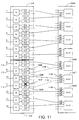
- FIGS. 11 and 12 illustrate examples of failures within the configuration of FIG. 10.
- the downconverter 104P the primary downconverter 104 for uplink beam 112 number 11 has failed.
- the spacecraft either through autonomous operation, monitoring of the downconverter 104P, or manual intervention, can switch to redundant downconverter 104R.
- Input 1100 to module 304G will no longer receive inputs from downconverter 104P.
- uplink beam 112 number 11 can still be switched through input switch module 204A through input 1102 to module 304F.
- Other uplink beams 112 may also have to be switched through the input switch module 204A to prevent interference.
- uplink beam 112 number 9 is typically not within a four cell reuse pattern with uplink beam 112 number 11, so uplink beam 112 number 9 is is also switched to the redundant downconverter 104R associated with uplink beam 112 number 9.
- Input 1104 no longer receives input from uplink beam 112 number 9, which is switched through input switch module 204A through input 1105 on module 304E, and is paired with uplink beam 112 number 8.
- uplink beam 112 number 9 can continue on input 1104 through primary downconverter 104P until primary downconverter 104P fails, or the traffic in the region becomes heavy enough that uplink beam 112 number 9 and uplink beam 112 number 11 must use the same subband.
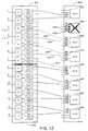
- FIG. 12 illustrates an example where a module 304 in input switch module 204A fails. If module 304B fails, all of the inputs to module 304B become unusable by input switch module 204A.
- the primary inputs 1200 and 1202 are associated with uplink beam 112 number 3 and uplink beam 112 number 4, which must be switched to redundant inputs 1204 and 1206, respectively.
- uplink beams 112 numbers 5, 6, and 7 may also require switching to inputs 1208-1212 respectively to maintain proper pairing or traffic density. If the traffic density is low enough, some of the uplink beams 112 numbers 5, 6, and 7 may be kept with the associated primary downconverter 104, but whenever there are three active inputs on a single module 304 the ability of the payload to concentrate capacity on the associated cells may be impaired.
- FIG. 13 illustrates a complete design of a switch matrix of the present invention.
- the system 1300 of FIG. 13 can be employed.
- the design uses a total of 112 uplink cells, so there are 112 uplink beams 112 going into the downconverters 104.
- the downconverters 104 are 2 for 1 redundant, and the primary and redundant downconverters 104 have separate connections to the switch matrix, for a total of 224 connections.
- the input modules 304 have four inputs and eight outputs, and are connected to the downconverters 104 as shown in FIG. 10.
- the uplink bandwidth is broken into eight subbands, so there are eight different types of demodulators 108. There are thirty-two demodulators 108 used for each subband, although a smaller number, for example twenty-eight demodulators 108, are typically needed to meet capacity specifications. The extra four demodulators 108 in each subband can be used for redundancy.
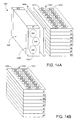
- FIGS. 14A-14B illustrate the packaging of the present invention compared to the related art.
- FIG. 14A illustrates a packaging scheme for the switch matrix of the present invention.
- Switch matrix 1400 consists of an input matrix 1402, an interface plate 1404, and an output matrix 1406.
- the input matrix has a number of "slices” 1408, each containing input modules 1410.
- Output matrix 1406 contains interconnect matrices 1412 and output modules 1414, and consists of a plurality of "slices” each containing interconnect matrices 1412 and output modules 1414.
- the input modules 1410 are connected to interconnect matrices 1412 through the interface plate 1404. As such, there are a large number of signals that must pass through interface plate 1404 to connect input modules 1410 to interconnect matrices 1412 properly.
- FIG. 14B illustrates an alternative packaging design illustrating a simpler packaging design for switch matrix 1416 of the present invention.
- Switch matrix 1416 comprises input modules 1408 directly coupled to output modules 1414, without the need for interface plate 1404 or interconnect matrices 1412. This reduces the signal density, and therefore the complexity of switch matrix 1416, making switch matrix 1416 of the present invention easier to manufacture, test, and integrate into the spacecraft.
- switch matrix 1416 is not a fully connected matrix as the packaging design of FIG. 14A is.
- the switch matrix 1416 is thus less capable of in-flight redistribution of signals, because the beams are grouped into specific sections, and cannot be switched between one section and another.
- many applications may not require a fully connected matrix, and therefore, the packaging of FIG. 14B can be used to simplify the manufacture, testing, and integration of switch matrix 1416 into the spacecraft.
- FIG. 15 is a flow chart illustrating the steps used to practice the present invention.
- Block 1500 illustrates performing the step of grouping the uplink signals into a plurality of groups, the number of groups at least equal to a number of cells in the cell-based transmission matrix, each group comprising a signal from each frequency used in the frequency reuse pattern.
- Block 1502 illustrates performing the step of separating each group of uplink signals into subband signals.
- Block 1504 illustrates performing the step of grouping similar subband signals from the groups of uplink signals to produce groups of similar subband signals.
- Block 1506 illustrates performing the step of forwarding the groups of similar subband signals to demodulators for processing within the satellite system.
- the present invention although described with respect to RF and electrical systems, can also be used with optical systems to accomplish the same goals.
- the switches in the switch matrix can be actual switches, or hybrid electronics, or other switching mechanisms that perform similar functions.
- the present invention discloses a method and apparatus for switching signals through a switch matrix.
- the apparatus comprises an input module and an output module.
- the input module has a plurality of inputs typically equal to a number of cells in a reuse pattern, and the inputs receiving at least one uplink beam
- the input module also has a plurality of outputs, the plurality of outputs is typically equal to the number of subbands in the uplink beam.
- the output module is coupled to the input module and selectively couples the outputs from the input module to an output of the output module.
- the method comprises the steps of grouping the uplink signals into a plurality of groups, the number of groups typically equal to a number of cells in the cell-based transmission matrix, where each group comprises a signal from each frequency used in the frequency reuse pattern.
- Each group of uplink signals is then separated into subband signals, which are then grouped together into groups of similar subband signals.
- the groups of similar subband signals are then forwarded to demodulators for processing within the satellite system.
Abstract
Description
- This invention relates in general to switch matrices, and in particular to a switch matrix for satellite payloads with multiple uplink beams and on-board signal processing.
- Communications satellites have become commonplace for use in many types of communications services, e.g., data transfer, voice communications, television spot beam coverage, and other data transfer applications. As such, satellites must provide signals to various geographic locations on the Earth's surface. As such, typical satellites use customized antenna designs to provide signal coverage for a particular country or geographic area.
- Many satellite payloads contain analog or digital signal processors. Analog processors are typically used to separate and combine different signals into specific channels ("channelize the signals"), and to switch different parts of the ground-to-satellite ("uplink") signal to different satellite-to-ground ("downlink") beams. Digital processors are also used to channelize and switch signals, and may also be used to demodulate, process and remodulate signals. Usually these signal processors are heavy and consume a lot of DC power, so it is advantageous to be as efficient as possible in allocating processing resources to uplink beams.
- Typically, the signals ("traffic") in each uplink beam to the satellite are different, since the population and economy in each uplink region is different. If the amount of traffic in each uplink beam is known before the satellite is launched, and does not vary over the life of the satellite, processing resources can be allocated to uplink beams with fixed connections, which eliminates the need for the switch matrix. Typically, however, the amount of traffic in each uplink beam is either unknown beforehand or varies over time, and thus there must be some sort of switch matrix to reallocate and interconnect uplink beams to the on-board satellite processing resources.
- Some traditional switch matrix designs, such as the crossbar switch or the Clos switch matrix, were designed for use in telephone switching networks, and are designed for point-to-point connectivity. Other switch matrices have been designed for connections inside a computer or between networked computers. Some of these designs are not suitable for satellite signals at microwave frequencies, because the related art switch matrix designs suffer from isolation problems at microwave frequencies. Other switch matrices do not provide for point-to-multipoint connectivity without excessive signal losses caused by power splitting. Many designs are also difficult to build out of smaller pieces in a modular manner.
- It can be seen, then, that there is a need in the art for a switch matrix that is suitable for use in a spacecraft environment. It can also be seen that there is a need in the art for a switch matrix that provides point-to-multipoint connectivity without excessive signal losses. It can also be seen that there is a need in the art for a switch matrix that provides ease of mechanical design and construction to reduce spacecraft costs.
- To overcome the limitations in the prior art described above, and to overcome other limitations that will become apparent upon reading and understanding the present specification, the present invention discloses a method and apparatus for switching signals through a switch matrix. The apparatus comprises an input module and an output module. The input module has a plurality of inputs typically equal to a number of cells in a reuse pattern, and the inputs receiving at least one uplink beam. The input module also has a plurality of outputs, the plurality of outputs is typically equal to the number of subbands in the uplink beam. The output module is coupled to the input module and selectively couples the outputs from the input module to an output of the output module.
- The method comprises the steps of grouping the uplink signals into a plurality of groups, the number of uplink signals typically equal to the number of cells in a cell-based transmission matrix and the number of groups typically equal to a number of cells in a reuse pattern in the cell-based transmission matrix, where each group comprises a signal from each frequency used in the frequency reuse pattern. Each group of uplink signals is then separated into subband signals, which are then grouped together into groups of similar subband signals. The groups of similar subband signals are then forwarded to demodulators for processing within the satellite system.
- The present invention provides a switch matrix that is suitable for use in a spacecraft environment. The present invention also provides a switch matrix that provides point-to-multipoint connectivity without excessive signal losses. The present invention also provides a switch matrix that provides ease of mechanical design and construction to reduce spacecraft costs.
- Referring now to the drawings in which like reference numbers represent corresponding parts throughout:
- FIG. 1 illustrates an exemplary block diagram of the uplink of a satellite with digital processing;
- FIG. 2 illustrates the switch matrix of the present invention;
- FIG. 3 illustrates the structure of the input switch modules of the present invention;
- FIG. 4 illustrates an output switch module in accordance with the present invention;
- FIG. 5 illustrates a switch matrix in accordance with the present invention that is used in dual-polarized uplink configurations;
- FIG. 6 illustrates a switch matrix in accordance with the present invention that is used in dual-polarized uplink configurations with varying polarizations within an uplink beam;
- FIG. 7 illustrates a switch matrix in accordance with the present invention that can use multiple polarizations simultaneously;
- FIG. 8 illustrates a single input module with redundant input connections in accordance with the present invention;
- FIG. 9 illustrates a specific example of a redundant input matrix of the present invention;
- FIG. 10 illustrates a design that provides redundancy in the downconverters and in the input switch module of the present invention;
- FIGS. 11 and 12 illustrate examples of failures within the configuration of FIG. 10;
- FIG. 13 illustrates a complete design of a switch matrix of the present invention;
- FIGS. 14A-14B illustrate the packaging of the present invention compared to the related art; and
- FIG. 15 is a flowchart illustrating the steps used to practice the present invention.
-
- In the following description of the preferred embodiment, reference is made to the accompanying drawings which form a part hereof, and in which is shown by way of illustration a specific embodiment in which the invention may be practiced. It is to be understood that other embodiments may be utilized and structural changes may be made without departing from the scope of the present invention.
- Switch matrices are commonly used in many satellite telecommunications systems designs to allow for redeployment of signals onboard the satellite. The switch matrix allows an input signal to be routed to any output desired through the use of crossbar switches or other types of switch matrices.
- Some traditional switch matrix designs, such as the crossbar switch or the Clos switch matrix, were designed primarily for telephone switching networks, and are designed for point-to-point connectivity. Other switch matrices were designed for connections inside a computer or between networked computers. Some of these designs are not suitable for microwave signals because of isolation problems, and other matrices do not provide for point-to-multipoint connectivity without excessive losses due to power splitting. Many designs are not easy to build out of smaller pieces in a modular manner.
- The present invention is suitable for microwave work, provides for point-to-multipoint connectivity with a greatly reduced amount of power splitting, and can be constructed from smaller pieces in a modular manner.
- FIG. 1 illustrates an exemplary block diagram of the uplink of a satellite with digital processing.
- The
system 100 comprises anuplink antenna 102,downconverters 104,switch matrix 106,demodulators 108, and a digital signal processor (DSP) 110.Uplink antenna 102 receives a number ofuplink beams 112, in thiscase 128uplink beams 112, which are each fed toindividual downconverters 104. Eachdownconverted uplink signal 114 is input to theswitch matrix 106, which routes each signal to a given output of theswitch matrix 106. The output signals 116 of the switch matrix are fed intodemodulators 108, and then input toDSP 110 for processing. TheDSP 110 has the capacity to service a plurality ofdemodulators 108. - The
system 100 is usually employed in a satellite telecommunications system that receives uplink information from transmitters on the ground. These transmitters are assigned in a "cellular" pattern, where each cell transmits information to the satellite within a given frequency band. Each cell within a frequency reuse group of cells uses a different frequency band, and such groups are repeated throughout the cellular pattern to create a frequency-reuse pattern within the totality of cells in the system. Within each cell, the frequency band is divided into subbands. Each subband comprises individual signals from subscriber units, and each subband can contain zero or more signals. - For example, in FIG. 1, each
demodulator 108 demodulates one of eight uplink subbands. If the traffic is uniform, eachuplink beam 112 will be allocated 2demodulators 108, and eachuplink beam 112 can carry ¼ of its maximum capacity. In such a case, eachuplink beam 112 can be hardwired to twodemodulators 108 directly without usingswitch matrix 106, etc. until all 128uplink beams 112 are connected to demodulators 108. - Typically, however, the traffic is not uniform, and each
uplink beam 112 will carry a different amount of traffic, which makes switch matrix 106 a necessary part ofsystem 100. Further, the traffic distribution changes during the lifetime of the satellite, possibly changing every hour or so.Switch matrix 106 is used to dynamically allocatedemodulators 108 to uplink beams 112. In the example of FIG. 1, aswitch matrix 106 with 128 inputs and 256 outputs is needed. - The most straightforward design for the
switch matrix 106 of FIG. 1 is a crossbar switch in which everyinput 114 can be connected to anyoutput 116 in any order, with each signal passing through one switch in theswitch matrix 106. However, such a largecrossbar switch matrix 106 would require 128*256 = 32,768 switches, and would be very difficult to manufacture in a modular manner from smaller switches. - The number of switches in
switch matrix 106 can be somewhat reduced by using architectures like the Clos architecture, but the resulting matrix would still be difficult to manufacture in a modular manner. Crossbar and Closdesign switch matrices 106 are not suitable for thesystem 100 of FIG. 1, either because they are not suitable for microwave switching networks due to isolation and connectivity problems, or because they cannot satisfy the point-to-multipoint requirements forsystem 100. - To broadcast one
uplink signal 114 tomultiple outputs 116, a power splitter is required inside ofswitch matrix 106. The more theuplink signal 114 is split, the greater the power loss through theswitch matrix 106. In power limited applications such as spacecraft, it is vitally important to reduce this power loss as much as possible to reduce the need for amplifiers within thesystem 100, to reduce both power consumption and weight on board the satellite. - For the
switch matrix 106 described in FIG. 1, oneuplink signal 114 must have the capability to be broadcast to 8 of the 256 outputs 116. This capability is typically provided by using a 1:256 power divider, followed by a switching network, withinswitch matrix 106. For satellite applications, this approach leads to unacceptably high losses within theswitch matrix 106. - However, switch
matrices 106 of the related art were not optimized to take into account howsystem 100 is typically implemented. First, satellite payloads withmultiple uplink beams 112 typically use a frequency reuse scheme such as 4-cell or 7-cell frequency reuse. Adjacent cells within the frequency reuse scheme cannot use the same frequency and, therefore, cannot use the same subbands. This reduces the connectivity requirements of theswitch matrix 106, as described herein with respect to the present invention. Second, thedemodulators 108 may often be grouped bysubband, e.g., somedemodulators 108 demodulate only the first subband,other demodulators 108 only the second subband, etc. Oneinput signal 114 must have the capability to be broadcast to all of thedifferent subband demodulator 108 types, but oneinput signal 114 does not have to be broadcast to more than onedemodulator 108 in a given group of demodulators. As such, the switch matrix of the present invention is further reduced in complexity while still providing the interconnections required forsystem 100. - The invention allows for a flexible allocation of processing resources to uplink beams for satellite payloads with on-board processing, which allows the processor resources to be used more efficiently. This reduction on the complexity of the switch matrix reduces the weight and power required by the processor to accomplish the mission goal. The present invention is simpler than comparable switch matrices and can be constructed from simpler switches allowing it to be used for satellite payloads. The amount of power splitting inside the switch matrix of the present invention is reduced, so it has a lower loss and a lower noise figure than other related art designs.
- This invention applies to all satellites with digital or analog processing of signals that divide multiple uplink signals into several subbands. It is most useful when the uplink traffic distribution varies over time or is not well known before launch.
- FIG. 2 illustrates the switch matrix of the present invention. A satellite using
switch matrix 200 of the present invention usesmultiple uplink beams 114 that use c-cell frequency reuse, where c is the number of cells in the reuse pattern. Input signals 202A are therefore input to inputswitch module 204A, andinput signals 202A comprise c uplink beams, which equals one entire reuse pattern. C is typically equal to 3, 4, 7, 9, or 12, but can be other numbers. N is the number of reuse patterns on the ground. As such, the total number ofuplink beams 114 is c times n (c*n). To accommodate the entire complement ofuplink beams 114, ninput switch modules 204A-204N are used to receive all of the c*n uplink beams 114. - The uplink signals 114 arc multicarrier, and to accomplish the demodulation, the
uplink signal 114 is divided into d subbands. Therefore, eachinput switch module 204A-204N must provide d outputs. Theoutput switch modules 206A-206D must accept one input from eachinput switch module 204A-204N, and therefore have n inputs. Ademodulator 108 can demodulate one of these d subbands, and m demodulators are devoted to each subband. The total number ofdemodulators 108 is therefore d*m, and eachoutput switch module 206A-206D must provide m output signals. Therefore, each output switch module is an n*m matrix. -
Switch matrix 200 of the present invention comprises ninput switch modules 204A-204N, and doutput switch modules 206A-206D. Each of theinputs 202A to theinput switch module 204A comes from a single uplink reuse group, so that none of theinputs 202A can share an uplink frequency. Theswitch matrix 200 of the present invention thus has a c*m input capability, and a d*m output capability, which provides proper interconnectivity for thesystem 100 without excess weight or power consumption. - FIG. 3 illustrates the structure of the input switch modules of the present invention. Each
input switch module 204A-204N receivesinputs 202A-202N. For clarity,input switch module 204A is shown as a typical design.Signals 202A, which comprise signals 300 and 302, are fed into a plurality, i.e., "c" 1-to-d power splitters 304A-304C Eachpower splitter 304A-304C takes a single input signal, e.g., 300, and produces a plurality of substantially equivalent power outputs fromsignal 300, e.g., 306A-306D. For example, ifpower splitter 304A was a 1:4 power splitter, and a 100 microwatt (µW)input signal 300 was fed intopower splitter 304A, thenpower splitter 304A would produce fouroutput signals 306A-306D, each approximately a 25 µW signal. There would be some losses throughpower splitter 306A, which would reduce the 25mW output power of each signal by some percentage amount. In the related art, a similar input signal would be split 256 times, making each output signal less than 1µW, which may be difficult to process without amplification. - Each
output 306A-306D from eachpower splitter 304A-304C is fed into a c:1switch 308A-308D. Since eachswitch 308A-308D produces only oneoutput 310A-310D, there ared switches 308A-308D in each module 204. - FIG. 4 illustrates an exemplary output switch module in accordance with the present invention.
Output switch module 206A, shown as a typicaloutput switch module 206, is a concentrator, e.g.,output switch module 206A receives the n input signals 310 from the input modules 204 and allows only m of the n input signals 310 to be output signals 116 fromoutput switch module 206A. Everyoutput 116 of anoutput switch module 206A is connected to ademodulator 108 that demodulates one of the d subbands. Since eachoutput 116 is identical, theoutput switch module 206A does not have to be fully connected as in the related art, but theoutput switch module 206A should ensure that in any arrangement ofinputs 310, the subset ofinputs 310 must be switchable to anoutput 116. Since each group of c cells cannot use more than d demodulators, m, which is the number of demodulators of one type, must be less than or equal to n, the number of frequency reuse groups. - The complexity of the
output switch modules 206 may vary greatly with n and m. For example, if m = n, then theoutput switch modules 206 become straight connections frominput 310 tooutput 116 with no switching required. However, If n is the square of a number, it is possible to build the output module from simpler submodules. As an example shown in FIG. 4, if input signals 310number 64 and the output signals 116number 32, it is possible to build theoutput switch module 206 using eight 8 x 8input submodules 400A-400H and eight 8 x 4output submodules 402A-402H. Since all of the outputs of theoutput module 206 are identical, the output module does not have to be fully connected, which allows the present invention to implement a switching scheme that is simpler than a crossbar architecture for theoutput module 206. However, theoutput switch module 206A as shown is fully connected, which allows for any traffic pattern on the ground that is supported by frequency reuse rules and by the capacity of the processor to be supported by theoutput switch module 206. This way, if the traffic distribution changes during the life of the satellite, the switch matrix can be reconfigured to support the new traffic distribution. - Constructing the
output switch matrix 206 out of simpler submodules 400 and 402 makes it easier to manufacture and test the design of the present invention over that of a full crossbar switch. Modules can be produced and tested separately from the rest, and the production of numerous identical modules can make product design easier. - In the discussion above, it is assumed that the outputs of each
output submodule 402A-402H are connected to different types of demodulators with each type demodulating a different subband. Theoutput switch module 206, however, can be used with any payload that has multiple uplink beams with frequency reuse and has some sort of processing, analog or digital, that splits the uplink band into several subbands. - FIG. 5 illustrates a switch matrix in accordance with the present invention that is used in dual-polarized uplink configurations. Satellite systems often use a dual polarized uplink, with some signals transmitted up with right-hand circularly polarized (RHCP) carriers with the others using left-hand circularly polarized (LHCP) carriers. In some systems, users in a particular uplink beam are constrained to use only one polarization, so that half of the uplink beams use RHCP and the other half of the uplink beams use LHCP.
- As shown in FIG. 5,
system 500 divides the uplink beams 114 in half. One-half of the uplink beams 114 in a reuse group will be LHCP, and are grouped in oneinput module 502A, while the other input beams are RHCP and are grouped in aseparate input module 502B. Theresultant system 500 has twice the number ofinput modules 502A-502B assystem 200, but eachinput module 502A-502B has one-half the number of inputs asinput modules 204A-204N. - Since both polarizations are used in
system 500, the maximum capacity of the spacecraft is doubled which means twice the number ofdemodulators 108 can be employed by the spacecraft. As such, m, the number of demodulators, may be as large as 2n, the number of reuse patterns on the ground, since every reuse pattern may use both polarizations. Therefore, theoutput switch modules 504A-504B should contain inputs numbering 2n, and outputs numbering m. - FIG. 5 illustrates the case where the number of
uplink beams 114 is even. However, the number ofuplink beams 114 can be an odd number, thereby making exact division by two impossible. If the number ofuplink beams 114 is an odd number, the c/2 input beams 506 number (c+1)/2, and the number of inputs 508 to theoutput switch modules 504A-504B number 2c*n/(c+1). - FIG. 6 illustrates a switch matrix in accordance with the present invention that is used in dual-polarized uplink configurations with varying polarizations within an uplink beam. As discuss with respect to FIG. 5, some satellite systems use polarized uplink beams. FIG. 5 illustrated the scenario that described users in a particular uplink beam that are constrained to use only one polarization. The scenario of FIG. 5 was limited to a fixed polarization for each uplink beam, but this polarization may change over the life of the satellite. FIG. 6 illustrates a switch matrix that can be used in such a scenario.
-
System 600 utilizes aninput signal 114 from every cell c in the reuse group, but doubles the number of outputs from eachinput switch module 602A-602N to twice the number of bandwidths, i.e., 2d. To accommodate the increased number of outputs frominput switch modules 602A-602N, the number ofinputs 604 to eachoutput switch module 606A-606D is increased to twice the number of the reuse patterns on the ground, or 2n. As with FIG. 5, since both polarizations are used, the maximum capacity of the spacecraft is doubled, so that the number ofdemodulators 108, or m, can be as large as 2n. However, insystem 600, each input switch module 602 has twooutputs 608A-608D that are coupled to anoutput switch module 606A-606D, e.g.,input switch module 602A has twooutputs 608A coupled toinputs 604numbers output switch module 606A.System 600 can also be used to provide redundancy within the system, for example, ifoutput 1 ofinput switch module 602A were to fail,output 2 can still connectinput switch module 602A tooutput switch module 606A. - FIG. 7 illustrates a switch matrix in accordance with the present invention that can use multiple polarizations simultaneously.
System 700 illustrates a system that uses an uplink antenna with two output ports per beam, one for each polarization. This use of two output ports doubles the number of antenna outputs, which doubles the number ofinputs 114 to the number of inputs to theswitch matrix 700. The number ofinput switch modules 702A-702N has doubled to 2n, oneinput switch module 702A-702N for each cell group. As with FIGS. 5 and 6, the maximum capacity of the spacecraft is doubled since both polarizations are used, and therefore, the number of demodulators may be as large as twice the number of cell patterns on the ground, which forces the number of inputs to theoutput switch modules 704A-704D to be 2n and the number of outputs to be m, where m may be as large as 2n. - The designs of FIGS. 2-7 are all somewhat vulnerable to single point failures. However, redundancy can be designed into a switch matrix of the present invention to avoid single point failures within the spacecraft. For example, if a switch on an output port of an
output module 206A fails, thedemodulator 108 that follows the switch is no longer useable, because thedemodulator 108 will no longer receive an input. For this reason,additional demodulators 108 in each subband can be installed to allow a signal to be rerouted through the switch matrix of the present invention for that subband. - The present invention can also have redundancy built in to avoid single point failures within the matrix itself. For example, referrring to FIG. 2, there are n*d interconnections between the
input switch modules 204A-204N and theoutput switch modules 206A-206D. Since there are only m*d outputs 116, and m<n, some of the interconnections betweeninput switch modules 204A-204N andoutput switch modules 206A-206D have no usable signals going through them. If some of the switches are lost on either side of these interconnections, which would render those switches unusable, the impact to the system is typically not very large. - On the other hand, the loss of an input port to the switch matrix is very serious. Referring again to FIG. 2, if one of the input ports receiving
uplink beams 114 is not useable, theuplink beam 114 connected to that port is also unusable. This leads to a hole in the coverage of the satellite where terminals can not uplink to the satellite. Although the input port is connected to a 1:c power splitter, and this passive device typically does not fail nearly as much as an active switch, the small chance of failure is often unacceptable. In these cases, the input module can be redesigned to make it more redundant. - FIG. 8 illustrates a single input module with redundant input connections in accordance with the present invention.
- Typically, the input to the switch matrix includes a
downconverter 104 as shown in FIG. 1. The input redundancy for the switch matrix can be combined with thedownconverter 104 redundancy. For example,uplink cells 112, instead of being input directly intodownconverters 104, are input to aredundancy matrix 800. Redundancy matrix can be used to supply any level of redundancy, but for ease of explanation, a c+1 for c redundancy is described herein. For example, since there are c cells in a reuse group, one additional output is provided from eachredundancy matrix 800 to prevent a failure of an input port oninput switch module 204A from being a single point failure for a givenuplink beam 112. This providesinputs 802A to 802N to inputswitch module 204A, which is now a (c+1) x d matrix. It can be seen that additional redundancy or alternative redundancy schemes can be provided by making redundancy matrix 800 a c+n for c matrix, and input switch module a (c+n) x d matrix. - FIG. 9 illustrates another example of a redundant input matrix of the present invention, related to the embodiment of FIG. 5. Input beams 112 for a four cell reuse system having a fixed polarization per cell will use 4 inputs to
redundancy matrix 801, which provides an eight-for-seven redundancy.Redundancy matrix 801 will produce eight outputs for a single polarization, namely 802A through 802H. Eachoutput 802A through 802H is provided to inputswitch module 204A, andmodules 304A through 304D respectively. There are a total of eight subbands, and thereforemodules 304A through 304D produce 8 outputs. Thedownconverter 104 redundancy is 8 for 7 as are the inputs to inputswitch module 204A. -
Redundancy matrix 800 also provides redundancy for eachuplink beam 112. If an input to inputswitch module 204A fails, forexample input 802A,uplink beam 112number 1 can be rerouted to input 802B, which can then switchuplink beam 112number 1 throughinput switch module 204A andmodule 304A. This is done by usinghybrid power splitter 900 andhybrid power splitter 902, which can route theuplink beam 112 to eitherinput - Depending on how the
downconverters 104 arc configured, the signal fromuplink beam 112number 3 can be paired with the signal fromuplink beam 112number 2 or the signal fromuplink beam number 4. Therefore, uplink beams 112 2, 3, and 4 should all have the same polarization assignment, anduplink beam 112number 3 should originate from a cell that cannot share frequencies withuplink beam number 2 oruplink beam 112number 4. Preferably, all of the uplink beams 112 assigned to theredundancy matrix 800 should have the same polarization assignments, anduplink beams 112 assigned to adjacent inputs should originate from cells that cannot share frequencies because they are in the same cell frequency reuse pattern. - While the design in FIG. 9 provides some redundancy in the
downconverters 104 andinput switch module 204A inputs, the design of FIG. 9 does not allow for twodownconverters 104 in asingle redundancy matrix 800 to fail, nor does it provide provide any redundancy for theinput modules 304A-304D of theinput switch module 204A. - FIG. 10 illustrates a design that provides redundancy in the downconverters and in the input switch module of the present invention.
-
System 1000 comprises tworedundancy matrices 800. Within eachredundancy matrix 800, eachuplink beam 112 is input to ahybrid power splitter 900, which has outputs to twodifferent downconverters 104. This configuration makesdownconverters 104 fully 2 for 1 redundant, so that more than one downconverter can fail in asingle redundancy matrix 800. - Each
uplink beam 112 is also sent to two differentpower splitter modules 304A-304H withininput switch module 204A. For example the primary output foruplink beam 112 1002 is sent to an input onmodule 304A, while the redundant output foruplink beam 112 1004 is sent to an input on adifferent module 304B. With the configuration of FIG. 10, theinput switch module 204A can survive the failure of 1input module 304A-304H. As with FIG. 9, uplink beams 112 should be paired such that adjacent inputs should come from cells that have the same polarization assignment and are within the cell frequency reuse pattern. - FIGS. 11 and 12 illustrate examples of failures within the configuration of FIG. 10. As shown in FIG. 11, the
downconverter 104P, theprimary downconverter 104 foruplink beam 112number 11 has failed. The spacecraft, either through autonomous operation, monitoring of thedownconverter 104P, or manual intervention, can switch toredundant downconverter 104R.Input 1100 tomodule 304G will no longer receive inputs fromdownconverter 104P. However,uplink beam 112number 11 can still be switched throughinput switch module 204A throughinput 1102 tomodule 304F.Other uplink beams 112 may also have to be switched through theinput switch module 204A to prevent interference. For example,uplink beam 112number 9 is typically not within a four cell reuse pattern withuplink beam 112number 11, souplink beam 112number 9 is is also switched to theredundant downconverter 104R associated withuplink beam 112number 9.Input 1104 no longer receives input fromuplink beam 112number 9, which is switched throughinput switch module 204A through input 1105 onmodule 304E, and is paired withuplink beam 112number 8. If the traffic density is low and if there is no need foruplink beam 112number 9 to use the same subband asuplink beam 112number 11,uplink beam 112number 9 can continue oninput 1104 throughprimary downconverter 104P untilprimary downconverter 104P fails, or the traffic in the region becomes heavy enough that uplinkbeam 112number 9 anduplink beam 112number 11 must use the same subband. - FIG. 12 illustrates an example where a module 304 in
input switch module 204A fails. Ifmodule 304B fails, all of the inputs tomodule 304B become unusable byinput switch module 204A. Theprimary inputs uplink beam 112number 3 anduplink beam 112number 4, which must be switched toredundant inputs - Other switching may have to take place within
input switch module 204A to maintaincorrect uplink beam 112 pairings. For example, uplink beams 112numbers numbers primary downconverter 104, but whenever there are three active inputs on a single module 304 the ability of the payload to concentrate capacity on the associated cells may be impaired. - FIG. 13 illustrates a complete design of a switch matrix of the present invention. For a four-cell reuse pattern with two polarizations, where each cell uses only one of the polarizations, the system 1300 of FIG. 13 can be employed. The design uses a total of 112 uplink cells, so there are 112
uplink beams 112 going into thedownconverters 104. Thedownconverters 104 are 2 for 1 redundant, and the primary andredundant downconverters 104 have separate connections to the switch matrix, for a total of 224 connections. The input modules 304 have four inputs and eight outputs, and are connected to thedownconverters 104 as shown in FIG. 10. The uplink bandwidth is broken into eight subbands, so there are eight different types ofdemodulators 108. There are thirty-twodemodulators 108 used for each subband, although a smaller number, for example twenty-eightdemodulators 108, are typically needed to meet capacity specifications. The extra fourdemodulators 108 in each subband can be used for redundancy. - FIGS. 14A-14B illustrate the packaging of the present invention compared to the related art.
- FIG. 14A illustrates a packaging scheme for the switch matrix of the present invention.
Switch matrix 1400 consists of aninput matrix 1402, aninterface plate 1404, and anoutput matrix 1406. The input matrix has a number of "slices" 1408, each containinginput modules 1410.Output matrix 1406 containsinterconnect matrices 1412 andoutput modules 1414, and consists of a plurality of "slices" each containinginterconnect matrices 1412 andoutput modules 1414. Theinput modules 1410 are connected to interconnectmatrices 1412 through theinterface plate 1404. As such, there are a large number of signals that must pass throughinterface plate 1404 to connectinput modules 1410 to interconnectmatrices 1412 properly. - FIG. 14B illustrates an alternative packaging design illustrating a simpler packaging design for
switch matrix 1416 of the present invention.Switch matrix 1416 comprisesinput modules 1408 directly coupled tooutput modules 1414, without the need forinterface plate 1404 orinterconnect matrices 1412. This reduces the signal density, and therefore the complexity ofswitch matrix 1416, makingswitch matrix 1416 of the present invention easier to manufacture, test, and integrate into the spacecraft. However,switch matrix 1416 is not a fully connected matrix as the packaging design of FIG. 14A is. Theswitch matrix 1416 is thus less capable of in-flight redistribution of signals, because the beams are grouped into specific sections, and cannot be switched between one section and another. However, many applications may not require a fully connected matrix, and therefore, the packaging of FIG. 14B can be used to simplify the manufacture, testing, and integration ofswitch matrix 1416 into the spacecraft. - FIG. 15 is a flow chart illustrating the steps used to practice the present invention.
-
Block 1500 illustrates performing the step of grouping the uplink signals into a plurality of groups, the number of groups at least equal to a number of cells in the cell-based transmission matrix, each group comprising a signal from each frequency used in the frequency reuse pattern. -
Block 1502 illustrates performing the step of separating each group of uplink signals into subband signals. -
Block 1504 illustrates performing the step of grouping similar subband signals from the groups of uplink signals to produce groups of similar subband signals. -
Block 1506 illustrates performing the step of forwarding the groups of similar subband signals to demodulators for processing within the satellite system. - This concludes the description of the preferred embodiment of the invention. The following paragraphs describe some alternative methods of accomplishing the same objects. The present invention, although described with respect to RF and electrical systems, can also be used with optical systems to accomplish the same goals. Further, the switches in the switch matrix can be actual switches, or hybrid electronics, or other switching mechanisms that perform similar functions.
- In summary, the present invention discloses a method and apparatus for switching signals through a switch matrix. The apparatus comprises an input module and an output module. The input module has a plurality of inputs typically equal to a number of cells in a reuse pattern, and the inputs receiving at least one uplink beam The input module also has a plurality of outputs, the plurality of outputs is typically equal to the number of subbands in the uplink beam. The output module is coupled to the input module and selectively couples the outputs from the input module to an output of the output module.
- The method comprises the steps of grouping the uplink signals into a plurality of groups, the number of groups typically equal to a number of cells in the cell-based transmission matrix, where each group comprises a signal from each frequency used in the frequency reuse pattern. Each group of uplink signals is then separated into subband signals, which are then grouped together into groups of similar subband signals. The groups of similar subband signals are then forwarded to demodulators for processing within the satellite system.
- The foregoing description of the preferred embodiment of die invention has been presented for the purposes of illustration and description. It is not intended to be exhaustive or to limit the invention to the precise form disclosed. Many modifications and variations are possible in light of the above teaching It is intended that the scope of the invention be limited not by this detailed description, but rather by the claims appended hereto.
Claims (11)
- A switch matrix (200; 500; 600; 700; 1300; 1400; 1416) for coupling an uplink beam (114) to a demodulator (108), characterized by:an input module (204; 502; 602), the input module (204) having a plurality of inputs (202; 506; 802) at least equal to a number (c) of cells in a reuse pattern, the inputs (202; 506; 802) receiving at least one uplink beam, and a plurality of outputs (608), the plurality of outputs (608) at least equal to a number (d) of subbands in the uplink beam; andan output module (206), the output module (206) coupled to the input module (204; 502; 602), for selectively coupling the outputs (608) from the input module (204; 502; 602) to an output (116) of the output module (206), the output (116) of the output module (206) coupled to a demodulator (108) thereto.
- The switch matrix of claim 1, characterized in that the output module (206) is directly coupled to the input module (204).
- The switch matrix of claim 1 or 2, characterized in that the input module (204) comprises redundant modules (800).
- The switch matrix of any of claims 1-3, characterized in that the input module (204) accepts uplink beams of different polarizations.
- The switch matrix of claim 4, characterized in that the input module (204) accepts uplink beams of a single polarization.
- A switch matrix (200; 500; 600; 700; 1300; 1400; 1416) for coupling an uplink beam (114) to a demodulator (108) in a satellite system (100), wherein the satellite system (100) receives input from cells in a cell pattern, comprising:(a) a plurality of input modules (204; 502; 602), each having a plurality of inputs (202; 506; 802) at least equal to a number (c) of cells in a reuse pattern for the satellite system (100), each input module (204) comprising:(1) a plurality of power splitters (304), wherein the plurality of power splitters (304) is at least equal to the number (c) of cells in the reuse pattern for the satellite system (100), wherein each power splitter (304) splits each input into a plurality of substantially equal power outputs (306), a number (d) of power outputs (306) at least equal to a number of subbands used by the satellite system (100); and(2) a plurality of switch modules (308), coupled to the plurality of power splitters (304), each switch module (308) accepting a plurality of inputs at least equal to the number (c) of cells in the reuse pattern for the satellite system (100), the plurality of switch modules (308) at least equal to the number (d) of subbands used by the satellite system (100); and(b) a plurality of output modules (206), coupled to the input modules (204) through the plurality of the switch modules (308), each having a plurality of inputs at least equal to the number (c) of cells in the cell pattern, comprising:(1) a first set of output matrices (400), each output matrix (400) in the first set of output matrices (400) having a plurality of inputs at least equal to the number (d) of subbands used by the satellite system (100); and(2) a second set of output matrices (402), coupled to the first set of output matrices (400), each output matrix (402) in the second set of output matrices having a plurality of outputs at least equal to a number of demodulators used by the satellite system (100) in each subband.
- The switch matrix of claim 6, characterized in that each output module (206) is directly coupled to the input modules (204).
- The switch matrix of claim 6 or 7, characterized in that the input modules (204) comprise redundant modules (800).
- The switch matrix of any of claims 6-8, characterized in that the input modules (204) accept uplink beams of different polarizations.
- The switch matrix of Claim 9, characterized in that the input modules (204) each accept uplink beams of a single polarization.
- A method for switching uplink signals (114) through a switch matrix (200; 500; 600; 700; 1300; 1400; 1416) in a satellite system (100), the uplink signal generated by a cell-based transmission matrix, wherein a frequency reuse pattern is used throughout the cell matrix and the uplink signal (114) comprises subband signals, comprising:grouping (1500) the uplink signals into a plurality of groups, the number of groups at least equal to a number of cell-reuse patterns of the cell-based transmission matrix, each group comprising a signal from each frequency used in the frequency reuse pattern;separating (1502) each group of uplink signals into subband signals;grouping (1504) similar subband signals from the groups of uplink signals to produce groups of similar subband signals; andforwarding (1506) the groups of similar subband signals to demodulators for processing within the satellite system.
Applications Claiming Priority (2)
| Application Number | Priority Date | Filing Date | Title |
|---|---|---|---|
| US09/538,030 US7031653B1 (en) | 2000-03-29 | 2000-03-29 | Switch matrix for satellite payloads with multiple uplink beams and on-board signal processing |
| US538030 | 2000-03-29 |
Publications (3)
| Publication Number | Publication Date |
|---|---|
| EP1139584A2 true EP1139584A2 (en) | 2001-10-04 |
| EP1139584A3 EP1139584A3 (en) | 2004-01-02 |
| EP1139584B1 EP1139584B1 (en) | 2010-09-29 |
Family
ID=24145135
Family Applications (1)
| Application Number | Title | Priority Date | Filing Date |
|---|---|---|---|
| EP01107653A Expired - Lifetime EP1139584B1 (en) | 2000-03-29 | 2001-03-28 | switch matrix for satellite payloads with multiple uplink beams and on-board signal processing |
Country Status (5)
| Country | Link |
|---|---|
| US (1) | US7031653B1 (en) |
| EP (1) | EP1139584B1 (en) |
| JP (1) | JP3839679B2 (en) |
| CA (1) | CA2340488C (en) |
| DE (1) | DE60143142D1 (en) |
Cited By (2)
| Publication number | Priority date | Publication date | Assignee | Title |
|---|---|---|---|---|
| EP1590906A2 (en) * | 2003-01-28 | 2005-11-02 | The Boeing Company | Systems and methods for digital processing of satellite communications data |
| EP2728770A3 (en) * | 2012-11-01 | 2014-07-30 | The Boeing Company | Satellite transponder with a system and a method for processing communication data by analog digital conversion of the signals, formation of frequency channels and combination of them by a switch with a plurality of stages. |
Families Citing this family (12)
| Publication number | Priority date | Publication date | Assignee | Title |
|---|---|---|---|---|
| FR2837043B1 (en) * | 2002-03-05 | 2004-06-04 | Cit Alcatel | SWITCHING SYSTEM, TRANSMISSION DEVICE, TRANSMISSION METHOD AND SWITCHING METHOD FOR SATELLITE |
| US7639646B2 (en) * | 2004-03-17 | 2009-12-29 | Qualcomm Incorporated | Satellite diversity system, apparatus and method |
| US20070125984A1 (en) * | 2005-12-01 | 2007-06-07 | Sarnoff Corporation | Phosphors protected against moisture and LED lighting devices |
| US20080055151A1 (en) * | 2006-08-29 | 2008-03-06 | Wildblue Communications, Inc. | Network-Access Satellite Communication System |
| US8538323B2 (en) * | 2006-09-26 | 2013-09-17 | Viasat, Inc. | Satellite architecture |
| EP2111697B1 (en) * | 2006-09-26 | 2016-09-21 | ViaSat, Inc. | Improved spot beam satellite systems |
| US7792070B1 (en) * | 2007-04-13 | 2010-09-07 | Douglas Burr | Multi-beam satellite network to maximize bandwidth utilization |
| US9236934B1 (en) | 2009-10-16 | 2016-01-12 | Viasat, Inc. | Satellite system architecture for coverage areas of disparate demand |
| FR2952451B1 (en) * | 2009-11-10 | 2011-12-23 | Thales Sa | DYNAMIC MANAGEMENT OF THE FREQUENCY ROUTING CAPABILITY OF A TRANSPARENT DIGITAL PROCESSOR |
| EP2999117B1 (en) * | 2014-09-19 | 2018-05-16 | Nxp B.V. | Device and method for switchably routing down-converted RF signals |
| EP3238090A4 (en) * | 2014-12-24 | 2018-08-08 | Intel Corporation | Apparatus and method for using multiple multi-drop buses |
| US9848370B1 (en) * | 2015-03-16 | 2017-12-19 | Rkf Engineering Solutions Llc | Satellite beamforming |
Citations (3)
| Publication number | Priority date | Publication date | Assignee | Title |
|---|---|---|---|---|
| US5220320A (en) * | 1988-03-11 | 1993-06-15 | Comsat | Switch matrix including both B switching elements and crossbar switch matrices |
| US5790529A (en) * | 1996-08-01 | 1998-08-04 | Motorola, Inc. | Communications network node with switched channelizer architecture |
| EP1075094A2 (en) * | 1999-08-05 | 2001-02-07 | Hughes Electronics Corporation | A scalable switch matrix and demodulator bank architecture for a satellite uplink receiver |
Family Cites Families (12)
| Publication number | Priority date | Publication date | Assignee | Title |
|---|---|---|---|---|
| IT1130545B (en) * | 1980-12-03 | 1986-06-18 | Cselt Centro Studi Lab Telecom | PROCEDURE AND SYSTEM FOR ACCESS TO A SATELLITE FOR TELECOMMUNICATIONS WITH COMMUNICATION ON BOARD |
| US4425639A (en) * | 1981-01-12 | 1984-01-10 | Bell Telephone Laboratories, Incorporated | Satellite communications system with frequency channelized beams |
| US4456988A (en) * | 1981-01-29 | 1984-06-26 | Kokusai Denshin Denwa Kabushiki Kaisha | Satellite repeater |
| US4931802A (en) * | 1988-03-11 | 1990-06-05 | Communications Satellite Corporation | Multiple spot-beam systems for satellite communications |
| US5736959A (en) * | 1991-10-28 | 1998-04-07 | Teledesic Corporation | Earth-fixed cell beam management for satellite communication system using dielectic lens-focused scanning beam antennas |
| US6334219B1 (en) | 1994-09-26 | 2001-12-25 | Adc Telecommunications Inc. | Channel selection for a hybrid fiber coax network |
| KR960027576A (en) * | 1994-12-01 | 1996-07-22 | 리차드 탤런 | Wireless Signal Scanning and Targeting System for Land Mobile Wireless Base Sites |
| US6377561B1 (en) * | 1996-06-24 | 2002-04-23 | Spar Aerospace Limited | Data communication satellite system and method of carrying multi-media traffic |
| US5956620A (en) * | 1997-01-17 | 1999-09-21 | Com Dev Limited | Analog processor for digital satellites |
| US6198435B1 (en) * | 1997-01-27 | 2001-03-06 | Metawave Communications Corporation | System and method for improved trunking efficiency through sector overlap |
| US6259899B1 (en) * | 1998-11-04 | 2001-07-10 | Hughes Electrical Corporation | System and method for analysis of intermodulation dispersion |
| US6643294B1 (en) * | 1999-12-09 | 2003-11-04 | Verizon Laboratories Inc. | Distributed control merged buffer ATM switch |
-
2000
- 2000-03-29 US US09/538,030 patent/US7031653B1/en not_active Expired - Lifetime
-
2001
- 2001-03-13 CA CA002340488A patent/CA2340488C/en not_active Expired - Lifetime
- 2001-03-28 DE DE60143142T patent/DE60143142D1/en not_active Expired - Lifetime
- 2001-03-28 EP EP01107653A patent/EP1139584B1/en not_active Expired - Lifetime
- 2001-03-29 JP JP2001095520A patent/JP3839679B2/en not_active Expired - Lifetime
Patent Citations (3)
| Publication number | Priority date | Publication date | Assignee | Title |
|---|---|---|---|---|
| US5220320A (en) * | 1988-03-11 | 1993-06-15 | Comsat | Switch matrix including both B switching elements and crossbar switch matrices |
| US5790529A (en) * | 1996-08-01 | 1998-08-04 | Motorola, Inc. | Communications network node with switched channelizer architecture |
| EP1075094A2 (en) * | 1999-08-05 | 2001-02-07 | Hughes Electronics Corporation | A scalable switch matrix and demodulator bank architecture for a satellite uplink receiver |
Non-Patent Citations (1)
| Title |
|---|
| MARUYAMA H ET AL: "Onboard processor for millimeter-wave personal satellite communications system" PROCEEDINGS OF THE INTERNATIONAL CONFERENCE ON COMMUNICATIONS (ICC). GENEVA, MAY 23 - 26, 1993, NEW YORK, IEEE, US, vol. 3, 23 May 1993 (1993-05-23), pages 1480-1486, XP010137132 ISBN: 0-7803-0950-2 * |
Cited By (8)
| Publication number | Priority date | Publication date | Assignee | Title |
|---|---|---|---|---|
| EP1590906A2 (en) * | 2003-01-28 | 2005-11-02 | The Boeing Company | Systems and methods for digital processing of satellite communications data |
| EP1590906A4 (en) * | 2003-01-28 | 2009-12-02 | Boeing Co | Systems and methods for digital processing of satellite communications data |
| EP2728770A3 (en) * | 2012-11-01 | 2014-07-30 | The Boeing Company | Satellite transponder with a system and a method for processing communication data by analog digital conversion of the signals, formation of frequency channels and combination of them by a switch with a plurality of stages. |
| EP2728770B1 (en) | 2012-11-01 | 2016-08-03 | The Boeing Company | Satellite transponder with a system and a method for processing communication data by analog digital conversion of the signals, formation of frequency channels and combination of them by a switch with a plurality of stages. |
| EP3091673A3 (en) * | 2012-11-01 | 2016-11-16 | The Boeing Company | Satellite transponder with a system and a method for processing communication data by analog digital conversion of the signals, formation of frequency channels and combination of them by a switch with a plurality of stages. |
| EP3091673B1 (en) | 2012-11-01 | 2018-02-14 | The Boeing Company | Satellite transponder with a system and a method for processing communication data by analog digital conversion of the signals, formation of frequency channels and combination of them by a switch with a plurality of stages. |
| EP3297181A1 (en) * | 2012-11-01 | 2018-03-21 | The Boeing Company | Satellite transponder with a system and a method for processing communication data by analog digital conversion of the signals, formation of frequency channels and combination of them by a switch with a plurality of stages |
| US9954602B2 (en) | 2012-11-01 | 2018-04-24 | The Boeing Company | Satellite communications data processing |
Also Published As
| Publication number | Publication date |
|---|---|
| CA2340488C (en) | 2007-05-22 |
| CA2340488A1 (en) | 2001-09-29 |
| DE60143142D1 (en) | 2010-11-11 |
| US7031653B1 (en) | 2006-04-18 |
| EP1139584B1 (en) | 2010-09-29 |
| JP3839679B2 (en) | 2006-11-01 |
| EP1139584A3 (en) | 2004-01-02 |
| JP2001333006A (en) | 2001-11-30 |
Similar Documents
| Publication | Publication Date | Title |
|---|---|---|
| US4232266A (en) | Technique for sharing a plurality of transponders among a same or larger number of channels | |
| EP1139584B1 (en) | switch matrix for satellite payloads with multiple uplink beams and on-board signal processing | |
| EP0756762B1 (en) | Antenna system | |
| RU2136107C1 (en) | Load of communication satellite, assembly for transmitting phase-locked antenna array, and assembly for receiving phase-locked antenna array | |
| EP0201254B1 (en) | Terrestrial communications system base station | |
| KR950013616B1 (en) | Signal routing system | |
| US8134939B2 (en) | Multichannel ring and star networks with limited channel conversion | |
| SE429280B (en) | MULTI-CHANNEL SENDER SYSTEM FOR A MOBILE COMMUNICATION SYSTEM | |
| EP3576317B1 (en) | Hitless rearrangement of a satellite-hosted switch via propagated synchronization | |
| JP2003249884A (en) | Apparatus and method for implementing flexible hub- spoke satellite communication network | |
| US6539201B2 (en) | Scalable switch matrix and demodulator bank architecture for a satellite uplink receiver | |
| US10284283B2 (en) | Access switch network with redundancy | |
| WO2004103325A1 (en) | Offset satellite communication cell arrays with orthogonal polarizations | |
| US7835733B1 (en) | Satellite telecommunication system | |
| US6515579B1 (en) | Switching apparatus for routing communication channels through a satellite payload | |
| WO2022216410A1 (en) | Techniques for end-to-end beamforming with multiple areas of simultaneous user coverage | |
| JPH07131265A (en) | Multiport amplifier |
Legal Events
| Date | Code | Title | Description |
|---|---|---|---|
| PUAI | Public reference made under article 153(3) epc to a published international application that has entered the european phase |
Free format text: ORIGINAL CODE: 0009012 |
|
| AK | Designated contracting states |
Kind code of ref document: A2 Designated state(s): AT BE CH CY DE DK ES FI FR GB GR IE IT LI LU MC NL PT SE TR |
|
| AX | Request for extension of the european patent |
Free format text: AL;LT;LV;MK;RO;SI |
|
| PUAL | Search report despatched |
Free format text: ORIGINAL CODE: 0009013 |
|
| AK | Designated contracting states |
Kind code of ref document: A3 Designated state(s): AT BE CH CY DE DK ES FI FR GB GR IE IT LI LU MC NL PT SE TR |
|
| AX | Request for extension of the european patent |
Extension state: AL LT LV MK RO SI |
|
| 17P | Request for examination filed |
Effective date: 20040625 |
|
| AKX | Designation fees paid |
Designated state(s): DE FR GB IT |
|
| 17Q | First examination report despatched |
Effective date: 20080121 |
|
| GRAP | Despatch of communication of intention to grant a patent |
Free format text: ORIGINAL CODE: EPIDOSNIGR1 |
|
| GRAS | Grant fee paid |
Free format text: ORIGINAL CODE: EPIDOSNIGR3 |
|
| GRAA | (expected) grant |
Free format text: ORIGINAL CODE: 0009210 |
|
| AK | Designated contracting states |
Kind code of ref document: B1 Designated state(s): DE FR GB IT |
|
| REG | Reference to a national code |
Ref country code: GB Ref legal event code: FG4D |
|
| REF | Corresponds to: |
Ref document number: 60143142 Country of ref document: DE Date of ref document: 20101111 Kind code of ref document: P |
|
| PLBE | No opposition filed within time limit |
Free format text: ORIGINAL CODE: 0009261 |
|
| STAA | Information on the status of an ep patent application or granted ep patent |
Free format text: STATUS: NO OPPOSITION FILED WITHIN TIME LIMIT |
|
| 26N | No opposition filed |
Effective date: 20110630 |
|
| REG | Reference to a national code |
Ref country code: DE Ref legal event code: R097 Ref document number: 60143142 Country of ref document: DE Effective date: 20110630 |
|
| REG | Reference to a national code |
Ref country code: FR Ref legal event code: PLFP Year of fee payment: 16 |
|
| REG | Reference to a national code |
Ref country code: FR Ref legal event code: PLFP Year of fee payment: 17 |
|
| REG | Reference to a national code |
Ref country code: FR Ref legal event code: PLFP Year of fee payment: 18 |
|
| PGFP | Annual fee paid to national office [announced via postgrant information from national office to epo] |
Ref country code: DE Payment date: 20200327 Year of fee payment: 20 Ref country code: GB Payment date: 20200327 Year of fee payment: 20 Ref country code: IT Payment date: 20200323 Year of fee payment: 20 |
|
| PGFP | Annual fee paid to national office [announced via postgrant information from national office to epo] |
Ref country code: FR Payment date: 20200325 Year of fee payment: 20 |
|
| REG | Reference to a national code |
Ref country code: DE Ref legal event code: R071 Ref document number: 60143142 Country of ref document: DE |
|
| REG | Reference to a national code |
Ref country code: GB Ref legal event code: PE20 Expiry date: 20210327 |
|
| PG25 | Lapsed in a contracting state [announced via postgrant information from national office to epo] |
Ref country code: GB Free format text: LAPSE BECAUSE OF EXPIRATION OF PROTECTION Effective date: 20210327 |