EP1148362A1 - Arrayed waveguide grating having a reflective input coupling - Google Patents
Arrayed waveguide grating having a reflective input coupling Download PDFInfo
- Publication number
- EP1148362A1 EP1148362A1 EP01303543A EP01303543A EP1148362A1 EP 1148362 A1 EP1148362 A1 EP 1148362A1 EP 01303543 A EP01303543 A EP 01303543A EP 01303543 A EP01303543 A EP 01303543A EP 1148362 A1 EP1148362 A1 EP 1148362A1
- Authority
- EP
- European Patent Office
- Prior art keywords
- input
- waveguide
- grating
- waveguides
- arrayed
- Prior art date
- Legal status (The legal status is an assumption and is not a legal conclusion. Google has not performed a legal analysis and makes no representation as to the accuracy of the status listed.)
- Withdrawn
Links
Images


Classifications
-
- G—PHYSICS
- G02—OPTICS
- G02B—OPTICAL ELEMENTS, SYSTEMS OR APPARATUS
- G02B6/00—Light guides; Structural details of arrangements comprising light guides and other optical elements, e.g. couplings
- G02B6/10—Light guides; Structural details of arrangements comprising light guides and other optical elements, e.g. couplings of the optical waveguide type
- G02B6/12—Light guides; Structural details of arrangements comprising light guides and other optical elements, e.g. couplings of the optical waveguide type of the integrated circuit kind
- G02B6/12007—Light guides; Structural details of arrangements comprising light guides and other optical elements, e.g. couplings of the optical waveguide type of the integrated circuit kind forming wavelength selective elements, e.g. multiplexer, demultiplexer
- G02B6/12009—Light guides; Structural details of arrangements comprising light guides and other optical elements, e.g. couplings of the optical waveguide type of the integrated circuit kind forming wavelength selective elements, e.g. multiplexer, demultiplexer comprising arrayed waveguide grating [AWG] devices, i.e. with a phased array of waveguides
- G02B6/12016—Light guides; Structural details of arrangements comprising light guides and other optical elements, e.g. couplings of the optical waveguide type of the integrated circuit kind forming wavelength selective elements, e.g. multiplexer, demultiplexer comprising arrayed waveguide grating [AWG] devices, i.e. with a phased array of waveguides characterised by the input or output waveguides, e.g. tapered waveguide ends, coupled together pairs of output waveguides
-
- G—PHYSICS
- G02—OPTICS
- G02B—OPTICAL ELEMENTS, SYSTEMS OR APPARATUS
- G02B6/00—Light guides; Structural details of arrangements comprising light guides and other optical elements, e.g. couplings
- G02B6/10—Light guides; Structural details of arrangements comprising light guides and other optical elements, e.g. couplings of the optical waveguide type
- G02B6/12—Light guides; Structural details of arrangements comprising light guides and other optical elements, e.g. couplings of the optical waveguide type of the integrated circuit kind
- G02B6/12004—Combinations of two or more optical elements
-
- G—PHYSICS
- G02—OPTICS
- G02B—OPTICAL ELEMENTS, SYSTEMS OR APPARATUS
- G02B6/00—Light guides; Structural details of arrangements comprising light guides and other optical elements, e.g. couplings
- G02B6/10—Light guides; Structural details of arrangements comprising light guides and other optical elements, e.g. couplings of the optical waveguide type
- G02B6/12—Light guides; Structural details of arrangements comprising light guides and other optical elements, e.g. couplings of the optical waveguide type of the integrated circuit kind
- G02B6/12007—Light guides; Structural details of arrangements comprising light guides and other optical elements, e.g. couplings of the optical waveguide type of the integrated circuit kind forming wavelength selective elements, e.g. multiplexer, demultiplexer
- G02B6/12009—Light guides; Structural details of arrangements comprising light guides and other optical elements, e.g. couplings of the optical waveguide type of the integrated circuit kind forming wavelength selective elements, e.g. multiplexer, demultiplexer comprising arrayed waveguide grating [AWG] devices, i.e. with a phased array of waveguides
- G02B6/12023—Light guides; Structural details of arrangements comprising light guides and other optical elements, e.g. couplings of the optical waveguide type of the integrated circuit kind forming wavelength selective elements, e.g. multiplexer, demultiplexer comprising arrayed waveguide grating [AWG] devices, i.e. with a phased array of waveguides characterised by means for reducing the polarisation dependence, e.g. reduced birefringence
-
- G—PHYSICS
- G02—OPTICS
- G02B—OPTICAL ELEMENTS, SYSTEMS OR APPARATUS
- G02B6/00—Light guides; Structural details of arrangements comprising light guides and other optical elements, e.g. couplings
- G02B6/10—Light guides; Structural details of arrangements comprising light guides and other optical elements, e.g. couplings of the optical waveguide type
- G02B6/12—Light guides; Structural details of arrangements comprising light guides and other optical elements, e.g. couplings of the optical waveguide type of the integrated circuit kind
- G02B6/12007—Light guides; Structural details of arrangements comprising light guides and other optical elements, e.g. couplings of the optical waveguide type of the integrated circuit kind forming wavelength selective elements, e.g. multiplexer, demultiplexer
- G02B6/12009—Light guides; Structural details of arrangements comprising light guides and other optical elements, e.g. couplings of the optical waveguide type of the integrated circuit kind forming wavelength selective elements, e.g. multiplexer, demultiplexer comprising arrayed waveguide grating [AWG] devices, i.e. with a phased array of waveguides
- G02B6/12026—Light guides; Structural details of arrangements comprising light guides and other optical elements, e.g. couplings of the optical waveguide type of the integrated circuit kind forming wavelength selective elements, e.g. multiplexer, demultiplexer comprising arrayed waveguide grating [AWG] devices, i.e. with a phased array of waveguides characterised by means for reducing the temperature dependence
- G02B6/1203—Light guides; Structural details of arrangements comprising light guides and other optical elements, e.g. couplings of the optical waveguide type of the integrated circuit kind forming wavelength selective elements, e.g. multiplexer, demultiplexer comprising arrayed waveguide grating [AWG] devices, i.e. with a phased array of waveguides characterised by means for reducing the temperature dependence using mounting means, e.g. by using a combination of materials having different thermal expansion coefficients
-
- G—PHYSICS
- G02—OPTICS
- G02B—OPTICAL ELEMENTS, SYSTEMS OR APPARATUS
- G02B6/00—Light guides; Structural details of arrangements comprising light guides and other optical elements, e.g. couplings
- G02B6/24—Coupling light guides
- G02B6/26—Optical coupling means
- G02B6/27—Optical coupling means with polarisation selective and adjusting means
- G02B6/2706—Optical coupling means with polarisation selective and adjusting means as bulk elements, i.e. free space arrangements external to a light guide, e.g. polarising beam splitters
-
- G—PHYSICS
- G02—OPTICS
- G02B—OPTICAL ELEMENTS, SYSTEMS OR APPARATUS
- G02B6/00—Light guides; Structural details of arrangements comprising light guides and other optical elements, e.g. couplings
- G02B6/24—Coupling light guides
- G02B6/26—Optical coupling means
- G02B6/27—Optical coupling means with polarisation selective and adjusting means
- G02B6/2753—Optical coupling means with polarisation selective and adjusting means characterised by their function or use, i.e. of the complete device
- G02B6/2766—Manipulating the plane of polarisation from one input polarisation to another output polarisation, e.g. polarisation rotators, linear to circular polarisation converters
-
- G—PHYSICS
- G02—OPTICS
- G02B—OPTICAL ELEMENTS, SYSTEMS OR APPARATUS
- G02B6/00—Light guides; Structural details of arrangements comprising light guides and other optical elements, e.g. couplings
- G02B6/24—Coupling light guides
- G02B6/26—Optical coupling means
- G02B6/27—Optical coupling means with polarisation selective and adjusting means
- G02B6/2753—Optical coupling means with polarisation selective and adjusting means characterised by their function or use, i.e. of the complete device
- G02B6/2773—Polarisation splitting or combining
Landscapes
- Physics & Mathematics (AREA)
- General Physics & Mathematics (AREA)
- Optics & Photonics (AREA)
- Engineering & Computer Science (AREA)
- Microelectronics & Electronic Packaging (AREA)
- Optical Integrated Circuits (AREA)
- Optical Couplings Of Light Guides (AREA)
- Diffracting Gratings Or Hologram Optical Elements (AREA)
Abstract
Description
- The present invention relates to an arrayed waveguide grating having a reflective input, and particularly a reflective input that permits variable coupling to adjust the center wavelength.
- An arrayed waveguide grating (AWG) is a dispersive optical device used for multiplexing or demultiplexing a set of optical telecommunications channels having different wavelengths. An example of an AWG is shown in Fig. 1. The AWG 100 is an integrated optics device formed on a substrate. The AWG has at least one
input waveguide 10 for launching a multiplexed signal comprising a plurality of wavelength channels, λ1 to λn, into a free-space slab such as astar coupler 12. Thestar coupler 12 distributes a wavefront of the signal evenly to a plurality of waveguides that form thegrating 14. Each of the plurality of waveguides has a different optical length, the optical lengths of adjacent waveguides differing by a constant value and increasing geometrically from one side of the grating to the other. Interference caused by the relative phase differences introduced by thegrating 14 occurs in a second free-space slab such as astar coupler 16. The dispersion of thegrating 14 physically separates the different wavelengths and focuses the dispersed light on anoutput plane 17 of the second star coupler, where separated wavelengths are coupled into a plurality ofoutput waveguides 18. A center wavelength of a selected channel is located at a selectedoutput waveguide 18 for optimized coupling. The center wavelength and the spacing of the individual wavelength channels are determined by the geometry of the AWG layout and by the effective refractive index of the waveguides of the grating. Theoutput waveguides 18 determine the bandwidth of the individual channels by their width. Operated in a reverse direction, multiple signals of different wavelengths are launched from the plurality ofwaveguides 18 and pass through thegrating 14 to interfere in thestar coupler 12, and be combined as a multiplexed signal into asingle waveguide 10. - The position of the input waveguide at the input plane 13 of the star coupler, from which a multiplexed signal is launched, affects the location of the focused output signals. Input waveguides have been included as a part of the integrated device. However, manufacturing tolerances are not tight enough to accurately set the center wavelength in manufacture for narrow channel spacing. The index accuracy achieved with the many deposition techniques used to make AWGs is not sufficient to set the central wavelength within the required tolerances.
- In US patent No. 5,732,171, assigned to Siemens Aktiengesellschaft, Michel et al. disclose placing the input plane of the star coupler at the edge of the substrate in which the device is formed to permit coupling a waveguide at a selected location after manufacture. Tuning may be performed to align the center wavelength of the channels of the multiplexed signal with their respective output ports to optimize coupling.
- Tuning by affixing a fiber pigtail is subject to alignment error over 5 degrees of freedom. With reference to Fig. 1, X-Y-Z coordinates are shown. The X axis indicates lateral movement along the input plane 13 of the
star coupler 12, which affects the center wavelength alignment. The Y axis indicates vertical movement with the planar slab, which is generally single mode in the vertical direction. Consequently fine alignment is necessary to reduce coupling losses. The Z axis indicates movement in and out from the input plane 13 of thestar coupler 12. Alignment in this axis affects the pitch, or separation of the focused channel outputs on theoutput plane 17 of thesecond star coupler 16. In addition X and Y indicate rotational tilt about the X and Y axes, which will further affect tuning of the center wavelength and insertion loss. - A different approach to setting the center wavelength of an arrayed waveguide grating is disclosed in US patent No. 5,290,663, assigned to Lucent Technologies Inc., by Dragone. This patent teaches deformation of the grating in order to control either of its ambient temperature dependence or its transmission characteristics. The deformation is designed to stretch or compress the optical lengths of the grating arms. Such changes give rise to birefringence effects that produce different propagation constants for the TE and TM waveguide modes. For temperature compensation the deformation of the grating serves to maintain the difference in successive arms of the grating in the same relative proportions despite changes in the ambient temperature. Such deformation also provides some tuning of the transmission characteristics of the router to correct for departures from the design characteristics or manufacturing aberrations. However, the birefringent effects increase polarization dependent loss and polarization mode dispersion.
- It is desired to provide an improved coupling into an arrayed waveguide grating which would simplify the assembly and permit variable tuning to adjust the center wavelength.
- It is further desired to provide an arrayed waveguide having an integrated variable input waveguides to provide tuning flexibility.
- The present invention has found that by providing an arrayed waveguide grating having one or more precisely positioned input waveguides coupled through a reflective lens assembly, for providing a lateral offset to a signal propagating from the input waveguide to the planar waveguide, and for focusing a reflected input signal at a selected input point of the input planar waveguide, alignment and tuning of an input and assembly can be improved and simplified.
- Accordingly, the present invention provides an arrayed waveguide grating comprising:
- a substrate for supporting an integrated arrayed waveguide grating formed
therein including:
- an input planar waveguide, having an input plane at an edge of the substrate and an output plane, for propagating a wavefront from an input point on the input plane to an output plane;
- a grating comprising an array of waveguides optically coupled to the output plane of the input planar waveguide for receiving the wavefront, an optical length of the waveguides differing by a substantially equal amount from a first waveguide to an nth waveguide; and,
- an output planar waveguide for focusing separated wavelength signals on an output plane of the output planar waveguide for coupling to output waveguides; and
- an input assembly for launching a signal into the integrated arrayed waveguide
grating including:
- at least one input waveguide disposed on a plane substantially parallel to the input planar waveguide having a waveguide end for launching a signal into the input planar waveguide;
- a lens assembly including a lens means symmetrically disposed between the coupled input point and the waveguide end of a selected one of the at least one waveguide, and a reflective element optically coupled to the lens, the lens assembly for providing a lateral offset to a signal propagating from the input waveguide to the planar waveguide, and for focusing a reflected input signal at the input point of the input planar waveguide.
-
- Advantageously, variable coupling parameters can be incorporated into the reflective coupling including input position, waveguide taper and planar waveguide length increment to provide relatively simple tuning in an integrated device.
- Further advantages will be clear to persons skilled in the art with reference to the following drawings showing exemplary embodiments of the invention in which:
- Fig. 1 is a schematic illustration of a prior art AWG having an input waveguide in the form of a fiber pigtail coupled directly to an edge of the substrate;
- Fig. 2 is a schematic illustration of an AWG in accordance with the present invention including an optical fiber input reflectively coupled to the edge of the substrate;
- Fig. 3 is a schematic illustration of an AWG in accordance with an alternative embodiment of the present invention including an integrated input waveguide and a reflective input coupling;
- Fig. 4 is a schematic illustration of a further embodiment of the reflective coupling in accordance with the present invention;
- Fig. 5 is a schematic illustration of a still further embodiment of the reflective coupling;
- Fig. 6a is a schematic illustration of the reflective coupling of Fig. 5 in combination with a birefringence module;
- Fig. 6b is a detailed schematic illustration of a birefringence module incorporated in Fig. 6a;
- Fig. 6c shows a detailed schematic illustration of an alternative birefringence module including a polarizer at the end face of the module;
- Fig. 7 is a schematic illustration of an alternative embodiment in accordance with the present invention;
- Fig. 8a-c are schematic illustrations of example lens assemblies for use in the present invention; and,
- Figs. 9a and b illustrate alternative embodiments of an athermal reflective coupling.
-
- Fig. 2 shows an
AWG 102 in accordance with the present invention including an inputplanar waveguide 12 also termed a slab, a grating of arrayedwaveguides 14 and anoutput planar waveguide 16. The inputplanar waveguide 12 has aninput plane 20 located at anedge 19 of thesubstrate 22 in which the integrated optical device is formed, and anoutput plane 21 optically coupled to the arrayedwaveguides 14. Light from thewaveguides 14 is coupled into theinput plane 23 of theoutput planar waveguide 16. Theoutput planar waveguide 16 is coupled to a plurality ofoutput waveguides 18 at anoutput plane 17. - Light, comprising an optical signal including a plurality of wavelength channels, is launched into an
input waveguide 10. Theinput waveguide 10 is supported above thesubstrate 22 in which the integrated device is formed, by aglass block 26. Theglass block 26 is positioned above the surface of theplanar waveguide 12, and has a front face, which is coplanar with theinput plane 20. An end portion of thefiber 10 is positioned in a V-groove which aligns the fiber output perpendicular to theinput plane 20 and parallel to the plane of the planar waveguide with the fiber end face substantially aligned with the front face of theblock 26. Thefiber 10 is coupled to theinput plane 20 of the inputplanar waveguide 12 at an input point selected to provide a maximum intensity of a desired center wavelength aligned for coupling to a selected output waveguide 24. - Coupling in accordance with the present invention is provided through a lens assembly including a
lens 30 and areflective element 32, such as a mirror coating formed on the end face of thelens 30. Thelens 30 is positioned at the input plane with the axis of the lens disposed symmetrically between the fiber end face and the input point. Light from thefiber 10 is launched into thelens 30 off axis, is reflected by themirror 32, and is focused at theinput plane 20 off axis by a symmetrical amount. The lens assembly provides a lateral shift from thefiber 10 to the input point. The focal length of thelens 30 can also be adjusted to vary the focus and accordingly the input point. For instance, a graded index lens may be foreshortened to accommodate an adhesive thickness between thelens 30 and theinput plane 20, or to reduce the pitch of the dispersed channels. Pitch as used throughout this document refers to the amount of spatial separation between center wavelengths of the channels on theoutput plane 17. - The light from the input point propagates through the input
planar waveguide 12 as a wavefront forming a divergingcone 34, confined in a vertical dimension, from the input point to theoutput plane 21 for coupling to the array ofwaveguides 14. Light from thewaveguide array 14 is coupled into theinput plane 23 of theoutput planar waveguide 16, where interference among the signals is resolved as separated wavelength spots focused on theoutput plane 17. The wavelength spots having a center wavelength for each channel are aligned with and coupled to theoutput waveguides 18. - In order to align the center wavelengths of the channels to the
output waveguides 18, theinput waveguide 10 must be coupled to a precise input point. Through manufacturing tolerances, this point will vary from device to device. By coupling light into thedevice 102 through the input assembly including theinput waveguide 10 and thelens assembly input waveguide 10 is fixed by the plane of theblock 26, which removes the X. The perpendicular orientation of the waveguide end is also fixed by the V-groove in theblock 26, eliminating the Y. As mentioned above, adjustments to the lens length can provide a higher degree of positioning accuracy in the Z axis. Reducing the positioning to a simpler X-Y alignment operation. Adjustment in the X axis determines the center wavelength position. Adjustment in the Y axis affects coupling efficiency. - A further embodiment of the
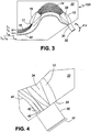
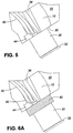
invention 103, shown in Fig. 3 reduces the range of X-Y displacement necessary to tune the AWG. In this embodiment, the input waveguide comprises one or moreintegrated waveguides 40 formed in the substrate with the AWG itself. In order to position the waveguide ends of theinput waveguides 40 close to the input point, theplanar waveguide 12 is reduced to its minimal dimensions to accommodate theinput waveguides 40. Thecone 34 of the propagating wavefront defines the minimal dimensions, andinput waveguides 40 can be positioned on one side or both of thecone 34 beside the modifiedplanar waveguide 12. In this arrangement X is fixed by the plane of the waveguide in the substrate and Y is fixed by the design of the photomask. It is preferred to launch an input signal from an integrated waveguide over fiber, because the mode field width of the integrated waveguide is well defined, providing more accurate control of the bandwidth of the device. Fiber has a mode field width accuracy of only ± 10 %. In the past it has been necessary to use fiber as an input waveguide to facilitate tuning. This invention facilitates a design which is more compact, and easier to assemble, as the polishing and pigtailing of fibers, all at one substrate edge, can be done at the same time. - As shown in Figs. 4 and 5, the invention, when implemented with integrated input waveguides permits the integration of many different inputs with varying parameters. It is then possible to select the best input waveguide by moving the lens assembly in the X direction. One of the parameters that can be varied is the width at the end of the waveguide inputs by tapering the waveguide ends 42, as shown in Fig. 4. The
taper 42 provides additional control or variation to the mode field width, and the resulting bandwidth of the device. By providing a plurality of input waveguides with different taper dimensions, a best input can be selected by positioning the lens assembly symmetrically between the selectedwaveguide 40 and the selected input point. - A further parameter to vary the input characteristics is shown in Fig. 5. The length of the slab or
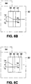
planar waveguide 12 can be adjusted by incorporating slab or planarwaveguide length increments 44 onto theinput waveguides 40.Different slab increments 44 are shown with stepped lengths from the substrate edgel9. Thewavefront cone 34 in theplanar waveguide 12 is no longer a point source at theinput plane 20, since the diverging wavefront begins at theslab increment 44. This provides selective adjustment in the Z axis. By increasing theslab increment 44, the pitch is increased. In this way it is possible to fix an exact channel pitch without introducing excess losses. The polishing tolerance is also reduced, since for the same polishing position, one can select many different slab lengths. - These parameters of waveguide position, taper dimension and slab increment can be combined and varied among a plurality of input waveguides to provide flexibility in tuning an AWG device.
- A reflective input assembly in accordance with the present invention is compatible with incorporating a
birefringence module 50 at theinput plane 20 as shown in Fig. 6a. Thebirefringence module 50 provides compensation for polarization effects within the AWG, including polarization dependent wavelength, polarization mode dispersion, and in the embodiment shown in Fig. 6c, polarization dependent loss. - More detailed discussion of the
birefringence module 50 can be found in the copending application 10-467, assigned to a common owner, herein incorporated by reference. - Fig. 6b shows a
birefringence module 50, including a first birefringent element 52 a half-wave plate 54 and a secondbirefringent element 56, in which the optical path lengths of the TE and TM polarization states are substantially equal. By changing the axes of thebirefringent elements crystal birefringence module 50 can provide compensation for polarization mode dispersion and polarization dependent wavelength. - Fig. 6c shows an alternative embodiment of the birefringence module 50' including a
polarizer 58 at the end face of the module 50' where the beams are combined. Thepolarizer 58 is selected to have an extinction ratio between the two polarization states to compensate for polarization dependent loss in the AWG. Thus, if the intensity of light of the two polarization states is not equal after passing through the AWG, apolarizer 58 can be selected to absorb a portion of the less attenuated polarization state at the output of the birefringence module 50'. - For some AWG designs, the distance between the
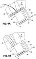
inputs 40 and the input point at the middle of theplanar waveguide 12 will be too large for a graded index lens. In order to increase the offset, the lens assembly is modified to include twolenses 30 and a corner mirror 32', as shown in Figs. 7 and 8c. Figs. 8a and 8b illustrate alternative lens assemblies. - Despite initial tuning, changes in temperature can cause the center wavelength of an AWG to shift because the refractive index of the phased array changes in response to temperature. This causes the position of the phase front leaving the device to shift. As a result, incomplete channel coupling occurs at the output waveguides. The reflective coupling in accordance with the present invention can incorporate additional thermal compensation.
- Fig. 9a and b illustrate an athermal
reflective coupling 60 comprising a thermally actuated pivot mechanism for supporting themirror 32. Theathermal coupling 60 includes afirst arm 62 of a material having a first coefficient of thermal expansion and asecond arm 64 of a different material having a second coefficient of thermal expansion. Eacharm substrate edge 19, or another common reference plane. Thefirst arm 62 supports amirror frame 66 which is coupled to thesecond arm 64 at one side, and which carries themirror 32 on another side of thefirst arm 62. A flex orpivot point 68 at thefirst arm 62 forms arotation center 68 about which themirror frame 66 pivots in response to differential expansion of the first andsecond arms mirror 32 as a collimated beam from thelens 30. The collimated beam is reflected back into thelens 30 at an angle determined by the pivot of theathermal coupling 60. The angle is translated by thelens 30 as an offset, thus shifting the input point at theinput plane 20. Of course, materials of different coefficients of expansion can be used to introduce a tilt to themirror 32 in many configurations that will be apparent to the person skilled in the art. The athermal input apparatus is discussed in greater detail in copending application No. 10-336, assigned to a common owner, herein incorporated by reference. - Numerous other embodiments can be envisaged without departing from the spirit and scope of the invention, which is defined in the claims.
Claims (10)
- An arrayed waveguide grating for spatially separating an optical signal including a plurality of wavelength channels comprising:a substrate for supporting an integrated arrayed waveguide grating formed therein including:an input planar waveguide, having an input plane at an edge of the substrate and an output plane, for propagating a wavefront from an input point on the input plane to an output plane;a grating comprising an array of waveguides optically coupled to the output plane of the input planar waveguide for receiving the wavefront, an optical length of the waveguides differing by a substantially equal amount from a first waveguide to an nth waveguide; and,an output planar waveguide for focusing separated wavelength signals on an output plane of the output planar waveguide for coupling to output waveguides;an input assembly for launching a signal into the integrated arrayed waveguide grating including:at least one input waveguide disposed on a plane substantially parallel to the input planar waveguide having a waveguide end for launching a signal into an input point on the input planar waveguide;a lens assembly including lens means symmetrically disposed between the coupled input point and the waveguide end of a selected one of the at least one waveguide, and a reflective element optically coupled to the lens means, the lens assembly for providing a lateral offset to a signal propagating from the input waveguide to the planar waveguide, and for focusing a reflected input signal at the input point of the input planar waveguide.
- An arrayed waveguide grating as defined in claim 1, wherein the at least one input waveguide comprises a plurality of integrated waveguides formed in the substrate with the integrated arrayed waveguide grating, each a selected different distance from the input planar waveguide to provide selective adjustment of a central wavelength response of the device.
- An arrayed waveguide grating as defined in claim 2, wherein the plurality of input waveguides each have an end portion having an increasing tapered width.
- An arrayed waveguide grating as defined in claim 3, wherein the at least one input waveguide includes a planar waveguide portion between the waveguide end and the lens.
- An arrayed waveguide grating as defined in claim 1, wherein the lens assembly comprises a pair of matched lenses symmetrically disposed between the coupled input point and the waveguide end of a selected one of the at least one waveguide, and a corner mirror for providing a larger lateral offset for a signal propagating between the input waveguide end and the input point.
- An arrayed waveguide grating as defined in claim 1, wherein the reflective element is supported by a thermally actuated tilt mechanism for coupling reflected light to the lens means at an angle to impart an offset to the focused light at the input point in response to temperature.
- An arrayed waveguide as defined in claim 1 for combining a plurality of wavelength channels, wherein a plurality of output waveguides are provided for launching the plurality of wavelength channels and wherein the at least one input waveguide is provided for outputting a combined optical signal.
- An arrayed waveguide grating as defined in claim 1, wherein the lens means comprises a lens having an optical axis symmetrically disposed between the coupled input point and the waveguide end of a selected one of the at least one waveguide.
- An arrayed waveguide grating as defined in claim 2, wherein the input planar waveguide is narrowed to accommodate the at least one input waveguide end face closely adjacent the input point without interfering with the diverging wavefront.
- An arrayed waveguide grating as defined in claim 2, wherein the plurality of input waveguides have among them at least one varying coupling parameter selected from the group consisting of: input position, waveguide taper and planar waveguide length increment.
Applications Claiming Priority (2)
| Application Number | Priority Date | Filing Date | Title |
|---|---|---|---|
| US19857300P | 2000-04-20 | 2000-04-20 | |
| US198573P | 2000-04-20 |
Publications (1)
| Publication Number | Publication Date |
|---|---|
| EP1148362A1 true EP1148362A1 (en) | 2001-10-24 |
Family
ID=22733943
Family Applications (1)
| Application Number | Title | Priority Date | Filing Date |
|---|---|---|---|
| EP01303543A Withdrawn EP1148362A1 (en) | 2000-04-20 | 2001-04-18 | Arrayed waveguide grating having a reflective input coupling |
Country Status (5)
| Country | Link |
|---|---|
| US (2) | US6701043B2 (en) |
| EP (1) | EP1148362A1 (en) |
| JP (1) | JP2002022982A (en) |
| CN (1) | CN1318764A (en) |
| CA (2) | CA2344609A1 (en) |
Families Citing this family (42)
| Publication number | Priority date | Publication date | Assignee | Title |
|---|---|---|---|---|
| EP1148362A1 (en) * | 2000-04-20 | 2001-10-24 | JDS Uniphase Inc. | Arrayed waveguide grating having a reflective input coupling |
| AU2002226873A1 (en) * | 2000-07-14 | 2002-04-08 | Applied Wdm, Inc. | Optical waveguide transmission devices |
| US6853769B2 (en) * | 2001-03-16 | 2005-02-08 | Lightwave Microsystems Corporation | Arrayed waveguide grating with waveguides of unequal widths |
| EP1384101B1 (en) * | 2001-04-30 | 2007-02-21 | Finisar Corporation | Arrangement for multiplexing and/or demultiplexing the signals of at least two optical wavelength channels |
| US20030039008A1 (en) * | 2001-08-27 | 2003-02-27 | Michael Davies | Optical grating for coarse wavelength division multiplexing (CWDM) applications |
| US6792182B1 (en) * | 2001-08-28 | 2004-09-14 | Metrophotonics, Inc. | Optical cross connect device with single grating |
| DE10146006A1 (en) * | 2001-09-19 | 2003-04-03 | Cube Optics Ag | Method for temperature compensation of an optical WDM component and optical WDM component with temperature compensation |
| US7444048B2 (en) * | 2001-10-09 | 2008-10-28 | Infinera Corporation | Tilted combiners/decombiners and photonic integrated circuit (PIC) employing the same |
| US6603892B1 (en) | 2001-10-24 | 2003-08-05 | Lightwave Microsystems Corporation | Mechanical beam steering for optical integrated circuits |
| US6853797B2 (en) * | 2001-11-05 | 2005-02-08 | Kotura, Inc. | Compact optical equalizer |
| EP1326107A3 (en) * | 2002-01-04 | 2004-03-10 | JDS Uniphase Corporation | Athermal optical coupler |
| US6738545B1 (en) * | 2002-03-18 | 2004-05-18 | Lightwave Microsystems Corporation | Athermal AWG and AWG with low power consumption using groove of changeable width |
| US6975793B2 (en) * | 2002-03-18 | 2005-12-13 | Lightwave Microsystems Corporation | Method and apparatus facilitating mechanical beam steering for optical integrated circuits |
| DE10222774C1 (en) * | 2002-05-16 | 2003-12-11 | Infineon Technologies Ag | Optical data channel multiplexing and/or demultiplexing device using arrayed waveguide grating and optical coupling device |
| US7305162B2 (en) * | 2002-05-30 | 2007-12-04 | Intel Corporation | Reducing the temperature sensitivity of optical waveguide interference filters |
| US7747114B2 (en) * | 2002-10-08 | 2010-06-29 | Infinera Corporation | Tilted combiners/decombiners and photonic integrated circuits (PICs) employing the same |
| US7412121B2 (en) * | 2002-10-24 | 2008-08-12 | Applied Research And Photonics, Inc. | Nanophotonic integrated circuit and fabrication thereof |
| US7110627B2 (en) * | 2002-10-24 | 2006-09-19 | Applied Research & Photonics, Inc. | Reflective arrayed waveguide grating |
| US7280722B2 (en) * | 2004-01-30 | 2007-10-09 | Texas Tech University | Temperature compensated optical multiplexer |
| EP1743201B1 (en) * | 2004-05-05 | 2020-10-14 | NeoPhotonics Corporation | Athermal awg and awg with low power consumption using groove of changeable width |
| US20070280605A1 (en) * | 2006-05-31 | 2007-12-06 | Mendoza Edgar A | Fiber bragg grating sensor interrogator and manufacture thereof |
| US8064744B2 (en) * | 2006-11-10 | 2011-11-22 | Rpo Pty Limited | Planar waveguide lens design |
| CN101419313B (en) * | 2008-10-31 | 2010-10-13 | 武汉光迅科技股份有限公司 | Method for manufacturing afebrile array wave-guide grating based on flat-plate wave-guide movement |
| JP2011034056A (en) * | 2009-07-08 | 2011-02-17 | Furukawa Electric Co Ltd:The | Arrayed waveguide diffraction grating type optical multiplexer/demultiplexer |
| US8611742B2 (en) | 2011-03-15 | 2013-12-17 | Capella Photonics, Inc. | Wavelength switch system using angle multiplexing optics |
| US9110232B2 (en) | 2011-06-03 | 2015-08-18 | Neophotonics Corporation | Thermally compensated arrayed waveguide grating assemblies |
| US8538212B2 (en) * | 2011-06-03 | 2013-09-17 | Neophotonics Corporation | Thermally compensated arrayed waveguide grating assemblies |
| CN102253448B (en) * | 2011-08-02 | 2012-10-17 | 浙江大学 | Method for realizing uniform polarization compensation of array waveguide grating |
| US9025912B2 (en) * | 2012-06-29 | 2015-05-05 | Infinera Corporation | Polarization material on an optical multiplexer or an optical demultiplexer |
| US9285538B2 (en) | 2012-10-23 | 2016-03-15 | Lumentum Operations Llc | Reducing temperature drift of an arrayed waveguide grating |
| CN103549941B (en) * | 2013-11-04 | 2015-05-20 | 天津工业大学 | AWG (arrayed waveguide grating) wavelength demodulation system with temperature compensation function, heartbeat detection device and application |
| CN103926654B (en) * | 2014-04-25 | 2017-06-06 | 珠海保税区光联通讯技术有限公司 | Afebrile array waveguide grating wavelength division multiplexer |
| KR102290188B1 (en) * | 2015-01-30 | 2021-08-20 | 한국전자통신연구원 | Wavelength combiner unit and arrayed waveguide grating having the same |
| US9927575B2 (en) * | 2015-06-25 | 2018-03-27 | Huawei Technologies Co., Ltd. | Optical coupling using polarization beam displacer |
| WO2017015578A1 (en) | 2015-07-22 | 2017-01-26 | Miroslaw Florjanczyk | Compound semiconductor photonic integrated circuit with dielectric waveguide |
| KR101885498B1 (en) * | 2018-01-24 | 2018-08-03 | 주식회사 폴스랩 | Athermal arrayed waveguide grating using precision parallel movement module and manufacturing method thereof |
| CN110658585B (en) | 2018-06-29 | 2022-01-11 | 华为技术有限公司 | Optical waveguide device |
| CN111988091B (en) | 2019-05-24 | 2022-04-05 | 华为技术有限公司 | Spatial light coupling device |
| US11726335B2 (en) | 2019-07-22 | 2023-08-15 | Apple Inc. | Head-mountable device with optical alignment |
| US11320598B2 (en) * | 2019-11-24 | 2022-05-03 | Applied Optoelectronics, Inc. | Optical demultiplexer with truncated profile and an optical transceiver module implementing same |
| CN115480347A (en) * | 2021-06-15 | 2022-12-16 | 中国科学院长春光学精密机械与物理研究所 | Method for improving verticality of array waveguide fiber and slab waveguide in wavelength division multiplexer |
| CN113448011B (en) * | 2021-06-29 | 2022-07-05 | 武汉光迅科技股份有限公司 | Design method and device of athermal AWG |
Citations (4)
| Publication number | Priority date | Publication date | Assignee | Title |
|---|---|---|---|---|
| US5732171A (en) * | 1994-06-28 | 1998-03-24 | Siemens Aktiengesellschaft | Device for spatially separating and/or joining optical wave channels |
| JPH11326975A (en) * | 1998-05-14 | 1999-11-26 | Nippon Telegr & Teleph Corp <Ntt> | Optical signal processing circuit and optical signal processing method |
| US6011885A (en) * | 1997-12-13 | 2000-01-04 | Lightchip, Inc. | Integrated bi-directional gradient refractive index wavelength division multiplexer |
| JP2000098148A (en) * | 1998-09-17 | 2000-04-07 | Nippon Telegr & Teleph Corp <Ntt> | Ultra-fast optical signal processing circuit |
Family Cites Families (7)
| Publication number | Priority date | Publication date | Assignee | Title |
|---|---|---|---|---|
| US5081615A (en) * | 1988-12-16 | 1992-01-14 | Fuji Photo Film Co., Ltd. | Method of coupling external light into an optical waveguide and a guided wave from an optical waveguide and optical pickup employing an optical waveguide |
| US6069990A (en) * | 1997-11-27 | 2000-05-30 | Hitachi Cable Ltd. | Optical wavelength multiplexer/demultiplexer |
| US5905824A (en) | 1997-12-09 | 1999-05-18 | Delisle; Vincent | Temperature compensated insensitive optical multiplexor/demultiplexor |
| US5920663A (en) | 1997-12-24 | 1999-07-06 | Lucent Technologies Inc. | Optical waveguide router with controlled transmission characteristics |
| GB2334343A (en) * | 1998-02-13 | 1999-08-18 | Northern Telecom Ltd | Optical waveguide multiplexer/demultiplexer with diffraction gratings embracing one another |
| US6253011B1 (en) * | 1998-12-30 | 2001-06-26 | Mcdonnell Douglas Corporation | Micro-aligner for precisely aligning an optical fiber and an associated fabrication method |
| EP1148362A1 (en) * | 2000-04-20 | 2001-10-24 | JDS Uniphase Inc. | Arrayed waveguide grating having a reflective input coupling |
-
2001
- 2001-04-18 EP EP01303543A patent/EP1148362A1/en not_active Withdrawn
- 2001-04-18 US US09/836,459 patent/US6701043B2/en not_active Expired - Lifetime
- 2001-04-19 CA CA002344609A patent/CA2344609A1/en not_active Abandoned
- 2001-04-19 CA CA002344582A patent/CA2344582A1/en not_active Abandoned
- 2001-04-20 JP JP2001122828A patent/JP2002022982A/en active Pending
- 2001-04-20 CN CN01116663.0A patent/CN1318764A/en active Pending
- 2001-04-20 US US09/838,137 patent/US6798948B2/en not_active Expired - Lifetime
Patent Citations (4)
| Publication number | Priority date | Publication date | Assignee | Title |
|---|---|---|---|---|
| US5732171A (en) * | 1994-06-28 | 1998-03-24 | Siemens Aktiengesellschaft | Device for spatially separating and/or joining optical wave channels |
| US6011885A (en) * | 1997-12-13 | 2000-01-04 | Lightchip, Inc. | Integrated bi-directional gradient refractive index wavelength division multiplexer |
| JPH11326975A (en) * | 1998-05-14 | 1999-11-26 | Nippon Telegr & Teleph Corp <Ntt> | Optical signal processing circuit and optical signal processing method |
| JP2000098148A (en) * | 1998-09-17 | 2000-04-07 | Nippon Telegr & Teleph Corp <Ntt> | Ultra-fast optical signal processing circuit |
Non-Patent Citations (2)
| Title |
|---|
| PATENT ABSTRACTS OF JAPAN vol. 2000, no. 02 29 February 2000 (2000-02-29) * |
| PATENT ABSTRACTS OF JAPAN vol. 2000, no. 07 29 September 2000 (2000-09-29) * |
Also Published As
| Publication number | Publication date |
|---|---|
| US6701043B2 (en) | 2004-03-02 |
| US6798948B2 (en) | 2004-09-28 |
| CA2344582A1 (en) | 2001-10-20 |
| CN1318764A (en) | 2001-10-24 |
| US20010033714A1 (en) | 2001-10-25 |
| JP2002022982A (en) | 2002-01-23 |
| US20010033715A1 (en) | 2001-10-25 |
| CA2344609A1 (en) | 2001-10-20 |
Similar Documents
| Publication | Publication Date | Title |
|---|---|---|
| US6701043B2 (en) | Arrayed waveguide grating having a reflective input coupling | |
| JP3434489B2 (en) | Array waveguide type diffraction grating | |
| CN1656721B (en) | Reconfigurable optical add-drop module device | |
| TWI416185B (en) | Wavelength division multiplexer architecture | |
| JP2000503140A (en) | Wavelength multiplexer / demultiplexer with various propagation constants | |
| US6934431B2 (en) | Variable optical delay lines and methods for making same | |
| US6134359A (en) | Optical multiplexing/demultiplexing device having a wavelength dispersive element | |
| JPH04212111A (en) | Multi-port optical device | |
| JP2000241656A (en) | Multiple wavelength multi-sepatation device | |
| US20060159395A1 (en) | Optical compensator array for dispersive element arrays | |
| EP1055946A2 (en) | Tapered multimode interference coupler | |
| JP3448551B2 (en) | Array waveguide type diffraction grating | |
| US6587615B1 (en) | Wavelength multiplexer-demultiplexer having a wide flat response within the spectral passband | |
| US6671428B1 (en) | Wavelength selective optical cross switch and optical add/drop multiplexer using volume phase grating and array of micro electro mechanical mirrors | |
| US6477293B1 (en) | Multiplexer/demultiplexer for WDM optical signals | |
| US6238102B1 (en) | Multiaxial optical coupler | |
| US20050174919A1 (en) | Optical polarization controller | |
| US8094982B2 (en) | Fiber lens assembly for optical device | |
| EP0463779A1 (en) | Fibre optic waveguide beam splitter | |
| US6925227B2 (en) | Optical device | |
| US6018603A (en) | Optical demultiplexing/multiplexing device having a wavelength dependent element | |
| US7013065B2 (en) | Planar optical apparatus for setting the chromatic dispersion in an optical system | |
| WO2003046629A1 (en) | System and method for multiplexing and demultiplexing optical signals using diffraction gratings | |
| JP2023006057A (en) | Wavelength multiplexer/demultiplexer | |
| JP4123519B2 (en) | Optical waveguide and optical multiplexer / demultiplexer |
Legal Events
| Date | Code | Title | Description |
|---|---|---|---|
| PUAI | Public reference made under article 153(3) epc to a published international application that has entered the european phase |
Free format text: ORIGINAL CODE: 0009012 |
|
| AK | Designated contracting states |
Kind code of ref document: A1 Designated state(s): DE FR GB Kind code of ref document: A1 Designated state(s): AT BE CH CY DE DK ES FI FR GB GR IE IT LI LU MC NL PT SE TR |
|
| AX | Request for extension of the european patent |
Free format text: AL;LT;LV;MK;RO;SI |
|
| 17P | Request for examination filed |
Effective date: 20020424 |
|
| AKX | Designation fees paid |
Free format text: DE FR GB |
|
| GRAH | Despatch of communication of intention to grant a patent |
Free format text: ORIGINAL CODE: EPIDOS IGRA |
|
| GRAH | Despatch of communication of intention to grant a patent |
Free format text: ORIGINAL CODE: EPIDOS IGRA |
|
| STAA | Information on the status of an ep patent application or granted ep patent |
Free format text: STATUS: THE APPLICATION IS DEEMED TO BE WITHDRAWN |
|
| 18D | Application deemed to be withdrawn |
Effective date: 20031031 |