EP1150331A2 - Gas distribution plate assembly for providing laminar gas flow across the surface of a substrate - Google Patents
Gas distribution plate assembly for providing laminar gas flow across the surface of a substrate Download PDFInfo
- Publication number
- EP1150331A2 EP1150331A2 EP01303758A EP01303758A EP1150331A2 EP 1150331 A2 EP1150331 A2 EP 1150331A2 EP 01303758 A EP01303758 A EP 01303758A EP 01303758 A EP01303758 A EP 01303758A EP 1150331 A2 EP1150331 A2 EP 1150331A2
- Authority
- EP
- European Patent Office
- Prior art keywords
- baffle plate
- apertures
- lower baffle
- wafer
- plate assembly
- Prior art date
- Legal status (The legal status is an assumption and is not a legal conclusion. Google has not performed a legal analysis and makes no representation as to the accuracy of the status listed.)
- Withdrawn
Links
Images


Classifications
-
- H—ELECTRICITY
- H01—ELECTRIC ELEMENTS
- H01L—SEMICONDUCTOR DEVICES NOT COVERED BY CLASS H10
- H01L21/00—Processes or apparatus adapted for the manufacture or treatment of semiconductor or solid state devices or of parts thereof
-
- C—CHEMISTRY; METALLURGY
- C23—COATING METALLIC MATERIAL; COATING MATERIAL WITH METALLIC MATERIAL; CHEMICAL SURFACE TREATMENT; DIFFUSION TREATMENT OF METALLIC MATERIAL; COATING BY VACUUM EVAPORATION, BY SPUTTERING, BY ION IMPLANTATION OR BY CHEMICAL VAPOUR DEPOSITION, IN GENERAL; INHIBITING CORROSION OF METALLIC MATERIAL OR INCRUSTATION IN GENERAL
- C23C—COATING METALLIC MATERIAL; COATING MATERIAL WITH METALLIC MATERIAL; SURFACE TREATMENT OF METALLIC MATERIAL BY DIFFUSION INTO THE SURFACE, BY CHEMICAL CONVERSION OR SUBSTITUTION; COATING BY VACUUM EVAPORATION, BY SPUTTERING, BY ION IMPLANTATION OR BY CHEMICAL VAPOUR DEPOSITION, IN GENERAL
- C23C16/00—Chemical coating by decomposition of gaseous compounds, without leaving reaction products of surface material in the coating, i.e. chemical vapour deposition [CVD] processes
- C23C16/44—Chemical coating by decomposition of gaseous compounds, without leaving reaction products of surface material in the coating, i.e. chemical vapour deposition [CVD] processes characterised by the method of coating
- C23C16/455—Chemical coating by decomposition of gaseous compounds, without leaving reaction products of surface material in the coating, i.e. chemical vapour deposition [CVD] processes characterised by the method of coating characterised by the method used for introducing gases into reaction chamber or for modifying gas flows in reaction chamber
- C23C16/45563—Gas nozzles
- C23C16/45565—Shower nozzles
-
- H—ELECTRICITY
- H01—ELECTRIC ELEMENTS
- H01J—ELECTRIC DISCHARGE TUBES OR DISCHARGE LAMPS
- H01J37/00—Discharge tubes with provision for introducing objects or material to be exposed to the discharge, e.g. for the purpose of examination or processing thereof
- H01J37/32—Gas-filled discharge tubes
- H01J37/32431—Constructional details of the reactor
- H01J37/3244—Gas supply means
Definitions
- the present invention relates generally to the field of semiconductor plasma processing systems such as photoresist ashers, and more specifically to a gas distribution plate assembly for providing laminar gas flow across the surface of a substrate.
- photolithography techniques are used to form integrated circuit patterns on a substrate, such a silicon wafer.
- the substrate is coated with a photoresist, portions of which are exposed to ultraviolet (UV) radiation through a mask to image a desired circuit pattern on the photoresist.
- UV radiation ultraviolet
- the portions of the photoresist left unexposed to the UV radiation are removed by a processing solution, leaving only the exposed portions on the substrate. These remaining exposed portions are baked during a photostabilization process to enable the photoresist to withstand subsequent processing.
- the photoresist is “ashed” or “burned” and the ashed or burned photoresist, along with the residue, is “stripped” or “cleaned” from the surface of the substrate.
- One manner of removing photoresist and residues is by rapidly heating the photoresist-covered substrate in a vacuum chamber to a preset temperature by infrared radiation, and directing microwave-energized reactive gases (i . e ., a plasma) toward the heated substrate surface.
- the reactive plasma reacts with the photoresist to ash it for subsequent removal from the wafer.
- Process conditions that must be so controlled include the temperature of the process chamber and the temperature of the wafer.
- Known gas distribution or baffle plates for directing energized plasma toward a wafer are typically made of quartz, due to their ability to withstand high process temperatures.
- quartz makes acceptable wafer and process temperature uniformity difficult to obtain.
- the temperature non-uniformities are caused by the large temperature gradients that can develop across the surface of a quartz plate due to its poor thermal conductivity characteristics.
- undesirable infrared (IR) wavelength absorption characteristics of quartz add to the thermal energy absorbed by the baffle plate. As a result, process uniformity and system throughput are adversely affected.
- baffle plates such as that shown U.S. Patent No. 5,449,410 to Chang et al. distribute energized gases into the process chamber by means of a configuration that includes perimetric apertures but no apertures near the center (see Figure 2 of Chang).
- known baffle plates such as that shown suffer from an inability to evenly distribute gas across the surface of the wafer in a laminar flow-like manner, especially when high gas flow rates are provided to achieve corresponding high process rates.
- the flow of gas is such that reactive species are supplied to the surface of the wafer in a manner that provides a uniform reaction rate even at high gas flow rates. This is achieved by providing a ratio of laminar jet center velocity to jet expansion such that a uniform mass flow rate per unit area is provided to the surface of the wafer.
- the supply of reactive species to the surface of the wafer allows for the generation of reaction effluent emanating from the surface of the wafer as the reaction occurs.
- a baffle plate assembly is provided for distributing gas flow into an adjacent process chamber containing a semiconductor wafer to be processed.
- the baffle plate assembly comprises a generally planar upper baffle plate fixedly positioned above a generally planar lower baffle plate.
- a plenum is formed between the lower baffle plate and the process chamber lid or top wall.
- the lower baffle plate is sealed to the process chamber, and the process chamber top wall is attached to the lower baffle plate, creating a region of higher pressure in this plenum (as compared to the process chamber pressure).
- At least the lower baffle plate has a pattern of apertures formed therein for permitting gas to pass therethrough and into the wafer process chamber.
- the upper baffle plate and the lower baffle plate are positioned generally parallel to each other, and the upper baffle plate is smaller than the lower baffle plate.
- the lower baffle plate is comprised of low-alloy anodized aluminum
- the upper baffle plate is comprised of sapphire-coated quartz.
- the apertures in the lower baffle plate are arranged in a pattern such that each aperture is equidistant from any adjacent aperture.
- the upper baffle plate is provided with slightly larger apertures formed therein in a concentric multiply circular (radial) pattern.
- the upper baffle plate is also provided with a centrally located impingement plate.
- the apertures in the lower baffle plate are arranged in a concentric multiply circular (radial) pattem, and the upper baffle plate is apertureless.
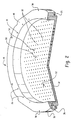
- Figure 1 shows an asher process chamber 10 into which is incorporated a first embodiment of a gas distribution or baffle plate assembly 12.
- the asher process chamber 10 having the baffle plate assembly 12 installed therein is suitable for use in a 300 millimeter (mm) wafer processing system.
- mm millimeter
- the present invention is shown as being implemented within a photoresist asher, it may also be used in other semiconductor manufacturing equipment, such as residue removal, stripping, and isotropic etching equipment.
- the baffle plate assembly 12 comprises an upper apertured baffle plate 14 and a relatively larger lower apertured baffle plate 16 positioned generally parallel to each other and separated from one another.
- the baffle plate assembly is attached to a lower portion 18 of the process chamber that includes a cavity 20 in which a wafer 22 to be processed is placed.
- the baffle plates 14 and 16, in addition to being oriented parallel to each other, are also oriented parallel to the wafer being processed.
- a seal 23 is provided at the interface between the baffle plate assembly 12 and the lower portion 18 of the process chamber, and resides within groove 25 in the lower baffle plate 16 (see Figure 2). Wafers are introduced into and removed from the process chamber via a load lock mechanism (not shown) via entry/exit passageway 24.
- a heater mechanism located under the lower portion 18 of the process chamber, heats the underside of the wafer to a desired temperature during processing.
- the asher process chamber 10 of Figure 1 is typically installed within an asher intermediate the heater assembly (below) and a plasma tube assembly (above, not shown) at the locations of holes 26.
- the plasma tube is typically made of alumina (Al 2 O 3 ) or sapphire to accommodate fluorine chemistries without etching or other degradation.
- a desired mixture of gases is introduced into the plasma tube from a gas box.
- a desired gas mixture is forming gas (primarily nitrogen with a small percentage of hydrogen), and oxygen.
- a fluorine-containing gas such as carbon tetrafluoride (CF 4 ) may be added to the gas mixture to increase ashing rates for certain processes.
- the desired gas mixture is energized in the plasma tube by a microwave power generator assembly to form a reactive plasma that will ash photoresist on a wafer residing in the process chamber cavity 20.
- Energized plasma typically leaves the plasma tube and is directed into the process chamber 10 at approximately an atmospheric pressure of 1.6 torr and a temperature of about 150° C.
- there is a drop in pressure along the length of the plasma tube which directs the plasma downward through the tube and toward the process chamber 10.
- the energized plasma (gas) leaving the plasma tube encounters the baffle plate assembly 12.
- the plasma is distributed into the process chamber cavity 20 via apertures 28 in the upper baffle plate 14 and apertures 30 in the lower baffle plate 16.
- the lower baffle plate 16 may be actively cooled with a cooling medium flowing through internal cooling passages 32 via inlets 34 and outlets 36 (see also Figure 2).
- the walls 38 of the lower portion 18 of the process chamber may also be actively cooled with a cooling medium flowing through internal cooling passages 40 via inlet 42 and outlet 44.
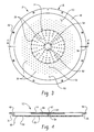
- the lower baffle plate 16 as shown in the partial cutaway, perspective view of Figure 2, comprises an outer flange 48 and a generally planar portion 50 which contains the apertures 30.
- Mounting holes 52 are provided in the lower baffle plate 16 for mounting the upper baffle plate 14 thereto by means of standoffs 54 (shown in Figures 4 and 6). The distance between the upper and lower baffle plates in part determines the pattern of gas flow through the baffle plate assembly 12.
- FIG 3 is a plan view of the 300 mm baffle plate assembly shown in Figure 1
- Figure 4 is a sectional view of this embodiment of the baffle plate assembly.
- the baffle plate assembly is mounted to the lower portion 18 of the process chamber via mounting holes 56 in the lower baffle plate flange 48.
- the generally planar portion 50 of the lower baffle plate 16 includes a radially inner portion 58 and a radially external portion 60.
- Apertures 30 are provided in the radially inner portion 58 of the lower baffle plate but not in the radially external portion 60.
- the surface area of the radially inner portion 58 is sufficient to cover the wafer 22 residing therebelow (see Figure 1).
- the apertures are positioned equidistant from each other in all directions. That is, any three apertures which are mutually immediately adjacent to each other form an equilateral triangle.
- the apertures 28 in the upper baffle plate 14 are arranged in a radial (or concentric multiply circular) pattern.
- the upper baffle plate is comprised of sapphire-coated fused silica or quartz (SiO 2 ).
- the apertures 28 in the upper baffle plate 14 are slightly larger than the apertures 30 in the lower baffle plate 16.
- Located at the center of the upper baffle plate is a sapphire impingement plate 62, which is attached to the upper baffle plate using screws 64.
- the sapphire impingement plate 62 diverts energized gases emanating from the plasma tube radially outward to the remaining apertured area of the upper baffle plate 14, so as to prevent the radially inward potion of the wafer 22 being processed from overheating.
- FIGS 5 and 6 show a second embodiment of the baffle plate assembly 12, which is installable into the photoresist asher process chamber of Figure 1 for 200 mm wafer process applications.
- the lower baffle plate 16 has apertures 30 formed in the radially inner portion 58 in a radial (or concentric multiply circular) pattern. The surface area of the radially inner portion 58 is sufficient to cover the wafer 22 residing in the process chamber therebelow.
- the upper baffle plate 14 is apertureless.
- the centrally located sapphire impingement plate 62 remains in this embodiment.
- the upper baffle plate in this embodiment like the 300 mm embodiment, is comprised of a sapphire-coated fused silica (quartz).
- the lower baffle plate 16 in either the 200 mm or 300 mm embodiments, is preferably formed from a single piece of low-alloy anodized aluminum (e.g. , Alcoa type C-276), which significantly improves the heat transfer characteristics and corrosion resistance of the baffle plate over known quartz baffle plates.
- the use of aluminum also permits the cooling passages to be drilled or machined directly therein, thereby making the baffle plate less sensitive to inconsistencies in the heating system, and allows the process occurring on the surface of the wafer to take place at a substantially uniform temperature.
- the use of aluminum also blocks a large percentage of ultraviolet (UV) energy emanating from the heating system that would otherwise make temperature control more difficult and possibly cause wafer device damage.
- UV ultraviolet
- the baffle plate assembly 12 of the present invention evenly distributes the reactive plasma received from the plasma tube across the surface of the wafer 22 being processed to achieve desired process results.
- the inventive baffle plate assembly enhances the uniformity of plasma ions and radical densities that pass across the wafer surface during processing, providing for improved process uniformity while maintaining high wafer throughput rates.
- the design of the individual baffle plates and of the baffle plate assembly is determined by applied gas dynamics, materials engineering, and process data to insure correct pressure, gas flows and temperature gradients within the process chamber.
- the baffle plate assembly is compact, requiring less than one inch vertical space within the process chamber 10.
- the baffle plate assembly construction together with an incremental pressure drop from just above the upper baffle plate 14 to just below the lower baffle plate 16, helps create a laminar flow of gas which is distributed across the upper surface of the wafer 22 being processed.
- the baffle plate assembly 12 minimizes the mass flow rate gradient per unit area across the surface of the lower baffle plate in a direction normal to the surface of the plate. This is accomplished by combining the effects of radial pressure drop between the upper plate and the process chamber top wall 17 (see Figure 1), between the upper and lower plates, and the effect of the pressure drop across the plane defined by the lower baffle plate.
- the effect is to provide a uniform distribution of reactive species to the surface of the wafer and to allow for the generation of reaction effluent emanating from the surface of the wafer as the reaction takes place.
- the combination of the sapphire-coated quartz upper plate 14 and the aluminum lower plate 16 in the baffle plate assembly 12 has been found to be suitable for use in the harsh conditions found in a process chamber used for photoresist removal, even when corrosive gases such as CF 4 are utilized.
- the baffle plate assembly functions in operation as follows. Energized gas output from the end of the plasma tube (at approximately 1.6 torr) flows at a rate of about 5-7 litres per minute (Ipm).
- the sapphire impingement plate 62 on the upper baffle plate 14 first functions to distribute reactive gases radially outward, causing a radial pressure drop. Radial pressure drop is a function of the spacing between the upper and lower baffle plates, the size and pattem of apertures in these plates, and the size and shape of these plates.
- the upper baffle plate 14 also protects the lower baffle plate 16 from damage by the plasma.
- the pressure at the surface of the impingement plate 62 and the upper baffle plate 14 is approximately 1.5 torr.
- the pressure of the area 66 between the upper and lower baffle plates is approximately 1.2 - 1.3 torr.
- the pressure below the lower baffle plate 16, within the process chamber cavity 20, is on the order of 1.0 torr. This incremental pressure drop from the plasma tube exit to the process chamber cavity 20 insures a downward flow of gas, and the baffle plate assembly construction imparts a laminar flow characteristic to this downwardly flowing gas.
- the incremental vertical pressure drop is a function of the number and size of the apertures in the upper and lower baffle plates, the aperture location, and the assembly geometry. Because the pressure drop across the lower baffle plate is known a maximum 5% ashing rate non-uniformity has been achieved across the surface of an ashed wafer processed by the inventive baffle plate assembly.
Abstract
Description
- The following U.S. patent application is incorporated by reference herein as if it had been fully set forth: Application Serial Number: 560,538, filed on 26 April 2000, entitled Actively-Cooled Distribution Plate for Reducing Reactive Gas Temperature in a Plasma Processing System (corresponding to a European patent application filed simultaneously herewith, agents reference J42380EP).
- The present invention relates generally to the field of semiconductor plasma processing systems such as photoresist ashers, and more specifically to a gas distribution plate assembly for providing laminar gas flow across the surface of a substrate.
- In the manufacture of integrated circuits, photolithography techniques are used to form integrated circuit patterns on a substrate, such a silicon wafer. Typically, the substrate is coated with a photoresist, portions of which are exposed to ultraviolet (UV) radiation through a mask to image a desired circuit pattern on the photoresist. The portions of the photoresist left unexposed to the UV radiation are removed by a processing solution, leaving only the exposed portions on the substrate. These remaining exposed portions are baked during a photostabilization process to enable the photoresist to withstand subsequent processing.
- After such processing, in which the integrated circuit components are formed, it is generally necessary to remove the baked photoresist from the wafer. In addition, residue that has been introduced on the substrate surface through processes such as etching must be removed. Typically, the photoresist is "ashed" or "burned" and the ashed or burned photoresist, along with the residue, is "stripped" or "cleaned" from the surface of the substrate.
- One manner of removing photoresist and residues is by rapidly heating the photoresist-covered substrate in a vacuum chamber to a preset temperature by infrared radiation, and directing microwave-energized reactive gases (i.e., a plasma) toward the heated substrate surface. In the resulting process, the reactive plasma reacts with the photoresist to ash it for subsequent removal from the wafer.
- It is important that the ashing process occur at substantially the same rate across the surface of the wafer. To insure such uniform ashing of the photoresist, the process conditions must be precisely controlled. Process conditions that must be so controlled include the temperature of the process chamber and the temperature of the wafer.
- Known gas distribution or baffle plates for directing energized plasma toward a wafer are typically made of quartz, due to their ability to withstand high process temperatures. However, the use of quartz makes acceptable wafer and process temperature uniformity difficult to obtain. The temperature non-uniformities are caused by the large temperature gradients that can develop across the surface of a quartz plate due to its poor thermal conductivity characteristics. In addition, undesirable infrared (IR) wavelength absorption characteristics of quartz add to the thermal energy absorbed by the baffle plate. As a result, process uniformity and system throughput are adversely affected.
- In addition to precise temperature control, the energized plasma that reacts with the photoresist must be evenly distributed across the wafer while a constant gas flow rate is maintained. Known baffle plates such as that shown U.S. Patent No. 5,449,410 to Chang et al. distribute energized gases into the process chamber by means of a configuration that includes perimetric apertures but no apertures near the center (see Figure 2 of Chang). However, known baffle plates such as that shown suffer from an inability to evenly distribute gas across the surface of the wafer in a laminar flow-like manner, especially when high gas flow rates are provided to achieve corresponding high process rates.
- Thus, it is an object of the present invention to provide a mechanism for enabling a laminar flow of energized gas across the surface of a substrate being processed in a plasma processing system. The flow of gas is such that reactive species are supplied to the surface of the wafer in a manner that provides a uniform reaction rate even at high gas flow rates. This is achieved by providing a ratio of laminar jet center velocity to jet expansion such that a uniform mass flow rate per unit area is provided to the surface of the wafer. In addition, the supply of reactive species to the surface of the wafer allows for the generation of reaction effluent emanating from the surface of the wafer as the reaction occurs. It is a further object of the invention to improve wafer-to-wafer process uniformity in such a system. It is still a further object of the invention to provide a mechanism for minimizing temperature gradients across the wafer by providing a relatively flat temperature profile, across the surface of a gas distribution or baffle plate in such a system.
- A baffle plate assembly is provided for distributing gas flow into an adjacent process chamber containing a semiconductor wafer to be processed. The baffle plate assembly comprises a generally planar upper baffle plate fixedly positioned above a generally planar lower baffle plate. A plenum is formed between the lower baffle plate and the process chamber lid or top wall. The lower baffle plate is sealed to the process chamber, and the process chamber top wall is attached to the lower baffle plate, creating a region of higher pressure in this plenum (as compared to the process chamber pressure). At least the lower baffle plate has a pattern of apertures formed therein for permitting gas to pass therethrough and into the wafer process chamber. The upper baffle plate and the lower baffle plate are positioned generally parallel to each other, and the upper baffle plate is smaller than the lower baffle plate. Preferably, the lower baffle plate is comprised of low-alloy anodized aluminum, and the upper baffle plate is comprised of sapphire-coated quartz.
- In a 300 millimeter (mm) embodiment, the apertures in the lower baffle plate are arranged in a pattern such that each aperture is equidistant from any adjacent aperture. The upper baffle plate is provided with slightly larger apertures formed therein in a concentric multiply circular (radial) pattern. The upper baffle plate is also provided with a centrally located impingement plate. In a 200 mm embodiment, the apertures in the lower baffle plate are arranged in a concentric multiply circular (radial) pattem, and the upper baffle plate is apertureless.
-
- Figure 1 is a partial cutaway, perspective view of a photoresist asher process chamber into which is installed a first embodiment of a baffle plate assembly constructed according to the present invention;
- Figure 2 is a partial cutaway, perspective view of the lower baffle plate portion of the baffle plate assembly of Figure 1, shown in its water-cooled embodiment;
- Figure 3 is a plan view of the baffle plate assembly shown in Figure 1, shown in its water-cooled embodiment;
- Figure 4 is a sectional view of the baffle plate assembly of Figure 3, taken along the lines 4-4;
- Figure 5 is a plan view of a second embodiment of a baffle plate assembly constructed according to the present invention, which is installable into the photoresist asher process chamber of Figure 1; and
- Figure 6 is a sectional view of the baffle plate assembly of Figure 5, taken along the lines 6-6.
-
- Referring now to the drawings, Figure 1 shows an
asher process chamber 10 into which is incorporated a first embodiment of a gas distribution orbaffle plate assembly 12. Theasher process chamber 10 having thebaffle plate assembly 12 installed therein is suitable for use in a 300 millimeter (mm) wafer processing system. Although the present invention is shown as being implemented within a photoresist asher, it may also be used in other semiconductor manufacturing equipment, such as residue removal, stripping, and isotropic etching equipment. - The
baffle plate assembly 12 comprises an upper aperturedbaffle plate 14 and a relatively larger lowerapertured baffle plate 16 positioned generally parallel to each other and separated from one another. The baffle plate assembly is attached to alower portion 18 of the process chamber that includes acavity 20 in which awafer 22 to be processed is placed. Thebaffle plates - A
seal 23 is provided at the interface between thebaffle plate assembly 12 and thelower portion 18 of the process chamber, and resides withingroove 25 in the lower baffle plate 16 (see Figure 2). Wafers are introduced into and removed from the process chamber via a load lock mechanism (not shown) via entry/exit passageway 24. A heater mechanism (not shown), located under thelower portion 18 of the process chamber, heats the underside of the wafer to a desired temperature during processing. - The
asher process chamber 10 of Figure 1 is typically installed within an asher intermediate the heater assembly (below) and a plasma tube assembly (above, not shown) at the locations ofholes 26. The plasma tube is typically made of alumina (Al2O3) or sapphire to accommodate fluorine chemistries without etching or other degradation. In operation, a desired mixture of gases is introduced into the plasma tube from a gas box. - One example of a desired gas mixture is forming gas (primarily nitrogen with a small percentage of hydrogen), and oxygen. A fluorine-containing gas such as carbon tetrafluoride (CF4) may be added to the gas mixture to increase ashing rates for certain processes. The desired gas mixture is energized in the plasma tube by a microwave power generator assembly to form a reactive plasma that will ash photoresist on a wafer residing in the
process chamber cavity 20. Energized plasma typically leaves the plasma tube and is directed into theprocess chamber 10 at approximately an atmospheric pressure of 1.6 torr and a temperature of about 150° C. Typically there is a drop in pressure along the length of the plasma tube which directs the plasma downward through the tube and toward theprocess chamber 10. - The energized plasma (gas) leaving the plasma tube encounters the
baffle plate assembly 12. The plasma is distributed into theprocess chamber cavity 20 viaapertures 28 in theupper baffle plate 14 andapertures 30 in thelower baffle plate 16. Thelower baffle plate 16 may be actively cooled with a cooling medium flowing throughinternal cooling passages 32 viainlets 34 and outlets 36 (see also Figure 2). Thewalls 38 of thelower portion 18 of the process chamber may also be actively cooled with a cooling medium flowing throughinternal cooling passages 40 via inlet 42 and outlet 44. - The
lower baffle plate 16, as shown in the partial cutaway, perspective view of Figure 2, comprises anouter flange 48 and a generallyplanar portion 50 which contains theapertures 30. Mountingholes 52 are provided in thelower baffle plate 16 for mounting theupper baffle plate 14 thereto by means of standoffs 54 (shown in Figures 4 and 6). The distance between the upper and lower baffle plates in part determines the pattern of gas flow through thebaffle plate assembly 12. - Figure 3 is a plan view of the 300 mm baffle plate assembly shown in Figure 1, and Figure 4 is a sectional view of this embodiment of the baffle plate assembly. As shown in these Figures, the baffle plate assembly is mounted to the
lower portion 18 of the process chamber via mountingholes 56 in the lowerbaffle plate flange 48. The generallyplanar portion 50 of thelower baffle plate 16 includes a radiallyinner portion 58 and a radiallyexternal portion 60. -
Apertures 30 are provided in the radiallyinner portion 58 of the lower baffle plate but not in the radiallyexternal portion 60. Theapertures 30, although shown only partially covering the radiallyinternal portion 58, actually cover the entirety of this inner portion (see Figure 2). The surface area of the radiallyinner portion 58 is sufficient to cover thewafer 22 residing therebelow (see Figure 1). The apertures are positioned equidistant from each other in all directions. That is, any three apertures which are mutually immediately adjacent to each other form an equilateral triangle. - The
apertures 28 in theupper baffle plate 14 are arranged in a radial (or concentric multiply circular) pattern. The upper baffle plate is comprised of sapphire-coated fused silica or quartz (SiO2). Theapertures 28 in theupper baffle plate 14 are slightly larger than theapertures 30 in thelower baffle plate 16. Located at the center of the upper baffle plate is asapphire impingement plate 62, which is attached to the upper baffle plate using screws 64. Thesapphire impingement plate 62 diverts energized gases emanating from the plasma tube radially outward to the remaining apertured area of theupper baffle plate 14, so as to prevent the radially inward potion of thewafer 22 being processed from overheating. - Figures 5 and 6 show a second embodiment of the
baffle plate assembly 12, which is installable into the photoresist asher process chamber of Figure 1 for 200 mm wafer process applications. In this second embodiment, thelower baffle plate 16 hasapertures 30 formed in the radiallyinner portion 58 in a radial (or concentric multiply circular) pattern. The surface area of the radiallyinner portion 58 is sufficient to cover thewafer 22 residing in the process chamber therebelow. - In the 200 mm embodiment of the present invention of Figures 5 and 6, the
upper baffle plate 14 is apertureless. The centrally locatedsapphire impingement plate 62 remains in this embodiment. The upper baffle plate in this embodiment, like the 300 mm embodiment, is comprised of a sapphire-coated fused silica (quartz). - The
lower baffle plate 16, in either the 200 mm or 300 mm embodiments, is preferably formed from a single piece of low-alloy anodized aluminum (e.g., Alcoa type C-276), which significantly improves the heat transfer characteristics and corrosion resistance of the baffle plate over known quartz baffle plates. The use of aluminum also permits the cooling passages to be drilled or machined directly therein, thereby making the baffle plate less sensitive to inconsistencies in the heating system, and allows the process occurring on the surface of the wafer to take place at a substantially uniform temperature. The use of aluminum also blocks a large percentage of ultraviolet (UV) energy emanating from the heating system that would otherwise make temperature control more difficult and possibly cause wafer device damage. - In either of its 200 mm or 300 mm embodiments, the
baffle plate assembly 12 of the present invention evenly distributes the reactive plasma received from the plasma tube across the surface of thewafer 22 being processed to achieve desired process results. The inventive baffle plate assembly enhances the uniformity of plasma ions and radical densities that pass across the wafer surface during processing, providing for improved process uniformity while maintaining high wafer throughput rates. The design of the individual baffle plates and of the baffle plate assembly is determined by applied gas dynamics, materials engineering, and process data to insure correct pressure, gas flows and temperature gradients within the process chamber. The baffle plate assembly is compact, requiring less than one inch vertical space within theprocess chamber 10. - The baffle plate assembly construction, together with an incremental pressure drop from just above the
upper baffle plate 14 to just below thelower baffle plate 16, helps create a laminar flow of gas which is distributed across the upper surface of thewafer 22 being processed. Thebaffle plate assembly 12 minimizes the mass flow rate gradient per unit area across the surface of the lower baffle plate in a direction normal to the surface of the plate. This is accomplished by combining the effects of radial pressure drop between the upper plate and the process chamber top wall 17 (see Figure 1), between the upper and lower plates, and the effect of the pressure drop across the plane defined by the lower baffle plate. The effect is to provide a uniform distribution of reactive species to the surface of the wafer and to allow for the generation of reaction effluent emanating from the surface of the wafer as the reaction takes place. The combination of the sapphire-coated quartzupper plate 14 and the aluminumlower plate 16 in thebaffle plate assembly 12 has been found to be suitable for use in the harsh conditions found in a process chamber used for photoresist removal, even when corrosive gases such as CF4 are utilized. - The baffle plate assembly functions in operation as follows. Energized gas output from the end of the plasma tube (at approximately 1.6 torr) flows at a rate of about 5-7 litres per minute (Ipm). The
sapphire impingement plate 62 on theupper baffle plate 14 first functions to distribute reactive gases radially outward, causing a radial pressure drop. Radial pressure drop is a function of the spacing between the upper and lower baffle plates, the size and pattem of apertures in these plates, and the size and shape of these plates. Theupper baffle plate 14 also protects thelower baffle plate 16 from damage by the plasma. - The pressure at the surface of the
impingement plate 62 and theupper baffle plate 14 is approximately 1.5 torr. The pressure of thearea 66 between the upper and lower baffle plates is approximately 1.2 - 1.3 torr. The pressure below thelower baffle plate 16, within theprocess chamber cavity 20, is on the order of 1.0 torr. This incremental pressure drop from the plasma tube exit to theprocess chamber cavity 20 insures a downward flow of gas, and the baffle plate assembly construction imparts a laminar flow characteristic to this downwardly flowing gas. - The incremental vertical pressure drop is a function of the number and size of the apertures in the upper and lower baffle plates, the aperture location, and the assembly geometry. Because the pressure drop across the lower baffle plate is known a maximum 5% ashing rate non-uniformity has been achieved across the surface of an ashed wafer processed by the inventive baffle plate assembly.
- Accordingly, a preferred embodiment of a gas distribution plate assembly for providing a laminar gas flow across the surface of a substrate in a plasma processing system has been described. With the foregoing description in mind, however, it is understood that this description is made only by way of example, that the invention is not limited to the particular embodiments described herein, and that various rearrangements, modifications, and substitutions may be implemented with respect to the foregoing description without departing from the scope of the invention as defined by the following claims and their equivalents.
Claims (24)
- A plasma processing chamber (10) for processing a semiconductor wafer contained therein, comprising:(i) a wafer processing cavity (20) into which a wafer may be inserted for processing, the wafer processing cavity defined in part by walls (38) including a top wall (17); and(ii) a baffle plate assembly (12) located adjacent said wafer processing cavity for distributing energized gas thereinto, said baffle plate assembly comprising a generally planar upper baffle plate (14) fixedly positioned above a generally planar lower baffle plate (16), said top wall (17) and said lower baffle plate (16) forming a plenum therebetween; said plenum operating at a higher pressure than said processing cavity (20) during operation of the chamber (10); at least said lower baffle plate (16) having a pattern of apertures (30) formed therein for permitting gas to pass therethrough from said plenum and into said wafer processing cavity.
- The plasma processing chamber (10) of claim 1, wherein said upper baffle plate (14) and said lower baffle plate (16) are positioned generally parallel to each other and to the wafer being processed in cavity (20).
- The plasma processing chamber (10) of claim 2, wherein said lower baffle plate (16) is comprised of low-alloy anodized aluminum.
- The plasma processing chamber (10) of claim 3, wherein said upper baffle plate (14) is comprised of quartz.
- The plasma processing chamber (10) of claim 4, wherein said upper quartz baffle plate (14) is coated with sapphire.
- The plasma processing chamber (10) of claim 2, wherein the chamber (10) is adapted to receive a wafer having a diameter of approximately 300 millimeters (mm).
- The plasma processing chamber (10) of claim 6, wherein said apertures (30) in said lower baffle plate (16) are arranged in a pattern such that each aperture (30) is equidistant from any adjacent aperture.
- The plasma processing chamber (10) of claim 6, wherein said upper baffle plate (14) is provided with apertures (28) formed therein for permitting gas to pass therethrough, said apertures (28) being larger in size than said lower baffle plate apertures (30).
- The plasma processing chamber (10) of claim 8, wherein said upper baffle plate apertures (28) are formed in a concentric multiply circular pattem.
- The plasma processing chamber (10) of claim 8, wherein said upper baffle plate (14) is provided with a central, apertureless portion (62).
- The plasma processing chamber (10) of claim 2, wherein the chamber (10) is adapted to receive a wafer having a diameter of approximately 200 millimeters (mm).
- The plasma processing chamber (10) of claim 11, wherein said apertures (30) in said lower baffle plate (16) are arranged in a concentric multiply circular pattern.
- The plasma processing chamber (10) of claim 11, wherein said upper baffle plate (14) is apertureless.
- A baffle plate assembly (12) for distributing gas flow into an adjacent process chamber containing a semiconductor wafer to be processed, comprising:
a generally planar upper baffle plate (14) fixedly positioned above a generally planar lower baffle plate (16), said upper and lower baffle plates forming an area (66) therebetween; at least said lower baffle plate (16) having a pattern of apertures (30) formed therein for permitting gas to pass therethrough and into the wafer process chamber. - The baffle plate assembly (12) of claim 14, wherein said upper baffle plate (14) and said lower baffle plate (16) are positioned generally parallel to each other.
- The baffle plate assembly (12) of claim 15, wherein said lower baffle plate (16) is comprised of low-alloy anodized aluminum.
- The baffle plate assembly (12) of claim 16, wherein said upper baffle plate (14) is comprised of quartz.
- The baffle plate assembly (12) of claim 17, wherein said upper quartz baffle plate (14) is coated with sapphire.
- The baffle plate assembly (12) of claim 15, wherein said apertures (30) in said lower baffle plate (16) are arranged in a pattern such that each aperture (30) is equidistant from any adjacent aperture.
- The baffle plate assembly (12) of claim 15, wherein said upper baffle plate (14) is provided with apertures (28) formed therein for permitting gas to pass therethrough, said apertures (28) being larger in size than said lower baffle plate apertures (30).
- The baffle plate assembly (12) of claim 20, wherein said upper baffle plate apertures (28) are formed in a concentric multiply circular pattern.
- The baffle plate assembly (12) of claim 20, wherein said upper baffle plate (14) is provided with a central, apertureless portion (62).
- The baffle plate assembly (12) of claim 15, wherein said apertures (30) in said lower baffle plate (16) are arranged in a concentric multiply circular pattern.
- The baffle plate assembly (12) of claim 15, wherein said upper baffle plate (14) is apertureless.
Applications Claiming Priority (2)
| Application Number | Priority Date | Filing Date | Title |
|---|---|---|---|
| US558606 | 2000-04-26 | ||
| US09/558,606 US6537419B1 (en) | 2000-04-26 | 2000-04-26 | Gas distribution plate assembly for providing laminar gas flow across the surface of a substrate |
Publications (2)
| Publication Number | Publication Date |
|---|---|
| EP1150331A2 true EP1150331A2 (en) | 2001-10-31 |
| EP1150331A3 EP1150331A3 (en) | 2003-10-22 |
Family
ID=24230206
Family Applications (1)
| Application Number | Title | Priority Date | Filing Date |
|---|---|---|---|
| EP01303758A Withdrawn EP1150331A3 (en) | 2000-04-26 | 2001-04-25 | Gas distribution plate assembly for providing laminar gas flow across the surface of a substrate |
Country Status (5)
| Country | Link |
|---|---|
| US (1) | US6537419B1 (en) |
| EP (1) | EP1150331A3 (en) |
| JP (1) | JP4998864B2 (en) |
| KR (1) | KR100587629B1 (en) |
| TW (1) | TW498450B (en) |
Cited By (8)
| Publication number | Priority date | Publication date | Assignee | Title |
|---|---|---|---|---|
| WO2004107414A2 (en) * | 2003-05-22 | 2004-12-09 | Axcelis Technologies Inc. | Plasma apparatus, gas distribution assembly for a plasma apparatus and processes therewith |
| WO2005069344A2 (en) * | 2004-01-12 | 2005-07-28 | Axcelis Technologies, Inc. | Gas distribution plate assembly for plasma reactors |
| EP1681715A1 (en) * | 2003-11-05 | 2006-07-19 | Tadahiro Ohmi | Plasma processing apparatus |
| CN102647846A (en) * | 2011-02-15 | 2012-08-22 | 东京毅力科创株式会社 | Upper electrode and plasma processing apparatus |
| US8268181B2 (en) | 2003-05-22 | 2012-09-18 | Axcelis Technologies, Inc. | Plasma ashing apparatus and endpoint detection process |
| US9129778B2 (en) | 2011-03-18 | 2015-09-08 | Lam Research Corporation | Fluid distribution members and/or assemblies |
| WO2022114583A1 (en) * | 2020-11-24 | 2022-06-02 | 한국전자기술연구원 | Showerhead and thin film deposition device including same |
| WO2023048849A1 (en) * | 2021-09-24 | 2023-03-30 | Applied Materials, Inc. | Gas distribution plate with uv blocker at the center |
Families Citing this family (33)
| Publication number | Priority date | Publication date | Assignee | Title |
|---|---|---|---|---|
| US6635117B1 (en) * | 2000-04-26 | 2003-10-21 | Axcelis Technologies, Inc. | Actively-cooled distribution plate for reducing reactive gas temperature in a plasma processing system |
| JP3946641B2 (en) * | 2001-01-22 | 2007-07-18 | 東京エレクトロン株式会社 | Processing equipment |
| IL153154A (en) * | 2001-03-28 | 2007-03-08 | Tadahiro Ohmi | Plasma processing device |
| US20030234079A1 (en) * | 2002-06-19 | 2003-12-25 | Taiwan Semiconductor Manufacturing Co., Ltd. | Plasma ashing/etching using solid sapphire disk |
| US7468494B2 (en) * | 2003-01-31 | 2008-12-23 | Advanced Energy Industries | Reaction enhancing gas feed for injecting gas into a plasma chamber |
| KR100526928B1 (en) * | 2003-07-16 | 2005-11-09 | 삼성전자주식회사 | Etching Apparatus |
| US20050223983A1 (en) * | 2004-04-08 | 2005-10-13 | Venkat Selvamanickam | Chemical vapor deposition (CVD) apparatus usable in the manufacture of superconducting conductors |
| US20050223984A1 (en) * | 2004-04-08 | 2005-10-13 | Hee-Gyoun Lee | Chemical vapor deposition (CVD) apparatus usable in the manufacture of superconducting conductors |
| US20050241767A1 (en) * | 2004-04-30 | 2005-11-03 | Ferris David S | Multi-piece baffle plate assembly for a plasma processing system |
| US7387811B2 (en) * | 2004-09-21 | 2008-06-17 | Superpower, Inc. | Method for manufacturing high temperature superconducting conductors using chemical vapor deposition (CVD) |
| US7552521B2 (en) * | 2004-12-08 | 2009-06-30 | Tokyo Electron Limited | Method and apparatus for improved baffle plate |
| US7601242B2 (en) * | 2005-01-11 | 2009-10-13 | Tokyo Electron Limited | Plasma processing system and baffle assembly for use in plasma processing system |
| US20060225654A1 (en) * | 2005-03-29 | 2006-10-12 | Fink Steven T | Disposable plasma reactor materials and methods |
| US20080078746A1 (en) | 2006-08-15 | 2008-04-03 | Noriiki Masuda | Substrate processing system, gas supply unit, method of substrate processing, computer program, and storage medium |
| DE102007002415B4 (en) | 2007-01-17 | 2011-04-28 | Atlas Material Testing Technology Gmbh | Device for light or weathering test comprising a sample housing with integrated UV radiation filter |
| US8715455B2 (en) * | 2007-02-06 | 2014-05-06 | Tokyo Electron Limited | Multi-zone gas distribution system for a treatment system |
| JP5192214B2 (en) * | 2007-11-02 | 2013-05-08 | 東京エレクトロン株式会社 | Gas supply apparatus, substrate processing apparatus, and substrate processing method |
| JP5474291B2 (en) * | 2007-11-05 | 2014-04-16 | 株式会社アルバック | Ashing equipment |
| US8252114B2 (en) * | 2008-03-28 | 2012-08-28 | Tokyo Electron Limited | Gas distribution system and method for distributing process gas in a processing system |
| US20100147820A1 (en) * | 2008-05-13 | 2010-06-17 | Nanoink, Inc. | Heated cantilever |
| US9714465B2 (en) * | 2008-12-01 | 2017-07-25 | Applied Materials, Inc. | Gas distribution blocker apparatus |
| US8147614B2 (en) * | 2009-06-09 | 2012-04-03 | Applied Materials, Inc. | Multi-gas flow diffuser |
| KR101110080B1 (en) * | 2009-07-08 | 2012-03-13 | 주식회사 유진테크 | Method for processing substrate |
| ITMI20100249U1 (en) | 2010-07-16 | 2012-01-17 | Alfa Laval Corp Ab | HEAT EXCHANGE DEVICE WITH REFRIGERANT FLUID DISTRIBUTION SYSTEM |
| US20120052216A1 (en) * | 2010-08-27 | 2012-03-01 | Applied Materials, Inc. | Gas distribution showerhead with high emissivity surface |
| US10316409B2 (en) * | 2012-12-21 | 2019-06-11 | Novellus Systems, Inc. | Radical source design for remote plasma atomic layer deposition |
| CN104112637A (en) * | 2013-04-17 | 2014-10-22 | 北京北方微电子基地设备工艺研究中心有限责任公司 | Air inlet system and plasma processing device |
| JP1545606S (en) * | 2015-08-26 | 2016-03-14 | ||
| US10604841B2 (en) | 2016-12-14 | 2020-03-31 | Lam Research Corporation | Integrated showerhead with thermal control for delivering radical and precursor gas to a downstream chamber to enable remote plasma film deposition |
| JP6988209B2 (en) | 2017-07-11 | 2022-01-05 | 株式会社Ihi | Fluid disperser and fluid disperser |
| US10876208B2 (en) | 2018-01-16 | 2020-12-29 | Taiwan Semiconductor Manufacturing Company Ltd. | Apparatus and method for fabricating a semiconductor device |
| KR102187121B1 (en) | 2019-04-30 | 2020-12-07 | 피에스케이 주식회사 | A substrate processing apparatus |
| CN113441032B (en) * | 2021-06-25 | 2022-09-16 | 北京北方华创微电子装备有限公司 | Semiconductor process equipment and gas conveying device thereof |
Family Cites Families (16)
| Publication number | Priority date | Publication date | Assignee | Title |
|---|---|---|---|---|
| JPS5938374A (en) * | 1982-08-26 | 1984-03-02 | Canon Inc | Plasma cvd device |
| US4595484A (en) * | 1985-12-02 | 1986-06-17 | International Business Machines Corporation | Reactive ion etching apparatus |
| US5212116A (en) * | 1990-06-18 | 1993-05-18 | At&T Bell Laboratories | Method for forming planarized films by preferential etching of the center of a wafer |
| JPH04236425A (en) * | 1991-01-21 | 1992-08-25 | Toshiba Corp | Plasma processing equipment |
| JPH05184977A (en) * | 1992-01-09 | 1993-07-27 | Toshiba Corp | Shower nozzle |
| US5449410A (en) | 1993-07-28 | 1995-09-12 | Applied Materials, Inc. | Plasma processing apparatus |
| US5647911A (en) | 1993-12-14 | 1997-07-15 | Sony Corporation | Gas diffuser plate assembly and RF electrode |
| EP0703598A1 (en) * | 1994-09-26 | 1996-03-27 | Applied Materials, Inc. | Electrode between sputtering target and workpiece |
| US5558717A (en) * | 1994-11-30 | 1996-09-24 | Applied Materials | CVD Processing chamber |
| US5653806A (en) | 1995-03-10 | 1997-08-05 | Advanced Technology Materials, Inc. | Showerhead-type discharge assembly for delivery of source reagent vapor to a substrate, and CVD process utilizing same |
| JP3077582B2 (en) * | 1996-02-21 | 2000-08-14 | 日本電気株式会社 | Plasma CVD apparatus and cleaning method therefor |
| US5968275A (en) * | 1997-06-25 | 1999-10-19 | Lam Research Corporation | Methods and apparatus for passivating a substrate in a plasma reactor |
| US6155200A (en) * | 1997-07-08 | 2000-12-05 | Tokyo Electron Limited | ECR plasma generator and an ECR system using the generator |
| KR19990009886U (en) * | 1997-08-26 | 1999-03-15 | 구본준 | Semiconductor Plasma Deposition Apparatus |
| US6110556A (en) * | 1997-10-17 | 2000-08-29 | Applied Materials, Inc. | Lid assembly for a process chamber employing asymmetric flow geometries |
| US6635117B1 (en) * | 2000-04-26 | 2003-10-21 | Axcelis Technologies, Inc. | Actively-cooled distribution plate for reducing reactive gas temperature in a plasma processing system |
-
2000
- 2000-04-26 US US09/558,606 patent/US6537419B1/en not_active Expired - Fee Related
-
2001
- 2001-04-17 TW TW090109106A patent/TW498450B/en not_active IP Right Cessation
- 2001-04-25 EP EP01303758A patent/EP1150331A3/en not_active Withdrawn
- 2001-04-25 JP JP2001128061A patent/JP4998864B2/en not_active Expired - Lifetime
- 2001-04-26 KR KR1020010022637A patent/KR100587629B1/en active IP Right Grant
Non-Patent Citations (1)
| Title |
|---|
| None |
Cited By (15)
| Publication number | Priority date | Publication date | Assignee | Title |
|---|---|---|---|---|
| EP2278608A3 (en) * | 2003-05-22 | 2011-02-23 | Axcelis Technologies, Inc. | Plasma apparatus, gas distribution assembly for a plasma apparatus and processes therewith |
| US8580076B2 (en) * | 2003-05-22 | 2013-11-12 | Lam Research Corporation | Plasma apparatus, gas distribution assembly for a plasma apparatus and processes therewith |
| WO2004107414A3 (en) * | 2003-05-22 | 2005-08-11 | Axcelis Tech Inc | Plasma apparatus, gas distribution assembly for a plasma apparatus and processes therewith |
| WO2004107414A2 (en) * | 2003-05-22 | 2004-12-09 | Axcelis Technologies Inc. | Plasma apparatus, gas distribution assembly for a plasma apparatus and processes therewith |
| US8268181B2 (en) | 2003-05-22 | 2012-09-18 | Axcelis Technologies, Inc. | Plasma ashing apparatus and endpoint detection process |
| EP1681715A1 (en) * | 2003-11-05 | 2006-07-19 | Tadahiro Ohmi | Plasma processing apparatus |
| EP1681715A4 (en) * | 2003-11-05 | 2009-12-30 | Tadahiro Ohmi | Plasma processing apparatus |
| WO2005069344A3 (en) * | 2004-01-12 | 2005-11-24 | Axcelis Tech Inc | Gas distribution plate assembly for plasma reactors |
| CN1910726B (en) * | 2004-01-12 | 2011-01-05 | 艾克塞利斯技术公司 | Gas distribution plate assembly for plasma reactors |
| WO2005069344A2 (en) * | 2004-01-12 | 2005-07-28 | Axcelis Technologies, Inc. | Gas distribution plate assembly for plasma reactors |
| CN102647846A (en) * | 2011-02-15 | 2012-08-22 | 东京毅力科创株式会社 | Upper electrode and plasma processing apparatus |
| CN102647846B (en) * | 2011-02-15 | 2015-07-08 | 东京毅力科创株式会社 | Upper electrode and plasma processing apparatus |
| US9129778B2 (en) | 2011-03-18 | 2015-09-08 | Lam Research Corporation | Fluid distribution members and/or assemblies |
| WO2022114583A1 (en) * | 2020-11-24 | 2022-06-02 | 한국전자기술연구원 | Showerhead and thin film deposition device including same |
| WO2023048849A1 (en) * | 2021-09-24 | 2023-03-30 | Applied Materials, Inc. | Gas distribution plate with uv blocker at the center |
Also Published As
| Publication number | Publication date |
|---|---|
| JP2002057146A (en) | 2002-02-22 |
| US6537419B1 (en) | 2003-03-25 |
| TW498450B (en) | 2002-08-11 |
| JP4998864B2 (en) | 2012-08-15 |
| KR100587629B1 (en) | 2006-06-08 |
| EP1150331A3 (en) | 2003-10-22 |
| KR20010104631A (en) | 2001-11-26 |
Similar Documents
| Publication | Publication Date | Title |
|---|---|---|
| US6537419B1 (en) | Gas distribution plate assembly for providing laminar gas flow across the surface of a substrate | |
| EP1770753B1 (en) | Actively-cooled distribution plate for reducing reactive gas temperature in a plasma processing system | |
| EP1706889B1 (en) | Gas distribution plate assembly for plasma reactors | |
| EP1741124B1 (en) | Segmented baffle plate assembly for a plasma processing system | |
| KR101411674B1 (en) | High chamber temperature process and chamber design for photo-resist stripping and post-metal etch passivation | |
| US6833049B2 (en) | Apparatus for controlling the temperature of a gas distribution plate in a process reactor | |
| US6225745B1 (en) | Dual plasma source for plasma process chamber | |
| KR20040079993A (en) | Reactor assembly and processing method | |
| CA2220546A1 (en) | Plasma etch system |
Legal Events
| Date | Code | Title | Description |
|---|---|---|---|
| PUAI | Public reference made under article 153(3) epc to a published international application that has entered the european phase |
Free format text: ORIGINAL CODE: 0009012 |
|
| AK | Designated contracting states |
Kind code of ref document: A2 Designated state(s): AT BE CH CY DE DK ES FI FR GB GR IE IT LI LU MC NL PT SE TR |
|
| AX | Request for extension of the european patent |
Free format text: AL;LT;LV;MK;RO;SI |
|
| PUAL | Search report despatched |
Free format text: ORIGINAL CODE: 0009013 |
|
| AK | Designated contracting states |
Kind code of ref document: A3 Designated state(s): AT BE CH CY DE DK ES FI FR GB GR IE IT LI LU MC NL PT SE TR |
|
| AX | Request for extension of the european patent |
Extension state: AL LT LV MK RO SI |
|
| RIC1 | Information provided on ipc code assigned before grant |
Ipc: 7C 23C 16/455 B Ipc: 7H 01J 37/32 A |
|
| 17P | Request for examination filed |
Effective date: 20031021 |
|
| AKX | Designation fees paid |
Designated state(s): DE FR GB |
|
| GRAP | Despatch of communication of intention to grant a patent |
Free format text: ORIGINAL CODE: EPIDOSNIGR1 |
|
| STAA | Information on the status of an ep patent application or granted ep patent |
Free format text: STATUS: THE APPLICATION IS DEEMED TO BE WITHDRAWN |
|
| 18D | Application deemed to be withdrawn |
Effective date: 20110830 |