BACKGROUND OF THE INVENTION
Technical Field of the Invention
The present invention relates to electrochromic devices
for continuously varying the transmissivity to light
suitable for use in, for example, electrochromic
rearview mirrors, windows and sun roofs for motor
vehicles, manufactured from electrochromic solid films
and electrolytes containing redox reaction promoters
and alkali ions and/or protons.
Brief Description of the Related Technology
Prior to the introduction of electro-optic mirrors into
the automotive marketplace, prismatic rearview mirrors
were available to drivers of motor vehicles to
determine the whereabouts of neighboring motor vehicles
to their rearward surroundings. By using a manual
lever located on such mirrors, a driver of a motor
vehicle, especially at dusk or later, would be able to
employ a prismatic feature on the mirror to vitiate the
effect of headlamp glare (the principal source of
incoming electromagnetic radiation from the rear of the
motor vehicle) from the low beam, and especially high
beam, lighting elements of other motor vehicles
travelling posterior thereto. Should the lever be
flipped to the nighttime position, the driver would be
able to view an image in a reflection from a glass-to-air
interface on the first surface of the mirror. The
light reflected from this first surface would exhibit
non-spectral selectivity. That is, the background of
any image viewed in the nighttime position of the
prismatic mirror would be a neutral color. Such
conventional prismatic mirrors are still used on a
majority of motor vehicles in the United States today.
With the advent of electro-optic technology, such as
electrochromic technology, it has become possible to
achieve continuous variability in reflectivity in
rearview mirrors for motor vehicles. This continuous
variability has been achieved, for example, through the
use of reversibly variable electrochromic devices,
wherein the intensity of light (e.g., visible,
infrared, ultraviolet or other distinct or overlapping
electromagnetic radiation) is modulated by passing the
light through an electrochromic medium. In such
devices, the electrochromic medium is disposed between
two conductive electrodes and undergoes electrochromism
when potential differences are applied across the two
electrodes.
Some examples of these prior art electrochromic devices
are described in United States Patents 3,280,701
(Donnelly); 3,451,741 (Manos); 3,806,229 (Schoot);
4,465,339 (Baucke); 4,712,879 (Lynam) ("Lynam I");
4,902,108 (Byker) ("Byker I"); Japanese Patent
Publication JP 57-30,639 (Negishi) ("Negishi I");
Japanese Patent Publication JP 57-208,530 (Negishi)
("Negishi II"); and I.F. Chang, "Electrochromic and
Electrochemichromic Materials and Phenomena", in
Nonemissive Electrooptic Displays, 155-96, A.R. Kmetz
and F.K. von Willisen, eds., Plenum Press, New York
(1976).
Numerous devices using an electrochromic medium wherein
the electrochromism takes place entirely in a liquid
solution are known in the art [see e.g., United States
Patents 5,128,799 (Byker) ("Byker II"); Donnelly,
Manos, Schoot and Byker I; and commonly assigned United
States Patents 5,073,012 (Lynam) ("Lynam II");
5,115,346 (Lynam) ("Lynam III"); 5,140,455 (Varaprasad)
("Varaprasad I"); 5,142,407 (Varaprasad)
("Varaprasad II"); 5,151,816 (Varaprasad)
("Varaprasad III"); 5,239,405 (Varaprasad) ("Varaprasad
IV"); and commonly assigned co-pending United States
patent application Serial Nos. 07/935,784 (filed
August 27, 1992) and 08/061,742 (filed May 17, 1993)].
Typically, these electrochromic devices, sometimes
referred to as electrochemichromic devices, are single-compartment,
self-erasing, solution-phase
electrochromic devices. See e.g., Manos, Negishi II,
Byker I and Byker II.
In single-compartment, self-erasing, solution-phase
electrochromic devices, the intensity of the
electromagnetic radiation is modulated by passing
through a solution of the color-forming species held in
a single-compartment. The color-changing reaction
occurs only in this solution-phase. That is, there is
no solid material present in the devices that has the
color-changing reaction in it. During operation of
such devices, the solution of the color-forming species
is liquid or fluid, although it may be gelled or made
highly viscous with a thickening agent, and the
components of the solution do not precipitate. See
e.g., Byker I and Byker II.
Numerous devices using an electrochromic medium wherein
the electrochromism occurs in a solid layer are also
widely described in the art. Among such devices are
those that employ electrochromic thin film technology
[see e.g., N.R. Lynam, "Electrochromic Automotive
Day/Night Mirrors", SAE Technical Paper Series, 870636
(1987); N.R. Lynam, "Smart Windows for Automobiles",
SAE Technical Paper Series, 900419 (1990); N.R. Lynam
and A. Agrawal, "Automotive Applications of Chromogenic
Materials", Large Area Chromogenics: Materials &
Devices for Transmittance Control, C.M. Lampert and
C.G. Granquist, eds., Optical Eng'g Press, Washington
(1990); C.M. Lampert, "Electrochromic Devices and
Devices for Energy Efficient Windows", Solar Energy
Materials, 11, 1-27 (1984); Japanese Patent Document JP
58-30,729 (Kamimori) ("Kamimori I"); United States
Patents 3,521,941 (Deb); 3,807,832 (Castellion);
4,174,152 (Giglia); Re. 30,835 (Giglia); 4,338,000
(Kamimori) ("Kamimori II") ; 4,652,090 (Uchikawa);
4,671,619 (Kamimori) ("Kamimori III"); 4,702,566
(Tukude); Lynam I and commonly assigned United States
Patents 5,066,112 (Lynam) ("Lynam IV") and 5,076,674
(Lynam) ("Lynam V")].
In thin film electrochromic devices, an anodic
electrochromic layer and/or a cathodic electrochromic
layer, each layer usually made from inorganic metal
oxides or polymer films, may be separate and distinct
from one another. In contrast to the single-compartment,
self-erasing, solution-phase devices
referred to supra, these thin film electrochromic
devices modulate the intensity of electromagnetic
radiation by passing through the individual anodic
electrochromic layer and/or cathodic electrochromic
layer.
In certain thin film electrochromic devices, a thin
film layer of a solid electrochromic material, such as
a tungsten oxide-type solid film, may be placed in
contact with a liquid electrolyte containing redox
promoters, such as ferrocene and iodide, and a solvent.
See e.g., Kamimori III. In these electrochromic
devices, the intensity of electromagnetic radiation is
primarily modulated by passing through the solid
electrochromic material. When dimmed to a colored
state, these tungsten oxide-type solid films typically
dim to a blue-colored state.
Having grown accustomed to conventional prismatic
rearview mirrors for motor vehicles, some consumers of
motor vehicles may show a preference for rearview
mirrors possessing substantial non-spectral
selectivity. That is, some consumers may prefer
mirrors which present a substantially gray color when
dimmed to a colored state; in other words, a mirror
that exhibits a viewing background comparable in
spectral reflectivity to that of conventional prismatic
mirrors.
On another note, the reflective element of the mirror
is often constructed from silver and is typically
situated on the rearmost surface of the mirror. That
is, the reflective element is placed on the surface of
a glass substrate farthest from that surface which
first comes in contact with incident light. However,
such placement has certain disadvantages. For
instance, double imaging is a recognized problem in
such mirror construction. In addition, in its path to
reaching the reflective element of the mirror, incident
light must first pass through each of the glass
substrates of the mirror assembly. Therefore, in these
mirror constructions, to achieve good optical
performance, higher quality glass should be used for
both substrates. Moreover, these mirror constructions
typically require the use of a thin film transparent
conductive electrode coating on the inward surface of
each substrate in order to apply a potential to the
electrochromic element. Requiring each substrate of
the mirror to be of such higher quality glass and the
use of two such transparent conductive electrodes
increases material and production costs. Further,
placement of the reflective element on the rearmost
surface of the mirror requires an additional
manufacturing step, which also increases production
costs. And, such placement increases material and
production costs due to necessary measures taken to
protect the reflective element (typically, a highly
reflective material, such as silver or aluminum)
against environmental degradation, such as through the
use of a paint or the like. Frequently, lead-based
paints have been used for this purpose, thereby
presenting environmental concerns.
It has been suggested and attempts have been made to
place the reflective element of the mirror, such as
silver, on the inward facing surface of the rear
substrate so as to act as a conductive electrode
coating as well as a reflective element. See e.g., Donnelly, Negishi I, Byker I and Byker II. This
configuration is plainly attractive since it eliminates
the need for a separate transparent conductive coating
on the rear substrate, thereby reducing the cost of
manufacture.
In order to function in the dual role of reflective
element and conductive electrode, a coating must (1) be
electrochemically stable so as not to degrade during
operation of the device, (2) remain securely adhered to
the rear substrate to maintain the integrity of the
device, and (3) be highly reflective so that the mirror
as a whole will have an acceptable level of
reflectance. However, no known mirror construction
meets all of these requirements -- for example silver,
commonly used as the reflective element in conventional
mirror constructions, is highly reflective but is not
electrochemically stable and is difficult to adhere to
the surface of a glass substrate. Other materials,
such as rhodium or Inconel, which have been used as a
combined reflective element and conducting electrode in
prior art mirrors are not sufficiently reflective to
provide a highly reflective electrochromic mirror.
Perhaps for these reasons, the prior art suggestions
and attempts have not resulted in any commercially
successful electrochromic mirror in which a single
coating is used as both reflective element and
conducting electrode.
Electrochromic devices, such as those using a solid
film electrochromic material, like tungsten oxide, may
also exhibit deleterious performance when exposed to
ultraviolet radiation over prolonged periods of time
(e.g., conditions typically encountered during outdoor
weathering). This deleterious performance may be
linked to any of a variety of sources, including a
potential propensity for photochromism to occur.
On yet another note, displays, indicia and sensors,
such as photosensors, motion sensors, cameras and the
like, have heretofore been incorporated into certain
electrochromic mirror constructions [see e.g., United
States Patents 5,189,537 (O'Farrell) and 5,285,060
(Larson)]. In these constructions, the reflective
element of the mirror has been locally removed to
create a highly transmissive local window. However,
such use of displays and the like positioned behind the
reflective element of electrochromic mirrors has been
limited. One reason for this limited use is due to
diminished rear vision capability in that portion of
the reflective element of the mirror which has been
removed. Moreover, the displays and the like known to
date may be distracting as well as aesthetically non-appealing
to the driver and/or passengers of motor
vehicles insofar as they may be visible and observable
within the mirror mounted in the motor vehicles when in
the inactivated state. In addition, the known methods
of incorporating such displays and the like into
mirrors have been only partially successful, labor
intensive and economically unattractive from a
manufacturing standpoint.
Further, although it has been suggested to use semitransparent
reflectors in rearview mirrors [see e.g.,
United States Patents 5,014,167 (Roberts) ("Roberts I")
and 5,207,492 (Roberts) ("Roberts II")], previous
attempts have included the use of dichroic reflectors
which are complex to design and expensive to fabricate.
Also, where use of metallic reflectors has been
suggested [see e.g., United States Patent 4,588,267
(Pastore)], it has been in the context of conventional
mirrors such as prismatic mirrors. These suggestions
fail to recognize the problems that must be overcome to
provide a highly reflecting and partially transmitting
electrochromic rearview mirror.
Therefore, the need exists for an electrochromic mirror
that provides substantial non-spectral selectivity when
dimmed to a colored state, akin to that exhibited by
conventional prismatic mirrors when in the nighttime
position, along with continuous variability in
reflectivity, ease and economy of manufacture and
enhanced outdoor weathering resilience. It would also
be desirable, particularly in this connection, to have
an electrochromic mirror construction that reduces
material and manufacturing costs by employing as only
one of its substrates a high quality glass as a
substrate and also as only one of its electrodes a thin
film, substantially transparent conductive electrode
coating. In addition, it would be desirable for a
mirror to have display-on-demand capability where a
display could become activated to be viewed on demand,
and where the display is (1) aesthetically appealing
and not distracting in its inactivated state, and (2)
is manufactured with ease and economy.
SUMMARY OF THE INVENTION
The present invention meets the needs expressed above
concerning the desirability of a substantially non-spectral
selective electrochromic mirror by providing
such an electrochromic mirror that exhibits
substantially non-spectral selectivity in the form of a
substantially neutral or neutral gray appearance when
dimmed to a color state by the introduction of an
applied potential. The electrochromic element of this
mirror comprises an electrochromic solid film and an
electrolyte, which itself comprises redox reaction
promoters and alkali ions and/or protons.
Another aspect of the present invention provides a
commercially practicable electrochromic mirror having a
novel construction. More specifically, this novel
mirror construction provides a layer of reflective
material coated on the inward surface of the second
substrate which also serves as a conductive electrode
coating. The layer of reflective material is
overcoated with an electrochromic solid film and may
also be undercoated to promote its adhesion to the
substrate.
This construction employs a higher quality glass for
only one of its substrates and employs for only that
substrate made from a higher quality glass a conductive
electrode coating that is substantially transparent.
That is, the construction permits the use of (1) a
lower quality glass as the second or rearmost substrate
while maintaining good optical performance in the
mirror; (2) a higher resistance, and hence more
economical, conductive electrode coating for the first
or frontmost substrate which is made from a higher
quality glass; and (3) only one substantially
transparent conductive electrode coating (to be used on
the inward surface of the first substrate made from a
higher quality glass), which further reduces material
costs incurred in the manufacture of such mirrors.
In addition, the layer of reflective material in this
novel construction reduces further still the material
and production costs associated with such mirrors since
it serves the additional role of a conductive electrode
coating thereby obviating manufacturing costs
associated with a separate substantially transparent
conductive electrode coating. Moreover, in this
construction, the reflective element of the mirror is
located within, and protected by, the sealed cavity
which forms the electrochromic element of the mirror.
The reflective element of the mirror is thus protected
from degradation through environmental exposure without
having to resort to the use of protective materials,
such as lead-based overcoating paints or the like. The
novel construction of this electrochromic mirror also
enhances the resistance of the reflective material to
physical, chemical and/or electrochemical degradation.
Further, the construction so provided also reduces
image separation which can lead to the recognized
problem of double imaging.
In addition, another aspect of the invention provides
an "on demand display" for mirrors, as described
hereinafter. The mirror construction referred to supra
and described in detail hereinafter, facilitates
placement of displays, indicia and sensors and the like
behind the mirror element so that they may be viewed as
an "on demand display".
As stated supra, the electrochromic mirrors of the
present invention exhibit a substantially gray
appearance when dimmed to a colored state upon the
introduction of an applied potential. The coloring
capability of these mirrors determines the extent to
which glare may be reflected from the mirrors. As with
other electrochromic mirrors, this coloring capability
may be continuously varied by controlling the
magnitude, duration and polarity of the applied
potential introduced thereto. The appearance of the
substantially gray color may be appealing to consumer
preferences (especially to certain drivers of motor
vehicles which employ these mirrors) and to commercial
design and manufacture concerns by virtue of its
substantial color neutrality relative to the color of
the housing, casing, structure, machine, instrument or
vehicle with which it is to be used. That is, even
when dimmed to a colored state, the electrochromic
mirrors of the present invention are often
aesthetically complementary to the color of the other
component(s) with which they are to be used.
The electrochromic mirrors of the present invention are
suitable for use as electrochromic rearview mirrors
(e.g., truck mirrors, interior and exterior mirrors for
motor vehicles), architectural mirrors or specialty
mirrors, like those useful in aeronautical, periscopic
or dental and medical applications.
In addition to electrochromic mirrors, electrochromic
devices, such as electrochromic glazings (e.g.,
architectural glazings, like those useful in the home,
office or other edifice; aeronautical glazings, such as
those which may be useful in aircraft; or vehicular
glazings, for instance, windows, like windshields, side
windows and backlights, sun roofs, sun visors or shade
bands); electrochromic optically attenuating contrast
filters, such as contrast enhancement filters, suitable
for use in connection with cathode ray tube monitors
and the like; electrochromic privacy or security
partitions; electrochromic solar panels, such as sky
lights; electrochromic information displays; and
electrochromic lenses and eye glass, may also benefit
from that which is described herein, especially where
substantially non-spectral selective coloring is
desired.
Thus, the present invention exemplifies an advance in
the art that will become readily apparent and more
greatly appreciated by a study of the detailed
description taken in conjunction with the figures which
follow hereinafter.
BRIEF DESCRIPTION OF THE FIGURES
Figure 1 depicts a spectral scan of percent reflectance
versus wavelength in nanometers of an electrochromic
mirror according to the present invention when in its
bleached state.
Figure 2 depicts a spectral scan of percent reflectance
versus wavelength in nanometers of an electrochromic
mirror according to the present invention when dimmed
to a neutral colored state.
Figure 3A depicts a perspective view of an
electrochromic mirror -- i.e., an interior rearview
automobile mirror -- according to the present
invention.
Figure 3B depicts a cross-sectional view of the
electrochromic mirror of Figure 3A.
Figure 4 depicts another cross-sectional view of the
electrochromic mirror of Figures 3A and 3B.
Figure 5 depicts a cross-sectional view of another
electrochromic mirror construction according to the
present invention. In this construction, a secondary
weather barrier 12 has been applied to the joint at
which sealing means 5 joins substrates 2,3.
Figure 6 depicts a cross-sectional view of still
another electrochromic mirror construction according to
the present invention. This mirror construction is
similar to the mirror construction of Figure 5, except
that an adhesion promoter 11 is coated between
substrate 3 and conductive electrode coating 4'.
Figure 7 depicts a cross-sectional view of yet another
electrochromic mirror construction according to the
present invention.
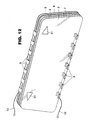
Figure 8 depicts a perspective view of an
electrochromic mirror constructed with an on demand
display.
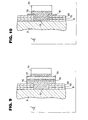
Figure 9 depicts a cross-sectional view of an
electrochromic mirror constructed with an on demand
display using a glass cover sheet over the display
window in the mirror construction.
Figure 10 depicts a cross-sectional view of another
electrochromic mirror constructed with an on demand
display.
Figures 11A, B and C depict the orientation of the
substrates in different constructions of the
electrochromic mirrors and electrochromic devices of
the present invention. Figure 11A depicts a
perpendicular displacement of the first substrate and
the second substrate. Figure 11B depicts a lateral
displacement and a perpendicular displacement of the
first substrate and the second substrate. Figure 11C
depicts an arrangement of the first substrate and the
second substrate, wherein the dimensions of the length
and width of the first substrate are slightly greater
than those of the second substrate. In this
arrangement, the peripheral edge of the first substrate
extends beyond the peripheral edge of the second
substrate.
Figure 12 depicts a perspective view of an
electrochromic mirror constructed with turn signal
indicia.
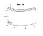
Figure 13 depicts a perspective view of a multi-radius
electrochromic mirror according to the present
invention.
Figures 14A and B depict cross-sectional views of
electrochromic devices, which illustrate different seal
constructions that may be employed in accordance with
the present invention.
Figure 15 is a schematic diagram of a synchronous
manufacturing process for electrochromic mirrors
according to the present invention.
Figure 16 is a schematic diagram of a constant pressure
control system useful for evaporative deposition of
solid electrochromic films.
Figure 17 is a plot of percent transmission versus
wavelength for a continuously variable intensity filter
fixed to the glass of the electrochromic window cell
for voltages applied to the electrochromic medium
within the range of from about 0 volts to about
1.4 volts. In Figure 17, solid curve X represents the
percent transmission versus wavelength (nm) spectrum
for a 600 nm medium-band interference filter having a
bandwidth of about 40 nm. Curve A represents light
transmission through the band pass filter and the
electrochromic window cell with no potential applied.
Curve B represents light transmission through the band
pass filter and the electrochromic window cell at an
applied potential of about 0.3 volts. Curve C
represents light transmission through the band pass
filter and the electrochromic window cell at an applied
potential of about 0.5 volts. Curve D represents light
transmission through the band pass filter and the
electrochromic window cell at an applied potential of
about 0.8 volts. Curve E represents light transmission
through the band pass filter and the electrochromic
window cell at an applied potential of about 1.1 volts.
And curve F represents light transmission through the
band pass filter and the electrochromic window cell at
an applied potential of about 1.4 volts.
The depictions in these figures are for illustrative
purposes only and are not drawn to scale. Unless
otherwise indicated, in the following detailed
description of the invention the element numbers
discussed are descriptive of like elements of all
figures.
DETAILED DESCRIPTION OF THE INVENTION
In accordance with the teaching of the present
invention, there are provided electrochromic mirrors,
such as electrochromic rearview mirrors for a motor
vehicle. These mirrors are constructed from a first
substantially transparent substrate with a
substantially transparent conductive electrode coating
on its inward surface and a second substrate, which may
or may not be substantially transparent, with a
conductive electrode coating, which also may or may not
be substantially transparent, on its inward surface.
Whether the second substrate and the conductive
electrode coating thereon are or are not substantially
transparent will depend on the particular construction
of the mirror.
The first substrate and second substrate may be
positioned in spaced-apart relationship with one
another, being substantially parallel or substantially
tangentially parallel depending upon whether the
substrates are flat or bent. These substrates may also
be laterally displaced from, or in a substantially
flush relationship with, one another. The substrates
may also have respective dimensions such that one of
the substrates is sized and shaped to have a slightly
greater length and width than the other substrate.
Thus, when the substrates are positioned in central
alignment with one another, the peripheral edges of the
slightly larger substrate extend beyond the peripheral
edges of the slightly smaller substrate.
The mirrors have a layer of reflective material coated
either onto (a) the rearmost (non-inward) surface of
the second substrate, where it serves a single role as
a reflective element of the mirror or (b) the inward
surface of the second substrate, where it serves a dual
role as a conductive electrode coating and a reflective
element of the mirror.
In these mirrors, an electrochromic solid film is
coated either onto (a) the transparent conductive
electrode coating of the first substrate, (b) the layer
of reflective material when acting as a conductive
electrode coating on the inward surface of the second
substrate or (c) the substantially transparent
conductive electrode coating on the inward surface of
the second substrate, when the layer of reflective
material is placed on the rearmost (non-inward) surface
of the second substrate.
A sealing means is positioned toward the peripheral
edge of each of the first substrate and the second
substrate to form a cavity, in which is located, either
in a liquid-phase or a solid-phase, an electrolyte
comprising redox reaction promoters and alkali ions
and/or protons. In the cavity, the electrolyte is in
contact with the electrochromic solid film (which
itself is in contact with a conductive electrode
coating on the inward surface of one of either the
first substrate or second substrate) and a conductive
electrode coating (on the inward surface of the other
of the first substrate or second substrate) to form an
electrochromic element.
Finally, a means for introducing an applied potential
to the electrochromic element is also provided to
controllably vary the amount of light reflected from
the mirror.
Decreased light transmissivity in the electrochromic
devices of the present invention (and reflectivity in
the electrochromic mirrors) is primarily provided by
the color-forming reaction that occurs in the
electrochromic solid film. This electrochromic solid
film may be a thin film layer of an inorganic
transition metal oxide. Stoichiometric and
substoichiometric forms of transition metal oxides,
such as Group IV-B, V-B or VI-B oxides like tungsten
oxide, molybdenum oxide, niobium oxide, vanadium oxide,
titanium dioxide and combinations thereof, may be used.
Other conventional inorganic transition metal oxides,
such as those recited in Kamimori III, may also be
employed. Preferably, however, tungsten oxide or doped
tungsten oxide, with suitable dopants including
molybdenum, rhenium, tin, rhodium, indium, bismuth,
barium, titanium, tantalum, niobium, copper, cerium,
lanthanum, zirconium, zinc, nickel, and the like, may
be used as the electrochromic solid film. A beneficial
effect of the addition of the dopant may be to move the
spectral absorption edge of the doped tungsten oxide
coating farther into the visible range of the
electromagnetic spectrum.
Where doped tungsten oxide is used, the dopant should
be present in a concentration within the range of from
about 0.1 % (by mole) to about 20 % (by mole) or even
greater. Preferred doped tungsten oxides include those
where a molybdenum dopant is used within the range of
about 0.5 % (by mole) to about 10 % (by mole).
The electrochromic solid film may be a stack of thin
films, such as a layer of tungsten oxide overcoated
and/or undercoated with a thin film like silicon
dioxide, titanium dioxide, tantalum pentoxide or cerium
oxide. Such overcoats and/or undercoats may help
promote enhanced adhesion of the tungsten oxide
electrochromic solid film to its substrate and/or
passivate it from the electrolyte which it contacts in
the electrochromic element.
When the electrochromic solid film comprises a stack of
thin films, the layers of the multiple layer stack may
individually comprise an electrochromic material. For
example, a stacked electrochromic solid film can be
formed by coating an electrochromic layer of molybdenum
oxide onto a transparent conductor coated substrate (to
a thickness of, for example, about 100 Å to about 3,000
Å), and by overcoating (and/or undercoating) the
molybdenum oxide electrochromic layer with another
electrochromic solid film layer, such as tungsten oxide
having a thickness, for example, in the range of about
100 Å to about 5,000 Å. Alternatively, multiple layers
of tungsten oxide and layers of molybdenum oxide can be
used to form a stacked electrochromic solid film.
When evaporating molybdenum oxide, it may be useful to
melt-process the molybdenum oxide powder prior to
evaporation. Since molybdenum oxide melts at about
795°C, molybdenum oxide powder (typically about 100
mesh) may be placed into a suitable high temperature
resistant, inert evaporation crucible (such as an
alumina crucible) and converted to a solid mass by
heating to a temperature within the range of about
850°C to about 900°C for a period of time of about 60
minutes in a high temperature furnace, preferably in an
inert atmosphere such as a nitrogen atmosphere. Since
molybdenum oxide melts at a lower temperature (less
than about 1,000°C) compared to other electrochromic
metal oxides such as tungsten oxide that melt at a
temperature greater than about 1,000°C, molybdenum
oxide (and equivalent lower melting metal oxides) may
be used as a binder for evaporation of high melt
temperature metal oxide powders.
The thickness of the electrochromic solid film may be
within the range of from about 0.05 µm to about 1.0 µm
or greater, with about 0.25 µm to about 0.75 µm being
preferred, and about 0.3 µm to about 0.6 µm being more
preferred.
The electrochromic solid film may have a microstructure
that is amorphous, crystalline, polycrystalline or
combinations thereof. In electrochromic devices where
the occurrence of photochromism is a concern, it may be
desirable for the electrochromic solid film to possess
a microstructure that is at least partially
crystalline. Such a crystalline microstructure is
believed to minimize the photochromic effect, which may
be deleterious to the operation of the electrochromic
devices. It may also be desirable for the
electrochromic solid film to possess a microstructure
that is porous. In this connection, it may be
desirable for the electrochromic solid film, such as
tungsten oxide or doped tungsten oxide, to have a
density of less than about 90 %, preferably less than
about 80 %, of the density of the bulk oxide.
The electrolyte useful in the electrochromic element of
the electrochromic mirrors of the present invention
should comprise redox reaction promoters, and alkali
ions and/or protons. The electrolyte may be in a
liquid-phase or in a solid-phase.
The redox reaction promoters of the electrolyte
comprise two individual species, a metallocene and a
phenothiazine used in combination.
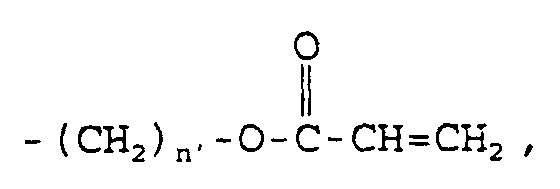
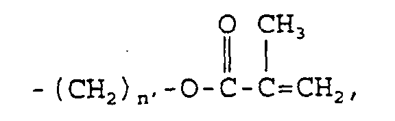
The metallocenes suitable for use as a redox reaction
promoter in the present invention are represented by
the following structure:
wherein R and R
1 may be the same or different, and each
may be selected from the group consisting of H; any
straight- or branched-chain alkyl constituent having
from about 1 carbon atom to about 8 caRbon atoms, such
as CH
3, CH
2CH
3, CH
2CH
2CH
3, CH(CH
3)
2, C(CH
3)
3 and the like;
acetyl; vinyl; allyl; hydroxyl; carboxyl; -(CH
2)
n-OH,
wherein n may be an integer in the range of 1 to about
8; -(CH
2)
n-COOR
2, wherein n may be an integer in the
range of 1 to about 8 and R
2 may be any straight- or
branched-chain alkyl constituent having from about 1
carbon atom to about 8 carbon atoms, hydrogen, lithium,
sodium,
wherein n' may be an
integer in the range of 2 to about 8, or
wherein n' may be an integer in the
range of 2 to about 8; -(CH
2)
n-OR
3, wherein n may be an
integer in the range of 1 to about 8 and R
3 may be any
straight- or branched-chain alkyl constituent having
from about 1 carbon atom to about 8 carbon atoms,
and
or - (CH
2)
n-N
+(CH
3)
3 X
-, wherein n
may be an integer in the range of 1 to about 8 and X
may be Cl
-, Br
-, I
-, ClO
4 - or BF
4 -; and
M
e is Fe, Ni, Ru, Co, Ti, Cr and the like.
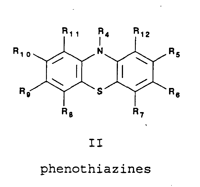
The phenothiazines suitable for use as a redox reaction
promoter in the present invention include, but are not
limited to, those represented by the following
structure:
wherein R
4 may be selected from the group consisting of
H; any straight- or branched-chain alkyl constituent
having from about 1 carbon atom to about 10 carbon
atoms; phenyl; benzyl; -(CH
2)
2-CN; -(CH
2)
2-COOH;
wherein n' may be an
integer in the range of 2 to about 8;
wherein R
2 may be any straight- or branched-chain alkyl
constituent having from about 1 carbon atom to about 8
carbon atoms; and
R
5, R
6, R
7, R
8, R
9, R
10, R
11, R
12 may be selected
from H, Cl, Br, CF
3, CH
3, NO
2, COOH, SCH
3, OCH
3, O
2CCH
3 or
and
R
4 and R
12, when taken together, form a ring
with six atoms (five of which being carbon) having
a carbonyl substituent on one of the carbon atoms.
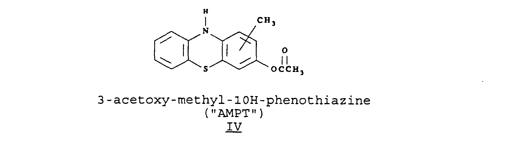
Preferred among phenothiazines
II is phenothiazine
III
as depicted in the following structure:
Other desirable phenothiazines
II include:
An example of a desirable quinone for use as a redox
promoter in the present invention is
Combinations of redox reaction promoters may be
selectively chosen to achieve a desired substantially
non-spectral selectivity when the electrochromic
element (and the mirror in which the electrochromic
element is to function) is dimmed to a colored state.
The redox reaction promoters may be present in the
electrolyte in a total concentration of about 0.005 M
to about 0.5 M, with a total concentration of about
0.02 M to about 0.1 M being preferred. The ratio of
this combination (i.e., total metallocene to total
phenothiazine) should be within the range of about 1:1
to about 1:10, with a preferred combination of redox
reaction promoters being ferrocene and phenothiazine
(III) in about a 1:2 (by mole) to about a 1:4 (by mole)
ratio and, more preferably, having a total
concentration of about 0.07 M to about 0.09 M.
A source of alkali ions may also be included in the
electrolyte. Suitable sources of alkali ions are
lithium salts, such as lithium perchlorate ("LiClO4"),
lithium tetrafluoroborate ("LiBF4"), lithium iodide
("LI"), lithium hexafluorophosphate ("LiPF6"), lithium
hexafluoroarsenate ("LiAsF6"), lithium styrylsulfonate
("LiSS"), lithium triflate ("LiCF3SO3"), lithium
methacrylate, lithium halides other than LI, such as
lithium chloride ("LiCl"), lithium bromide ("LiBr") and
the like, lithium trifluoroacetate ("CF3COOLi") and
combinations thereof. Of these, LiClO4 or combinations
of LiClO4 and LiBF4 are preferred. These sources of
alkali ions may be present in the electrolyte in a
concentration of about 0.01 M to about 1.0 M, with a
concentration of about 0.05 M to about 0.1 M being
preferred.
A source of protons may also be included in the
electrolyte, by, for example, incorporating into the
electrolyte water [for example, in a concentration of
less than about 5 % (v/v), preferably in a
concentration within the range of about 0.5 % (v/v) to
about 2 % (v/v)], or by incorporating into the
electrolyte organic acids, inorganic acids or other
protonic sources suitable for use in conjunction with
organic solvents as are known in the art.
The electrolyte itself may be in a liquid-phase or a
solid-phase, however, where the electrolyte is in a
liquid-phase, a suitable solvent for use in the
electrolyte may solubilize the redox reaction promoters
and alkali ions (and other optional components such as
ultraviolet stabilizing agents which absorb and/or
screen ultraviolet radiation) while remaining
substantially inert thereto (as well as to any other
optional components in the electrolyte). Any material
that remains in its liquid form over the range of
temperatures to which the devices manufactured with the
electrolytes of the present invention will likely be
subjected is suitable for use as a solvent in a liquid-phase
electrolyte [for a non-exhaustive recitation of
such solvents, see e.g., Varaprasad I and Varaprasad
III]. Practically speaking, the solvent may be an
organic solvent, preferably a substantially non-aqueous
organic solvent, which is stable to electrolysis and
other phenomena likely to be encountered during the
practice of this invention.
Suitable solvents may be selected from acetonitrile,
3-hydroxypropionitrile, methoxypropionitrile,
3-ethoxypropionitrile, 2-acetylbutyrolactone, propylene
carbonate, ethylene carbonate, glycerine carbonate,
tetramethylene sulfone, cyanoethyl sucrose,
γ-butyrolactone, 2-methylglutaronitrile,
N,N'-dimethylformamide, 3-methylsulfolane,
glutaronitrile, 3,3'-oxydipropionitrile, methylethyl
ketone, cyclopentanone, cyclohexanone, benzoyl acetone,
4-hydroxy-4-methyl-2-pentanone, acetophenone,
2-methoxyethyl ether, triethylene glycol dimethyl
ether, 4-ethenyl-1,3-dioxalane-2-one, 1,2-butylene
carbonate, glycidyl ether carbonates (such as those
commercially available from Texaco Chemical Company,
Austin, Texas) and combinations thereof, preferred of
which include propylene carbonate, 1,2-butylene
carbonate, the combination of tetramethylene sulfone
and propylene carbonate and the combination of 1,2-butylene
carbonate and propylene carbonate.
Where the electrolyte of the present invention is
desirably a solid-phase electrolyte, a formulation of
starting components may be in situ transformed such as
by polymerization reaction through, for instance,
exposure to ultraviolet radiation or application of
thermal energy, to produce a solid electrolyte. In the
context of ultraviolet radiation activated
polymerization, ultraviolet polymerizable components
[such as those taught by and described in commonly
assigned co-pending United States patent application
Serial Nos. 08/023,675, filed February 26, 1993 (now
abandoned) ("the '675 application") and 08/193,557,
filed February 8, 1994 ("the '557 application"), the
disclosures of each of which are incorporated herein by
reference] may be used to transform into a solid-phase
electrolyte when exposed to ultraviolet radiation.
Other components may also be added to the electrolyte,
with such components preferably being in solution in
liquid-phase electrolytes. These components may
include, but are not limited to, ultraviolet
stabilizing agents, infrared radiation reducing agents,
color tinting agents (e.g., dyes or colorants) and
combinations thereof. Suitable ultraviolet stabilizing
agents and color tinting agents are recited in Lynam
III, the disclosure of which is hereby incorporated
herein by reference. For example, a blue-colored dye
of the phthalocyanine-type, such as "NEOPEN" 808
(commercially available from BASF Corp., Parsippany,
New Jersey), may be added to the electrolyte as a color
tinting agent.
Because many redox reaction promoters show a
substantial absorbance in the ultraviolet region of the
electromagnetic spectrum from about 250 nm to about 350
nm and the electrochromic solid film itself may be
deleteriously affected by exposure to ultraviolet
radiation, it is often desirable to shield the redox
reaction promoters and electrochromic solid film from
ultraviolet radiation. Thus, by introducing an
ultraviolet stabilizing agent to the electrolyte, or
using a solvent which itself acts to absorb ultraviolet
radiation, the lifetime of the electrochromic device
may be extended. It may be particularly advantageous
to include ultraviolet stabilizing agents in the
electrolyte for electrochromic mirrors and
electrochromic devices whose intended use may result in
exposure to outdoor weathering conditions, such as that
encountered by the exterior of a motor vehicle.
Although many materials known to absorb ultraviolet
radiation may be employed herein, preferred ultraviolet
stabilizing agents include "UVINUL" 400 [2,4-dihydroxybenzophenone
(manufactured by BASF Corp., Wyandotte,
Michigan)], "UVINUL" D 49 [2,2'-dihydroxy-4,4'-dimethoxybenzophenone
(BASF Corp.)], "UVINUL" N 35
[ethyl-2-cyano-3,3-diphenylacrylate (BASF Corp.)],
"UVINUL" N 539 [2-ethyl hexyl-2-cyano-3,3'-diphenylacrylate
(BASF Corp.)], "UVINUL" M 40 [2-hydroxy-4-methoxybenzophenone
(BASF Corp.)], "UVINUL" M
408 [2-hydroxy-4-octoxy-benzophenone (BASF Corp.)],
"TINUVIN" P [2-(2H-benzotriazole-2-yl)-4-methylphenyl
(manufactured by Ciba Geigy Corp., Hawthorne, New
York)], "TINUVIN" 327 [2-(3',5'-di-t-butyl-2'-hydroxyphenyl)-5-chloro-benzotriazole
(Ciba Geigy
Corp.)], "TINUVIN" 328 [2-(3',5'-di-n-pentyl-2'-hydroxyphenyl)-benzotriazole
(Ciba Geigy Corp.)],
"CYASORB" UV 24 [2,2'-dihydroxy-4-methoxy-benzophenone
(manufactured by American Cyanamid Co., Wayne, New
Jersey)] and combinations thereof, where a suitable
range of the ultraviolet stabilizing agents is from
about 0.2 % (w/v) to about 40 % (w/v), with about 5 %
(w/v) to about 15 % (w/v) being preferred. The
ultraviolet stabilizing agent should be chosen with an
eye toward avoiding an adverse affect on performance
and electrolyte function.
In addition, ultraviolet absorbing interlayers may be
coated onto, or adhered to, the first substrate and/or
second substrate, particularly the first substrate, to
assist in shielding the electrochromic element from the
degradative effect of ultraviolet radiation. Suitable
ultraviolet absorbing interlayers include those recited
in Lynam III.
Moreover, to assist in extending the lifetime of the
electrochromic device, the electrochromic solid film
may be placed onto the inward surface of the second
substrate -- i.e., coated onto either the reflective
element or the substantially transparent conductive
electrode coating depending on the particular
construction. Location of the electrochromic solid
film on the inward surface of the second substrate may
be desirable where an electrochromic rearview mirror
suitable for use on the exterior of a motor vehicle is
intended to be exposed to outdoor weathering, including
exposure to ultraviolet radiation.
It may also be desirable to employ ultraviolet
absorbing glass or laminates thereof for the first
substrate or for the second substrate in an
electrochromic mirror, particularly for the first
substrate, or for the first substrate and/or the second
substrate in an electrochromic device. Suitable
ultraviolet absorbing glass include that which is
recited in Lynam IV. In addition, it may be desirable
to employ tin oxide, doped tin oxide, zinc oxide or
doped zinc oxide as a substantially transparent
conductive electrode coating on the inward surface of
the first substrate, ultraviolet stabilizing agents in
the electrolyte, ultraviolet absorbing interlayers,
ultraviolet absorbing glass and combinations thereof in
conjunction with positioning the electrochromic solid
film on the inward surface of the second substrate.
Such constructions, particularly with additional
ultraviolet stabilizing agents included in the
electrolyte as described supra, facilitate screening
and/or absorption of ultraviolet radiation by the
components used in the electrochromic mirror or
electrochromic device, including the first substrate,
the conductive electrode coating thereon, and the
electrolyte and its components that are positioned
effectively in front of the potentially ultraviolet
sensitive electrochromic solid film.
Addition of ultraviolet stabilizing agents may be
particularly advantageous when the electrochromic solid
film 7 is coated onto conductive electrode 4' on the
inward surface of substrate 3. (See Figure 5.) In
this construction, the ultraviolet stabilizing agents
may act to screen and/or absorb incident ultraviolet
radiation before it reaches the electrochromic solid
film 7. By so doing, the chance of irradiating the
potentially photochromic or otherwise ultraviolet
radiation vulnerable electrochromic solid film 7 may be
reduced or even substantially eliminated. In contrast,
when coated onto substantially transparent conductive
electrode 4 on the inward surface of substrate 2 (see
Figure 4), the electrochromic solid film 7 may be
directly irradiated by any incident ultraviolet light
that passes through substrate 2. The ultraviolet
screening and/or absorbing affect of the electrolyte,
which in this construction is now positioned behind the
electrochromic solid film 7, has less of an opportunity
to shield the electrochromic solid film 7 from incident
ultraviolet light (although the electrolyte may
effectively absorb any ultraviolet light which is
reflected from the reflective element on substrate 3).
Those of ordinary skill in the art may make appropriate
choices among the various materials available as
described herein for the substrates, coatings,
electrochromic solid films and electrolyte components
-- e.g., redox reaction promoters, sources of alkali
ions and/or protons, solvents, and other components --
to prepare electrochromic mirrors and electrochromic
devices capable of generating a substantially non-spectral
selective gray color suitable for the desired
application. In addiTion, while glass is a suitable
choice of material from which the substrates may be
constructed, other materials may be used, such as
optical plastics like acrylic, polycarbonate,
polystyrene and allyl diglycol carbonate (commercially
available from Pittsburgh Plastic Glass Industries,
Pittsburgh, Pennsylvania under the tradename "CR-39").
Reference to the figures will now be made in order to
more faithfully describe the electrochromic devices,
particularly the electrochromic mirrors, of the present
invention.
With reference to Figures 3A, 3B and 4, it may be seen
that the electrochromic element 1 includes a front
substrate 2 and a rear substrate 3, each of which is
typically glass. However, as described in detail
hereinafter, in certain mirror constructions only the
front or first substrate 2 needs to be at least
substantially transparent, and in those constructions
the rear or second substrate 3 need not be transparent
at all. (See Figure 5.) In fact, substrate 3 may be a
polished metal plate, a metal-coated glass substrate or
a conductive ceramic material.
By convention, the first substrate 2 (the frontmost or
outermost substrate) is the substrate of the
electrochromic device positioned closest to any
principal source of incoming or incident
electromagnetic radiation and, in an electrochromic
mirror, the second substrate 3 is the substrate onto
which a layer of reflective material 8 is coated. Put
another way, the first substrate 2 is the substrate
into which a driver of or passenger in a motor vehicle
may first look through to view an image. In an
electrochromic device, such as a glazing, a window or a
sun roof for a motor vehicle, the first substrate 2 is
the substrate exposed directly to, and often in contact
with, the outdoor environment and is exposed directly
to solar ultraviolet radiation.
Substrates 2,3 should be positioned substantially
parallel to one another if planar (or positioned
substantially tangentially parallel to one another if
bent), or as close to parallel (or tangentially
parallel) to one another as possible so as to minimize
image separation which may lead to double imaging.
Double imaging is particularly noticeable when mirrors
are colored to a dimmed state. Double imaging may be
further minimized in mirror constructions as described
hereinafter.
Onto each of the inward surfaces of substrates 2,3 is
coated a conductive electrode coating 4 or 4'. The
conductive electrode coatings 4,4' may be constructed
from the same material or different materials,
including transparent electronic conductors, such as
tin oxide; indium tin oxide ("ITO"); half-wave indium
tin oxide ("HW-ITO"); full-wave indium tin oxide ("FW-ITO");
doped tin oxides, such as antimony-doped tin
oxide and fluorine-doped tin oxide; doped zinc oxides,
such as antimony-doped zinc oxide and aluminum-doped
zinc oxide, with tin oxide, doped tin oxide, zinc oxide
or doped zinc oxide being preferred where long-term
ultraviolet resilience is desired in the device.
In certain mirror constructions, the conductive
electrode coating 4' need not be substantially
transparent. Rather, the layer of reflective material
that serves as the reflective element of the mirror
(with any other coatings used to form a thin film
stack) may also serve as conductive electrode coating
4', thereby allowing a potential to be applied to the
electrochromic element 1. Suitable materials for this
layer of reflective material include metals, such as
aluminum, palladium, platinum, titanium, chromium,
silver, nickel-based alloys and stainless steel, with a
high reflector (having a reflectance greater than about
70 %), like silver or aluminum, being preferred.
However, where resistance to scratching and
environmental degradation is a concern, a medium
reflector (having a reflectance within the range of
about 40 % to about 70 %), like chromium, stainless
steel, titanium and nickel-based alloys, is preferred.
As an alternative to the use of these metals as a
reflective element, multi-coated thin film stacks of
inorganic oxides, halides, nitrides or the like, or a
thin film layer of high index material may also be
used.
The conductive electrode coatings 4,4' may be thin
films of metal, such as silver, aluminum and the like,
with a thickness of less than about 200 Å, which may be
as low as less than about 100 Å, so that the conductive
electrode coatings 4,4' are sufficiently conductive yet
sufficiently transmissive. It may be desirable to
index match a thin film of metal through the use of a
thin film layer of a transparent metal oxide, metal
nitride, metal halide or the like, such as indium
oxide, zinc oxide, tin oxide, magnesium fluoride,
titanium nitride, silicon dioxide, tungsten oxide or
titanium dioxide, either as an overcoat or an undercoat
to the thin film of metal to assist in reducing its
reflectance, and increasing its transmittance, of
incident visible light [see e.g., commonly assigned
United States Patent 5,239,406 (Lynam) ("Lynam VI")].
For example, a layer of a metal, such as silver,
preferably having a thickness of less than about 200 Å
and a sheet resistance of less than about 12 ohms per
square (more preferably, less than about 10 ohms per
square, and most preferably, less than about 8 ohms per
square), may be overcoated with a metal oxide
transparent conductor [such as a thin film layer of
indium oxide (itself either undoped or doped with tin
to form indium tin oxide)] and/or undercoated with a
metal oxide layer [such as a thin film layer of indium
oxide (itself either undoped or doped with tin to form
indium tin oxide)] to form a substantially transmitting
multi-layer transparent conductor on a glass surface.
The sheet resistance of the multi-layer transparent
conducting stack is preferably less than about 10 ohms
per square, more preferably less than about 8 ohms per
square, and most preferably less than 6 ohms per
square. The transmission of visible light through the
multi-layer transparent conductor coated glass
substrate (which ordinarily comprises glass/metal
oxide/metal/metal oxide or glass/metal/metal oxide such
that the outermost metal oxide layer overcoating the
thin metal layer serves as a barrier coating to reduce
or prevent direct contact between the potentially
electrochemically vulnerable metal layer and any
electroactive medium, such as an electrochemically
active liquid, thickened liquid and the like, that
contacts the multi-layer transparent stack) is
preferably greater than about 70 %, more preferably
greater than about 80 %, and most preferably greater
than about 85 %.
Though silver is a preferred metal in such multi-layer
transparent conducting stacks, aluminum may also be
employed, particularly where the optical design of the
multi-layer stack is optimized to maximize overall
light transmission. Also, the outermost overcoating
metal oxide layer should be at least somewhat, and
preferably significantly, conducting so as not to form
an electrical insulating overcoat on the metal layer.
The sheet resistance for such a metal oxide layer
should be less than about 2,000 ohms per square, with
less than about 1,000 ohms per square being preferred
and less than about 500 ohms per square being more
preferred. This overcoating metal oxide layer may be
any at least partially conducting, substantially
transparent metal oxide such as tin oxide (doped or
undoped), indium oxide (doped or undoped), zinc oxide
(doped or undoped) and cadmium stannate. The thickness
for the overcoating metal oxide layer (as well as the
thickness of any undercoating metal oxide layer) is
preferably less than about 500 Å, more preferably less
than about 300 Å, and most preferably less than about
200 Å.
Such multi-layer transparent conducting stacks are
preferably deposited using in-line sputter deposition
chambers with either planar or rotary magnetron
targets, and with deposition of the metal oxide layers
being achieved either by reactive deposition of an
oxide coating by sputtering from a metal target (or
from a conductive, pressed oxide target) in an oxygen-rich
atmosphere, or by radio-frequency ("RF")
sputtering from an oxide target. An example of a
multi-layer transparent conducting stack is
glass/ITO/Ag/ITO, with the thickness of the ITO layers
being in the range of about 100 to about 300 Å and the
thickness of the silver layer being in the range of
about 80 to about 200 Å.
An economical electrochromic rearview mirror may be
fabricated by using clear glass as a front substrate,
substrate 2, (preferably constructed from float glass)
which is coated on its inwardly facing surface with a
substantially transmitting, multi-layer transparent
conductor comprising at least a thin metal layer
overcoated with a transparent conductor metal oxide.
For instance, a soda-lime glass substrate coated with
indium tin oxide (having a thickness of about 150
Å)/silver (having a thickness of about 150 Å)/indium
tin oxide (having a thickness of about 150 Å) may be
used for the front substrate, substrate 2. The rear
substrate, substrate 3, is coated with a metal
reflector (such as silver, aluminum, chromium,
titanium, nickel-based alloys like Hastelloy, iron-based
alloys like stainless steel, and the like), which
also serves as the electrical conductor on substrate 3.
An electrochromic medium is disposed between the two
confronting inwardly facing conductor surfaces. An
example of such a construction is glass/indium tin
oxide (having a thickness of about 150 Å)/silver
(having a thickness of about 150 Å)/indium tin oxide
(having a thickness of about 150
Å)//electrolyte//tungsten oxide (having a thickness of
about 6,000 Å)/aluminum (having a thickness of about
2,000 Å)/chromium (having a thickness of about 1,000
Å)/glass, which construction is economical to
manufacture as the total thickness of the metal oxide
transparent conducting ITO layer is only about 300 Å.
This total thickness compares favorably to the use of a
half wave or full wave ITO layer with a thickness of
about 1,500 Å or 3,000 Å, respectively.
The sheet resistance of the conductive electrode coated
glass substrates 2,3 should be less than about 100 ohms
per square, with less than about 20 ohms per square
being preferred. (However, as described in greater
detail hereinafter, for reasons of economy it may
sometimes be preferable to use substantially
transparent conductive electrodes having a sheet
resistance of greater than about 20 ohms per square.)
Conductive electrode coated glass substrates are
available commercially. For instance, ITO-coated glass
substrates made from a glass substrate having deposited
thereon a conductive coating of indium oxide that has
been doped with tin oxide may be obtained from Donnelly
Corporation, Holland, Michigan. In addition, tin
oxide-coated glass substrates, known as "TEC-Glass"
products, may be obtained from Libbey-Owens-Ford Co.,
LOF Glass Division, Toledo, Ohio.
The "TEC-Glass" products are manufactured by an on-line
chemical vapor deposition process. This process
pyrolytically deposits onto clear float glass a multi-layer
thin film structure, which includes a
microscopically thin coating of fluorine-doped tin
oxide (having a fine grain uniform structure) with
additional undercoating thin film layers disposed
between the fluorine-doped tin oxide layer and the
underlying glass substrate. This structure inhibits
reflected color and increases light transmittance. The
resulting "TEC-Glass" product is a non-iridescent glass
structure having a haze within the range of from about
0.1 % to about 5 %; a sheet resistance within the range
of from about 10 to about 1,000 ohms per square or
greater; a daylight transmission within the range of
from about 77 % to about 87 %; a solar transmission
within the range of from about 64 % to about 80 %; and
an infrared reflectance at a wavelength of about 10 µm
within the range of from about 30 % to about 87 %. See
e.g., United States patent application Serial No.
08/061,742, filed May 17, 1993, the disclosure of which
is hereby incorporated herein by reference.
Examples of the "TEC-Glass" products include "TEC 10"
(10 ohms per square sheet resistance), "TEC 12" (12
ohms per square sheet resistance) and "TEC 20" (20 ohms
per square sheet resistance) tin oxide-coated glass.
More specifically, "TEC 10", for instance, is made from
an on-line pyrolytically-coated float glass, onto which
has been coated a fluorine-doped tin oxide layer
containing as an undercoat an anti-iridescence means.
This anti-iridescence means includes a double layer
composed of a layer of silica-silicone deposited onto a
layer of tin oxide.
The specific resistivity of the conductive electrode
coatings 4,4' useful in the present invention may be
between about 5 x 10⁻³ to about 1 x 10⁻⁶ ohm.centimeter,
depending on the material from which the conductive
electrode coatings 4,4' are constructed, and on the
method of deposition and formation of the conductive
electrode coatings 4,4'. For instance, where the
conductive electrode coatings 4,4' are ITO, the
specific resistivity is typically within the range of
about 1 x 10⁻⁴ to about 3 x 10⁻⁴ ohm.centimeter. And
where the conductive electrode coatings 4,4' are doped
tin oxide, the specific resistivity is typically within
the range of about 3 x 10⁻⁴ to about 5 x 10⁻³
ohm.centimeter. Where the conductive electrode coating
4' is a metal, the specific resistivity is typically
less than about 5 x 10⁻⁵ ohm.centimeter. And where the
conductive electrode coating 4' is silver, the specific
resistivity is typically less than about 3 x 10⁻⁵
ohm.centimeter. The thickness of the metal should be
such that the sheet resistance of conductive electrode
coating 4' is less than about 0.75 ohms per square,
preferably less than about 0.5 ohms per square and more
preferably less than about 0.25 ohms per square.
Preferably, the thickness of the metal used for
conductive electrode coating 4' should be within the
range of about 200 Å to about 5,000 Å, with a thickness
within the range of 500 Å to about 2,500 Å being
preferred and a thickness within the range of about
750 Å to about 1,500 Å being most preferred.
The substantially transparent conductive electrode
coating 4 on the inward surface of substrate 2 is
preferably highly transmissive in the visible spectrum;
that is, with a light transmittance within the range of
at least about 60 % to greater than about 80 %.
Likewise, when the conductive electrode coating 4' on
the inward surface of substrate 3 is to be highly
transmissive, similar high light transmittance is
desirable.
The conductive electrode coatings 4,4' should also be
highly and uniformly conductive in each direction to
provide a substantially uniform response when a
potential is applied to the electrochromic element 1.
And, the conductive electrode coatings 4,4' should be
inert (physically, chemically and electrochemically
inert) to the constituents of the electrochromic solid
film 7 and the electrolyte 6.
Where the electrochromic solid film 7 is deposited as a
coating onto the inward surface of either of conductive
electrode coated glass substrates 2,3, it is a barrier
coating between whichever of the conductive electrode
coatings 4,4' it is deposited on and the electrolyte 6,
as well as a barrier coating between the conductive
electrode coatings 4,4' themselves.
The electrochromic solid film 7 may be deposited using
a variety of film deposition means including, but not
limited to, vacuum deposition techniques, such as
thermal evaporation, electron beam evaporation, sputter
deposition, ion plating, laser-assisted deposition,
microwave-assisted deposition and ion-assisted
deposition; thermal spraying; pyrolytic deposition;
chemical vapor deposition ("CVD"), including
atmospheric CVD, plasma enhanced CVD, low pressure CVD
and the like; wet chemical deposition, including dip
coating, spin coating and spray coating; and thick film
methods such as those used in the application of pastes
and inks. Suitable deposition results may be obtained
with wet chemical deposition as taught by and described
in United States Patents 4,855,161 (Moser); 4,959,247
(Moser); 4,996,083 (Moser); 5,252,354 (Cronin) and
5,277,986 (Cronin), the disclosures of each of which
are hereby incorporated herein by reference.
It may be beneficial to deposit the electrochromic
solid film using vacuum deposition, preferably with an
electron beam evaporation technique where the
electrochromic solid film 7 is tungsten oxide and is to
be placed in direct contact with, or deposited (for
example, with an alternate evaporation filament,
crucible, boat or an alternate electron beam gun
assembly, or the like) as a layer on, the inward
surface of substrate 3, which is already coated with a
layer of reflective material that serves the dual role
as a reflective element and a conductive electrode
coating 4'.
The layer of reflective material, which also serves as
a conductive electrode coating 4', with or without any
adhesion enhancing undercoat layers (discussed
hereinafter), may be deposited on the inward surface of
substrate 3, with tungsten oxide deposited as an
overcoat, without the need to refixture, break vacuum
or the like. Thus, it is seen that such a dual purpose
reflective element may be deposited with manufacturing
ease and economy. This is particularly so when
compared with conventional mirror constructions where
the reflective element is coated over the rearmost
(non-inward) surface of a substrate (which itself is
coated with a substantially transparent conductive
electrode coating on the opposite, inward surface) in
one operation, and thereafter loaded into a vacuum
chamber to deposit tungsten oxide onto the other
surface of the substrate, which is coated with a
substantially transparent conductive electrode.
When vacuum depositing the electrochromic solid film 7
by evaporation or the like, a backfill pressure in a
vacuum chamber within the range of about 1 x 10⁻⁴ torr
to greater than about 5 x 10⁻⁴ torr may be used. This
backfill pressure may typically be achieved by
evacuating the vacuum chamber to some lower base
pressure (e.g., less than about 5 x 10⁻⁵ torr) and then
backfilling the vacuum chamber with a gas such as
nitrogen, argon, krypton, oxygen, water vapor and the
like, or combinations thereof, to elevate the pressure
in the vacuum chamber to a desired backfill pressure.
Alternatively, the vacuum chamber may be pumped from
atmospheric pressure down to about a pressure within
the range of about 1 x 10⁻⁴ torr to greater than about
5 x 10⁻⁴ torr, and tungsten oxide, for instance, may
then be evaporated onto the desired surface of
substrates 2,3. It may be desirable during such vacuum
deposition to monitor and to control the pressure
within the vacuum chamber using pumps, valves and
closed loop controls as is known in the vacuum
deposition art.
It may be useful to maintain a relatively constant
backfill gas pressure during evaporative deposition of
the inorganic oxide solid electrochromic film layer, or
of other layers such as an adhesion promoter layer and
a reflector layer. For example, when evaporating
tungsten oxide in the presence of a backfill gas
pressure at a desired set backfill pressure, it is
usually desirable to first pump the chamber from
atmospheric pressure to a base pressure of about 0.1
times the desired backfill pressure. By so doing, the
backfill pressure should remain constant during
deposition and not be perturbed by outgasing from
chamber walls, fixtures and the like.
In order to achieve a relatively constant backfill
pressure during deposition without expending extra
process and cycle time to pump to 0.1 times the desired
backfill pressure, a constant pressure control system,
as represented in Figure 16, may be used. Here, the
pressure in vacuum chamber 1600 is monitored by
pressure transducer 1601 whose output signal is
compared to a pressure set point VPS at the input of
differential amplifier/gas controller 1602. The output
1603 of differential amplifier/gas controller 1602 is
used to operate variable valve 1604 which will admit
gas from gas source 1605 to the vacuum chamber so that
the difference between the pressure transducer 1601
output and the pressure set point VPS remains constant.
The backfill pressure in the chamber is principally
established by gas admittance through fixed valve 1606.
The closed-loop operation of variable valve 1604, as
described above, serves to decrease the volume of
backfill gas admitted when the chamber pressure (as
detected by pressure transducer 1601) is determined to
rise due to outgasing of water vapor and other gaseous
species from the chamber walls, fixtures, evaporant,
etc., and to increase admittance of backfill gas again
when chamber pumping decreases the partial pressure of
outgassed species so as to maintain a constant backfill
pressure in the chamber during evaporation.
With reference to Figure 4, the conductive electrode
coatings 4,4' in the mirror construction so depicted
are substantially transparent. Likewise, in the mirror
construction depicted in Figure 7, conductive electrode
coatings 4,4' and substrate 3 are substantially
transparent.
With reference to Figure 5, however, only the
conductive electrode coating 4 of the first substrate 2
in the mirror construction so depicted need be
substantially transparent; that is, the conductive
electrode coating 4' need not be substantially
transparent. In addition, the second substrate 3 need
not be substantially transparent. In this aspect of
the present invention, the layer of reflective material
may be coated directly onto the inward surface of the
second substrate 3 to serve as the conductive electrode
coating 4' as well.
Onto one of conductive electrode coatings 4,4' is
deposited a coating of an electrochromic solid film 7,
such as an inorganic transition metal oxide, like
tungsten oxide. As noted herein, where photochromism
may be a concern, the electrochromic solid film 7
should be positioned at the inward surface of substrate
3 (which surface is coated with conductive electrode
coating 4'). By so doing, the electrochromic solid
film 7 should benefit from the ultraviolet screening
and/or absorbing capabilities of the components of the
mirror positioned in front of it and closer to incident
light.
Silver or aluminum are suitable choices for conductive
electrode coating 4' of substrate 3 because either
metal may serve as a reflective element for the mirror
and metal coatings in general are significantly more
conductive than semiconducting oxides, such as ITO or
doped tin oxide. As a consequence of using a thin film
of metal as conductive electrode coating 4', the
substantially transparent conductive electrode coating
4 of substrate 2 may be chosen with an eye toward
higher sheet resistance, such as, for example, about 40
to about 100 ohms per square. This is desirable
because conductive electrode coatings of higher sheet
resistance are typically thinner and less expensive
than conductive electrode coatings of lower sheet
resistance. ITO or doped tin oxide are suitable
choices for substantially transparent conductive
electrode coating 4 used in conjunction with a thin
film of metal as a reflective element, such as silver
or aluminum, that is to serve as conductive electrode
coating 4'. In addition, the use of such a thin film
of metal as conductive electrode coating 4' permits the
conductive strip or clip connectors (known as "bus
bars") to be reduced in length, even to a point
contact, on conductive electrode coating 4', rather
than being used about a substantial portion of the
periphery. That is, bus bars 9 may be attached at only
a portion of the thin film of metal and still apply an
adequate potential across the conductive electrode
coatings 4,4'.
Moreover, use of the reflective element of the mirror
as the conductive electrode coating 4' is also
appealing from a production standpoint. Such use
reduces material and manufacturing costs since an
additional electrode layer or reflective element need
not be provided. In addition, this dual purpose
reflective element/conductive electrode coating is
environmentally appealing because it is no longer
necessary to enhance resistance to degradation, such as
environmental degradation, by applying a paint
overcoat, which may be lead-based. In addition, such
conventional reflective elements located on the
rearmost surface of the mirror construction are
typically opaque, and, as described hereinafter, such
opacity may result in additional manufacturing effort
should an "on demand display" be desirable in a
particular mirror construction.
Between the layer of reflective material, typically
silver, and the surface of substrate 3 to which it is
applied, may desirably be coated a thin film adhesion
enhancing means to act as an adhesion promoter
("adhesion promoter"). (See Figure 6.) The adhesion
promoter 11 enhances long-term adhesion of the layer of
reflective material to the surface of substrate 3. It
is known in the art that there are certain difficulties
in adhering a reflective material such as silver to a
substrate such as glass, especially where the
reflective material is to be deposited by a vacuum
deposition process such as evaporation. The adhesion
promoter 11 of the present invention overcomes these
difficulties and provides a practical way of applying a
coating which will function as a dual purpose
reflective element/conductive electrode in an
electrochromic mirror.
Suitable adhesion promoters 11 include thin films of
metal and metal oxides that provide enhanced adhesion
over a silver to glass interface, such as chromium,
stainless steel, nickel-based alloys (e.g., Hastelloy),
titanium, monel, nichrome, molybdenum, metal oxides
(e.g., silver oxide, aluminum oxide, indium oxide,
indium tin oxide, tin oxide, doped tin oxide, zinc
oxide, doped zinc oxide and chromium oxide) and the
like. The use of thin films of metal or conducting
metal oxides (such as indium tin oxide and doped tin
oxides) as adhesion promoters as described herein is
advantageous in view of their low cost (due to the
relative simplicity of evaporating metal onto a surface
of a substrate to form metal or metal oxide coatings),
their electrical conductivity that augments that of
conductive electrode coating 4', and their mechanical
hardness. In addition, use of such thin films of metal
or conducting metal oxides as adhesion promoters which
undercoat the layer of reflective material assist in
maintaining the conductivity of the bus bars 9. This
is particularly advantageous in the event a bus bar
(e.g., a clip connector) should pierce through the
layer of reflective material, because the adhesion
promoter is a conductive material that sustains
electrical continuity.
An adhesion promoter 11 may be an undercoat of a thin
film of a single metal, a metal oxide, or a combination
of a metal and a metal oxide. A method for promoting
adhesion of the layer of reflective material to a
surface of substrate 3 involves deposition, such as by
vacuum evaporation or sputtering of a metal, typically
silver, initially in an oxygen-rich atmosphere. In
this atmosphere, a thin film of silver oxide is applied
onto a surface of substrate 3. Then, by progressively
decreasing the oxygen atmosphere to zero, a
progressively decreased amount of oxide is formed with
respect to the metal content in the thin film deposited
on the substrate 3. Finally, with little to no oxygen
remaining in the atmosphere, a thin film of silver may
be built-up upon the previously formed undercoat of its
own oxide/gradient oxide to form an adhesion-promoting
layer between the surface of substrate 3 and the layer
of reflective material. Likewise, chromium may be
deposited initially as a thin film of chromium oxide in
an atmosphere of enhanced partial pressure of oxygen,
followed by deposition of a thin film of metallic
chromium by depleting the supply of oxygen. Oxygen may
be introduced again to permit the deposition of silver
oxide, and finally with deposition of a thin film of
metallic silver following in an inert atmosphere. The
substrate may also be heated, such as to a temperature
within the range of from about 100°C to about 500°C
(and preferably within the range of from about 150°C to
about 400°C), during reactive deposition of metal to
form a metal oxide. Heating the substrate in this
manner may assist reactive formation of the oxide from
the metal and may further enhance adhesion. Moreover,
a metal oxide, such as chromium oxide, silver oxide,
aluminum oxide, indium oxide, tin oxide, titanium oxide
or tantalum oxide, may be deposited, such as reactively
deposited in an oxygen-rich atmosphere, by vacuum
deposition (e.g., evaporation to sputtering) to form
adhesion promoter 11.
The adhesion promoter 11 should have a thickness within
the range of from about 10 Å to about 2,500 Å or
greater, with about 50 Å to 1,000 Å being preferred.
Adhesion promoter 11 can be a single thin film coating
or a stack of thin film coatings. For example, the
inward facing surface of substrate 3 can first be
coated with a conducting metal oxide adhesion promoter
coating of indium tin oxide, which in turn is
overcoated with a metal adhesion promoter coating of
chromium, with this stack in turn being overcoated with
a reflective coating of silver.
In addition to mirrors employing an electrochromic
solid film, adhesion promoter 11 of the present
invention may also be used in mirrors employing other
types of electrochromic technology, such as
electrochromic solution technology of the
electrochemichromic type (e.g., Byker I, Byker II,
Varaprasad I and Varaprasad III). Thus, adhesion
promoter 11 may be used to construct electrochromic
mirrors containing an electrochromic solution in which
a single coating or stack of coatings functions as a
dual purpose reflective element/conductive electrode.
For some applications, it may be desirable to prevent
build-up of deposited materials (such as, tungsten
oxide and/or silver) at a portion or portions of the
inward surface of substrates 2 or 3 inboard from an
edge thereof. In this regard, a magnetizable metal
mask may be placed over the portion(s) where it is
desired to prevent build-up of such deposited
materials. The magnetizable metal mask may then be
held at that portion of the substrate under a magnetic
influence while the material is deposited. For
example, a magnetizable metal mask may be placed at the
desired location on the inward surface of substrate 3
prior to coating the inward surface thereof with an
adhesion promoter (e.g. chromium), a layer of
reflective material (e.g., silver) and a layer of an
electrochromic solid film (e.g., tungsten oxide). A
magnet may be placed on the rearmost surface of
substrate 3 behind that location on the inward surface
of substrate 3 to ensure that the mask is held in
place. Upon removal of the mask after completion of
deposition of the chromium/silver/tungsten oxide stack
onto the inward surface of substrate 3, a depositionfree
portion of that surface is formed.
As stated supra, the spaced-apart glass substrates 2,3
have a sealing means 5 positioned therebetween to
assist in defining the interpane spacing in which the
electrochromic solid film 7 and the electrolyte 6 are
located. The sealing means 5 may be constructed of any
material inert (physically, chemically and
electrochemically inert) to the electrochromic solid
film 7 and the components of the electrolyte 6, as well
as to any other material used in the device. To that
end, the sealing means 5 may be chosen from the
following materials including, but not limited to,
various thermosetting materials, such as epoxy resins
and silicones, various thermoplastic materials, such as
plasticized polyvinyl butyral, polyvinyl chloride,
paraffin waxes, ionomer resins, various inorganic
materials and the like. For a further recitation of
suitable sealing materials, see commonly assigned
United States Patent 5,233,461 (Dornan).
The thickness of the sealing means 5 may vary from
about 10 µm to about 1,000 µm. Preferably, however,
this thickness is about 50 µm to about 100 µm.
In addition, the sealing means 5 may prevent escape of
the electrolyte 6, when in a liquid-phase, from the
electrochromic element 1 or penetration of
environmental contaminants into the electrolyte,
whether in a liquid-phase or in a solid-phase. Of
course, when the electrolyte is in a solid-phase,
leakage or seepage of the electrolyte from the mirror
is not a concern, but contamination may be.
Desirably, the sealing means 5 comprises a polymer seal
formed by the cure of a latent cure adhesive
formulation, such as a latent cure epoxy. Such latent
cure adhesive formulations, as known in the adhesives
arts, comprise an adhesive system (for example, a
latent cure epoxy system). A latent cure adhesive
system is sometimes referred to as a one-package system
since it is supplied in an uncured or only partially
cured form in a single package and thus does not
require the mixing together of two or more components
(such as a resin and a separate hardener as is common
with many adhesive systems like two-component epoxy
systems). This obviates the need to mix together two
or more components when forming the sealing means 5.
Latent cure epoxies typically have a relatively long
pot life (e.g., hours to days at room temperature), and
so do not appreciably set up and harden at room
temperature. However, when exposed to an elevated
temperature (which depends on the chosen resin and
latent curing agent and typically, for the preferred
systems used in this present invention, with the
activation temperature being at least about 60°C, and
more preferably at least about 90°C), they cure rapidly
to attain their intended cure and bond strength. Thus,
latent cure epoxies have a temperature of activation,
below which substantial cure is not initiated, but
above which relatively rapid cure is achieved. Such
systems may be advantageously employed as the seal
material in the electrochromic cells of the present
invention. Also, latent cure adhesives are
particularly amenable to commercial scale manufacture
of electrochromic devices such as electrochromic
rearview mirrors (whether by silkscreening or by direct
dispensing from a needle valve dispenser). These
latent cure adhesives have a long pot life so that a
batch of adhesive may be used over many hours of
production with the assurance that the adhesive will
not unduly age due to room temperature cure (which can
lead to inconsistency and potential unreliability in
the seal so formed). These latent cure adhesives allow
for ease and economy of manufacture since by using such
one-package, latent cure systems, silkscreens and
dispenser systems will not become clogged or obstructed
due to room temperature-induced hardening of the seal
adhesive system, and the viscosity of the adhesive
system remains relatively constant throughout the
production day. Clean-up is also facilitated due to a
reduction and near elimination of prematurely hardened
adhesive on silkscreens or within, for instance,
dispenser tubing, needles, and the like.
One-package, latent cure adhesive formulations useful
in forming the sealing means
5 may typically include a
resin (preferably, an epoxy resin such as EPON Resin
828 commercially available from Shell Chemical Company,
Houston, Texas), and a latent curing agent (such as a
dicyandiamide, a modified amine, an organic acid
anhydride, a microencapsulated amine, an epoxide adduct
encapsulated in a polymerized polyfunctional epoxide,
and an adipic dihydrazide). Latent curing agents are
commercially available, such as from Air Products and
Chemicals Incorporated, Allentown, Pennsylvania under
the tradenames ANCAMINE® 2014AS and ANCAMINE® 2014FG.
These latent curing agents are modified amines. Other
latent curing agents, such as imidazole-based systems,
may also be used. These imidazole-based latent curing
agents are also commercially available from Air
Products and Chemicals Incorporated under the
tradenames IMCURE® (such as, IMCURE® AMI-2) and
CUREZOL™ (such as, CUREZOL™ 2E4MZ, 1B2MZ, 2PZ, C17Z,
2MZ Azine, 2PHZ-5 and 2MA-OK). Also, latent curing
agents are commercially available from AJINOMOTO
Incorporated, Teaneck, New Jersey under the tradename
AJICURE® , examples of which include AJICURE® PN-23 and
AJICURE® MY-24. Latent cure adhesives, such as latent
cure epoxies, optionally and desirably, include fillers
(such as, silica-based fillers like IMSIL A-8, which is
commercially available from UNIM Specialty Minerals
Incorporated, Elco, Illinois, and calcium carbonate-based
fillers like SS-14066 HUBERCARB OPTIFILL, which
is commercially available from J.M. Huber Corporation,
Quincy, Illinois), and coupling agents (useful as
adhesion promoters) like the silane coupling agents
listed in Table I below:
| SILANE/ COMMERCIAL SUPPLIER | CHEMICAL NAME |
| Z6020, Dow Corning | N-(2-aminoethyl)-3-amino-propyltrimethoxy silane |
| Z6032, Dow Corning | N-[2-vinyl benzylamino-ethyl]-3-aminopropyltrimethoxy silane |
| Z6076, Dow Corning | 3-chloropropyltrimethoxy silane |
| A187, Union Carbide | γ-glycidoxypropyltrimethoxy silane |
| A1100, Union Carbide | γ-aminopropyltriethoxy silane |
| A174, Union Carbide | γ-methacryloxypropyltrimethoxy silane |
| Aldrich Chemicals | 2-dichloropropyltrimethoxy silane |
| Aldrich Chemicals | diphenyldiethoxy silane |
| Q1-6101. Dow Corning | proprietary organic trimethoxy silane |
Coloring agents (such as, carbon black and heavy metal-or
iron-based pigments) and spacer beads (such as,
glass) may also be included. A particularly useful
latent cure adhesive formulation for the commercial
production of electrochromic rearview mirrors with good
manufacturing economics and with excellent double image
performance exhibited by the mated substrates
comprises:
| Component | Type | Pans Per Hundred Parts of Resin | Type |
| Resin | EPON 8281 | - | Epoxy |
| Latent Curing Agent | ANCAMINE® 2014FG | 28 | Modified Amine |
| Filler | Calcium Carbonate | | 30 |
| Coloring Agent | Carbon Black | | 1 |
| Spacer Beads | Glass | | 1 |
This latent-cure adhesive formulation may either be
silkscreened to form the sealing means 5 or may be
applied using an automatic fluid dispensing system,
such as a high speed, computer controlled fluid
dispensing system supplied by ASYMTEK, Carlsbad,
California under the tradename AUTOMOVE 400, and the
like. Use of a latent curing agent (which produces
long-term stability at room temperature but rapid cure
at elevated temperatures) in the adhesive formulation
used to establish the sealing means 5 is particularly
advantageous when using an automatic fluid dispensing
system. In such a system, constancy and control of the
fluid viscosity is facilitated, and consistency and
precision of the bead of fluid adhesive dispensed
around the perimeter of the substrate is also
facilitated. Latent curing agents are particularly
desirable when precision dispensing valves are used,
such as a rotary positive displacement ("RPD") valve
like the DV-06 valve commercially available from
ASYMTEK.
Once the latent cure adhesive is screened or dispensed
around the edge perimeter of a substrate, and after the
second substrate is juxtaposed therewith to establish a
cell with an interpane spacing, the latent cure
adhesive may be rapidly cured by exposure to elevated
temperatures, typically greater than about 60°C. Epoxy
adhesive systems that use ANCAMINE® latent curing
agents and that are cured by exposure to a temperature
of at least about 110°C for a period of time of about
one hour, or less, perform excellently. What's more,
the cured seal exhibits resilience when exposed to
boiling water for a period of time in excess of 96
hours. The double image performance for such
ANCAMINE® -cured mirror cells was also found to be
superior to comparable two-component epoxy systems in
that, during typical production of electrochromic
rearview mirrors, double imaging measured from cells
using the latent curing agent to effect a cure to form
the sealing means 5 was consistently lower than
comparably processed electrochromic rearview mirrors
which used a two-component epoxy to form the sealing
means 5. Also, the glass transition temperature (Tg)
for the sealing means 5 formed by cure of a one-package,
latent cure adhesive is preferably less than
about 140°C, more preferably less than about 120°C and
most preferably less than about 100°C.
One-package adhesive and sealing systems, that are
supplied with a latent curing agent already
incorporated in the adhesive formulation, are also
commercially available. Such one part curing adhesives
incorporate an integral hardener or catalyst and
typically include a liquid epoxy resin and a
dicyandiamide hardener. Examples include a one part
epoxy adhesive commercially available from Al
Technology, Princeton, New Jersey, under the tradenames
EH7580, ME 7150-SMT or ME 7155-ANC; a one part epoxy
adhesive commercially available from American Cyanamid,
Wayne New Jersey under the tradename CYBOND 4802; and a
one part epoxy commercially available from CHEMREX,
Commerce City, Colorado, under the tradename CHEMREX
7459-9772. Also, one part aerobic adhesive and sealing
systems, which depend on oxygen or moisture in the air
to activate or achieve cure, may also be used to form
the sealing means 5. An example of such a one part
aerobic adhesive and sealing system is moistureactivated
silicone.
Double image performance in rearview mirrors is greatly
assisted by the use of a vacuum-assisted sealing
technique. An example of such a technique is a vacuum
bag technique where, spacer means, such as spacer
beads, are disposed across the surfaces of the
substrates being mated, and a vacuum is used to better
assure substrate to substrate conformity. It is
preferable for at least one substrate (usually the
first or front substrate) to be thinner than the other,
and preferably for at least one substrate to have a
thickness of 0.075" or less, with a thickness of 0.063"
or less being more preferable, and with a thickness of
0.043" or less being most preferable. This improvement
in double image performance is particularly desirable
when producing convex or multi-radius outside mirror
parts, and when producing large area parts (such as,
Class 8 heavy truck mirrors), and especially when
vacuum backfilling is used in their production.
Using a vacuum-assisted sealing technique, an uncured
sealing adhesive (with spacer beads optionally included
therein) may be dispensed around the periphery of a
first substrate. Spacer beads, preferably glass beads
capable of withstanding a load, are sprinkled across a
surface of the second substrate and the first substrate
is juxtaposed thereon. This mated assembly is then
temporarily affixed (by temporary clamps, a temporary
fixture, and the like), and placed within a vacuum bag
(such as, a heavy duty "MYLAR" bag). The bag is then
evacuated to a vacuum using a vacuum pump. Atmospheric
pressure now evenly bears down on the surfaces of the
substrates to be mated forcing conformance of the
substrates to each other and to the precision glass
spacers that are selected to establish the intended
interpane spacing. The temporarily-fixed assembly
(still within the vacuum bag) and thus under a pressure
of at least 2 lbs./in2 is then placed into an oven which
is at atmospheric pressure (or into a heated autoclave
which may be at several atmospheres pressure) so that
the seal adhesive is caused to cure and to set. This
may be performed either with vacuum retained by sealing
the bag so as to render it airtight or with the hose to
the vacuum pump still attached. Once the seal,
typically an epoxy, cures and sets, the conformance of
the substrates to the spacer beads and to each other is
retained by the now-cured adhesive seal, even when the
vacuum bag is vented and the fabricated part removed.
For exterior mirrors that have an area of at least
about 140 cm2, it is desirable to place at least some
rigid spacer means (such as precision glass beads) at
locations within the interpane space between the
substrates in the laminate electrochromic cell.
Preferably, such spacer beads are chosen to have a
refractive index within the range of about 1.4 to about
1.6 so that they optically match the refractive index
of the substrates (typically glass) and the
electrolyte. These rigid spacer beads not only assist
conformity and uniformity of interpane spacing, but
also help maintain the integrity of peripheral seals on
exterior rearview mirrors assemblies that use a liquid
or thickened liquid. For instance, the peripheral seal
may burst if an installer or vehicle owner presses on
the mirror at its center and causes a hydraulic
pressure build-up at the perimeter seal due to the
compression of the fluid or thickened fluid at the part
center. Use of such spacer beads, particularly when
located at the center of the part within the interpane
space, are beneficial in this regard whether the
exterior rearview mirror is a flat mirror, convex
mirror or multi-radius mirror, and is particularly
beneficial when at least the first or front substrate
(the substrate touched by the vehicle operator or
service installer) is relatively thin glass, such as
with a thickness of about 0.075" or less. Use of, for
example, two substrates, each having a thickness of
about 0.075" or less, for exterior rearview mirrors,
including large area mirrors of area greater than about
140 cm2, has numerous advantages including reduced
weight (reduces vibration and facilitates manually- and
electrically-actuated mirror adjustment in the mirror
housing), better double-image performance, and more
accurate bending for convex/multi-radius parts.
Also, for the sealing means 5, it is advantageous to
use a somewhat flexible polymer seal material to reduce
double imaging from mated substrates, and to improve
hot/cold thermal shock performance for assemblies using
a solid electrolyte. For example, the sealing means 5
may be a silicone such as, a one component, black,
addition curing silicone polymer system (like those
commercially available from Loctite Corporation,
Newington, Connecticut under the tradename VISLOX V-205)
or a primerless, one-part, flowable adhesive that
develops a strong, self-priming bond to glass (and
coated glass) substrates (like those commercially
available from Dow Corning, Midland, Michigan under the
tradename Q3-6611). Alternatively, a thixotropic, one-part
silicone elastomer adhesive, such as X3-6265
commercially available from Dow Corning, may be used to
form the sealing means 5. Flexible epoxy resins may
also be used to form the sealing means 5.
Standard epoxy resins based on bisphenol A and commonly
used curing agents are typically brittle and need to be
modified to give a tough and flexible cured system.
Flexibilization of the resin system may be internally
(commonly referred to as flexibilizing, which may be
achieved through the use of long-chain aliphatic amines
as parts of curing agents; the addition of aminated or
carboxylated rubbers; the addition of carboxyterminated
polyesters; the addition of long-chain
organic compounds containing hydroxyl-functional
groups; the use of long-chain aliphatic epoxide
materials including epoxidized oils), and externally
using plasticizers. Internal flexibilization is
preferable, such as is achieved when a typical epoxy
resin (for example, with an epoxide equivalent weight
of about 185) is flexibilized by addition of a
difunctional primary amine curing agent, such as
polyoxypropylene diamine commercially available from
Texaco Chemical Company, Houston, Texas under the
tradename JEFFAMINE™ 400, and the like. Desirably,
about 25 - 50 parts of any of the above-noted
flexibilizers per hundred parts of resin may be used.
Such flexibilized epoxy systems have a % elongation at
break within the range of about 50 to about 150,
compared to less than about 10, for rigid epoxies. In
addition, urethane adhesive systems, such as FLEXOBOND
431 (which is a clear, two-part urethane system,
commercially available from Bacon Industries,
Watertown, Massachusetts) may be used.
Optionally, and desirably when oxygen permeable seal
materials such as silicones are used, a double-seal may
be used. In this case, a first seal (often, the inner
seal when silicone and flexible systems are used) is
screened/dispensed and a second seal of a different
material (often, a rigid epoxy when the first seal is
flexible) is screened/dispensed separately and
distinctly from the first seal. Thus, for example, a
bead of uncured silicone is screened/dispensed inboard,
and around, the perimeter of a substrate, and a bead of
uncured epoxy is then dispensed outboard of the
silicone bead and around the edge of the substrate.
Next, a second substrate is mated with the first
substrate so that the double seal adhesive is
sandwiched therebetween, and then both adhesive seals
are cured in an oven to form the desired cured, double
seal.
Also, whether the sealing means 5 is a single seal or a
double seal, it may be desirable for the seal material
to comprise a cured conductive adhesive so that the
seal, or at least a portion thereof, may provide, in
whole or at least in part, an electrical bus bar
function around the perimeter of a substrate of the
assembly. When using such a combined seal and bus bar,
care should be taken to avoid electrically shorting the
inward facing surfaces of substrates 2 and 3. To
obviate this, a seal construction, such as that shown
in Figure 14-A, may be used. With reference to Figure
14-A, substrates 1420 and 1430 are coated on their
inwardly facing surfaces with electrical conductor
electrodes 1420' and 1430'. The substrates 1420, 1430
are mated together with the compound seal 1450. The
compound seal 1450 includes a conducting seal layer
1450A (formed, for example, of a conducting epoxy such
as is described below) and a non-conducting,
electrically insulating seal layer 1450B (formed, for
example, of a conventional, non-conducting epoxy),
which serves to insulate the two conducting electrodes
from electrically shorting via conducting seal layer
1450A. Since the compound seal 1450 essentially
circumscribes the edge perimeter of the part, the
conducting seal layer 1450A (to which electrical
potential may be connected to via the electrical lead
1490) serves as an electrically conductive bus bar that
distributes applied electrical power more evenly around
and across the electrochromic medium (not shown)
sandwiched between the substrates 1420 and 1430.
Where the electrical conductor electrode 1420', 1430'
on at least one of the opposing surfaces of the
substrates 1420, 1430 is removed (or was never coated)
in the region of the peripheral edge (as shown in
Figure 14-B), a unitary conducting seal (as opposed to
the compound seal of Figure 14-A) may be used.
Reference to Figure 14-B shows the electrically
conducting seal 1450A joining the electrical conductor
electrode 1430' on the surface of substrate 1430 to a
bare, uncoated surface of opposing substrate 1420.
Since the contact area of the conducting seal layer
1450A to the substrate 1420 is devoid of the electrical
conductor electrode 1420', the conducting seal layer
1450A does not short the electrodes 1420' and 1430'.
Conducting seal layer 1450A serves the dual role of bus
bar and seal, yielding economy and ease in device
fabrication and production. Conducting seal layer
1450A may form a single seal for the cell or may be one
of a double seal formed, for example, when a
conventional, non-conducting epoxy is used inboard of
that conducting seal.
Such a construction is particularly amenable to
devices, such as those depicted in Figures 5 and 6.
For instance, in a rearview mirror, a fixture can form
a mask around the edge substrate perimeter, while an
adhesion layer of chromium followed by a reflector
layer of aluminum followed by an electrochromic layer
of tungsten oxide are deposited. Once removed from
such a coating fixture, the edges, as masked by the
coating fixture, are uncoated and present a bare glass
surface for joining via a conductive epoxy seal to an
opposing transparent conductor coated substrate. In
such a configuration, the conductive seal can serve as
a bus bar for the transparent conductor coated
substrate it contacts without shorting to the
reflector/adhesion layers on the opposite substrate.
Preferably, a fast curing, single component, silver
filled, electrically conductive epoxy adhesive is used
in such a construction, such as is commercially
available from Creative Materials Incorporated,
Tyngsboro, Massachusetts under the tradename CMI 106-32A.
Alternatively, 102-05F and 114-11 (also
commercially available from Creative Materials
Incorporated) electrically conductive inks may be used,
which are solvent-resistant, electrically conductive
adhesives (with a silver content of greater than about
85 %, when cured).
Alternatively, a silver conductor polymer thick film
composition, such as the one commercially available
from E.I. du Pont de Nemours, Wilmington, Delaware
under the designation 5025, may be used. Du Pont 5025
is a screen-printable conductive ink that has an air
dried sheet resistivity of about 12-15 mΩ/square/mil.
Thermoset silver inks may also be used, and are
preferred over the air dried variety in terms of
conductivity and sealing performance. Such thermoset
silver inks are single-component, epoxy based inks,
typically with a silver content greater than about 50
%, with greater than about 75 % being preferred, and
are fired by exposure to a temperature of about 150°C
for a period of time of about one hour. A suitable
thermoset conductive epoxy is 5504N, which is
commercially available from Du Pont. Also,
electrically conductive adhesives such as AREMCO-BOND
525 (commercially available from Aremco Products,
Incorporated, Ossining, New York), may be used.
AREMCO-BOND 525 is an electrically conductive adhesive
that cures when fired at a temperature of about 350°F
for a period of time of about one hour.
To enhance the integrity of a long-lasting seal in
terms of seal resiliency, any electrochromic solid film
7 deposited toward the peripheral edges of one of the
substrates 2,3 may be removed so that a seal may be
formed directly between a conductive electrode coating
4 of substrate 2 and a conductive electrode coating 4'
of substrate 3 -- i.e., directly between at least a
portion of the conductive electrode coated glass
substrates 2,3. This may be accomplished, for example,
by depositing tungsten oxide onto larger sheets of
glass and then cutting substrates therefrom. By so
doing, the tungsten oxide coating extends to the cut
edge of the substrate. A variety of removal means may
then be employed to remove that portion of the coating
from the substrate -- up to less than about 2 mm to
about 6 mm or thereabouts -- inward from the peripheral
edges of the substrates. These removal means may
include chemical removal, such as with water or with a
slightly acidic or basic aqueous solution; physical
removal, such as with a blade; laser etching;
sandblasting and the like. The conductive electrode
coatings 4,4' at the peripheral edge may also be
removed in like fashion along with the tungsten oxide
overcoat.
Alternatively, substrates 2,3 may be pre-cut to a
desired size and shape prior to depositing an
electrochromic solid film 7 thereon. These pre-cut
substrates may be loaded into a masking fixture to
prevent deposition of the electrochromic solid film 7 a
pre-determined distance from the edges of the
substrates -- such as, inward from the edge up to less
than about 2 mm to about 6 mm. The masking system may
also allow for small tab-out portions to facilitate
electrical connection with the conductive electrode
coatings 4,4' and the electrochromic solid film 7
deposited in one and the same deposition operation. Of
course, it may be possible to employ movable fixturing
or to break vacuum and rearrange fixtures should tabouts
not be desired.
Moisture is known to permeate through electrochromic
solid films, such as tungsten oxide. Thus, where
sealing means 5 is positioned entirely or partially
over the electrochromic solid film 7, a secondary
weather barrier 12 may be advantageously employed about
the periphery of the joint of the assembled laminate
(see Figure 5) to optimize seal integrity which may be
compromised by such moisture permeation or permeation
of other environmental degradants. Suitable materials
for use as a secondary weather barrier 12 include
adhesives, such as silicones, epoxies, epoxides and
urethanes, which may be ultraviolet curable, room
temperature curable or heat curable.
Commercially available adhesives include the cycloalkyl
epoxides sold under the "CYRACURE" tradename by Union
Carbide Chemicals and Plastics Co., Inc., Danbury,
Connecticut, such as the "CYRACURE" resins UVR-6100
(mixed cycloalkyl epoxides), UVR-6105 (3,4-epoxycyclohexylmethyl-3,4-epoxycyclohexane
carboxylate), UVR-6110 (3,4-epoxycyclohexylmethyl-3,4-epoxycyclohexane
carboxylate) and UVR-6128 [bis-(3,4-epoxycyclohexyl)adipate],
and the "CYRACURE" diluents
UVR-6200 (mixed cycloalkyl epoxides) and UVR-6216 (1,2-epoxyhexadecane);
those epoxides commercially available
from Dow Chemical Co., Midland, Michigan, such as
D.E.R. 736 epoxy resin (epichlorohydrin-polyglycol
reaction product), D.E.R. 755 epoxy resin (diglycidyl
ether of bisphenol A-diglycidyl ether of polyglycol)
and D.E.R. 732 epoxy resin (epichlorohydrin-polyglycol
reaction product), and the NOVOLAC epoxy resins such as
D.E.N. 431, D.E.N. 438 and D.E.N. 439 (phenolic
epoxides), and those epoxides commercially available
from Shell Chemical Co., Oak Brook, Illinois, like the
"EPON" resins 825 and 1001F (epichlorohydrin-bisphenol
A type epoxy resins).
Other commercially available adhesives that are
particularly well-suited for use herein as a secondary
weather barrier 12 include those epoxides commercially
available under the "ENVIBAR" tradename from Union
Carbide Chemicals and Plastics Co., Inc., Danbury,
Connecticut, such as "ENVIBAR" UV 1244T (cycloalkyl
epoxides).
A secondary weather barrier 12 may be formed around the
sealed joint between substrates 2,3 at any point of
contact between the sealing means 5 and the
electrochromic solid film 7, using in the case of
ultraviolet curable adhesives, commercially available
curing systems, such as the Fusion UV Curing Systems F-300
B and F-450 [Fusion UV Curing Systems, Buffalo
Grove, Illinois], Hanovia UV Curing System [Hanovia
Corp., Newark, New Jersey], RC-500 A Pulsed UV Curing
System [Xenon Corp., Woburn, Massachusetts] and a
Sunlighter UV chamber fitted with low intensity mercury
vapor lamps and a turntable.
A source of an applied potential may be introduced to
the electrochromic element 1 of the electrochromic
mirror by the electrical leads 10, which may be wire,
solder and the like. The electrical leads 10 may
typically be connected or affixed to bus bars 9, which
themselves may typically be connected or affixed to the
conductive electrode coatings 4,4'. The bus bars 9 may
be constructed from a variety of conducting materials
including metals, alloys, solder such as
ultrasonically-applied solder (e.g., Cerasolzer™
manufactured by the Asahi Glass Co., Tokyo, Japan),
metal ribbon connecters, conducting polymers (e.g.,
conducting rubbers and conducting epoxies), conducting
frits, such as silver frits [e.g., silver conductive
frit #7713 (commercially available from E.I. du Pont de
Nemours and Company, Wilmington, Delaware)] and the
like. A non-exhaustive recitation of such conducting
materials may be found in Lynam IV. Bus bar materials
such as conducting silver frits or solders may even
overlap onto the cut edge of the substrate to
facilitate connection of electrical leads in the flush
assemblies of the invention.
An exposed portion of the conductive electrode coatings
4,4' may be provided through displacement in opposite
directions relative to one another -- i.e., laterally
from, but parallel to, the cavity which is created by
the substrates 2,3 and the sealing means 5 -- of the
substrates 2,3 onto which the bus bars 9 may be affixed
or adhered. (See Figure 11A.) In addition, substrates
2,3 may be off-set to provide an exposed portion of the
conductive electrode coatings 4,4' through displacement
in opposite directions relative to one another followed
by perpendicular displacement relative to one another.
(See Figure 11B.) The dimensions of substrates 2,3 may
also be such that, for example, substrate 2 may have a
greater width and/or length than substrate 3. Thus,
simply by positioning substrates 2,3 in spaced-apart
relationship and so that their central portions are
aligned will allow for peripheral edges of the
substrate with greater dimensions to extend beyond the
peripheral edges of the substrate with smaller
dimensions. Thus, a portion of conductive electrode
coating 4 or 4' will be exposed, depending on whichever
of substrates 2,3 is dimensioned with a larger width
and/or length. (See Figure 11C.)
An exposed portion of the conductive electrode coatings
4,4' may also be provided in a flush design, where the
substrates 2,3 are sized and shaped to like dimensions.
In such a flush design, the first substrate 2 and the
second substrate 3 may each be notched at appropriate
positions along their respective edges. The notches so
provided present convenient areas for bus bars and/or
point contacts to which are connected or affixed
electrical leads 10 for the introduction of an applied
potential thereto.
It may also be desirable to apply a layer of reflective
material onto the inward surface of substrate 3, and
with substrate 3 notched in at least one appropriate
position along its edges. In this way, direct access
is available to the conductive electrode coated inward
surface of substrate 2. Likewise, substrate 2 may be
notched at a position appropriately spaced from the
notch or notches on substrate 3 to provide access to
the conductive electrode coated inward surface of
substrate 3. These notches provide convenient areas
for electrical leads 10 to be connected or affixed, and
allow for such connection or affixation to be made
within the overall dimensions of the mirror assembly.
For example, one or both of the substrates 2,3 may be
notched along one or more edges, and bus bars 9 may
then be affixed over the exposed portion of conductive
electrode coatings 4,4' of substrates 2,3. Electrical
leads 10 may then be joined to the bus bars 9. The
electrical connection may be made to the inward
surfaces of substrates 2,3 without requiring further
electrical connection on the peripheral edge of the
mirror assembly. As such, the electrical connection to
conductive electrode coatings 4,4' will be hidden from
view by the reflective element and/or the mirror case
or housing.
Alternatively, one or more localized lobe(s) may be
provided at appropriate positions along the respective
edges of substrates 2,3 to facilitate direct access to
the conductive coated inward surfaces of substrates
2,3.
The bus bars 9 may also comprise thin metal films,
preferably with a thickness within the range of about
500 Å to about 50,000 Å or greater. These thin metal
film bus bars may be deposited onto conductive
electrode 4 and/or 4' by vacuum deposition, such as by
evaporation or sputtering, and typically have a width
within the range of about 0.05 mm to about 6 mm (and
preferably with a thickness in the range of 0.05 µm to
about 5 µm or greater) and are inboard from the
perimeter edge of the substrate.
To form the thin metal film bus bars, a mask may be
affixed over the central region of the substantially
transparent conductive electrode coated substrate
leaving at least a portion, and preferably most, of the
perimeter region unmasked. Then a thin film of metal,
such as chromium and/or silver, or other metals such as
copper, titanium, steel, nickel-based alloys, and the
like, may be deposited using a vacuum deposition
process across the entire surface, coating both the
masked central region and the unmasked perimetal
region. Thereafter, the mask may be removed leaving
the central region of the substrate transparent and
with a conducting thin metal film bus bar deposited on
at least a portion of the perimetal region. For
manufacturing economy, it may be desirable to establish
thin metal film bus bars on the inward surface of
substrate 2, conductive electrode coating 4' and
electrochromic solid film 7 in a unitary vacuum
deposition process step. Thus, it may be convenient to
overlay in central alignment, for example, substrate 3
(being uncoated glass) onto the substantially
transparent conductive electrode coated surface of
substrate 2, where substrate 3 is sized and shaped
about 2 mm to about 4 mm smaller in both length and
width than substrate 2 (see e.g., Figure 11C). A
peripheral edge of substrate 2 of about 2 mm to about 4
mm will then extend beyond the peripheral edge of
substrate 3. In this instance, substrate 2 is made,
for example, from ITO-coated glass, and substrate 3 is
made from clear soda-lime glass. With this
configuration, a vacuum deposition process may be used
to deposit a thin metal film and, optionally, a metal
oxide thereover, across the entire surface.
Upon completion of the deposition process, the
substrates 2,3 may be separated from one another. The
formation of a thin metal film bus bar consisting of a
chromium/silver coating about the peripheral edge of
substrate 2 may then be seen where, because of its
smaller dimensions, substrate 3 has served the role of
a mask to the major, central region of substrate 2
during deposition. That is, when substrate 3 is
removed, the major, central region of substrate 2 has
not been coated during the deposition and the
transparency of the major, central region of substrate
2 is maintained. Because this thin metal film bus bar
is highly conductive and extends about the entire
periphery of substrate 2, electric potential may be
supplied by means of a point electrical contact
(optionally with local removal of any metal oxide)
without the need for a large metal clip or ribbon
connector wire as has been conventionally used
heretofore. Moreover, because the thin metal film bus
bar consists of a chromium/silver coating it forms a
highly reflective perimeter coating which may be used
to conceal any seal and/or electrical connection for
the electrochromic cell. [See United States Patent
5,060,112 (Lynam), the disclosure of which is hereby
incorporated herein by reference.]
In addition, the surface of substrate 3 which was
exposed during deposition is now coated with a
chromium/silver/tungsten oxide stack, which may be used
as the inward surface in forming an electrochromic
cell. The cut edge of substrate 3 is also coated with
a chromium/silver coating during the unitary vacuum
deposition process due to the inevitable overspray
which occurs in such a process. This chromium/silver
coating around the cut edge of substrate 3 may itself
conveniently be used to establish an electrical
connection to apply potential to electrochromic solid
film 7.
The applied potential may be supplied from a variety of
sources including, but not limited to, any source of
alternating current (AC) or direct current (DC) known
in the art, provided that, if an AC source is chosen,
control elements, such as diodes, should be placed
between the source and the conductive electrode
coatings 4,4' to ensure that the potential difference
between the conductive electrode coatings 4,4' does not
change with variations in polarity of the applied
potential from the source. Suitable DC sources include
storage batteries, solar thermal cells, photovoltaic
cells or photoelectrochemical cells.
The applied potential generated from any of these
sources may be introduced to the electrochromic element
1 within the range of about 0.001 volts to about 5.0
volts. Typically, however, an applied potential of
about 0.2 volts to about 2.0 volts is preferred to
cause the electrochromic element to dim to a colored
state -- i.e., to change the amount of light
transmitted therethrough. For electrochromic solid
films like tungsten oxide, the negative polarity of the
potential should be applied onto whichever of
substrates 2,3 the electrochromic solid film 7 is
deposited.
Also, in constructions where a metal conductor layer or
a metal conductor/reflector layer is contacted with an
electrochemically active medium (such as an electrolyte
prepared in accordance with this invention or an
electrochemichromic solution like those disclosed in,
for instance, Byker I and Varaprasad I), it is
preferable to apply a cathodic potential (i.e., a
negative applied potential) to the metal layer to
achieve coloration of the electrochromic device (e.g.,
an electrochromic rearview mirror). In order to bleach
such electrochromic devices, it is preferable to apply
a potential of zero volts to the metal conductor layer.
The teaching of the present invention is well-suited
for use in electrochromic mirrors whose functional
surface is substantially planar or flat. For example,
flat electrochromic mirrors for motor vehicles may be
manufactured with the electrochromic element of the
present invention.
In addition, the present teaching is well-suited for
use in electrochromic mirrors having a curved
functional surface, with a convex curvature, a compound
curvature, a multi-radius curvature, aspherical
curvature, an aspheric curvature, or combinations of
such curvature. (See Figure 13.) Convex
electrochromic mirrors for motor vehicles may be
manufactured with the electrochromic element of the
present invention, with radii of curvature typically
within the range of about 25" to about 250", preferably
within the range of about 35" to about 120", as are
conventionally known.
Multi-radius mirrors for motor vehicles, such as those
described in United States Patent 4,449,786 (McCord),
may also be manufactured in accordance with the present
invention. Multi-radius mirrors for motor vehicles may
typically be used on the driver-side exterior of a
motor vehicle to extend the driver's field of view and
to enable the driver to see safely and to avoid blindspots
in the rearward field of view. Generally, such
mirrors have a region of a higher radius (i.e.,
substantially planar or flat) closer or inboard to the
driver that serves principally as the primary driver's
rear vision function and a region of a lower radius
(i.e., more curved) farther or outboard from the driver
that serves principally as the blind-spot detection
zone in the mirror.
In forming spherical mirrors, such as convex exterior
mirrors, or aspherical mirrors such as the multi-radius
mirror 44 in Figure 13, the radius of curvature for the
substrates to be used for the laminate assembly formed
by the electrochromic element 1 between substrates 2,3
should be matched. Moreover, in aspherical mirrors,
the two substrates 2,3 in the laminate assembly should
be matched so that the local radius in one substrate,
for example in the first substrate 2, is located over,
and oriented to align with, its corresponding local
radius in the other substrate, for example, in the
second substrate 3. (See Figure 13.)
To achieve such radius of curvature matching, a desired
shape for the substrates of the aspherical mirrors may
be cut from a flat substrate of dimensions greater than
that of the desired multi-radius shape. This initial
flat substrate ("a flat minilite") may have a
rectangular, square or circular shape, or may be of the
general shape of the desired multi-radius shape, or any
other convenient alternative shape. Glass lites from
which the flat minilites may be cut are desirably
substantially colorless or tinted soda-lime sheets of
glass. In addition, depending on the particular mirror
construction and whether the desired bent shape derived
from the flat minilite is to be employed as the front
substrate 2 or the rear substrate 3, glass lites/flat
minilites, from which the desired bent shape may be
derived, may be coated with a substantially transparent
conductive electrode coating, such as ITO or fluorine-doped
tin oxide. As noted supra, fluorine-doped tin
oxide coated glass is commercially available from
Libbey-Owens-Ford Co. under the "TEC-Glass" tradename.
Once cut, the oversized flat minilites may be bent to
the desired multi-radius using either conventional
slump bending or press bending. Also, individual
minilites may be bent to compound curvature or two flat
minilites may be bent together as a matched pair. To
manufacture a matched pair of bent minilites, two flat
minilites may be stacked on top of one another, loaded
in a tandem orientation into a bending press and bent
together to the desired curvature (which may be
spherical or aspherical) in one bending process step.
Where individual bent minilites are to be manufactured,
any one bent minilite manufactured in any one bending
process step is intended to match any other bent
minilite. In electrochromic mirrors, it may be
advantageous to use the twin bent minilites
manufactured in tandem one on top of the other in the
one bending operation step as a given matched pair to
assemble a laminate construction.
The desired substrates may be cut from bent minilites
to the dimension and shape suitable for use in the
intended laminate construction of the particular
electrochromic mirror. To the extent that the cullet
trimmed away from the bent minilite manufactured as
described supra conforms least to the intended radius
design, bending oversized minilites is recommended.
However, and particularly where the bending operation
is to be attentively supervised, the desired
dimensioned shape may first be cut from flat glass
lites, with the desired dimensioned shape then bent to
the desired multi-radius curvature.
It may be advantageous to cut multi-radius front and
rear substrates from their respective bent minilites to
facilitate proper alignment of a local radius on the
first substrate relative to its corresponding local
radius on the second substrate. In this regard, a
matched pair of bent minilites may be assembled into a
laminate construction with the first substrate
laterally displaced from the second substrate, yet
sustaining local to local radius alignment there
between. In addition, should there be an asymmetry in
radius, one perimeter length, LC, of the bent minilite
may be identified as the lower radius (more curved)
part of the minilite compared with its opposite
perimeter length, LF, identified as the higher radius
(more flat) part of that same bent minilite. Likewise,
for its twin match in a matched pair of bent minilites,
there may exist corresponding LC' and LF' perimeter
lengths.
Suitable jigs or the like may be used to assemble a
laminate construction of an electrochromic mirror with
their corresponding perimeter lengths aligned. For
example, LC may be aligned a few millimeters (e.g.,
3 mm) inboard relative to LC' so that their local radii
are mutually aligned and the desired electrical
connection is established along LC' and LF. This may
be accomplished by cutting a measured portion (e.g., 3
mm) of bent glass away from along LC and LF' and using
jigs to align the now-cut edge of LC to the same
measured distance (e.g., 3 mm) inboard from LC', with
the respective substrates juxtaposed. Because of this
alignment, local radius conformity between the
substrates in a laminate construction may be
established.
Alternatively, the bent minilites may be cut from
oversized minilites so that one cut substrate may be
laid on top of another cut substrate aligned in
substantially flush relationship so that local to local
radius conformity may be maintained and electrical
connection may be established [see Lynam IV, the
disclosure of which is hereby incorporated herein by
reference].
While not required, the minilites may be sufficiently
oversized to allow more than one substrate to be cut
out from a given minilite, if the bending tool is
appropriately designed. By so doing, the substrate
cutting process benefits from economies of scale. For
example, two substrates may be cut from the one
sufficiently oversized bent minilite. These side-by-side
matched twin substrates may be used as substrates
2,3 to construct the same electrochromic laminate
assembly, or they may be used to serve as a substrate
in any electrochromic laminate assembly.
Also, certain substantially transparent conductive
electrode coatings, such as doped tin oxides, are
aerobically inert, and as such may be bent in an
ordinary air atmosphere without taking precautions to
exclude oxygen. However, suitable precautions should
be taken to avoid any crazing, hazing or optical
deterioration of the conductive electrode coatings 4,4'
during the bending process. Other substantially
transparent conductive electrode coatings, such as ITO,
may be bent from flat sheet stock using techniques such
as those described in United States Patent 4,490,227
(Bitter), the disclosure of which is hereby
incorporated herein by reference. After or during heat
treatment of ITO, such as in a bending/annealing
process which produces spherical and aspherical shaped
substrates suitable for assembling laminate
constructions for electrochromic mirrors or when firing
ceramic frit bus bar material such as silver conductive
frit #7713 (Du Pont), it may be desirable to establish
a reducing atmosphere, as described in Bitter, such as
a hydrogen-rich atmosphere, like that established with
forming gas.
Glass lites and minilites may also be manufactured into
spherical and/or aspherical shaped substrates without
first being coated with a conductive electrode. In
such instances, after the spherical and/or aspherical
bent minilites or shaped substrates are manufactured, a
conductive electrode coating, such as ITO, may
thereafter be deposited onto the concave surface of the
substrate 2 and the convex surface of the substrate 3.
A demarcation means 22 may be used in the multi-radius
mirrors as described herein to separate the more
curved, outboard region 55 (i.e., that portion of an
exterior driver-side multi-radius mirror outboard and
farthest from the driver) used by the driver
principally as the blind-spot detection zone from the
less curved, more flat inboard region 65 (i.e., closer
to the driver) used by the driver principally for the
primary rear vision function. (See Figure 13.)
The demarcation means 22 may be a black or darkly
colored continuous line or closely interspaced dots,
dashes or spots (silk-screened or otherwise applied),
which divides the outboard region from the inboard
region of the multi-radius mirror. This black or
darkly colored dividing line (or its aforestated
equivalent) may assist the driver of a motor vehicle to
discern the difference between images in the outermost,
more curved region from those in the innermost, more
flat region of the mirror. The thickness of this
dividing line should be within the range of about 0.1
mm to about 3 mm, with about 0.5 mm to about 2 mm being
preferred.
The demarcation means 22 may be constructed from an
organic material, such as a polymer like an epoxy; an
inorganic material, such as a ceramic frit; or a mixed
organic/inorganic material. Such demarcation means 22
may be constructed to include, for example, an epoxy
coupled with glass spacer beads, or plastic tape or a
die cut from plastic tape. The demarcation means may
be placed onto the conductive electrode coatings 4,4'
of either or both of substrates 2,3 by silk-screening
or other suitable technique prior to assembling the
device. Also, the demarcation means 22 may be applied
to any or all of the surfaces of substrates 2,3 - -
i.e., the inward surfaces of substrates 2,3 or the
opposite, non-inward surfaces of substrates 2,3.
Additives may be included in the material used as a
demarcation means to provide or enhance color, such as
a dark color, like black, or dark blue or dark brown;
to enhance stability (e.g., ultraviolet stabilizing
agents such as described herein); or to increase
adhesion (e.g., coupling agents, such as silane-,
titanium-, or zirconium-based coupling agents).
Alternatively, a dividing line may be established by
etching a surface of substrate 2 and/or 3 (such as by
sand blasting, laser etching or chemical etching) with
optional staining of the etched-surface to develop a
dark colored dividing line.
Where ceramic frits are used as a demarcation means
and/or where bus bars are formed by applying a silver
conductive frit [e.g., #7713 (Du Pont)] around the
periphery and inboard from the edge of the inward
surface(s) of substrate 2 and/or substrate 3, it may be
convenient to silk-screen or otherwise apply the
material to either or both of the substrates 2,3 prior
to bending. In this way, the bending operation serves
the dual purpose of bending and firing/curing the
ceramic frit onto the substrates. In addition, where
epoxies or other organic-based materials are used as
the demarcation means and/or materials which act as bus
bars, it may be convenient to silk-screen or otherwise
apply the material to either or both of the substrates
prior to final cure of the material used as the sealing
means so that the sealing means, the demarcation means
and/or material which acts as bus bars may be
fired/cured in one and the same operation step. A
dividing line may also be established within the cavity
formed between substrates 2,3.
A driver textural warning 23, such as the conventional
textural warning "objects in mirror are closer than
they appear", may be included in the outermost more
curved portion 55 of an electrochromic multi-radius
exterior mirror according to this invention. (See
Figure 13.) Alternatively, a driver textural warning
may be included in the innermost less curved region 65.
Heretofore, such warnings have been established through
sandblasting or as described in O'Farrell.
Alternatively, textural warnings may be applied by
silkscreening onto a surface of one of the substrates
2,3 of the mirror assembly or by other suitable
techniques, such as laser etching, onto the reflective
element of the mirror which is coated onto a surface of
substrate 3.
On demand displays 14 may be positioned behind the
reflective element of the mirror (see Figures 9 and 10)
and become activated by user input or by input from a
sensor, such as a supplementary vision device (e.g.,
camera, sensor, proximity detector, blind-spot
detector, infrared and microwave detector), temperature
sensor, fuel sensor, fault detector, compass sensor,
global positioning satellite detector, hazard detector
or the like. In addition, a vehicle function (such as
a turn signal, hand brake, foot brake, high beam
selection, gear change, memory feature selection and
the like) may activate the on demand display. The on
demand display may also be activated by a function such
as a compass, clock, a message center, a speedometer,
an engine revolution per unit meter and the like. In
the context of their use in conjunction with rearview
mirrors for motor vehicles, an on demand display, when
not active or activated, should desirably remain at
least substantially unobservable or undetectable by the
driver and/or passengers. Similarly, in other
applications with which these on demand displays may be
desirably used, they should remain at least
substantially unobservable or undetectable when not
activated.
On demand displays 14 should be an emitting electronic
display, such as a vacuum fluorescent display, a light
emitting diode, a gas discharge display, a plasma
display, a cathode ray tube, an electroluminescent
display and the like.
Conventionally, the reflective element in
electrochromic mirrors is constructed by coating the
rearmost (non-inward) surface of the second substrate
3, with a reflective element using a wet chemical
silver line mirror coating. This rearmost surface is
typically coated with a layer of silver 8, and then
protected with a thin film layer of copper 19 which
itself is overcoated with a protective material 20,
typically a paint such as a lead-based paint. In this
construction, the light transmissivity through the
mirror is substantially opaque -- i.e., substantially
less than about 0.01 %. To place a display, camera,
sensor or the like behind such a conventional mirror, a
"window" 13 through which light may pass must be
created as described hereinafter.
With reference to Figures 8, 9 and 10, it may be seen
that on demand display capability may be introduced to
a mirror through the window 13 that has been previously
created therein [typically, by sand blasting,
mechanical erosion (e.g., with a spinning rubber),
laser etching, chemical etching and the like] by
coating a layer of reflective material, such as a thin
film of a metal 16 (e.g., a medium reflector, such as
chromium, titanium, stainless steel and the like,
having a thickness preferably less than about 750 Å),
onto the rearmost (non-inward) surface of substrate 3
at the portion of the substrate where the window 13
exists. (See Figure 10.) It may be preferable to use
a medium reflector, such as chromium, titanium,
stainless steel and the like, because such medium
reflectors are durable, scratch resistant and resistant
to environmental degradation without the need for
additional overcoat layers like paints, lacquers, or
other oxide coatings. Nevertheless, such overcoat
layers may, of course, be used. Also, a high reflector
such as silver or aluminum may be used, if desired.
The window 13, now being only partially opaque in light
transmissivity, is substantially light reflecting.
This partially transmitting/substantially reflecting
window may be established through evaporating or
sputtering (using vacuum deposition techniques)
chromium metal over the window to a thickness of up to
about 750 Å. By so doing, light transmittance within
the range of about 1 % to about 10 % may be achieved,
while also achieving light reflectance within the range
of about 40 % to about 65 %. This method, however,
introduces increased manufacturing costs (e.g., by
first creating the window in the silver line-coated
rearmost surface of substrate 3 and then vacuum
depositing thereover the thin film of chromium). Also,
the differences in reflectivity between the higher
reflectance off the silver reflective element and the
lower reflectance off the partially transmitting,
lesser reflecting window may be detectable by or
noticeable to an observer.
An alternative method involves the use of a partially
transmitting (i.e., light transmission within the range
of at least about 1 % to about 20 %), substantially
reflecting (i.e., light reflectance within the range of
least about 40 % to greater than about 70 %) metal foil
or reflector-coated polymer sheet or film 15, such as
metalized polymer sheet or film, like aluminum or
chromium coated acrylic sheet or polyester "MYLAR" film
(commercially available from Du Pont). Such a foil, or
sheet or film 15, reflector coated with a thin film of
metal 16 may be contacted with, or adhered to using an
optical adhesive 18, preferably an index matching
adhesive such as described hereinafter, the window 13
in the layer of reflective material on substrate 3.
Likewise, an appropriately sized glass cover sheet 15
(or a polymer cover sheet) which is coated with a thin
film of metal 16 that is partially light transmitting
(preferably, about 1 % to about 20 %), and yet
substantially light reflecting (preferably, at least
about 40 % to greater than about 70 %) may be contacted
with, or adhered to using an optical adhesive 18 as
described herein, the window 13 in the layer of
reflective material on substrate 3. (See Figure 9.)
The glass cover sheet 15 may be any desired shape and
should be sufficiently large to at least cover the
entire window 13 created in the silver-coated, rearmost
surface of substrate 3 (which may be suitable to
accommodate, for example, compass displays, like the
compass displays described in O'Farrell and Larson).
It may be convenient to coat glass lites with a high
reflector, such as a thin film coating of aluminum or
silver, to a thickness that achieves the desired
partial light transmittance and substantial light
reflectance. Alternatively, a medium reflector, such
as a thin film coating of chromium, stainless steel,
titanium or the like, may be used to coat the glass
lites.
An inorganic oxide coating, such as silicon dioxide,
titanium dioxide, zinc oxide or the like, may also be
overcoated onto the thin film metal reflector coating
to impart resilience, resistance against environmental
degradation, enhance scratch resistance and enhance
optical performance. Likewise, a thin film of
magnesium fluoride, or a combination of thin films of
dielectric materials such as described supra, may be
used to overcoat the thin film metal reflector coating.
A clear coat of a lacquer, such as an acrylic- or a
urethane-based lacquer or the like, is still another
choice which may be used to overcoat the thin film
metal reflector coating.
Once formed, the partially transmitting/substantially
reflecting glass lites may be subdivided into a
multitude of smaller sized cover sheets to cover the
window in the reflector on the rearmost (non-inward)
surface of substrate 3. More specifically, a square,
circle or rectangle may be cut to dimensions of about 1
to about 6 mm or larger than the dimensions of the
window for the display. The square- or rectangularshaped
glass cover sheets may then be contacted with,
or adhered to, the rearmost (non-inward) surface of
substrate 3 to cover the previously established window
for the display.
An optical adhesive 18 that is index matched to the
refractive index of glass (i.e., about 1.52) may be
used to adhere the glass cover sheet 15 to the rearmost
(non-inward) surface of substrate 3. Such optical
adhesives maximize optical quality and optical index
matching, and minimize interfacial reflection, and
include plasticized polyvinyl butyral, various
silicones, polyurethanes such as "NORLAND NOA 65" and
"NORLAND NOA 68", and acrylics such as "DYMAX LIGHTWELD
478". The glass cover sheet 15 may be positioned
with its semitransparent metal reflector coating 16
closest to the rearmost (non-inward) surface of
substrate 3 so that the mirror construction comprises
an assembled stack of the glass cover
sheet 15/semitransparent reflector metal
coating 16/optical adhesive 18/rearmost (non-inward)
surface of substrate 3. In this construction, the
optical adhesive is used as both an adhesive and as a
protectant for the semitransparent metal
reflector-coating 16 of the glass cover sheet 15. Such
a use of semitransparent reflector-coated glass cover
sheets 15/16 lends itself to economical and automated
assembly. Also, the cover sheet may be made from glass
that is coated with a dichroic mirror or made from
polymer reflector material ("PRM"), as described
hereinafter.
As an alternative to localized reflector coating with a
thin metal film as shown in Figure 10, or localized use
of cover sheets, foils, films, and the like as shown in
Figure 9, at the non-inward surface of substrate 3 at
window 13, similar localized reflector means can be
employed at the inward facing surface of substrate 3 at
the location of window 13.
An emitting display 14 may also be positioned behind
the rearmost (non-inward) surface of the glass cover
sheet 15 (which itself is positioned behind substrate 3
of the electrochromic mirror assembly). In this
regard, it may be desirable to use a thin glass for the
cover sheet 15 to minimize multiple imaging and/or
double imaging. The thickness of the cover sheet need
not be thicker than about 0.063", with suitable
thicknesses being about 0.063"; about 0.043"; about
0.028"; about 0.016" and about 0.008". However, if
desired the thickness of the cover sheet 15 may be
greater than about 0.063".
Again with reference to Figure 5, where the layer of
reflective material is coated onto the inward surface
of substrate 3, improved optical performance may be
observed without reducing the thickness of substrate 3.
In such constructions, a relatively thick glass (having
a thickness of greater than about 0.063") may be used
for substrate 3 with a thin glass (having a thickness
of about 0.063" or less) used for substrate 2 while
maintaining good mechanical properties due to the
relatively greater stiffness of substrate 3. Improved
optical performance may also be observed due to the
relative closeness of the layer of reflective material
(coated onto the inward surface of substrate 3) and the
frontmost (non-inward) surface of substrate 2.
An illustration of this aspect of the present invention
may be seen where substrate 3 is fabricated from "TEC
10" glass (having a sheet resistance of about 10 ohms
per square), with a thickness of about 3 mm, and
substrate 2 is fabricated from soda-lime glass (coated
with HW-ITO having a sheet resistance of about 12 ohms
per square as a substantially transparent conductive
electrode coating 4), with a thickness of about 0.043".
In this construction, the fluorine-doped tin oxide
surface of the substrate 3 fabricated from "TEC 10"
glass is positioned inward (and overcoated with a metal
reflector/conductive electrode coating 4') and the HW-ITO
coated surface of substrate 2 is also positioned
inward so that the coated substrates 2,3 face one
another.
A silicon or similar elemental semiconductor material
may also be used as a reflective element 8 coated onto
either the rearmost (non-inward) surface or the inward
surface of substrate 3. Methods for making elemental
semiconductor mirrors for motor vehicles are taught by
and described in commonly assigned co-pending United
States patent application Serial No. 07/700,760, filed
May 15, 1991 ("the '760 application"), the disclosure
of which is hereby incorporated herein by reference.
Where it is desired that the high reflectance off the
elemental semiconductor reflector be within the range
of at least about 60 % to greater than about 70 %, an
undercoat of a thin film layer of silicon dioxide
between a thin film layer of silicon and the surface of
the substrate onto which it is coated may be used to
enhance reflectivity performance [see e.g., the '760
application, and United States Patents 4,377,613
(Gordon) and 4,419,386 (Gordon), the disclosures of
each of which are hereby incorporated herein by
reference].
In addition, the layer of silicon and/or an undercoat
of silicon dioxide may be deposited using techniques
such as vacuum deposition, spray deposition, CVD,
pyrolysis and the like. For example, in-line
deposition on a float glass line, and preferably
in-bath, in-line deposition on a float glass line (as
known in the glass manufacturing art) using CVD may be
employed to deposit silicon layers and silicon/silicon
dioxide thin film stacks onto float glass to provide a
reflector for substrate 3 that is both highly
reflecting and partially transmitting. A further
advantage of these elemental semiconductor coatings is
that they are bendable.
For example, a glass coated with a reflective element
may be constructed by depositing onto a glass substrate
a first layer of elemental silicon at an optical
thickness of about 6,950 Å, followed by deposition of a
second layer of silicon dioxide at an optical thickness
of about 1,050 Å, which in turn is followed by
deposition of a third layer of elemental silicon at an
optical thickness of about 1,600 Å. Such a
construction has a luminous reflectance of about 69 %
before heating and bending; and a luminous reflectance
of about 74 % after heating and bending. A
substantially transparent conductive electrode coating,
such as doped tin oxide (e.g., fluorine-doped tin
oxide) and the like, may be coated over the third layer
of elemental silicon to construct a highly reflecting,
electrically conducting glass substrate suitable for
use in electrochromic mirrors and electrochromic
devices where the coated substrate may be bent without
unacceptable deterioration in its optical and
electrical properties. Preferably, reflector-coated
substrates constructed using multi-layer stacks, such
as a glass/silicon/silicon dioxide/silicon stack (with
or without additional undercoating or overcoating stack
layers), may be deposited in-bath, on-line onto glass
being manufactured on a float glass line.
It may also be advantageous to employ bendable
reflector-coated substrates and techniques for
manufacturing the same as taught by and described in
the '760 application, and multi-layer stacks, such as
the glass/silicon/silicon dioxide/silicon stack as
described supra, with or without an additional
overcoating of a substantially transparent conductive
electrode coating such as fluorine-doped tin oxide and
the like. Bendable coatings may be advantageous in
minimizing manufacturing requirements since depositing
a thin film of metal generally requires the steps of
first bending the non-reflector coated substrate and
then coating the bent substrate with the layer of
reflective material.
As described supra, it may be advantageous to construct
electrochromic mirrors whose reflective element 8 is
located within the laminate assembly. This may be
achieved by coating the inward surface of substrate 3
with a layer of reflective material 8, such as silver,
so that the silver coating (along with any adhesion
promoter layers 11) is protected from the outside
environment. For example, a layer of reflective
material 8 may be vacuum deposited onto the inward
surface of substrate 3 in one and the same process step
as the subsequent deposition of the electrochromic
solid film 7 onto substrate 3. This construction and
process for producing the same not only becomes more
economical from a manufacturing standpoint, but also
achieves high optical performance since uniformity of
reflectance across the entire surface area of the
mirror is enhanced. The thin film stack [which
comprises the electrochromic solid film 7 (e.g.,
tungsten oxide), the layer of reflective material 8
(e.g., silver or aluminum) and any undercoat layers
between the layer of reflective material 8 and
substrate 3] should have a light reflectance within the
range of at least about 70 % to greater than about 80
%, with a light transmission within the range of about
1 % to about 20 %. Preferably, the light transmission
is within the range of about 3 % to about 20 %, and
more preferably within the range of about 4 % to about
8 %, with a light reflectance greater than about 80 %.
The inward facing surface of substrate 3 may be coated
with a multi-layer partially transmitting/substantially
reflecting conductor comprising a partially
transmitting (preferably, in the range of about 1 % to
about 20 %)/substantially reflecting (preferably,
greater than about 70 % reflectance, and more
preferably, greater than about 80 % reflectance) metal
layer (preferably, a silver or aluminum coating) that
is overcoated with an at least partially conducting
transparent conductor metal oxide layer [comprising a
doped or undoped tin oxide layer, a doped or undoped
indium oxide layer (such as indium tin oxide) or the
like]. Optionally, an undercoating metal oxide (or
another at least partially transmitting metal compound
layer, such as a metal nitride like titanium nitride)
may be included in the stack which comprises the multi-layer
conductor. This multi-layer conductor functions
as reflective element 8, and can be overcoated with
electrochromic solid film 7 during fabrication of an
electrochromic mirror incorporating on demand displays.
Alternatively, the multi-layer conductor described
supra may be used on the inward surface of substrate 3,
with the electrochromic solid film 7 coated onto the
inward surface of substrate 2.
A light reflectance of at least 70 % (preferably, at
least 80 %) for the reflective element to be used in an
electrochromic mirror incorporating on demand displays
is desirable so that the bleached (unpowered)
reflectivity of the electrochromic mirror can be at
least 55 % (preferably, at least 65 %) as measured
using SAE J964a, which is the recommended procedure for
measuring reflectivity of rearview mirrors for
automobiles. Likewise, a transmission through the
reflective element of, preferably, between about 1 % to
20 % transmission, but not much more than about 30 %
transmission (measured using Illuminant A, a photopic
detector, and at near normal incidence) is desirable so
that emitting displays disposed behind the reflective
element of the electrochromic mirror are adequately
visible when powered, even by day but, when unpowered
and not emitting, the displays (along with any other
components, circuitry, backing members, case
structures, wiring and the like) are not substantially
distinguishable or visible to the driver and vehicle
occupants.
With reference to Figures 9 and 10, emitting displays
14, such as vacuum fluorescent displays, light emitting
diodes, gas discharge displays, plasma displays,
cathode ray tubes, electroluminescent displays and the
like may also be placed in contact with, or adhered to
using an adhesive 17, 18 such as an epoxy, the rear of
substrate 3. Generally, such emitting displays may
only be observable when powered so as to emit light.
A variety of emitting displays 14 may be used in this
connection including, but not limited to, double
heterojunction AlGaAs very high intensity red LED
lamps, such as those solid state light emitting display
LED lamps which use double heterojunction Al/GaAs/GaAs
material technology [commercially available from
Hewlett Packard Corporation, Palo Alto, California
under the designation "T-1 3/4 (5mm) HLMP-4100-4101"].
Alternatively, vacuum fluorescent displays, such as 12V
battery driven high luminance color vacuum fluorescent
displays may be advantageously used [commercially
available from Futaba Corporation of America,
Schaumburg, Illinois under the designations S-2425G, S-24-24G,
S-2396G and S2397G]. It may also be
advantageous to use displays 14 that operate
efficiently at about 12V or lower since these voltages
are particularly amenable to motor vehicles. Also,
ultrahigh luminance vacuum fluorescent displays,
suitable for heads-up-display applications in motor
vehicles may be used with appropriate circuitry, such
as Type 3-LT-10GX [commercially available from Futaba
Corporation]. Suitable vacuum fluorescent displays are
also commercially available from NEC Electronics
Incorporated, Mountain View, California, such as under
the designation Part No. FIP2QM8S.
It may also be desirable, particularly where the
reflective element is at least partially light
transmitting, to use a light absorbing means, such as a
black-, brown- or blue-colored or other suitably
colored absorbing coating, tape, paint, lacquer and the
like, on portions of the rearmost (non-inward) surface
of substrate 3 where displays are not mounted. It may
be desirable to use substantially opaque, and
preferably dark colored tape or plastic film and the
like, across the surface of substrate 3, such as by
adhering to protective material 20, preferably across
substantially the entire rear surface, except where any
displays are to be positioned. By so doing, any
secondary images or aesthetically non-appealing mirror
case illumination due to stray light emittance from the
display may be reduced.
Placement of apertures or cutouts in a tape or film
backing may expedite the assembly of such mirrors by
guiding the assembler to the point where the desired
display or displays is to be mounted. The tape or film
backing may also serve as an anti-scatter means to
enhance safety and prevent injury by retaining any
glass shards which may result due to mirror breakage,
for example caused by impact from an accident.
Suitably colored paints, inks, plastic films or the
like may be applied to the surface of substrate 3 where
the display 14 is to be placed to change or effect the
color of the display. Also, the display 14 may be
adhered to a surface of the substrate using an adhesive
18, such as an index matching adhesive 17, 18, that may
be dyed to effect color and/or contrast enhancement in
the display [see e.g., Larson, the disclosure of which
is hereby incorporated herein by reference].
Generally, and particularly when the electrochromic
element is in its bleached, uncolored state, it may be
desirable for the image of the display -- e.g., an
information display, such as a compass display, a clock
display, a hazard warning display or the like -- to
have a luminance within the range of at least about 30
foot lamberts to about 80 foot lamberts (preferably,
within the range of at least about 40 foot lamberts to
about 60 foot lamberts), as measured with the display
placed behind, and emitting through, the electrochromic
mirror and with the electrochromic element in its fully
transmitting, bleached state. With this level of
luminance, such a display may be read easily even with
bright ambient levels of light. Also, the electronic
circuitry taught by and described in Larson may be used
to appropriately dim the display to suit nighttime
driving conditions and/or to compensate for any dimming
of the electrochromic element. Generally, at night the
luminance of the display is about 15-40 %, preferably
about 20-35 %, that of the daytime value.
During daytime lighting conditions, drivers of motor
vehicles mounted with an electrochromic mirror
(interior, exterior or both) benefit from relatively
high reflectance (at least about 55 %, with at least
about 65 % typically being preferred) when in the
bleached "day" state. Any display positioned behind
the electrochromic mirror should have a sufficiently
high luminance to permit the display (which may be
digital, alpha-numeric, analog or combinations thereof)
to emit therethrough and be readable. The display 14
should be readable even when ambient conditions within
the cabin of a motor vehicle (or outside, where
electrochromic exterior rearview mirrors are used or
where the electrochromic interior rearview mirror is
mounted in a convertible with its top down) are bright,
such as midday on a sunny, cloudless day. The mirrors
of the present invention may achieve a light
reflectance of at least about 55 % for the high
reflectance state where a high reflector in the form of
a thin film metal coating is used with a sufficient
thickness to allow for light to transmit through the
electrochromic element 1, preferably within the range
of about 1 % to about 15 % transmission, but not
exceeding about 30 % (as measured using Illuminant A
and a photopic detector, with near normal incidence).
More specifically, where silver is used as a high
reflector, the mirrors of the present invention may
achieve a light reflectance of at least about 65 % for
the high reflectance state with a light transmission
therethrough within the range of about 1 % to about 20
% transmission (measured as described supra). The thin
film metal coating may have a thickness within the
range of about 200 Å to about 1,500 Å, preferably
within the range of about 200 Å to about 750 Å.
It may also be desirable, particularly when used in
conjunction with highly spectrally selective light
emitting diodes and the like, to use PRM as a reflector
placed between the display 14 and the rearmost (non-inward)
surface of substrate 3. PRM is a spectrally
selective, substantially reflecting (greater than about
50 %) and significantly transparent polymer reflector
material [see T. Alfrey, Jr. et al., "Physical Optics
of Iridescent Multilayered Plastic Films", Polym.
Eng'g. & Sci., 9(6), 400-04 (1969); W. Schrenk et al.,
"Coextruded Elastomeric Optical Interference Film",
ANTEC '88, 1703-07 (1988); and see generally United
States Patents 3,711,176 (Alfrey, Jr.); 3,557,265
(Chisolm) and 3,565,985 (Schrenk). PRM is commercially
available from Dow Chemical Co., Midland, Michigan,
such as under the designation PRM HU75218.03L, which is
a 0.125" thick sheeting made of multiple polymer layers
(e.g., 1305 layers), having differing refractive
indices and transparent/transparent CAP layers. This
PRM exhibits a light reflectance of about 58 % and a
generally neutral light transmittance. Another PRM,
designated as PRM HU75218.08L, also is a 0.125" thick
sheeting, made from multiple polymer layers (e.g., 1305
layers), with a light reflectance of about 58 %.
However, this PRM has transparent/red CAP layers which
results in a transmission which has a distinctly red
tint. As such, it may be particularly well-suited for
use in conjunction with the mirrors of the present
invention that employ in their construction red light
emitting diodes, such as those typically employed in
hazard warning devices.
An array of light emitting diodes may be positioned
behind a window 13 in a mirror with an appropriately
sized piece of PRM positioned between the emitting
displays 14 and the rearmost (non-inward) surface of
the substrate 3. By choosing a PRM with a selective
transmission which permits the passage of the bandwidth
of light emitted by the emitter but that substantially
attenuates other wavelengths not within that bandpass
of light, optical efficiency may be enhanced. Indeed,
PRM itself may be an appropriate reflective element
behind which display emitters may be disposed. While
PRM may be vulnerable to scratching and susceptible to
degradation from environmental exposure, substrates 2,3
offer desirable protection from such damage. Use of
PRM where the piece of PRM is larger than and covers
the window created in the reflective element on
substrate 3 (but is smaller than the entire surface
area of substrate 3) is particularly attractive
compared to the use of conventional dichroic mirrors
[such as thin film dielectric stack dichroic mirrors
(commercially available from Optical Coatings Labs,
Santa Rosa, California)] as the reflective element
because of economic benefits.
Should it be desirable to use a PRM/emitting display, a
substrate with or without a thin film of metal
reflector coating that is substantially transmitting
may be positioned in front of the PRM. Suitable
optical adhesives, preferably index matching adhesives
as described supra, may be used to construct a mirror
that comprises a light emitting element which emits
light through a sheet of PRM, which is positioned
behind a glass substrate through which the emitted
light also passes. Such a mirror would appear
reflective when the light emitting element (e.g., a red
LED such as described supra) is unpowered, yet would
efficiently display a warning indicia when the light
emitting element is powered, strobed or flashed. Also,
PRM being a polymer material is relatively easily
formed by molding, slumping, bending and similar
polymer forming methods, so conformance to a compound
curvature or convex curvature is facilitated.
In that aspect of the present invention directed to
exterior rearview mirrors for motor vehicles, it may be
advantageous to use in conjunction therewith signal
lights, security lights, flood lights, remote actuation
and combinations thereof as taught by and described in
commonly assigned co-pending United States patent
application Serial No. 08/011,947, filed February 1,
1993 ("the '947 application"), the disclosure of which
is hereby incorporated herein by reference.
The electrochromic mirrors of the present invention may
also include an anti-reflective means, such as an anti-reflective
coating, on the front (non-inward) surface
of the outermost or frontmost substrate as viewed by an
observer (see e.g., Lynam V); an anti-static means,
such as a conductive coating, particularly a
substantially transparent conductive coating, such as
ITO, tin oxide and the like; index matching means to
reduce internal and interfacial reflections, such as
thin films of an appropriately selected optical path
length; and/or light absorbing glass, such as glass
tinted to a neutral density, such as "GRAYLITE" gray
tinted glass (commercially available from Pittsburgh
Plate Glass Industries) and "SUNGLAS" gray tinted glass
(commercially available from Ford Glass Co., Detroit,
Michigan), which assists in augmenting contrast
enhancement. Moreover, polymer interlayers, which may
be tinted gray, such as those used in electrochromic
devices as taught by and described in Lynam I, may be
incorporated into the electrochromic mirrors described
herein.
The mirrors of this present invention, particularly
rearview mirrors intended for use on the exterior motor
vehicles, may also benefit from an auxiliary heating
means used in connection therewith such as those taught
by and described in United States Patent 5,151,824
(O'Farrell) and United States patent application Serial
No. 07/971,676, filed November 4, 1992 ("the '676
application"), the disclosures of each of which are
hereby incorporated herein by reference. Preferred
among such heating means are positive temperature
coefficient ("PTC") heater pads such as those
commercially available from ITW Chromomatic, Chicago,
Illinois. These heater pads employ conductive
polymers, such as a crystalline organic polymer or
blend within which is dispersed a conductive filler
like carbon black, graphite, a metal and a metal oxide,
[see e.g., United States Patent 4,882,466 (Friel)].
The heater pads exhibit a positive temperature
coefficient; that is, their resistance increases when
the surrounding temperature increases. Thus, the
heater pads may be used as a self-regulating heating
element.
As an alternative to a heater pad, a heater means, such
as a resistance layer or heating film, may be deposited
(such as through vacuum deposition, thick film
printing, screen printing, dispensing, contact
printing, flow coating and the like) onto the outward
facing surface of substrate 3 (i.e., onto the rearmost
surface of an electrochromic mirror assembly).
Suitable heater means include a PTC material, a metal
thin film layer (such, chromium, molybdenum, a nickel-based
alloy like Inconel and Hastelloy, stainless
steel, titanium and the like), and a transparent
conductor thin film [such as tin oxide (doped or
undoped) and indium tin oxide]. Such heater means are
disclosed in the '676 application.
The heater means referred to above function both to
assure rapid coloration and bleaching of an
electrochromic rearview mirror when operated at low
temperatures, and to remove any frost or dew which may
accumulate on the outward facing surface of substrate 2
(i.e., the outermost surface of the rearview mirror
that is contacted by outdoor elements like rain, snow,
dew and the like). For example, a convex or multi-radius
electrochromic outside mirror for an automobile
may be fabricated by forming substrate 3 through
bending a fluorine-doped tin oxide coated glass
substrate (such as a "TEC-Glass" product like "TEC 20",
"TEC 12" or "TEC 10") so that the transparent conductor
doped tin oxide thin film coating is located on the
concave surface of substrate 3. The opposite, convex
surface of substrate 3 is coated with a metal reflector
layer (such as silver, optionally being undercoated
with a chromium adhesion promoter layer) and the
reflector in turn is contacted with an electrochromic
layer, such as tungsten oxide. This convex surface
reflector coated/concave surface transparent conductor
coated substrate 3 is then mated with an equivalently
bent substrate 2 that is coated on its concave (inward
facing) surface with a transparent conductor (such as
fluorine doped tin oxide), and with an electrolyte
between the mated substrates to form an electrochromic
exterior rearview mirror. Next, bus bars (e.g., a
conductive frit, solder or the like) are formed on
opposing sides of the transparent conductor thin film
heater on the rearmost, concave surface of substrate 3.
When connected to the 12 volt battery/ignition
electrical supply of a vehicle, the transparent
conductor thin film heater on the rearmost, concave
surface of substrate 3 heats the electrochromic medium
and defrosts the front, outermost, concave surface of
substrate 2.
If a display is to be mounted behind the reflective
element, an appropriately sized and shaped aperture
through the auxiliary heating means should be used to
accommodate the display but not leave portions of the
mirror unheated for de-icing or de-misting purposes.
Likewise, should a heat distribution pad be used, such
as an aluminum or copper foil as described in the '676
application, an appropriately sized and shaped aperture
should also be provided therein to accommodate such
displays. Where apertures are to be included in a PTC
heater pad, a pattern of resistive electrodes which
contact the conductive polymer, which may typically be
applied by a silk-screening process as described in
Friel, should be designed to accommodate the apertures
in the pad. In addition, such a pattern may also be
useful to thermally compensate for the apertures in the
pad. Alternatively, the resistive electrode/conductive
polymer combination may be applied, for example,
directly onto the rearmost (non-inward) surface of
substrate 3, or onto a heat distribution pad that is
contacted and/or adhered thereto.
It may also be advantageous to provide mirrors in the
form of a module, which module comprises the mirror
itself and its electrical connection means (e.g.,
electrical leads); any heater pad (optionally,
including a heat distribution pad) and associated
electrical connection means; bezel frames; retaining
members (e.g., a one-piece plate) and electrical
connection means (see e.g., O'Farrell); actuators
[e.g., Model No. H16-49-8001 (right-hand mirror) and
Model No. H16-49-8051 (left-hand mirror), commercially
available from Matsuyama, Kawoge City, Japan] or
planetary-gear actuators [see e.g., United States
Patent 4,281,899 (Oskamo) and the '947 application, the
disclosures of each of which are hereby incorporated
herein by reference] or memory actuators that include
memory control circuitry such as Small Electrical
Actuator #966/001 which includes a 4 ear adjusting
ring, 25 degree travel and an add-on memory control and
is available from Industrie Koot B.V. (IKU) of
Montfort, Netherlands; and brackets for mounting the
module within the casing or housing of a mirror
assembly such as taught by and described in the '947
application. Electrochromic mirrors may be assembled
using these items to provide modules suitable for use
with a mirror casing or housing that includes the
electrochromic element, which incorporates the
reflective element and any associated components such
as heater means, bezel means, electrically or manually
operable actuation means, mounting means and electrical
connection means. These components may be pre-assembled
into a module that is substantially sealed
from the outside environment through the use of
sealants like silicones, epoxies, epoxides, urethanes
and the like. These components may also be formed
and/or assembled in an integral molding process, such
as with those processes described in United States
Patents 4,139,234 (Morgan) and 4,561,625 (Weaver), each
of which describe suitable molding processes in the
context of modular window encapsulation. An addedvalue
electrochromic mirror module, including the
actuators which allow adjustment and selection of
reflector field of view when mounted within the outside
mirror housings attached to the driver-side and
passenger-side of a vehicle, may be pre-assembled and
supplied to outside vehicular mirror housing
manufacturers to facilitate ease and economy of
manufacturing.
Many aspects of the present invention, particularly
those relating to the use of PRM and emitting displays;
glass cover sheets, foils and the like; and thin film
metal coatings that are applied locally and that are
substantially reflecting and partially transmitting,
may of course be employed with non-electrochromic
rearview mirrors for motor vehicles, such as
conventional prismatic mirrors. For instance, with
exterior rearview mirrors for motor vehicles, a driver-side
rearview mirror and a passenger-side rearview
mirror may be mounted in combination on a motor vehicle
to be used to complement one another and enhance the
driver's rearward field of view. One of such mirrors
may be an electrochromic mirror and the other mirror
may be a non-electrochromic mirror, such as a chromedglass
mirror, with both exterior mirrors benefitting
from these aspects of the present invention. In
addition, these aspects of the present invention may be
employed in connection with a display window that has
been established in a prismatic mirror.
Substrate 2 may be of a laminate assembly comprising at
least two transparent panels affixed to one another by
a substantially transparent adhesive material, such as
an optical adhesive as described herein. This laminate
assembly assists in reducing the scattering of glass
shards from substrate 2 should the mirror assembly
break due to impact. Likewise, substrates 2,3 may each
be of such a laminate assembly in a glazing, window,
sun roof, display device, contrast filter and the like.
Also, the outermost surface of substrate 2 (i.e., the
surface contacted by the outdoor elements including
rain, dew and the like when, for example, substrate 2
forms the outer substrate of an interior or exterior
rearview mirror for a motor vehicle constructed such as
shown in Figures 1 to 13) can be adapted to have an
anti-wetting property. For example, the outermost
glass surface of an exterior electrochromic rearview
mirror can be adapted so as to be hydrophobic. This
reduces wetting by water droplets and helps to obviate
loss in optical clarity in the reflected image off the
exterior mirror when driven during rain and the like,
caused by beads of water forming on the outermost
surface of the exterior electrochromic mirror assembly.
Preferably, the outermost glass surface of the
electrochromic mirror assembly is modified, treated or
coated so that the contact angle (which is the angle
that the surface of a drop of liquid water makes with
the surface of the solid anti-wetting adapted outermost
surface of substrate 2 it contacts) is preferably
greater than about 90°, more preferably greater than
about 120° and most preferably greater than about 150°.
The outermost surface of substrate 2 may be rendered
anti-wetting by a variety of means including ion
bombardment with high energy, high atomic weight ions,
or application thereto of a layer or coating (that
itself exhibits an anti-wetting property) comprising an
inorganic or organic matrix incorporating organic
moieties that increase the contact angle of water
contacted thereon. For example, a urethane coating
incorporating silicone moieties (such as described in
Lynam II, the disclosure of which is hereby
incorporated by reference) may be used. Also, to
enhance durability, diamond-like carbon coatings, such
as are deposited by chemical vapor deposition
processes, can be used as an anti-wetting means on, for
example, electrochromic mirrors, windows and devices.
It is clear from the teaching herein that should a
glazing, window, sun roof, display device, contrast
filter and the like be desirably constructed, the
reflective element 8 need only be omitted from the
assembled construction so that the light which is
transmitted through the transparent substrate is not
further assisted in reflecting back therethrough.
In the aspects of the present invention concerning
electrochromic devices, particularly electrochromic
optical attenuating contrast filters, such contrast
filters may be an integral part of an electrochromic
device or may be affixed to an already constructed
device, such as cathode ray tube monitors. For
instance, an optical attenuating contrast filter may be
manufactured using an electrochromic element as
described herein and then affixing it to a device,
using a suitable optical adhesive. In such contrast
filters, the constituents of the electrochromic element
should be chosen so that the contrast filter may color
to a suitable level upon the introduction of an applied
potential thereto, and no undesirable spectral bias is
exhibited.
Also, an electrochromic reflector according to this
invention can be used with a refracting means
comprising a first refractor and a second refractor.
The first refractor diverts incident light towards the
electrochromic variably dimmable reflector. The second
refractor is positioned so that light from the first
refractor is incident thereon and directs light from
the electrochromic reflector towards the observer
(typically, the driver of a motor vehicle). A
refracting means suitable for use in accordance with
this invention is described in U.K. Patent GB
2,254,832B for "A Rear View Mirror Unit", the
disclosure of which is hereby incorporated herein by
reference.
A synchronous manufacturing process, such as the one
represented in Figure 15, may be used for the
production of both interior and exterior electrochromic
rearview mirrors. For example, uncoated glass shapes
(which may be flat shapes, curved shapes or multi-radius
shapes) already cut to the desired shape and
size of the substrate 2 are loaded into the evaporative
coater 1500 and a transparent conductor (such as indium
tin oxide) is deposited thereon [such as by electron
beam evaporation at a rate of about 3-5Å/sec using an
oxygen backfill pressure within the range of from about
5 x 10⁻⁵ torr to about 9 x 10⁻⁴ torr oxygen partial
pressure and with the substrate heated to a temperature
within the range of about 200°C to about 450°C].
Synchronous with this deposition, uncoated glass shapes
already cut to the desired shape and size of the
substrate 3 are loaded into the evaporative coater
1510. An adhesion layer of chromium, followed by a
reflector layer of aluminum, followed by an
electrochromic solid film layer of tungsten oxide are
then deposited thereon. After substrate coating is
complete, the substrates 2,3 pass to a seal dispensing
station 1520 where a high speed, computer-controlled
automatic fluid dispensing system (such as AUTOMOVE
400) is used to dispense a latent cure, one-package
epoxy around the edge periphery of the transparent
conductor coated surface of the substrate 2. Next, and
with the substrates 2,3 held in fixtures, the
respective inwardly-facing surfaces are mated, with the
weight of the fixture itself providing a temporary hold
to keep the mated surfaces in place. The sandwiched
parts are then moved to a conveyorized oven or lehr
1530, where the latent curing agent in the latent cure
epoxy is activated by exposure to a temperature of at
least about 110°C. Upon exiting the conveyorized oven
or lehr 1530, the now permanently mated cell is removed
from the fixtures (which are themselves reusable) and
the cell is filled and finished at the fill/assembly
station 1540. Use of such a synchronous manufacturing
process, and particularly when a latent cure epoxy is
used which is dispensed by an automatic fluid
dispenser, with the epoxy cured in a conveyorized oven
or lehr, is well-suited for economic, high volume, lean
manufacturing of products, such as interior and
exterior electrochromic rearview mirrors.
Many aspects of the present invention, especially those
concerning mirror construction, use of elemental
semiconductor layers or stacks (with or without an
additional undercoat of silicon dioxide and/or an
overcoat of doped tin oxide), PRM, anti-wetting
adaptation, synchronous manufacturing, localized thin
film coatings, multi-layer transparent conducting
stacks incorporating a thin metal layer overcoated with
a conducting metal oxide layer, conducting seals,
variable intensity band pass filters, isolation valve
vacuum backfilling, cover sheets and on demand
displays, may of course be incorporated into
electrochromic mirrors and electrochromic devices that
employ electrochromic technology for the electrochromic
element different from that which is taught and
described herein, such as electrochromic solution
technology of the electrochemichromic type (e.g., Byker
I, Byker II, Varaprasad I and Varaprasad III) and
electrochromic solid film technology (e.g., the '675
application, the '557 application and Lynam I),
including electrochromic organic thin film technology,
in which a thin film of organic electrochromic material
such as a polymerized viologen is employed in the
electrochromic element [see e.g., United States Patent
4,473,693 (Wrighton)].
Also, an electrochromic solid film may be used which is
formed of an inorganic metal oxide, such as a
semiconductor electrode of transparent polycrystalline
titanium dioxide (TiO2), to which is attached a redox
species (such as a viologen) using a chelate (spacer)
such as salicylic acid chemiabsorbed to the TiO2 by
chelation to surface Ti4+ atoms. When such a solid film
[such as is described in Marquerettaz et al., J. Am.
Chem. Soc., 116, 2629-30 (1994), the disclosure of
which is hereby incorporated herein by reference] is
deposited (preferably with a thickness of about 0.1 µm
to about 10 µ m) upon an electronic conducting layer,
such as fluorine-doped tin oxide, an electron donor
(TiO2) - spacer (the salicylic acid bound to the TiO2) -
electron acceptor (the viologen bound to the salicylic
acid) heterodyad is formed that is capable of efficient
electrochromic activity. Such donor-spacer-acceptor
complexes can include multiple acceptors, such as may
be formed when a second acceptor (such as a quinone
like anthraquinone) is linked to a first acceptor (such
as a viologen). Such a donor-spacer-acceptor solid
film can function as an electrochromic solid film, and
may be advantageously employed in the electrochromic
rearview mirrors, windows, sun roofs and other devices
of this invention.
The electrochromic medium can comprise a variety of
electrochromically active moieties attached, such as by
chemical bonding, to an organic or inorganic matrix,
and/or included in a polymer structure as
electrochromically active sites. For example, an
electrochromically active phthalocyanine-based, and/or
phthalocyanine-derived, moiety that, preferably, is
color-fast and UV stable in both its reduced and
oxidized state, can be included in the electrochromic
medium, preferably as part of a solid film.
Electrochromically active phthalocyanines that can be
incorporated in a solid, and/or formed as a solid,
include transition metal phthalocyanines such as
zirconium phthalocyanines and molybdenum
phthalocyanines, such as described in J. Silver et al.,
Polyhedron, 8(13/14), 1163-65 (1989), the disclosure of
which is hereby incorporated herein by reference; solid
state polymerized phthalocyanines such as are formed by
thermal polymerization of
dihydroxy(metallo)phthalocyanine compounds of Group IVa
elements as disclosed by K. Beltios et al., J. Polym.
Sci.: Part C: Polymer Letters, 27, 355-59 (1989), the
disclosure of which is hereby incorporated herein by
reference; silicon phthalocyanine-siloxane polymers
such as described in J. Davison et al., Macromolecules, 11(1), 186-91 (Jan-Feb 1978), the disclosure of which
is hereby incorporated herein by reference; and
lanthanide diphthalocyanines such as lutetium
diphthalocyanine such as described by G. Corker et al.,
J. Electrochem. Soc., 126, 1339-43 (1979), the
disclosure of which is hereby incorporated herein by
reference. Such phthalocyanine-based electrochromic
media, preferably in solid form and, most preferably,
UV stable in both their oxidized and reduced states,
may be advantageously employed in the electrochromic
rearview mirrors, windows, sunroofs, and other device
of this invention.
Once constructed, the electrochromic device, such as an
electrochromic mirror, may have a molded casing or
housing placed therearound. This molded casing or
housing may be pre-formed and then placed about the
periphery of the assembly or, for that matter,
injection molded therearound using conventional
techniques, including injection molding of
thermoplastic materials, such as polyvinyl chloride or
polypropylene, or reaction injection molding of
thermosetting materials, such as polyurethane or other
thermosets. These techniques are well-known in the art
[see e.g., Morgan and Weaver, respectively].
Also, where it is desirable to dispense a fluid medium,
such as a potentially air-sensitive electrolyte, into
the cell cavity (or interpane spacing) formed between
substrates 2 and 3 in an empty electrochromic cell
(such as an empty electrochromic rearview mirror cell),
a vacuum backfilling method, such as described in
Varaprasad IV, may be used.
For example, a vacuum backfill apparatus can be
configured with a first bell-jar chamber capable of
receiving an empty electrochromic rearview cell and a
second chamber, separate from the first bell-jar
chamber. The second chamber includes a container, such
as a crucible, which holds the potentially air-sensitive
electrolyte to be filled into the empty
interpane cavity of the electrochromic mirror cell in
the bell-jar chamber. The second chamber is initially
maintained at an atmospheric pressure of inert gas
(such as nitrogen). An isolation valve (such as a gate
valve) separates this second inert gas-filled chamber
from the first bell-jar chamber, that itself is
initially at an atmospheric pressure of ordinary air.
After loading an empty cell into the first bell-jar
chamber, a vacuum pump is used to evacuate the air
therefrom to create a high vacuum (i.e., a low partial
pressure of the components of air such as oxygen, water
vapor, carbon dioxide, nitrogen, etc.) within the first
bell-jar chamber. A high vacuum is also created within
the interpane cavity of the rearview mirror empty cell
in the now evacuated first bell-jar chamber. Next, and
only when the air within the bell-jar chamber has been
substantially removed, the isolation valve between the
bell-jar chamber and the electrolyte-containing
crucible in the second chamber is opened. The vacuum
pump now pumps on the second chamber to pump away the
inert gas therein. As a result, both the bell-jar
chamber and the second chamber are brought to a high
vacuum.
Procedures described in Varaprasad IV for backfilling
are now followed. During the venting step, the bell-jar
chamber/second chamber is vented to an atmospheric
pressure of inert gas (such as nitrogen). The
isolation valve is then closed, once again isolating
the second chamber (now refilled with inert gas) from
the bell-jar chamber. Once the second chamber is again
isolated, the bell-jar chamber is opened to an ordinary
room air atmosphere and the now-filled mirror cell is
removed.
In such a vacuum backfilling technique using an
isolation valve means, backfilling occurs using an
inert gas but the use of an isolation valve (such as a
gate valve, sluice valve, port valve, slit valve or
equivalent isolation valve) isolates the potentially
air-sensitive electrolyte from the air atmosphere at
those times when the empty cell is inserted, and the
filled cell is removed, from the bell-jar chamber.
Such use of an isolation valve means during vacuum
backfilling using an inert gas allows for the bell-jar
chamber to be loaded and unloaded in an ordinary room
air environment, while protecting the potentially air-sensitive
electrolyte from exposure to air. In such an
isolation valve vacuum backfilling apparatus, a
suitable dispenser can be used to replenish the
crucible with electrolyte, with the electrolyte being
pumped from an electrolyte reservoir that is maintained
under air-tight conditions without being exposed to
air. With this arrangement, the electrolyte is
replenished without being exposed to air. Also, as an
alternative to flooding the second chamber with inert
gas when the isolation valve is closed (so as to
isolate the electrolyte in the second chamber from
contact with air), a vacuum can be established (and/or
maintained) in this second chamber when the isolation
valve is closed.
Each of the documents cited herein is hereby
incorporated by reference to the same extent as if each
document had individually been incorporated by
reference.
In view of the above description of the instant
invention, it is evident that a wide range of practical
opportunities is provided by the teaching herein. The
following examples of electrochromic mirrors and
electrochromic devices are provided to illustrate the
utility of the present invention only and are not to be
construed so as to limit in any way the teaching
herein.
EXAMPLES
Example 1
An electrochromic interior rearview automotive mirror
cell having a shape commonly used for interior rearview
mirrors was constructed from clear HW-ITO-coated glass
as the first substrate (having a sheet resistance of
about 12 ohms per square), with a tungsten oxide
electrochromic solid film coated over its HW-ITO
coating (which is coated onto the inward surface of the
substrate). As the second substrate of the mirror
cell, a HW-ITO-coated glass substrate (also having a
sheet resistance of about 12 ohms per square) with the
ITO coated onto its inward surface was used. A
reflective element was formed by coating a layer of
silver onto the rearmost (opposite, non-inward) surface
of the second substrate of the mirror cell. The HW-ITO
was coated onto the glass substrates at a thickness of
about 1,500 Å; the tungsten oxide electrochromic solid
film was coated over the HW-ITO coating of the first
substrate at a thickness of about 5,000 Å; and the
silver was coated onto the rearmost surface of the
second substrate using conventional wet chemical silver
line deposition as known in the mirror art. The first
substrate was positioned in spaced-apart relationship
with the second substrate to form a 88 µm interpane
spacing between the coated inward surfaces of the
substrates. The first substrate was also laterally
displaced from the second substrate to provide a
convenient area for bus bar attachment.
We formulated an electrolyte for this mirror cell
containing ferrocene (about 0.015 M), phenothiazine
(about 0.06 M), lithium perchlorate (about 0.05 M) and
"UVINUL" 400 [about 5 % (w/v)] in a solvent combination
of tetramethylene sulfone and propylene carbonate [in a
ratio of about 50:50 (v/v)].
We dispensed the electrolyte described above into the
mirror cell by the vacuum backfilling method [as
described in Varaprasad IV].
Upon application of about 1.4 volts, we observed that
the mirror dimmed uniformly and rapidly to a neutral
gray colored state. Specifically, we observed that the
mirror dimmed from about 70 % reflectance to about 20 %
reflectance in a response time of about 3.2 seconds.
In addition, we observed that the mirror exhibited a
high reflectance in the unpowered, bleached state of
about 74.7 % and a low reflectance in the dimmed state
of about 5.9 %
We made and recorded these observations following the
standard procedure J964A of the Society of Automotive
Engineers, using a reflectometer -- set in reflectance
mode -- equipped with a light source (known in the art
as Standard Illuminant A) and a photopic detector
assembly.
Spectral scans were recorded using a conventional
spectrophotometer operating in reflection mode in both
the bleached state [
see Figure 1 and Tables II(a) and
II(b)] and the colored state at an applied potential of
about 1.5 volts [
see Figure 2 and Tables III(a) and
III(b)].
| Reflectance Data In The Unpowered, Bleached State |
| WL (nm) | 0 | 5 | 10 | 15 | 20 | 25 | 30 | 35 | 40 | 45 |
| 380 | 14.5 | 20.4 | 29.1 | 38.2 | 45.9 | 51.7 | 56.1 | 59.5 | 61.9 | 64.2 |
| 430 | 65.9 | 67.7 | 68.9 | 70.4 | 71.6 | 72.7 | 73.6 | 74.8 | 75.4 | 76.2 |
| 480 | 77.0 | 77.7 | 78.1 | 78.9 | 79.5 | 80.2 | 80.6 | 80.7 | 80.7 | 80.9 |
| 530 | 80.7 | 80.6 | 80.0 | 80.1 | 79.4 | 79.3 | 78.8 | 78.5 | 78.1 | 77.8 |
| 580 | 77.2 | 76.9 | 76.5 | 75.8 | 75.1 | 74.5 | 74.1 | 73.5 | 72.5 | 71.9 |
| 630 | 71.4 | 70.6 | 70.1 | 69.4 | 68.7 | 67.9 | 67.2 | 66.5 | 65.6 | 64.9 |
| 680 | 64.5 | 63.6 | 62.9 | 62.0 | 61.3 | 60.6 | 60.2 | 59.6 | 58.6 | 57.4 |
| 730 | 57.1 | 56.6 | 55.7 | 55.0 | 54.6 | 53.9 | 52.5 | 51.6 | 51.2 | 50.7 |
| 780 | 50.5 |
| Color Statistics - C.I.E. Convention Using 2 Degree Eye |
| Illuminant | x | y | DomWave | Purity | Y |
| A | 0.4422 | 0.4172 | 547.0 | 3.2 | 77.0 |
| C | 0.3097 | 0.3304 | 549.7 | 3.8 | 77.8 |
| Reflectance In The Colored State at 1.5 Volts |
| WL (nm) | 0 | 5 | 10 | 15 | 20 | 25 | 30 | 35 | 40 | 45 |
| 380 | 11.4 | 11.6 | 11.8 | 11.5 | 10.6 | 9.5 | 8.6 | 7.7 | 6.8 | 6.1 |
| 430 | 5.5 | 5.0 | 5.0 | 5.1 | 5.6 | 5.6 | 5.8 | 6.0 | 6.2 | 6.3 |
| 480 | 6.5 | 6.7 | 6.8 | 6.9 | 7.0 | 7.1 | 7.2 | 7.2 | 7.2 | 7.3 |
| 530 | 7.4 | 7.6 | 7.8 | 8.0 | 8.1 | 8.1 | 8.0 | 7.8 | 7.6 | 7.4 |
| 580 | 7.3 | 7.0 | 6.8 | 6.6 | 6.3 | 6.1 | 6.0 | 5.7 | 5.6 | 5.4 |
| 630 | 5.4 | 5.2 | 5.2 | 5.1 | 5.0 | 4.9 | 4.9 | 4.8 | 4.8 | 4.8 |
| 680 | 4.8 | 4.8 | 4.8 | 4.7 | 4.8 | 4.8 | 4.8 | 4.8 | 4.8 | 4.8 |
| 730 | 4.9 | 4.9 | 4.9 | 5.0 | 5.1 | 5.0 | 5.1 | 5.2 | 5.1 | 5.2 |
| 780 | 5.4 |
| Color Statistics -- C.I.E. Convention Using 2 Degree Eye at 1.5 Volts |
| Illuminant | x | y | DomWave | Purity | Y |
| A | 0.4323 | 0.4342 | 545.3 | 8.5 | 7.0 |
| C | 0.3098 | 0.3499 | 549.3 | 8.9 | 7.1 |
We also cycled the mirror as described in Table IV
below.
| Number of Cycles | Cycle Temperature (°C) | Color/Bleach |
| | | Cycle (secs) | Voltage |
| 30,000 | 50 | 5/5 | 1.4/0.0 |
| 40,000 | room temperature | 5/5 | 1.4/0.0 |
| 30,000 | -30 | 5/5 | 1.4/0.0 |
| 90,000 | 50 | 5/5 | 1.6/0.0 |
| 11,000 | 80 | 30/30 | 1.4/0.0 |
After subjecting this mirror to such cycling
conditions, we observed the reflectance of the mirror
to decrease from about 70 % to about 20 % in a response
time of about 3.2 seconds. In addition, we observed
the mirror to have a high reflectance in the unpowered,
bleached state of about 78.6 % and a low reflectance in
the dimmed state of about 6.4 % when a potential of 1.4
volts was applied thereto. We made and recorded these
observations using the SAE procedure referred to supra.
We observed that these mirrors exhibited excellent
stability to temperature extremes. For example, after
storage at temperatures in the 80°C-110°C range, for
periods ranging from about 2 hours to in excess of 336
hours, performance remained excellent, and, indeed, in
aspects such as transition times from low to high
reflectance states performance was even better after
heat exposure.
Example 2
In this example, we used the same electrolyte
formulation and an electrochromic mirror constructed in
the same manner as in Example 1, supra.
We introduced an applied potential of about 1.4 volts
to the mirror and observed its center portion to change
from a high reflectance of about 75.9 % to a low
reflectance of about 6.3 %, which decreased from about
70 % reflectance to about 20 % reflectance in a
response time of about 3.5 seconds.
We then subjected this mirror to an accelerated
simulation of outdoor weathering conditions to
investigate its resilience and stability to ultraviolet
light. Specifically, we subjected the mirror to about
1300 KJ/m2 of ultraviolet exposure in an Atlas Ci35A
Xenon Weather-o-meter (Atlas Electric Devices Company,
Chicago, Illinois), equipped with a Xenon lamp emitting
about 0.55 w/m2 intensity at about 340 nm. After
accelerated outdoor weathering, we observed that the
mirror continued to function suitably for use in a
motor vehicle. We also observed that the mirror cycled
well. In addition, we observed the high reflectance to
be about 75.2 % and the low reflectance to be about 6.9
% when a potential of about 1.4 volts was applied
thereto.
We made and recorded these observations using the SAE
procedure referred to in Example 1, supra.
Example 3
The electrochromic mirror cell of this example was
constructed from clear HW ITO-coated glass as the first
substrate as in Example 1, supra. However, the second
substrate was constructed of ordinary soda-lime glass.
Using electron beam evaporation in a vacuum chamber, a
layer of chromium was coated directly onto the inward
surface of the second glass substrate as an adhesion
promoter. Next, and without breaking vacuum, a thin
film of- silver was coated onto the layer of chromium as
a reflective element, and thereafter (again without
breaking vacuum) tungsten oxide was coated over the
layer of silver as an electrochromic solid film. The
layer of chromium was coated onto the second substrate
at a thickness of about 1,000 Å; the thin film of
silver was coated over the chromium at a thickness of
about 1,000 Å; and the tungsten oxide was coated over
the silver at a thickness of about 5,000 Å. The sheet
resistance of the silver so undercoated with chromium
was about 0.4 to 0.5 ohms per square. As with the
mirror cell of Example 1, supra, the first substrate
was positioned in spaced-apart relationship with the
second substrate to form an 88 µm interpane spacing
between the coated inward surfaces of the substrates.
The first substrate was laterally displaced from the
second substrate to provide a convenient area for bus
bar attachment.
We used the electrolyte of Example 1, supra, and
dispensed it into the mirror cell using the vacuum
backfilling method [as described in Varaprasad IV].
We introduced an applied potential of about 1.4 volts
to the mirror and observed the change from a high
reflectance of about 81.6 % to a low reflectance of
about 5.9 %, which decreased from about 70 %
reflectance to about 20 % reflectance in a response
time of about 1.9 seconds.
We made and recorded these observations using the SAE
procedure referred to in Example 1, supra.
We also cycled the mirror as described in Table V
below.
| Number of Cycles | Cycle Temperature (°C) | Color/Bleach |
| | | Cycle (secs) | Voltage |
| 30,000 | 50 | 5/5 | 1.4/0.0 |
| 40,000 | room temperature | 5/5 | 1.4/0.0 |
After subjecting the mirror to such cycling conditions,
we observed the reflectance of the mirror in the
unpowered, bleached state to be 77.3 %, and the mirror
dimmed to 6.2 % reflectance with 1.4 volts applied
thereto.
Example 4
We used an electrochromic mirror cell constructed in
the same format and with the same shape and dimensions
as in Example 1, supra, except that a tungsten oxide
electrochromic solid film (having a thickness of about
5,000 Å) was coated over the HW-ITO coating on the
inward surface of the second substrate.
We formulated an electrolyte containing ferrocene
(about 0.025 M), phenothiazine (about 0.05 M), lithium
perchlorate (about 0.05 M) and "UVINUL" 400 [about 10 %
(w/v)] in a solvent combination of tetramethylene
sulfone and propylene carbonate [in a ratio of about
25:75 (v/v)]. We dispensed the electrolyte into the
mirror cell using the vacuum backfilling method [as
described in Varaprasad IV].
Upon introduction of an applied potential of about 1.4
volts, we observed the mirror to dim uniformly and
rapidly to a neutral gray colored state. Specifically,
we observed the mirror to have a high reflectance in
the unpowered, bleached state of about 70.7 % and a low
reflectance in the dimmed state of about 7.3 %. We
made and recorded these observations using the SAE
procedure referred to in Example 1, supra.
We also cycled the mirror and subjected the mirror to
an accelerated simulation of outdoor weathering
conditions to investigate its resilience and stability
to ultraviolet light as described in Example 2, supra,
but at an exposure of about over 2,500 KJ/m2. We
observed that the mirror cycled well, and after
accelerated outdoor weathering, we also observed that
the mirror continued to function in a manner suitable
for use in a motor vehicle.
Example 5
In this example, we fabricated an electrochromic
glazing cell of a construction suitable for use as a
window or a sun roof for a motor vehicle. The glazing
cell was dimensioned to about 15 cm x about 15 cm, with
an interpane spacing between the tungsten oxide coating
on the inward surface of the second substrate and the
HW-ITO coating on the inward surface of the first
substrate of about 105 µm.
The glazing cell was constructed using spacers to
assist in defining the interpane spacing. The spacers
were sprinkled over the tungsten oxide-coated surface
of the first substrate and, inward from the peripheral
edge of the HW-ITO-coated second substrate, an epoxy
was applied using a silk-screening technique. While
the epoxy was still uncured, the first substrate and
the second substrate were off-set from one another by a
lateral displacement and a perpendicular displacement.
The epoxy was then cured into a seal for the
electrochromic glazing cell using a vacuum bagging
technique (as is known in the laminating art) at a
reduced atmospheric pressure of about 10" of mercury
and a temperature of about 110°C for a period of time
of about 2 hours in order to achieve substantially even
pressure while curing the epoxy into a seal.
We formulated an electrolyte containing ferrocene
(about 0.015 M), phenothiazine (about 0.06 M), lithium
perchlorate (about 0.05 M) and "UVINUL" 400 [about 5 %
(w/v)] in a solvent combination of tetramethylene
sulfone and propylene carbonate [in a ratio of about
50:50 (v/v)]. We dispensed this electrolyte into the
electrochromic glazing cell using the vacuum
backfilling method [as described in Varaprasad IV].
Upon introduction of an applied potential of about 1.4
volts to the electrochromic glazing, we observed the
transmissivity change from a high transmittance of
about 78.6 % to a low transmittance of about 12.9 %.
We made and recorded these observations using the SAE
procedure referred to in Example 1, supra, except that
the reflectometer was set in transmittance mode.
Example 6
In this example, we constructed an electrochromic
mirror suitable for use as an exterior rearview mirror
for a motor vehicle.
The mirror was constructed from clear HW-ITO-coated
glass as the first substrate as in Example 1, supra.
However, as the second substrate we used ordinary soda-lime
glass. Both substrates were sized and shaped to
dimensions of 9.5 cm x 15 cm. A notch was cut in one
edge of the first substrate, and another notch was cut
in a different location on one edge of the second
substrate. A bus bar was formed along the edges of the
first substrate by silk-screening a silver conductive
frit material [#7713 (Du Pont)] all around the
perimetal region of the HW-ITO-coated surface of the
substrate to a width of about 2.5 mm, and then firing
the frit at an elevated temperature in a reducing
atmosphere to avoid oxidizing the HW-ITO.
A layer of chromium at a thickness of about 1,000 Å was
coated directly by vacuum deposition onto the inward
surface of the second glass substrate as an adhesion
promoter. Thereafter, without breaking vacuum, a thin
film of silver at a thickness of about 1,000 Å was
coated onto the layer of chromium as a reflective
element, and tungsten oxide at a thickness of about
5,000 Å was then coated (again, without breaking
vacuum) over the layer of silver as an electrochromic
solid film. The first substrate and the second
substrate were then positioned in spaced-apart
relationship so that the edges of the substrates were
flush, and a seal was applied so as to form a cavity
between the two substrates. In this flush design, the
interpane spacing between the coated inward surfaces of
the substrates was 88 µm.
For this exterior mirror, we formulated an electrolyte
containing ferrocene (about 0.025 M), phenothiazine
(about 0.06 M), lithium tetrafluoroborate (about 0.05
M) and "UVINUL" 400 [about 5 % (w/v)] in propylene
carbonate. We dispensed this electrolyte into the
mirror cell using the vacuum backfilling method [as
described in Varaprasad IV].
Electrical leads were then attached to the mirror. The
notch on the second substrate permitted an electrical
lead to be attached at a point contact on the silver
frit bus bar formed around and substantially
circumscribing the perimeter of the HW-ITO-coated
inward surface of the first substrate. Another
electrical lead was attached to the portion of the
chromium/silver/tungsten oxide coating on the inward
surface of the second substrate exposed by the notch
cut in the first substrate. The point contact was
sufficient to apply a potential across the electrodes
because of the low sheet resistance of the coating on
the inward surface of the second substrate.
Upon introduction of an applied potential of about 1.5
volts to the mirror, we observed the reflectance change
from a high reflectance of about 77.5 % to a low
reflectance of about 10.6 %.
We also cycled the mirror for about 50,000 cycles at a
temperature of about 50°C, and observed that the mirror
cycled well and continued to function suitably for use
in a motor vehicle.
Example 7
In this example, we used the same electrolyte
formulation and an electrochromic mirror cell of the
same shape as described in Example 1, supra. After
filling the electrochromic mirror cell using the vacuum
backfilling method [as described in Varaprasad IV], we
removed the tungsten oxide coating from the peripheral
edge of the first substrate using a dilute basic
solution of potassium hydroxide followed by water. We
then connected the bus bars to this newly-exposed ITO
surface. Thereafter we applied a secondary weather
barrier material. The secondary weather barrier
material was formed from "ENVIBAR" UV 1244T ultraviolet
curable epoxy, with about 2 % of the silane coupling
agent A-186 (OSi Specialties Inc., Danbury,
Connecticut) combined with about 1 % of the
photoinitiator "CYRACURE" UVI-6990. Thereafter, we
cured this material by exposing it to a suitable source
of ultraviolet light to form a secondary weather
barrier.
Once the secondary weather barrier was formed, we
introduced an applied potential of about 1.3 volts to
the mirror and observed the reflectance change from a
high reflectance of about 77.8 % to a low reflectance
of about 7.1 %.
We made and recorded these observations using the SAE
procedure referred to in Example 1, supra.
We also mounted this electrochromic mirror in the cabin
of a motor vehicle and found the mirror to operate in a
commercially acceptable manner.
Example 8
We used an electrochromic mirror cell having the same
shape as described in Example 1, supra, constructed
from clear ITO-coated glass as the first substrate
(having a sheet resistance of about 80 ohms per
square). As the second substrate of the mirror cell,
we used ordinary soda-lime glass. The first substrate
was dimensioned about 2 to about 3 mm larger in both
length and width than the second substrate. A layer of
chromium, as an adhesion promoter, was coated directly
onto the inward surface of the second glass substrate
at a thickness of about 1,000 Å. A thin film of
silver, as a reflective element, was thereafter coated
onto the layer of chromium at a thickness of about
1,000 Å and tungsten oxide, as an electrochromic solid
film, was then coated over the layer of silver at a
thickness of about 5,000 Å. These thin films were
coated in a vacuum deposition process by electron beam
evaporation and were deposited in a unitary deposition
process without breaking vacuum during deposition of
the chromium/silver/tungsten oxide stack.
Also, when a transparent conductor coated substrate
(for example, fluorine doped tin oxide coated glass,
such as "TEC-Glass" described supra, that is bendable
in an ordinary air atmosphere) is used for the
substrate 2, and/or when a bendable reflector-coated
substrate (for example, the combination of a silicon
based reflector overcoated with a tin oxide transparent
conductor described supra), is used for the substrate
3, the process outlined in Figure 15 can be
appropriately modified. For example, a convex or
aspherical exterior mirror shape suitable for use as
the substrate 2 can be cut from a bent minilite of
"TEC-20" glass comprising a fluorine doped tin oxide
transparent conductor of about 20 ohms per square sheet
resistance and with the tin oxide coating located on
the concave surface of the bent minilite. Use of such
air-bendable transparent conductors, as are
conventionally known, is an alternate to transparent
conductor coating the concave surface of a bent, plain
glass surface, as illustrated in Figure 15. Also, use
of a bendable, elemental semiconductor reflector layer
that is itself rendered conducting, or that is
overcoated with a transparent conducting layer such as
tin oxide, may be used (in lieu of coating metal layers
of aluminum, silver, chromium and the like that are
typically non-bendable) on the convex surface of bent
substrate 3.
The first substrate and the second substrate were
positioned in spaced-apart relationship to form a 88 µm
interpane spacing between the ITO-coated surface of the
first substrate and the multi-layered surface of the
second substrate. The size and shape differential
between the first substrate and the second substrate
allowed the ITO-coated surface of the first substrate
to extend beyond the multi-layered surface of the
second substrate. Bus bars were attached substantially
all around the peripheral edge of the ITO-coated first
substrate onto which were connected the electrical
leads. On the multi-layered second substrate, we
attached electrical leads at a smaller portion thereof,
such as at a mere point contact.
We formulated an electrolyte containing ferrocene
(about 0.015 M), phenothiazine (about 0.06 M), lithium
perchlorate (about 0.05 M) and "UVINUL" 400 [about 5 %
(w/v)] in a solvent combination of tetramethylene
sulfone and propylene carbonate [in a ratio of about
50:50 (v/v)]. We dispensed this electrolyte into the
mirror cell using the vacuum backfilling method [as
described in Varaprasad IV].
Upon introduction of an applied potential of about 1.4
volts, we observed the mirror to dim uniformly and
rapidly to a neutral gray colored state. Specifically,
we observed the mirror to have a high reflectance in
the unpowered, bleached state of about 75.8 % and a low
reflectance in the dimmed state of about 9.5 %. We
made and recorded these observations using the SAE
procedure referred to in Example 1, supra.
Example 9
In this example, we used the electrolyte formulation
and an electrochromic mirror having the same shape as
described in Example 8, supra. However, the mirror of
this example was constructed from ITO-coated glass as
the first substrate having a sheet resistance of about
55 ohms per squares. In addition, the first substrate
and the second substrate were positioned in spaced-apart
relationship to form a 63 µm interpane spacing
between the ITO-coated surface of the first substrate
and multi-layered surface of the second substrate.
After dispensing the electrolyte into the mirror cell
using the vacuum backfilling method [as described in
Varaprasad IV], we observed the mirror to have a high
reflectance of about 75.7 % and a low reflectance of
about 8.6 % when a potential of about 1.4 volts was
applied thereto. We made and recorded these
observations using the SAE procedure referred to in
Example 1, supra.
Example 10
In this example, we fabricated an electrochromic
glazing device of a construction suitable for use as a
window or a sun roof on a motor vehicle containing a
solid electrolyte. The glazing device was dimensioned
to about 15 cm x about 15 cm, with an interpane spacing
between the tungsten oxide coating on the inward
surface of the first substrate and the HW-ITO coating
on the inward surface of the second substrate of about
74 µm.
The glazing device was constructed using spacers to
assist in defining the interpane spacing. The spacers
were sprinkled over the tungsten oxide coated surface
of the first substrate and an epoxy was applied inward
from the peripheral edge of the HW-ITO coated second
substrate using a silk-screening technique. While the
epoxy was still uncured, the first substrate and the
second substrate were off-set from one another by a
lateral displacement and a perpendicular displacement.
The weather barrier of the electrochromic glazing
device was then formed by thermal curing using a vacuum
bagging technique (as is known in the laminating art)
at a reduced atmospheric pressure of about 10" of
mercury and a temperature of about 140°C for a period
of time of about 1 hour in order to maintain a
substantially even pressure when curing the epoxy into
a weather barrier.
We prepared a formulation of starting components
containing ferrocene [about 0.3 % (w/w)], phenothiazine
[about 0.8 % (w/w)], lithium perchlorate [about 0.4 %
(w/w)], "SARBOX" acrylate resin (500E50) [about 27.9 %
(w/w)], propylene carbonate (as a plasticizer) [about
67.3 % (w/w)] and "IRGACURE" 184 (as a photoinitiator)
[about 3.3 % (w/w)]. We dispensed this formulation
into the electrochromic glazing device using the vacuum
backfilling method [as described in Varaprasad IV].
We then in situ polymerized the formulation by exposing
it to ultraviolet radiation to form a solid-phase
electrolyte.
We then affixed bus bars along the peripheral edges of
the electrochromic glazing device, and connected
electrical leads to the bus bars.
We introduced an applied potential of about 1.5 volts
to the electrochromic glazing for a period of time of
about 2 minutes, with the positive polarity applied at
the second substrate (the surface of which having
tungsten oxide overcoated onto its HW-ITO-coated
surface) and observed it to have a high transmittance
of about 73.0 %. Thereafter, we reversed the polarity,
and observed the transmission to dim to a low
transmittance of about 17.8 % when a potential of about
1.5 volts was applied thereto.
We made and recorded these observations using the SAE
procedure referred to in Example 1, supra, except that
the reflectometer was set in transmittance mode.
Example 11
In this example, we constructed an electrochromic
mirror device having the same shape described in
Example 1, supra, with an interpane spacing of about 74
µm and using a solid-phase electrolyte.
We prepared a formulation of starting components
containing ferrocene [about 0.2 % (w/w)], phenothiazine
[about 0.5 % (w/w)], lithium perchlorate [about 0.3 %
(w/w)], polyethylene glycol dimethacrylate (600)
(PEGDMA-600) [about 17.9 % (w/w)], propylene carbonate
(as a plasticizer) [about 76.5 % (w/w)], "IRGACURE" 184
(as a photoinitiator) [about 2.1 % (w/w)] and "UVINUL"
400 [about 2.5 % (w/w)].
The mirror was constructed using spacers to assist in
defining the interpane spacing. The spacers were
sprinkled over the HW-ITO coated inward surface of the
first substrate (whose opposite, non-inward surface had
been coated with a layer of silver using conventional
wet chemical silver line deposition) and the
formulation, which would be transformed into a solid-phase
electrolyte, was dispensed thereover. The second
substrate, whose inward surface was coated with
tungsten oxide at a thickness of about 5,000 Å, was
positioned over the spacer-sprinkled HW-ITO coated
surface of the first substrate to allow the formulation
to spread evenly across and between the coated surfaces
of the first substrate and the second substrate.
We temporarily held the first substrate and the second
substrate together using clamps and in situ polymerized
the formulation located therebetween through exposure
to ultraviolet radiation to form a solid-phase
electrolyte. Specifically, we placed the mirror onto
the conveyor belt of a Fusion UV Curing System F-450 B,
with the belt advancing at a rate of about fifteen feet
per minute and being subjected to ultraviolet radiation
generated by the D fusion lamp of the F-450 B. We
passed the mirror under the fusion lamp fifteen times
pausing for two minute intervals between every fifth
pass.
We then affixed bus bars along the peripheral edges of
the device, and attached electrical leads to the bus
bars.
We introduced an applied potential of about 1.5 volts
to the electrochromic mirror for a period of time of
about 2 minutes, with the positive polarity applied at
the second substrate (the surface of which having
tungsten oxide overcoated onto its HW-ITO-coated
surface) and observed it to have a high reflectance of
about 73.2 %. Thereafter, we reversed the polarity,
and observed the reflection to dim to a low reflectance
of about 7.1 when a potential of about 1.5 volts was
applied thereto.
We made and recorded these observations using the SAE
procedure referred to in Example 1, supra.
Example 12
In this example, we constructed an electrochromic
mirror cell having the same shape described in Example
4, supra.
We formulated an electrolyte containing ferrocene
(about 0.025 M), phenothiazine (about 0.06 M), lithium
perchlorate (about 0.05 M) and "UVINUL" 400 [about 5 %
(w/v)] in a solvent combination of 1,2-butylene
carbonate and propylene carbonate [in a ratio of about
50:50 (v/v)]. We dispensed this electrolyte into the
mirror cell using the vacuum backfilling method [as
described in Varaprasad IV].
Upon introduction of an applied potential of about 1.4
volts to the mirror, we observed the high reflectance
change from about 72.0 % to a low reflectance of about
6.8 %.
We also cycled the mirror for about 50,000 cycles at a
temperature of about 50°C, and observed it to cycle
well.
Example 13
In this example, we again constructed an electrochromic
mirror cell having the same shape described in Example
1, supra.
For this mirror cell, we formulated an electrolyte
containing ferrocene (about 0.025 M), phenothiazine
(about 0.06 M), lithium perchlorate (about 0.05 M),
lithium tetrafluoroborate (about 0.05 M) and "UVINUL"
400 [about 5 % (w/v)] in propylene carbonate, and
dispensed it into the mirror cell using the vacuum
backfilling method [as described in Varaprasad IV].
Upon introduction of an applied potential of about 1.4
volts to the mirror, we observed the high reflectance
to change from about 72.0 % to a low reflectance of
about 6.7 %.
The mirror demonstrated excellent cycle stability and
stability to ultraviolet light.
Example 14
In this example, we constructed an electrochromic
mirror cell having the same shape described in Example
1, supra, with an on demand display. For illustrative
purposes, see Figure 9.
To provide the on demand display to this mirror cell, a
display window (with dimensions of about 7/16" x 3/4")
was laser-etched through an overcoating of
silver/copper/paint on the rearmost (opposite, non-inward)
surface of the second substrate of the mirror
cell.
Over and within the display window, we applied an
optical adhesive ["IMPRUV" LV potting compound
(commercially available from Loctite Corporation,
Newington, Connecticut)] so that a glass cover sheet,
having a thickness of about. 0.075", may be disposed
over and affixed thereto.
The glass cover sheets suitable for use in this context
were prepared by previously exposing a larger glass
sheet to a vacuum evaporation process in which a thin
film layer of silver was coated onto one of its
surfaces. The thin film layer of silver was
substantially reflecting (having a reflectance of about
93 %) and partially transmitting (having a
transmittance of about 5 %). The silver-coated glass
cover sheet was then cut to size -- e.g., about 1" x
3/4" --, and the silvered-surface disposed over, and
affixed to using the optical adhesive, the display
window. Over the opposite, non-silvered surface of the
glass cover sheet, we placed a layer of epoxy [UV15-74RI
(commercially available from Master Bond
Incorporated, Hackensack, New Jersey)] and affixed
thereto a vacuum fluorescent display [Part No. FIP2QM8S
(NEC Electronics Incorporated, Mountain View,
California)].
Into this mirror cell, we dispensed the electrolyte of
Example 1, supra.
Example 15
In this example, we constructed an electrochromic
mirror cell having the same shape described in Example
1, supra, with an on demand display. For illustrative
purposes, see Figure 10.
In this mirror cell, like the mirror cell of Example
14, supra, a display window (with dimensions of about
7/16" x 3/4") was laser-etched through the
silver/copper/paint overcoating of the rearmost
(opposite, non-inward) surface of the second substrate
of the mirror cell.
A thin film layer of silver was then coated over the
display window so formed by electron beam evaporation
in a vacuum chamber as described supra. The thin film
layer of silver was substantially reflecting (having a
reflectance of about 90 %) and partially transmitting
(having a transmittance of about 8 %).
Over and within the silvered-display window, we applied
a layer of epoxy [UV15-74RI (Master Bond)] and affixed
thereto a vacuum fluorescent display [Part No. FIP2QM8S
(NEC Electronics)].
Into this mirror cell, we dispensed the electrolyte of
Example 1, supra.
Example 16
In this example, we constructed an electrochromic
mirror cell using as the first substrate and second
substrate clear HW-ITO-coated glass. Over the inward
surface of the second substrate, we coated a layer of
chromium at a thickness of about 100 Å as an adhesion
promoter. We then coated a thin film of silver at a
thickness of about 450 Å onto the layer of chromium as
a reflective element, and a layer of tungsten oxide at
a thickness of about 5,800 Å over the layer of silver
as an electrochromic solid film. The first substrate
and the second substrate were positioned in spaced-apart
relationship to form an 88 µm interpane spacing
between the coated inward surfaces of the substrates.
We placed an opaque tape on the rearmost surface of the
second substrate with apertures provided therein at
appropriate locations to accommodate vacuum fluorescent
displays and other information indicia.
A vacuum fluorescent display was affixed to this mirror
cell as described in Example 14, supra, but dispensing
with the reflector coated cover sheet. The display
provided compass directional information and, dependent
on the vehicle direction when driving, displayed N, NE,
E, SE, S, SW, W or NW when any one of which coordinates
was activated by compass circuitry included in the
mirror housing and assembly into which the
electrochromic mirror element was mounted for driving
in a vehicle, and such as described in commonly
assigned United States Patent 5,255,442 (Schierbeek).
Turn signal indicia [JKL NEO-Wedge Lamps T2-1/4
(commercially available from JKL Components
Corporation, Paloina, California)] were also located
behind the rearmost surface of the second substrate,
with appropriately shaped apertures cut into the opaque
tape at the location of the turn signal indicia. The
turn signal indicia was activated through a triggering
mechanism from the particular turn signal. For an
illustration of the use of turn signal indicia 21 in an
electrochromic mirror, see Figure 12.
Into this mirror cell, we dispensed the electrolyte of
Example 1, supra.
Upon introduction of an applied potential of about 1.4
volts to the mirror, we observed the high reflectance
to change from about 74.1 % to a low reflectance of
about 7.0 %. We also observed the transmittance to be
about 4.5 % in the clear state.
This mirror was installed in a vehicle and tested under
a variety of actual day and night driving conditions,
and was found to operate for its intended purpose.
Example 17
In this example, we constructed an electrochromic
mirror suitable for use as an interior rearview mirror
for a motor vehicle.
The mirror was constructed from clear ITO-coated glass
as the first substrate (having a sheet resistance of
about 80 ohms per square). As the second substrate of
the mirror cell we used ordinary soda-lime glass. Both
substrates were sized and shaped to identical
dimensions. A notch was cut in the middle of the top
edge of the first substrate and another notch was cut
in the middle of the bottom edge of the second
substrate. A thin metal film bus bar was formed along
the edges of the first substrate by first affixing a
mask over the central region leaving most of the
perimeter region unmasked, and then depositing by a
vacuum evaporation process a thin film of chromium
having a thickness of about 2,000 Å followed by a thin
film of silver having a thickness of about 5,000 Å.
A layer of chromium at a thickness of about 1,000 Å was
coated directly onto the inward surface of the second
glass substrate as an adhesion promoter. A thin film
of silver at a thickness of about 1,000 Å was then
deposited onto the layer of chromium as a reflective
element and tungsten oxide at a thickness of about
5,000 Å was then coated over the layer of silver as an
electrochromic solid film.
The first substrate and the second substrate were then
positioned in a spaced-apart relationship so that the
edges of the substrates were flush and a seal was
applied to form a cavity between the substrates. In
this flush design, the interpane spacing between the
coated inward surfaces of the substrates was 88 µm.
For this flush design interior mirror, we formulated an
electrolyte as in Example 1, supra. We dispensed this
electrolyte into the mirror cell using the vacuum
backfilling method [as described in Varaprasad I].
Electrical leads were then attached to the mirror. The
notch in the second substrate permitted an electrical
lead to be attached at a point contact on the thin
metal film bus bar on the bottom edge of the first
substrate. Similarly, the notch in the first substrate
caused a portion of the top edge of the inward surface
of the second substrate to be exposed, permitting an
electrical lead to be attached at a point contact on
the chromium/silver/tungsten oxide coating.
Upon introduction of an applied potential of about 1.5
volts to the mirror, we observed a reflectance change
from a high reflectance of about 85.3 to a low
reflectance of about 7.5 %.
Example 18
In this example, we constructed an aspherical
electrochromic mirror cell using as the first substrate
a 0.063" thick clear, HW-ITO-coated glass shape and as
the second substrate a 0.093" thick clear HW-ITO-coated
glass substrate. The second substrate was silver
coated on its rear surface (i.e., the fourth surface of
the assembly) using a conventional wet chemical
silverline process, as is well-known in the automotive
silvering art. The first and second substrates were
individually bent to an aspheric radius using a multi-radius
design commonly used for driver-side exterior
mirrors on vehicles in Europe. This design includes an
inboard spherical curvature region of about 2,000 mm
radius of curvature and a continuously reducing radius,
aspherical curvature outboard region that decreased in
radius from about 560 mm through about 230 mm to about
160 mm. The bent, multi-radius substrates were
individually press bent, as an oversized lite, in a
bending press mold, as previously described, by first
heating the glass to a temperature of at least about
550°C followed by press bending to conform to a
precision mold.
After bending and annealing the oversized multi-radius
lite, the multi-radius shapes (of the size and shape
used as a driver-side exterior mirror on a Peugeot 605
vehicle manufactured by PSA of France for model year
1994), were cut from the oversized, bent, multi-radius
lite. The inward facing, ITO-coated surface of the
second substrate was coated with a layer of tungsten
oxide of thickness about 5,500 Å, using electron beam
evaporation and using a rapid cycle process, as
previously described, whereby evaporation of the
tungsten oxide commenced when, during initial pumpdown,
the chamber pressure reached about 2 X 10⁻⁴ torr (mm
Hg). The first substrate and the second substrate were
positioned in spaced apart relationship to form an
interpane spacing of about 88 µm between the coated
inward facing surfaces of the substrates. The seal
material used was EPON 8281 epoxy that was cured with
ANCAMINE® 2014FG as a latent curing agent.
To enhance uniformity and conformity of matching a
local radius of the first substrate to its
corresponding local radius on the second substrate,
glass beads having a diameter of about 88 µm were
included in the uncured epoxy as well as being
sprinkled over the surface of the inward facing surface
of the second substrate. Using a computer numerical
control ("CNC") controlled ASYMTEK dispenser and a 20
gauge needle, the uncured epoxy was applied around the
perimeter of the inward surface of the first substrate.
The first substrate was then carefully aligned over the
corresponding local radii of the second substrate and
was temporarily affixed thereto using simple clamps.
This assembly was placed in a "MYLAR" vacuum bag and a
vacuum was established so that atmospheric pressure
impressed upon the surfaces of the assembly to force
conformity between the local radii of the first and
second substrates. Next, and while under vacuum and
thus still under atmospheric pressure, the vacuum
bagged assembly was based in an oven and exposed to a
temperature of about 140°C for a period of time of
about one hour to cure the epoxy. Once cured, the
assembly was removed from the oven, the vacuum bag was
vented and removed, and the empty cell, so formed, was
filled with the electrolyte of Example 1, supra, using
vacuum backfilling.
Once cell fabrication was completed, we introduced a
voltage of about 1.4 volts to the mirror, and observed
the high reflectance to change from about 74.7 % to a
low reflectance of about 7.3 %. This change in
reflectance was achieved rapidly and uniformly with
little to no double imaging observed.
This mirror was mounted into a bezel, and installed in
a vehicle. The mirror was found to operate for its
intended purpose.
Also, such mirrors showed the environmental, cycle and
performance resilience described supra.
Example 19
In this example, we constructed a multi-radius mirror,
similar to that described in Example 18, supra.
However, in this example the second substrate was non-ITO
coated clear glass, and not silverline mirrored on
its fourth surface. Instead, its inward facing plain
glass surface was first coated with a layer of chromium
(adhesion promoter layer) having a thickness of about
1,000 Å, followed by a layer of aluminum (reflector)
having a thickness of about 2,000 Å, and followed by a
layer of tungsten oxide (electrochromic solid film)
having a thickness of about 6,000 Å.
Once cell fabrication was completed, we introduced a
voltage of about 1.4 volts to the mirror and observed
the high reflectance to change from about 69.7 % to a
low reflectance of about 6.4 %. This change in
reflectance was achieved rapidly and uniformly with
little to no double imaging observed.
Example 20
The mirror of this example was fabricated generally as
described in Example 3, supra, except that the front
substrate was a flat HW-ITO-coated glass shape having a
thickness of about 0.043", with dimensions of about
6.75" X 12.7". In addition, the rear substrate was
flat, plain glass having a thickness of 0.063" with
similar dimensions. The interpane spacing in this
mirror construction was about 74 microns. The
electrolyte comprised lithium perchlorate (about 0.01
M), lithium tetrafluoroborate (about 0.04 M), ferrocene
(about 0.04 M) and "UVINUL" 400 [about 5 % (w/v)]
dissolved in a solvent combination of tetramethylene
sulfone and propylene carbonate [in a ratio of about
60:40 (v/v)]. The electrochromic mirror cell so formed
was suitable for use in an exterior mirror assembly on
a large, Class 8, Kenworth T600 heavy truck
manufactured by Kenworth Truck Company, Seattle,
Washington.
Once cell fabrication was completed, we introduced a
voltage of about 1.4 volts to the mirror (using around-the-perimeter
bus bars), and observed the high
reflectance to change from about 81.2 % to a low
reflectance of about 16.5 %. This change in
reflectance was achieved rapidly and uniformly with
little to no double imaging observed.
Example 21
In this example, we report results of rearview mirror
constructions otherwise similar to that described in
Example 1, supra, except for the use of tungsten oxide
doped with tin instead of undoped tungsten oxide.
Electrochromic solid films of the tin doped tungsten
oxide type were deposited both by physical vapor
deposition (specifically, electron beam evaporation)
and by non-vacuum deposition [specifically, by wet
chemical deposition with the dip/fire technique, see
United States Patent 4,855,161 (Moser)].
In the physical vapor deposition approach, the
procedure and construction described in Example 1,
supra, was used but with evaporation of a mixture of
tungsten oxide/tin oxide (in a ratio of about 95:5 %
w/w) to form a tin-doped tungsten oxide having a
thickness of about 6,000 Å (with the Sn/WO3 weight ratio
in the coating at about 0.04). Rearview mirror cells
so formed using such evaporated tin doped tungsten
oxide were tested and operated to determine their
suitability for use as rearview mirrors in automobiles.
These mirrors were found to be suitable both in terms
of performance and in terms of cycle/environmental
resilience.
Compared to similar mirror cells fabricated using
undoped tungsten oxide, but without other intended
differences, tin doping of the tungsten oxide film
produced a noticeably more neutral coloration when the
mirrors were electrochromically dimmed under applied
potential. Also, we found that mixing of tin oxide
with the tungsten oxide during its reactive evaporation
under vacuum led to less spitting from the evaporation
crucible and facilitated, perhaps due to enhanced
electrical conductivity in the inorganic oxide mixture,
easier evaporation of the mixture to form the oxide
film on the glass. This enhances ease of manufacturing
of electrochromic devices using, for example, a vacuum
deposited, tungsten oxide-based electrochromic film,
and the like. We also observed a higher bleached state
% reflectivity and a faster bleach time when tin doped
tungsten oxide was used compared to undoped tungsten
oxide.
In the non-vacuum deposition approach, a wet chemical,
dip/fire method was used, such as is described in
United States Patent 4,855,161 (Moser), the disclosure
of which is hereby incorporated herein by reference. A
dipping solution was prepared which comprised about 7.5
wt % tungsten hexachloride, about 2.5 wt % dibutyltin
oxide, about 55 wt % ethyl acetate, about 30 wt %
isopropanol and about 5 wt % methanol. HW-ITO coated
glass substrates were coated with this sol-gel
formulation dipping solution by a conventional dipcoating
method, and transferred to an oven pre-heated
to a temperature of about 120°C. In the oven, the asdipped
coating, having already been air dried, was
fired for a period of time of about 2 hours to produce
the desired tin doped tungsten oxide coating, with the
Sn/WO3 weight ratio being about 0.25.
Again, rearview mirrors cells were constructed as
described in Example 1, supra, except that this
dip/fire tin doped tungsten oxide coating was used.
The performance characteristics of such rearview
mirrors are reported in Tables VI(a) and VI(b) below:
| Room Temperature, 1.5V, 5 secs/5 secs cycle | Transition Times (secs) |
| Number of Cycles | % HR | % LR | 70-20 % | 10-60 % |
| Initial | 79.7 | 9.5 | 5.3 | 5.9 |
| 25,000 | 76.6 | 9.3 | 5.1 | 5.2 |
| 50,000 | 77.0 | 8.9 | 4.8 | 4.9 |
| 80,000 | 76.2 | 8.9 | 4.7 | 4.7 |
| 120,000 | 76.0 | 8.7 | 4.7 | 4.4 |
| 50°C, 1.5V, 5 secs/5 secs cycle | Transition Times (secs) |
| Number of Cycles | % HR | % LR | 70-20 % | 10-60 % |
| Initial | 78.7 | 8.0 | 4.7 | 6.2 |
| 25,000 | 77.2 | 8.2 | 4.6 | 5.6 |
| 50,000 | 77.6 | 8.1 | 4.6 | 5.2 |
| 80,000 | 76.6 | 7.7 | 4.7 | 5.4 |
| 120,000 | 75.5 | 8.1 | 4.4 | 5.2 |
Sol-gel formulations dipping formulations with
different Sn/WO3 weight ratios were coated on
transparent conductor coated glass substrates. We
found desirable a coating with a ratio between about
0.1 and about 0.5. Different firing temperatures were
also used, and we found desirable a firing temperature
within the range of about 120°C and 300°C.
Example 22
In this example, we constructed a continually variable
transmission bandpass filter. The spectral content
passed by a bandpass filter may be electrically
attenuated and thus provide user control over not just
the spectral content of radiation (typically, a
spectral sub-region band of visible, ultraviolet, near-infrared
or infrared electromagnetic radiation), but
also over the intensity of the radiation passed by the
filter. Such bandpass filters are typically of the
interference type comprising multiple thin film layers
of determined thickness and refractive index so as to
selectively transmit (and occasionally reflect)
radiation such as incident light. Such interference
filters have wide applications, such as in the
diagnosis of disease (by tracing of fluorescent
antibodies), spectral radiometry and colorimetry.
Continually variable transmissive and reflective
filters are useful in optical filters, display devices
including heads-up display devices, the control of
automotive lighting sources including headlamps,
control enhancement filters, laser optic systems and
similar applications. Such variable intensity filters
are preferably medium-band, narrow-band or restricted
band filters that permit isolation of wavelength
intervals with a bandwidth as low as a few nanometers
(such as, less than about 100 nanometers, and in some
applications less than about 10 nanometers in more
spectrally selective applications) without requiring
use of dispersion elements (such as prisms and
gratings), but with electrically controllable
modulation of the intensity of light or other radiation
which passes therethrough and/or reflects therefrom.
As an example of such a variable intensity filter, we
constructed an electrochromic window element having
dimensions of about 2" X 2", such as is described in
Example 5, supra, and attached to the outermost glass
surface thereof a 600 nm medium-band interference
filter having a bandwidth of about 40 nm, whose %
transmission versus wavelength (nm) spectrum is shown
as solid curve X in Figure 17. This filter was fixed
to the glass of the electrochromic window cell using an
index matching optical adhesive having an index of
about 1.5.
A plot of % transmission versus wavelength for this
continuously variable intensity filter is shown in
Figure 17 for voltages applied to the electrochromic
medium within the range of from about 0 volts to about
1.4 volts. In Figure 17, light transmission through
the band pass filter and the electrochromic window cell
with no potential applied is represented by curve
A.
At an applied potential of about 0.3 volts, light
transmission through the band pass filter and the
electrochromic window cell is represented by curve
B.
At an applied potential of about 0.5 volts, light
transmission through the band pass filter and the
electrochromic window cell is represented by curve
C.
At an applied potential of about 0.8 volts, light
transmission through the band pass filter and the
electrochromic window cell is represented by curve
D.
At an applied potential of about 1.1 volts, light
transmission through the band pass filter and the
electrochromic window cell is represented by curve
E.
And at an applied potential of about 1.4 volts, light
transmission through the band pass filter and the
electrochromic window cell is represented by curve
F.
In Table VII below, the % transmission at about 600
nanometers is presented in connection with the voltage
applied to the variable intensity filter.
| Applied Voltage (volts) | % transmission at about 600 nm |
| 0 | 47 |
| 0.3 | 42 |
| 0.5 | 35 |
| 0.8 | 25 |
| 1.1 | 17 |
| 1.4 | 9 |
As seen in Figure 17, the spectral selectivity is
substantially preserved as the light intensity is
modulated continuously under a potential variably
applied to the electrochromic medium.
Rather than attaching a separate filter to an
electrochromic cell as described above, an alternative
approach is to deposit an interference stack of thin
film coatings on at least one surface of the substrates
in the electrochromic cell. In such an arrangement,
the transparent conductor and a metal oxide
electrochromic solid film layer may comprise, in
combination with other dielectric, semi-conductor and
conducting layers, the interference stack that provides
spectral selectivity.
Example 23
The electrochromic mirror cell of this example was
constructed as described in Example 4, supra, except
that the electrolyte included AMPT as a redox promoter
in place of the redox promoter, phenothiazine. AMPT
was synthesized following the procedures described in
United States Patent 4,666,907 (Fortin), the disclosure
of which is hereby incorporated herein by reference.
The synthesized AMPT was purified by recrystallization
from methanol.
The elemental analysis of the AMPT was determined to
be:
| | C | H | N | S | O |
| Calculated (%) | 66.40 | 4.83 | 5.16 | 11.82 | 11.70 |
| Found (%) | 66.55 | 4.76 | 5.19 | 12.19 | 11.30 |
The electrolyte comprised AMPT (about 0.035 M),
ferrocene (about 0.02 M), lithium perchlorate (about
0.055 M) and "UVINUL" 400 [about 5 % (w/v)] dissolved
in propylene carbonate. Performance of the filled
electrochromic mirror cell is reported in Table VIII
below:
| 50°C, 1.3V, 15 sec/15 sec cycle | Transition Times (seconds) |
| Number of Cycles | % HR | % LR | 70-20 % | 60-20 % | 10-60 % | 10-50 % |
| Original | 74.6 | 6.7 | 3.5 | 3.1 | 13.6 | 7.6 |
| 65,000 | 71.4 | 8.4 | 4.1 | 3.6 | 5.1 | 3.6 |
The electrochromic mirror cell of this example was
constructed as described in Example 3, supra, except
that the electrolyte included C-PT as a redox promoter
in place of the redox promoter, phenothiazine. C-PT
was synthesized following the procedures described in
N.L. Smith, J. Org. Chem., 15, 1125 (1950).
In this example, the substrates were juxtaposed flush
to each other and an around-the-perimeter evaporated
bus bar (comprising about 1,000 Å of chromium metal)
was evaporatively deposited, using a mask to mask off
the central portion, around the edge perimeter of the
inward facing surface of the first ITO-coated substrate
followed by another 10,000 Å of silver metal evaporated
thereover. A chromium adhesion layer/silver reflector
layer/tungsten oxide electrochromic solid film layer
was evaporated onto the opposing surface of the second
substrate, which was plain glass. The electrolyte
comprised C-PT (about 0.05 M), lithium perchlorate
(about 0.05 M) and "UVINUL" 400 [about 5 % (w/v)]
dissolved in propylene carbonate.
With a potential of about 1.3 volts applied between the
evaporated bus bar around the perimeter of the inward
facing surface of the first substrate and the metal
reflector layer on the opposing second substrate, we
observed the initial high reflectivity state [HR (%)]
to be about 87.3 %, which dimmed to a low reflectivity
state [LR (%)] of about 7.2 %, with the transition from
70 to 20 % reflectance occurring in a period of time of
about 2.1 seconds and the transition from 10 to 60 %
reflectance, upon bleaching by shorting the electrodes,
occurring in a period of time of about 7.1 seconds.
Example 25
In this example, we constructed an electrochromic
mirror suitable for use as an interior rearview mirror
for a motor vehicle. Construction was otherwise
similar to that described in Example 6, supra, except
that the shape of the mirror constructed for this
example was of the size and shape commonly used for
interior rearview mirrors. In addition, the first
substrate was glass coated with a layer of ITO having a
thickness of about 300Å, with a specific resistivity of
about 2.4 X 10⁻⁴ ohm.centimeter and a sheet resistance
of about 80 ohms per square. Also, a thin film of
aluminum having a thickness of about 2,000Å was used as
a reflective element instead of the silver reflective
element used in the construction of Example 6, supra.
We filled the electrochromic rearview mirror with an
electrolyte comprising ferrocene (about 0.015 M),
phenothiazine (about 0.06 M), lithium perchlorate
(about 0.05 M) and "UVINUL" 400 [about 5 % (w/v)] in a
solvent combination of propylene carbonate and
tetramethylene sulfone [in a ratio of about 50:50
(v/v)].
With about 1.1 to about 1.4 volts applied between the
wrap-around silver conductive frit bus bar on the
perimeter of the ITO-coated, inward facing surface on
the first substrate and the aluminum reflector/chromium
adhesion layer combination on the opposing surface of
the second substrate, the electrochromic rearview
mirror was observed to dim from a high reflectivity
state of about 70 % ± 5 % reflectance to a dimmed state
of about 6 % ± 2 % reflectance.
The electrochromic mirror of this example was tested
and demonstrated to meet the requirements for
commercial use on vehicles, as both interior rearview
mirrors and exterior rearview mirrors. Also, in terms
of cycle stability, an electrochromic mirror (which
initially demonstrated a high reflectivity state of
about 70.5 % reflectance, and which dimmed to a
reflectivity of about 7.1 % reflectance when a
potential of about 1.4 volts was applied thereto) was
repetitively cycled at a temperature of about 50°C for
a total of 39,463 cycles, with each cycle consisting of
the introduction of an applied potential of about 1.4
volts for 15 seconds and an applied potential of zero
volts for 15 seconds. After cycling was completed, the
mirror retained a high reflectivity state of about 68.2
% reflectivity, dimmed to about 6.6 % reflectivity
under an applied potential of about 1.4 volts, and
continued to be suitable for use on vehicles. Also,
after about 14 days of oven bake at a temperature of
about 85°C, a mirror (which initially had a high
reflectivity state of about 71.6 % reflectance, and
which dimmed to about 7.4 % reflectance when an applied
potential of about 1.4 volts was introduced thereto)
exhibited a high reflectivity state of about 76.1 %
reflectance and dimmed to about 8.5 % reflectance when
about 1.4 volts was applied thereto. This mirror
continued to be suitable for its intended use on
vehicles even after oven bake at 85°C. This mirror
satisfied the performance requirements and reliability
requirements, such as of automobile manufacturers, to
be suitable for use within the interior cabin of an
automobile, or for use as an exterior mirror.
These examples are provided for illustrative purposes
only, and it will be clear to those of ordinary skill
in the art that changes and modifications may be
practiced within the spirit of the claims which define
the scope of the present invention. Thus, the artskilled
will recognize or readily ascertain using no
more than routine experimentation, that equivalents
exist to the embodiments of the invention described
herein. And, it is intended that such equivalents be
encompassed by the claims which follow hereinafter.