EP1153752A2 - Dispositif semiconducteur, réservoir d'encre équipé d'un tel dispositif et procédé de fabrication de ce dispositif - Google Patents
Dispositif semiconducteur, réservoir d'encre équipé d'un tel dispositif et procédé de fabrication de ce dispositif Download PDFInfo
- Publication number
- EP1153752A2 EP1153752A2 EP01109142A EP01109142A EP1153752A2 EP 1153752 A2 EP1153752 A2 EP 1153752A2 EP 01109142 A EP01109142 A EP 01109142A EP 01109142 A EP01109142 A EP 01109142A EP 1153752 A2 EP1153752 A2 EP 1153752A2
- Authority
- EP
- European Patent Office
- Prior art keywords
- information
- type semiconductor
- solid type
- semiconductor device
- ink
- Prior art date
- Legal status (The legal status is an assumption and is not a legal conclusion. Google has not performed a legal analysis and makes no representation as to the accuracy of the status listed.)
- Granted
Links
- 239000004065 semiconductor Substances 0.000 title claims abstract description 316
- 238000004519 manufacturing process Methods 0.000 title claims description 26
- 239000007787 solid Substances 0.000 claims abstract description 297
- 238000000034 method Methods 0.000 claims description 71
- 239000007788 liquid Substances 0.000 claims description 53
- 238000001514 detection method Methods 0.000 claims description 38
- 230000006854 communication Effects 0.000 claims description 34
- 238000004891 communication Methods 0.000 claims description 34
- 239000004020 conductor Substances 0.000 claims description 27
- 229910021420 polycrystalline silicon Inorganic materials 0.000 claims description 25
- 229920005591 polysilicon Polymers 0.000 claims description 25
- 230000010355 oscillation Effects 0.000 claims description 21
- 230000007613 environmental effect Effects 0.000 claims description 20
- 239000000463 material Substances 0.000 claims description 17
- 230000005484 gravity Effects 0.000 claims description 15
- 230000005674 electromagnetic induction Effects 0.000 claims description 14
- 230000007246 mechanism Effects 0.000 claims description 14
- 230000006698 induction Effects 0.000 claims description 12
- 238000007599 discharging Methods 0.000 claims description 11
- 230000008859 change Effects 0.000 claims description 10
- 238000012545 processing Methods 0.000 claims description 8
- 238000007667 floating Methods 0.000 claims description 7
- 210000005252 bulbus oculi Anatomy 0.000 claims description 6
- 238000006073 displacement reaction Methods 0.000 claims description 6
- 238000006243 chemical reaction Methods 0.000 claims description 5
- 229910002113 barium titanate Inorganic materials 0.000 claims description 4
- 230000003647 oxidation Effects 0.000 claims description 4
- 238000007254 oxidation reaction Methods 0.000 claims description 4
- 238000000059 patterning Methods 0.000 claims description 3
- 229910002370 SrTiO3 Inorganic materials 0.000 claims description 2
- 229910010252 TiO3 Inorganic materials 0.000 claims description 2
- 239000010408 film Substances 0.000 description 62
- XUIMIQQOPSSXEZ-UHFFFAOYSA-N Silicon Chemical compound [Si] XUIMIQQOPSSXEZ-UHFFFAOYSA-N 0.000 description 45
- 229910052710 silicon Inorganic materials 0.000 description 45
- 239000010703 silicon Substances 0.000 description 45
- 230000006870 function Effects 0.000 description 40
- 210000003128 head Anatomy 0.000 description 35
- 239000010410 layer Substances 0.000 description 24
- 238000007639 printing Methods 0.000 description 23
- 230000008569 process Effects 0.000 description 17
- 230000005540 biological transmission Effects 0.000 description 14
- 239000005360 phosphosilicate glass Substances 0.000 description 14
- 238000010586 diagram Methods 0.000 description 13
- 238000005268 plasma chemical vapour deposition Methods 0.000 description 10
- 238000011084 recovery Methods 0.000 description 10
- 239000003990 capacitor Substances 0.000 description 9
- VYPSYNLAJGMNEJ-UHFFFAOYSA-N Silicium dioxide Chemical compound O=[Si]=O VYPSYNLAJGMNEJ-UHFFFAOYSA-N 0.000 description 8
- 230000002745 absorbent Effects 0.000 description 8
- 239000002250 absorbent Substances 0.000 description 8
- 230000000694 effects Effects 0.000 description 8
- 230000000717 retained effect Effects 0.000 description 7
- 230000007175 bidirectional communication Effects 0.000 description 6
- 230000008033 biological extinction Effects 0.000 description 6
- 238000004140 cleaning Methods 0.000 description 6
- 238000005229 chemical vapour deposition Methods 0.000 description 5
- 230000001276 controlling effect Effects 0.000 description 5
- 230000004907 flux Effects 0.000 description 5
- 239000000758 substrate Substances 0.000 description 5
- 230000009471 action Effects 0.000 description 4
- 229910052681 coesite Inorganic materials 0.000 description 4
- 239000003086 colorant Substances 0.000 description 4
- 239000000470 constituent Substances 0.000 description 4
- 229910052906 cristobalite Inorganic materials 0.000 description 4
- 238000009792 diffusion process Methods 0.000 description 4
- 230000005855 radiation Effects 0.000 description 4
- 238000005070 sampling Methods 0.000 description 4
- 239000000377 silicon dioxide Substances 0.000 description 4
- 229910052682 stishovite Inorganic materials 0.000 description 4
- 238000003860 storage Methods 0.000 description 4
- 230000002123 temporal effect Effects 0.000 description 4
- 229910052905 tridymite Inorganic materials 0.000 description 4
- 230000006399 behavior Effects 0.000 description 3
- 230000008901 benefit Effects 0.000 description 3
- 230000002457 bidirectional effect Effects 0.000 description 3
- 230000015572 biosynthetic process Effects 0.000 description 3
- 230000000052 comparative effect Effects 0.000 description 3
- 230000001143 conditioned effect Effects 0.000 description 3
- 230000004438 eyesight Effects 0.000 description 3
- 238000002513 implantation Methods 0.000 description 3
- 239000012535 impurity Substances 0.000 description 3
- 238000007689 inspection Methods 0.000 description 3
- 238000009434 installation Methods 0.000 description 3
- 238000009413 insulation Methods 0.000 description 3
- 229910003781 PbTiO3 Inorganic materials 0.000 description 2
- 229910020698 PbZrO3 Inorganic materials 0.000 description 2
- 238000009825 accumulation Methods 0.000 description 2
- 230000003321 amplification Effects 0.000 description 2
- JRPBQTZRNDNNOP-UHFFFAOYSA-N barium titanate Chemical compound [Ba+2].[Ba+2].[O-][Ti]([O-])([O-])[O-] JRPBQTZRNDNNOP-UHFFFAOYSA-N 0.000 description 2
- 230000015556 catabolic process Effects 0.000 description 2
- 229910052802 copper Inorganic materials 0.000 description 2
- 238000011161 development Methods 0.000 description 2
- 238000009429 electrical wiring Methods 0.000 description 2
- 238000005516 engineering process Methods 0.000 description 2
- 230000002708 enhancing effect Effects 0.000 description 2
- 238000010438 heat treatment Methods 0.000 description 2
- 239000011229 interlayer Substances 0.000 description 2
- 238000003199 nucleic acid amplification method Methods 0.000 description 2
- 230000035699 permeability Effects 0.000 description 2
- 230000000704 physical effect Effects 0.000 description 2
- 230000004044 response Effects 0.000 description 2
- 230000002441 reversible effect Effects 0.000 description 2
- 230000035945 sensitivity Effects 0.000 description 2
- 239000006104 solid solution Substances 0.000 description 2
- 239000002904 solvent Substances 0.000 description 2
- 239000000725 suspension Substances 0.000 description 2
- 239000010409 thin film Substances 0.000 description 2
- 229910052721 tungsten Inorganic materials 0.000 description 2
- XLYOFNOQVPJJNP-UHFFFAOYSA-N water Substances O XLYOFNOQVPJJNP-UHFFFAOYSA-N 0.000 description 2
- 238000004804 winding Methods 0.000 description 2
- 229910001218 Gallium arsenide Inorganic materials 0.000 description 1
- RTAQQCXQSZGOHL-UHFFFAOYSA-N Titanium Chemical compound [Ti] RTAQQCXQSZGOHL-UHFFFAOYSA-N 0.000 description 1
- VNSWULZVUKFJHK-UHFFFAOYSA-N [Sr].[Bi] Chemical compound [Sr].[Bi] VNSWULZVUKFJHK-UHFFFAOYSA-N 0.000 description 1
- 238000000862 absorption spectrum Methods 0.000 description 1
- 229910045601 alloy Inorganic materials 0.000 description 1
- 239000000956 alloy Substances 0.000 description 1
- 238000004458 analytical method Methods 0.000 description 1
- 229910052788 barium Inorganic materials 0.000 description 1
- DSAJWYNOEDNPEQ-UHFFFAOYSA-N barium atom Chemical compound [Ba] DSAJWYNOEDNPEQ-UHFFFAOYSA-N 0.000 description 1
- 230000003542 behavioural effect Effects 0.000 description 1
- 210000000988 bone and bone Anatomy 0.000 description 1
- 239000005380 borophosphosilicate glass Substances 0.000 description 1
- 239000003054 catalyst Substances 0.000 description 1
- 238000001816 cooling Methods 0.000 description 1
- 239000003989 dielectric material Substances 0.000 description 1
- 238000004090 dissolution Methods 0.000 description 1
- 230000005684 electric field Effects 0.000 description 1
- 238000005868 electrolysis reaction Methods 0.000 description 1
- 238000005530 etching Methods 0.000 description 1
- 210000000887 face Anatomy 0.000 description 1
- 239000002657 fibrous material Substances 0.000 description 1
- 239000012530 fluid Substances 0.000 description 1
- 230000004927 fusion Effects 0.000 description 1
- 238000009499 grossing Methods 0.000 description 1
- 238000005286 illumination Methods 0.000 description 1
- 230000006872 improvement Effects 0.000 description 1
- WPYVAWXEWQSOGY-UHFFFAOYSA-N indium antimonide Chemical compound [Sb]#[In] WPYVAWXEWQSOGY-UHFFFAOYSA-N 0.000 description 1
- 230000010365 information processing Effects 0.000 description 1
- 230000000977 initiatory effect Effects 0.000 description 1
- 238000011835 investigation Methods 0.000 description 1
- 150000002500 ions Chemical class 0.000 description 1
- 229910052746 lanthanum Inorganic materials 0.000 description 1
- 229910052745 lead Inorganic materials 0.000 description 1
- 238000004518 low pressure chemical vapour deposition Methods 0.000 description 1
- 230000005415 magnetization Effects 0.000 description 1
- 238000005259 measurement Methods 0.000 description 1
- 230000006386 memory function Effects 0.000 description 1
- 230000005499 meniscus Effects 0.000 description 1
- 229910044991 metal oxide Inorganic materials 0.000 description 1
- 150000001455 metallic ions Chemical class 0.000 description 1
- 238000012544 monitoring process Methods 0.000 description 1
- 238000000623 plasma-assisted chemical vapour deposition Methods 0.000 description 1
- 239000011148 porous material Substances 0.000 description 1
- 238000010248 power generation Methods 0.000 description 1
- 230000001105 regulatory effect Effects 0.000 description 1
- 238000012827 research and development Methods 0.000 description 1
- 239000011347 resin Substances 0.000 description 1
- 229920005989 resin Polymers 0.000 description 1
- 238000007789 sealing Methods 0.000 description 1
- 238000000926 separation method Methods 0.000 description 1
- 238000004544 sputter deposition Methods 0.000 description 1
- 229910052712 strontium Inorganic materials 0.000 description 1
- CIOAGBVUUVVLOB-UHFFFAOYSA-N strontium atom Chemical compound [Sr] CIOAGBVUUVVLOB-UHFFFAOYSA-N 0.000 description 1
- VEALVRVVWBQVSL-UHFFFAOYSA-N strontium titanate Chemical compound [Sr+2].[O-][Ti]([O-])=O VEALVRVVWBQVSL-UHFFFAOYSA-N 0.000 description 1
- 239000000126 substance Substances 0.000 description 1
- 238000002230 thermal chemical vapour deposition Methods 0.000 description 1
- 238000009966 trimming Methods 0.000 description 1
Images


Classifications
-
- H—ELECTRICITY
- H01—ELECTRIC ELEMENTS
- H01L—SEMICONDUCTOR DEVICES NOT COVERED BY CLASS H10
- H01L21/00—Processes or apparatus adapted for the manufacture or treatment of semiconductor or solid state devices or of parts thereof
-
- B—PERFORMING OPERATIONS; TRANSPORTING
- B41—PRINTING; LINING MACHINES; TYPEWRITERS; STAMPS
- B41J—TYPEWRITERS; SELECTIVE PRINTING MECHANISMS, i.e. MECHANISMS PRINTING OTHERWISE THAN FROM A FORME; CORRECTION OF TYPOGRAPHICAL ERRORS
- B41J2/00—Typewriters or selective printing mechanisms characterised by the printing or marking process for which they are designed
- B41J2/005—Typewriters or selective printing mechanisms characterised by the printing or marking process for which they are designed characterised by bringing liquid or particles selectively into contact with a printing material
- B41J2/01—Ink jet
- B41J2/17—Ink jet characterised by ink handling
- B41J2/175—Ink supply systems ; Circuit parts therefor
- B41J2/17503—Ink cartridges
- B41J2/17556—Means for regulating the pressure in the cartridge
-
- B—PERFORMING OPERATIONS; TRANSPORTING
- B41—PRINTING; LINING MACHINES; TYPEWRITERS; STAMPS
- B41J—TYPEWRITERS; SELECTIVE PRINTING MECHANISMS, i.e. MECHANISMS PRINTING OTHERWISE THAN FROM A FORME; CORRECTION OF TYPOGRAPHICAL ERRORS
- B41J19/00—Character- or line-spacing mechanisms
- B41J19/18—Character-spacing or back-spacing mechanisms; Carriage return or release devices therefor
- B41J19/20—Positive-feed character-spacing mechanisms
- B41J19/202—Drive control means for carriage movement
-
- B—PERFORMING OPERATIONS; TRANSPORTING
- B41—PRINTING; LINING MACHINES; TYPEWRITERS; STAMPS
- B41J—TYPEWRITERS; SELECTIVE PRINTING MECHANISMS, i.e. MECHANISMS PRINTING OTHERWISE THAN FROM A FORME; CORRECTION OF TYPOGRAPHICAL ERRORS
- B41J2/00—Typewriters or selective printing mechanisms characterised by the printing or marking process for which they are designed
- B41J2/005—Typewriters or selective printing mechanisms characterised by the printing or marking process for which they are designed characterised by bringing liquid or particles selectively into contact with a printing material
- B41J2/01—Ink jet
- B41J2/17—Ink jet characterised by ink handling
- B41J2/175—Ink supply systems ; Circuit parts therefor
- B41J2/17503—Ink cartridges
- B41J2/17513—Inner structure
-
- B—PERFORMING OPERATIONS; TRANSPORTING
- B41—PRINTING; LINING MACHINES; TYPEWRITERS; STAMPS
- B41J—TYPEWRITERS; SELECTIVE PRINTING MECHANISMS, i.e. MECHANISMS PRINTING OTHERWISE THAN FROM A FORME; CORRECTION OF TYPOGRAPHICAL ERRORS
- B41J2/00—Typewriters or selective printing mechanisms characterised by the printing or marking process for which they are designed
- B41J2/005—Typewriters or selective printing mechanisms characterised by the printing or marking process for which they are designed characterised by bringing liquid or particles selectively into contact with a printing material
- B41J2/01—Ink jet
- B41J2/17—Ink jet characterised by ink handling
- B41J2/175—Ink supply systems ; Circuit parts therefor
- B41J2/17566—Ink level or ink residue control
-
- B—PERFORMING OPERATIONS; TRANSPORTING
- B41—PRINTING; LINING MACHINES; TYPEWRITERS; STAMPS
- B41J—TYPEWRITERS; SELECTIVE PRINTING MECHANISMS, i.e. MECHANISMS PRINTING OTHERWISE THAN FROM A FORME; CORRECTION OF TYPOGRAPHICAL ERRORS
- B41J2/00—Typewriters or selective printing mechanisms characterised by the printing or marking process for which they are designed
- B41J2/005—Typewriters or selective printing mechanisms characterised by the printing or marking process for which they are designed characterised by bringing liquid or particles selectively into contact with a printing material
- B41J2/01—Ink jet
- B41J2/17—Ink jet characterised by ink handling
- B41J2/175—Ink supply systems ; Circuit parts therefor
- B41J2/17596—Ink pumps, ink valves
-
- B—PERFORMING OPERATIONS; TRANSPORTING
- B41—PRINTING; LINING MACHINES; TYPEWRITERS; STAMPS
- B41J—TYPEWRITERS; SELECTIVE PRINTING MECHANISMS, i.e. MECHANISMS PRINTING OTHERWISE THAN FROM A FORME; CORRECTION OF TYPOGRAPHICAL ERRORS
- B41J2/00—Typewriters or selective printing mechanisms characterised by the printing or marking process for which they are designed
- B41J2/005—Typewriters or selective printing mechanisms characterised by the printing or marking process for which they are designed characterised by bringing liquid or particles selectively into contact with a printing material
- B41J2/01—Ink jet
- B41J2/17—Ink jet characterised by ink handling
- B41J2/195—Ink jet characterised by ink handling for monitoring ink quality
-
- B—PERFORMING OPERATIONS; TRANSPORTING
- B41—PRINTING; LINING MACHINES; TYPEWRITERS; STAMPS
- B41J—TYPEWRITERS; SELECTIVE PRINTING MECHANISMS, i.e. MECHANISMS PRINTING OTHERWISE THAN FROM A FORME; CORRECTION OF TYPOGRAPHICAL ERRORS
- B41J29/00—Details of, or accessories for, typewriters or selective printing mechanisms not otherwise provided for
- B41J29/38—Drives, motors, controls or automatic cut-off devices for the entire printing mechanism
- B41J29/393—Devices for controlling or analysing the entire machine ; Controlling or analysing mechanical parameters involving printing of test patterns
-
- B—PERFORMING OPERATIONS; TRANSPORTING
- B41—PRINTING; LINING MACHINES; TYPEWRITERS; STAMPS
- B41J—TYPEWRITERS; SELECTIVE PRINTING MECHANISMS, i.e. MECHANISMS PRINTING OTHERWISE THAN FROM A FORME; CORRECTION OF TYPOGRAPHICAL ERRORS
- B41J2/00—Typewriters or selective printing mechanisms characterised by the printing or marking process for which they are designed
- B41J2/005—Typewriters or selective printing mechanisms characterised by the printing or marking process for which they are designed characterised by bringing liquid or particles selectively into contact with a printing material
- B41J2/01—Ink jet
- B41J2/17—Ink jet characterised by ink handling
- B41J2/175—Ink supply systems ; Circuit parts therefor
- B41J2/17566—Ink level or ink residue control
- B41J2002/17583—Ink level or ink residue control using vibration or ultra-sons for ink level indication
-
- B—PERFORMING OPERATIONS; TRANSPORTING
- B41—PRINTING; LINING MACHINES; TYPEWRITERS; STAMPS
- B41J—TYPEWRITERS; SELECTIVE PRINTING MECHANISMS, i.e. MECHANISMS PRINTING OTHERWISE THAN FROM A FORME; CORRECTION OF TYPOGRAPHICAL ERRORS
- B41J2202/00—Embodiments of or processes related to ink-jet or thermal heads
- B41J2202/01—Embodiments of or processes related to ink-jet heads
- B41J2202/17—Readable information on the head
-
- H—ELECTRICITY
- H01—ELECTRIC ELEMENTS
- H01L—SEMICONDUCTOR DEVICES NOT COVERED BY CLASS H10
- H01L2924/00—Indexing scheme for arrangements or methods for connecting or disconnecting semiconductor or solid-state bodies as covered by H01L24/00
- H01L2924/0001—Technical content checked by a classifier
- H01L2924/0002—Not covered by any one of groups H01L24/00, H01L24/00 and H01L2224/00
Definitions
- the present invention relates to a semiconductor device provided with the function to convert energy transmitted from the outside and communicate with the outside regarding the performance of designated operation or information, as well as provided with the function to display the contents of communication.
- the invention also relates to an ink tank provided with such semiconductor device, and an ink jet cartridge, and an ink jet recording apparatus as well.
- the present invention relates to a method for manufacturing a semiconductor device provided with the function to convert energy transmitted from the outside, and communicate with the outside regarding the performance of designated operation or information, as well as provided with the function to display the contents of communication. Further, the invention relates to communication system, a method for adjusting pressure, security system, and memory element, which utilize the aforesaid semiconductor device.
- a cooler detects the current environmental temperature, and compares it with the predetermined temperature. Then, when the temperature is lower than the predetermined value, the device incorporated therein operates heating or operates cooling if the detected temperature is higher on the contrary. It is comparatively easy to structure such devices by use of the conventional equipment, components, and the like.
- Such kind of printer system is formed by connecting a data processing apparatus like a personal computer, a printing apparatus, for example. Then, the printing apparatus outputs on a recording medium, such as a printing sheet, the printing data which have been processed by data processing apparatus.
- the ink jet recording is such that a carriage having a recording head mounted thereon travels in the printing direction, while discharging ink from a plurality of discharge nozzles arranged for the ink jet recording head (hereinafter, referred to simply as a recording head as the case may be), thus printing images on the recording sheet by means of dot patterns.
- the discharge ink for recording use is contained in an ink tank and supplied to the recording head through ink supply paths. If the ink which should be supplied no longer exists in the ink tank, not only image formation becomes impossible, but the recording head may be damaged in some cases. Therefore, various proposals have been made to provide an ink remainder detection device for detecting the remainders of ink in the ink tank.
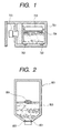
- Fig. 1 two (a pair of) electrodes 702 are arranged on the inner face of an ink tank 701 on the bottom side where non-conductive ink is filled, and then, a float 703 having electrodes 704 arranged to face the electrodes 702 is provided to float in ink in the ink tank 701.
- the two electrodes 702 are connected to the detecting section (not shown) that detects the conductive condition of both electrodes, respectively. Then, when the conductive condition of both electrodes is detected, the ink remainder error is issued to indicate that there in no more ink in the ink tank 701, and the operation of ink jet recording head 705 is suspended.
- the ink cartridge 805 for use of ink jet printer is disclosed, which is structured to form the lower part thereof in the funnel form toward the bottom face, and at the same time, two conductors 801 and 802 are arranged on the bottom face as shown in Fig. 2. Then, the metallic ball 804 having a smaller gravity than ink 803 is arranged in the interior thereof. With the structure thus arranged, the liquid surface of ink 803 is lowered as ink 803 is consumed. Along with this, the position of the metallic ball 804 that floats on the surface of ink 803 is gradually lowered.
- the pressure information in the ink tank, the changes of physical properties of ink, and the like are important parameters for the ink jet recording head to operate at all the time in a stable amount of ink dischargers.
- an ink tank which is capable of not only providing the detected information of the internal condition of ink tank on one-way for the outside, but also, capable of exchanging information bidirectionally, such as to provide the internal information in response to inquires from the outside.
- the structure is proposed so that ink tank is formed per color, and that only the ink tank having no more ink in it is made replaceable independently.
- the color ink tank of the kind it is necessary to install each ink tank on the designated position per color.
- to differentiate the ink tank configurations in a number of ink colors leads to the increased costs of ink tank. Therefore, it is desired to provide the ink tank that can deal with the improvement of installation aspect, while keeping each of ink tanks in the same configuration.
- the ink jet recording apparatus is provided with a plurality of nozzles (discharge ports) for discharging ink, and the ink which is supplied from the ink tank to the recording head is retained in each of the nozzles by means of the balance of capillary phenomenon and surface tension.
- ink is caused to leak from nozzles if the internal pressure of ink tank is higher than the atmospheric pressure.
- it is necessary to make the internal pressure negative in the ink tank.
- an ink tank is an airtightly closed container, the negative pressure in the ink tank becomes higher along with the consumption of ink in the ink tank. Then, with the negative pressure which should become too high, ink in the nozzles is drawn to the ink tank side to cause such drawback as inability to discharge ink when the recording head is driven to discharge ink from the nozzles.
- an ink absorbent of porous material, fibrous material, or the like is contained partially or totally in the interior thereof, and at the same time, the chamber in which the ink absorbent is contained is conditioned to be communicative with the air outside, thus enabling the ink absorbent to absorb and retain ink. In this manner, the interior of ink tank is conditioned to be in negative pressure.
- ink is retained by enabling ink absorbent to absorb it with the result that the efficiency of ink storage is lowered inevitably.
- the interior of ink tank is conditioned to be communicative with the air outside, the negative pressure becomes higher when the amount of ink retained in the ink absorbent becomes smaller, and there is still a possibility that the discharges of ink from the recording head is disabled depending on the relations with the external pressure exerted on the ink tank. Therefore, if it is possible to provide an additional function to an ink tank so as to adjust the pressure in the interior of the ink tank, any ink absorbent is no longer needed, and also, the efficiency of ink storage is enhanced. Here, it is desired to provide an ink tank having such function. Also, in order to adjust the pressure in the interior of ink tank, there is a need for knowing the condition of internal pressure of ink tank by all means directly or indirectly.
- the development of ink jet recording technologies is remarkable, and the printing accuracy thereof has become extremely high in recent years.
- the ink jet recording technologies can be utilized even for producing securities, official documents, or the like.
- the printer system used for producing those documents it is required to provide the security function so that the ink jet printer cannot be used by any one other than the owner or the authorized person by registration.
- the inventors hereof have given attention to the ball semiconductor manufactured by the Ball Semiconductor Inc., in which semiconductor integrated circuit is formed on the spherical surface of a silicon ball of approximately 1 mm diameter. Since this ball semiconductor is spherical, it is expected that the detection of surrounding environmental information and the bidirectional information exchange with the outside can be carried out efficiently in a better condition than the flat type semiconductor if the ball semiconductor is contained in the ink tank.
- the ball semiconductor manufactured by the Ball Semiconductor Inc., in which semiconductor integrated circuit is formed on the spherical surface of a silicon ball of approximately 1 mm diameter. Since this ball semiconductor is spherical, it is expected that the detection of surrounding environmental information and the bidirectional information exchange with the outside can be carried out efficiently in a better condition than the flat type semiconductor if the ball semiconductor is contained in the ink tank.
- the ball semiconductor device itself should be developed in order to provide such function as described above. Also, there some more problems to solve before the ball semiconductor device is effectively used for an ink tank.
- a novel device should be provided in order to form means for accumulating information on such a device as the ball semiconductor, and that the novel device should be capable of making itself very small at first, and then, capable of being driven with a small amount of power dissipation, while keeping information without being influenced by the fluctuation of energy supplied from the power-supply system, and if required, being able to rewrite information.
- Another problem is that the provision of an ink tank which is capable of performing the bidirectional exchange of information such as to receive inquiries from the outside and return internal information, not only by performing the one-way transmission of the detected internal information of ink tank to the outside.
- Still another problem is that the device that accumulates information should be driven by the application of low electric power, together with the provision of power supply system to actuate the device contained in the tank. If the power-supply source should be built in the ink tank to actuate the device, the tank inevitably becomes larger. Even when the power-supply source is provided outside the tank, it is still necessary to arrange means for connecting the power-supply source and the device. This inevitably increases the costs of tank manufacture. Thus, the tank cartridge should become expensive. Therefore, the device should be actuated from the outside by use of non-contact means.
- the device should float on the ink liquid surface in the ink tank or should be capable of residing in ink with a designated depth from the liquid surface. For example, it is desirable to position the device on the ink liquid surface in order to monitor the changing amount of negative pressure in time series along with the consumption of ink in the ink tank, but it is difficult to enable the device to float on ink, because it is formed by silicon having a specific gravity greater than water.
- the solid (three-dimensional) type semiconductor device of the present invention comprises energy converting means for converting energy from outside, and operating means operated by energy converted by the energy converting means.
- the method of the present invention for manufacturing a solid type semiconductor device comprises the steps of forming a protection film A on the entire surface of Si; forming opening on a part of the protection film A; removing only the upper part of the Si; forming a protection film B on the inner and outer surfaces of the work formed by the Si and protection film A; making the hollow portion in airtightly closed condition by use of conductive material; and forming conductor coil made by the conductive material.
- the method of the present invention for manufacturing a solid type semiconductor device comprises the steps of forming a protection film A on the entire surface of Si; forming opening on a part of the protection film A; removing only the upper part of the Si; forming a protection film B on the inner and outer surfaces of the work formed by the Si and protection film A; making the hollow portion in airtightly closed condition by use of conductive material and forming conductive film on the entire surface thereof; and patterning the conductive film to from conductor coil made by conductive material.
- the security system of a recording apparatus is provided with a recording head cartridge detachably mounted thereon, in which the recording head cartridge comprises a recognized data holding portion for holding as recognized data the personal information recognized by recognizing portion for recognizing personal information; a key code A holding portion for holding key code A; an encode converting portion for encoding the recognized data by the key code A; an encoded data holding portion for holding the encoded data by the encode data converting portion; an information input and output portion for receiving the key code A from the recording apparatus side, and for transmitting the recognized data and the encoded data to the recording apparatus; an energy converting portion for converting electromotive force supplied from the recording apparatus side in non-contact into electric power for actuating each of structural portions, and then, the recording apparatus comprises an energy supplying portion for supplying electromotive force to the energy converting portion in non-contact; a key code K setting portion for the owner of recording apparatus to set the key code K; a key code A holding portion and a key code B holding portion for holding key code A and
- the ink tank of the present invention is characterized in that at least one solid type semiconductor device arranged therefor which comprises energy converting means for converting energy from the outside; and operating means operated by energy converted by the energy converting means.
- the ink tank which contains ink to be supplied to a discharge head for discharging ink, and holds negative pressure in the interior thereof, comprises pressure adjustment means for adjusting negative pressure in the interior in accordance with negative pressure in the interior; and energy converting means for converting energy provide from the outside into energy of different kind from the energy for operating the pressure adjustment means.
- the method of the present invention for adjusting pressure which uses a solid type semiconductor device arranged for a container holding negative pressure in the interior thereof, and which is provided with pressure adjustment means for adjusting negative pressure inside the container in accordance with the internal pressure of the container, and energy converting means for converting energy provided from outside into different kind of energy from the energy in order to operate the pressure adjustment means, comprises the step of keeping pressure inside the container regularly by comparing pressure detected by the pressure detecting means for detecting pressure inside the container with the pressure inside the container.
- the memory element of the present invention comprises energy converting means for converting external energy supplied from the outside in non-contact into electric power, in which personal information is held by actuating the electric power.
- metalcenter means the intersection point of the line of action of weight at the time of being balanced, and the line of buoyance at the time of inclination.
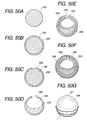
- solid type of the “solid type semiconductor device” is meant to include all the various three-dimensional shapes, such as a triangle, a sphere, a semi-sphere, a square column, a rotatively elliptical body, a mono-axially rotative body, among some others.
- the method for supplying external energy it should be good enough if only means for supplying electromotive force to the device as the external energy is arranged in the recovery position, returning position, or arranged for the carriage, head, or the like when this method is applied to an ink jet recording apparatus. Besides this, if only an apparatus having means for supplying electromotive force is used, it becomes possible to detect internal conditions of an ink tank without ink jet recording apparatus. For example, therefore, this method can be adopted for carrying out inspection or the like at a factory or a shop (for quality guarantee).
- the description will be made of the embodiments in accordance with the present invention. Then, the detailed description will be made of the embodiments particularly when the device is arranged for the interior of an ink tank.
- the device is not only used for the ink tank, but for other objects, and the same effect is obtainable.
- Fig. 3 is a block diagram which shows the inner structure of a solid type semiconductor device in accordance with a first embodiment of the present invention, and also, represents the communicative condition thereof with the outside.
- the solid type semiconductor device 11 shown in Fig. 3 comprises the energy converting means 14 which converts the electromotive force 12 supplied from the outside A to the device 11 in non-contact into electric power 13; information acquiring means 15 actuated by electric power obtained by energy converting means 14; discriminating means 16; information accumulating means 17; and information communicating means 18.
- This device is arranged in an ink tank.
- electromagnetic induction, heat, light, radiant rays. or the like is preferably usable.
- At least energy converting means 14 and information acquiring means 15 are formed on the surface or near the surface of the device.
- information accumulating means 17 should preferably be structured using FeRAM (Ferroelectric Random Access Memory) formed by ferroelectrics.
- Information acquiring means 15 is the one for acquiring information inside the ink tank, which is the environmental information surrounding the device 11.
- Discriminating means 16 compares the tank internal information obtained from information acquiring means 15 with information stored on information accumulating means 17 and determines whether or not the tank internal information thus obtained should be transmitted to the outside.
- Information accumulating means 17 accumulates various conditions which should be compared with acquiring tank internal information, as well as the tank internal information obtained from information acquiring means 15.
- Information communicating means 18 converts electric power into energy to be communicated as tank internal information in accordance with instructions from discriminating means 16, and displays the tank internal information and communicate it to the outside B.
- information acquiring means which is applicable to the solid type semiconductor device is exemplified for description.
- information acquiring means may be structured in such a manner that (1) SiO 2 film or SiN film is formed as ion sensitive film to provide a sensor for detecting pH in ink or (2) provide a pressure sensor of a diaphragm structure to detect pressure changes in the tank or (3) to provide a sensor for detecting the current position for the detection of ink remainders by incorporating photodiode capable of converting light into thermal energy for the production of pyroelectric effect or (4) to provide a sensor for detecting the presence or absence of ink depending on the amount of moisture in the tank by use of conductivity of material used the sensor, among some others.
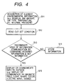
- Fig. 4 is a flowchart which illustrates the operation of device shown in Fig. 3.
- energy converting means 14 converts the electromotive force 12 into the electric power 13.
- information acquiring means 15, discriminating means 16, information accumulating means 17, and information communicating means 18 are actuated.
- Information acquiring means 15 thus actuated acquires information inside the ink tank, which is the environmental information that surrounds the device, such as ink remainders, the kind of ink, temperature, pH, and internal pressure (step S11 in Fig. 4). Then, discriminating means 16 reads out from information accumulating means 17 the conditions which are compared with the tank internal information thus obtained (step S12 in Fig. 4). Thus, the conditions thus read out are compared with the tank internal information thus acquired to determine whether or not information should be communicated (step S13 in Fig. 4).
- the discrimination made on the basis of the conditions predetermined for information accumulating means 17 are such as to determine that tanks should be replaced, because the ink remainders become less than the designated value (2 milliliters, for instance) or the Ph of ink, the internal pressure, or the like has changed greatly, for example.
- step S13 if it is determined by discriminating means 16 that there is no need for the current inner condition of ink tank to be communicated to the outside, the information of the current condition inside the ink tank is accumulated on information accumulating means 17 (step S14 in Fig. 4).
- this accumulated information may be compared with the next information acquired by information acquiring means 15.
- step S13 if discriminating means 16 determines that tank internal information should be communicated to the outside, the electric power which is obtained by means of energy conversion is converted by information communicating means 18 into energy for communicating the ink tank internal information to the outside.
- information communicating means 18 it is possible to use magnetic field, light, shape, color, electric wave, sound, or the like as energy for effectuating this communication.
- sounds are made to inform the outside B (ink jet recording apparatus, for instance) of the need for replacing tanks (step S15 in Fig. 4).
- the communicating end is not necessarily an ink jet recording apparatus, but it may be the eyesight or auditory sense of a human when light, shape, color, or sound is used in particular. Further, it may be possible to change communicating means such as using sound for communication regarding ink remainders, but using light for communication regarding pH of ink, or the like.
- the solid semiconductor device structured herein When the solid semiconductor device structured herein is used for an ink jet recording apparatus, it is possible to install means for supplying the electromotive force to this device as external energy on a recover position where recovery operation is performed; on a returning position where the carriage returns in the recording operation; on the carriage itself; or on the head itself or the like. Besides this arrangement, it may be possible to know the inner condition of ink tank without using an ink jet recording apparatus if only there is a device which is provided with means for supplying such electromotive force. Then, for example, it may be possible to use the device effectively for inspecting an ink tank, among some others, at a factory or at a shop, thus selling ink tank with a guarantee of quality.
- the device is provided with energy converting means.
- the device can be arranged for use in any location in an object, such as in ink as shown in Fig. 13 to Fig. 16 as described later. With the device being arranged in ink, it becomes possible to grasp the current condition of ink exactly in real time.
- electromotive force is supplied in non-contact mode, but it may be possible to adopt the mode in which electromotive force is supplied by being provisionally in contact with the outside, and subsequently, it becomes non-contact with the outside.
- the FeRAM formed by ferroelectrics when used as information accumulating means 17, it becomes capable of reading and writing data at high speed like a generally used DRAM (Dynamic Random Access Memory), and also, this means becomes non-volatile memory that can retain data even with the power-supply being cut off. Like this, the FeRAM makes higher access possible. Then, since the FeRAM is non-volatile it does not eliminate data even if the power-supply is instable, hence making the solid type semiconductor device effectively usable for an ink tank. With the FeRAM that stores information to be accumulated, it becomes possible to perform information processing exactly, as well as to perform bidirectional signal communications with the external equipment at a low voltage to drive this means.
- DRAM Dynamic Random Access Memory
- the device can be formed smaller, which can be driven at low voltage.
- the FeRAM makes high speed access possible, while it is non-volatile so as not to eliminate data even with a power-supply being instable, and, further, miniaturization possible at low power dissipation.
- the FeRAM is formed as extremely effective information accumulating means for the solid type semiconductor device. It is particularly effective for an ink tank to use the solid type semiconductor device with these advantages in view, which will be described later.
- Fig. 5 is a block diagram which shows the inner structure of a solid type semiconductor device in accordance with a second embodiment of the present invention, and also, represents the communicative condition thereof with the outside.
- the solid type semiconductor device 21 of the present embodiment shown in Fig. 5 comprises energy converting means 24 for converting into electric power 23 the electromotive force 22 which is supplied in non-contact from the outside A toward the device 21; information acquiring means 25 actuated by the electric power which is obtained by energy converting means 24; discriminating means 26; information accumulating means 27; information communicating means 28; and reception means 29.
- These means are arranged in an ink tank. What differs from the first embodiment is that there is provided a function to receive signals.
- electromagnetic induction, heat, light, radiation rays, or the like is applicable as the electromotive force which is required to operate the device.
- Information acquiring means 25 acquires the information inside the ink tank, which is the environmental information surrounding the device 21.
- Reception means 29 receives input signals 20 from the outside A or outside B.
- Discriminating means 26 enables information acquiring means 25 to acquire the tank internal information in accordance with the input signals from reception means 29, and compares the tank internal information thus acquired with the information stored on information accumulating means 27 to determine whether or not the acquired tank internal information satisfies the designated conditions.
- Information accumulating means 27 accumulates various conditions to be compared with the tank internal information to be acquired, as well as the tank internal information acquired from information acquiring means 25.
- Information communicating means 28 converts electric power by the instruction from discriminating means 26 into energy for communicating to the tank internal information, and then, displays the result of discrimination provided by discriminating means 26 on the outside A, outside B, or outside C and communicates therewith accordingly.
- Fig. 6 is a flowchart which illustrates the operation of device shown in Fig. 5.
- the electromotive force 22 is supplied from the outside A toward the device 21, and then, energy converting means 24 converts the electromotive force 22 to electric power 23.
- information acquiring means 25, discriminating means 26, information accumulating means 27, information communicating means 28, and reception means 29 are actuated.
- the outside A or outside B transmits to the device 21 the signal 30 which is used for inquiring the information inside the ink tank.
- This input signal 30 is, for example, the signal whereby to inquire whether or not ink still remains in the ink tank, which is received by reception means 29 (step S21 in Fig. 6).
- discriminating means 26 enables information acquiring means 25 to acquire the information inside the ink tank, such as the amount of ink remainders, the kind of ink, temperature, and pH (step S22 in Fig. 6), and also, to read out the conditions from information accumulating means 27 to which the acquired tank internal information is referenced (step S23 in Fig. 6), thus determining whether or not the acquired information satisfies the set conditions (step S24 in Fig. 6).
- step S24 If it is found in the step S24 that the acquired information does not satisfy the set conditions, the message of being unsatisfied is communicated to the outside A, outside B or outside C. If it is found that the acquired information satisfies the set conditions, the message is communicated accordingly (step S25 and step S26). At this juncture, it may be possible to communicate with the outside regarding the acquired information together with the result of discrimination. This communication is carried out by the information communicating means 28 which converts the electric power obtained by energy conversion into energy for communicating the information inside the ink tank to the outside.
- the communication mode may be changeable in accordance with the result of discrimination, and also, in accordance with the contents of question to be answered (for example, whether or not the ink remainders are less than a designated amount (2 milliliters, for instance) or whether or not the pH of ink has changed or the like).
- electromotive force for the device 21 together with input signal 30 from the outside A or outside B.
- the electromotive force may be used separately as signal for inquiring of the ink remainders if it is electromagnetic induction, and as signal for inquiring of the pH condition of ink if it is light.
- the function to receive signals from the outside Therefore, in addition to the effects obtainable from the first embodiment, it becomes possible for the present embodiment to answer various signalized questions from the outside, hence making it possible to perform communications between the device and outside bidirectionally.
- the fundamental structure of the present embodiment is the solid type semiconductor device having no information acquiring means, but capable of outputting the information stored in advance on the device to the outside in response to the input signals from the outside.
- Fig. 7 is a block diagram which shows the inner structure of a solid type semiconductor device in accordance with a third embodiment of the present invention, and also, represents the communicative condition thereof with the outside.
- the solid type semiconductor device 31 of the present embodiment shown in Fig. 7 comprises energy converting means 34 for converting into electric power 33 the electromotive force 32 which is supplied in non-contact from the outside A toward the device 31; buoyance generating means 35 for generating buoyance by use of the electric power which is obtained by energy converting means 34.
- These means are arranged in an ink tank.
- energy converting means 34 converts the electromotive force 32 into the electric power 33.
- buoyance generating means 35 generates buoyance so as to enable the device 31 to float on the ink liquid surface. This buoyance is not necessarily arranged to reside on the ink liquid surface, but enable the device to be positioned below the ink liquid surface by a specific distance under any circumstances so as to prevent discharge from being effectuated in a state where ink is not available.
- Fig. 8A and Fig. 8B illustrate the positions of device 31 residing in ink in the ink tank along with the changes of ink consumption.
- ink is retained in the negative pressure generating member 37 in an amount equivalent to the ink which has been consumed along with ink being led out from the negative pressure generating member 37 through the ink supply port 36.
- the solid type semiconductor device 31 in ink 38 moves along with the lowered position of ink liquid surface H due to ink consumption while it still resides below the ink liquid surface H by a specific distance (Fig. 8B).
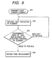
- Fig. 9 is a flowchart to confirm the position of device 31, and determine whether or not it is necessary to replace tanks.
- light is emitted from the outside A or outside B (an ink jet recording apparatus, for instance) toward the device 31. Then, the light is received by the outside A, outside B (the ink jet recording apparatus, for instance), or outside C, thus detecting the position of device 31.
- the ink jet recording apparatus is then allowed to determine whether or not it is necessary to replace tanks or the like by the detected position of device. If it is found necessary to replace tanks, notification is made accordingly by use of sound or light.
- light emitting means and photosensitive means are arranged to face each other to confirm the position of device when no light is allowed to pass the device or to confirm it when photosensitive means senses the reflection of light emitted from liquid emitting means. Further, as described later, it may be possible to arrange the structure so that the solid type semiconductor device 31 itself becomes light emitting means, and emits light toward photosensitive means provided outside the tank.
- the device it becomes possible to use the device irrespective of the environment surrounding the device, because the device can be positioned always at a desired location by converting the electromotive force from the outside using energy converting means even when the buoyance or the like required for the device may change due to the difference in gravity of liquid or other environmental conditions where the device is used.
- present embodiment may be combined with the first and second embodiments described above.
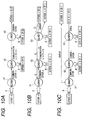
- Figs. 10A to 10C are conceptual views which illustrate the method for using the solid type semiconductor device in accordance with a fourth embodiment of the present invention.
- the present embodiment is structured by adding to the solid type semiconductor device of the first or second embodiment a function to communicate information to other devices, and a plurality of such devices are arranged in an object.
- a plurality of solid type semiconductor devices of the first embodiment are arranged in the object.
- electromotive force E is supplied from the outside A or outside B to each of the devices, each of them acquires the environmental information surrounding each of them, respectively.
- the acquired information a of the device 41 is communicated to the device 42, and the acquired information a and b of the device 41 and device 42 are communicated to the next device one after another.
- the last device 43 communicates all the acquired information to the outside A or outside B.
- a plurality of solid type semiconductor devices of the second embodiment are arranged in an object, and electromotive force E is supplied from the outside A or outside B to each of the devices.
- electromotive force E is supplied from the outside A or outside B to each of the devices.
- the device 51 or device 52 which corresponds to the contents of such question, acquires information corresponding to the question and answers it.
- the answer from the device 51 or device 52 to such question is communicated to other devices one after another, and the answer is made from the desired device 53 to the outside A, outside B or outside C.
- a plurality of solid type semiconductor devices of the second embodiment are arranged in an object, and electromotive force E is supplied from the outside A or outside B to each of the devices. Then, when a certain signal is inputted from the outside A or outside B to the device 63, for example, such signal is communicated to the device 62 and device 61 one after another, and displayed from the device 63 on the outside A, outside B or outside C.
- the solid type semiconductor device of the third embodiment which is provided with buoyance generating means, may be used as one of plural solid type semiconductor devices.
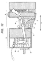
- Fig. 11 shows the structural example in which solid type semiconductor devices are arranged by appropriately combining those of the first, the second or the third embodiment in an ink tank and a recording head, respectively.
- a reference mark W designates the directions of printing scans
- E electromotive force.
- the solid type semiconductor device 71 which is formed by adding to the first embodiment the device of third embodiment having buoyant generating means, and also, having information communicating function to the other device 79, is arranged in a desired position in ink 73 in the ink tank 72.
- the solid type semiconductor device 79 is arranged, which is formed by adding ID function (identifying function) to the solid type semiconductor device of second embodiment.
- the power supply to the device 79 may be made by the contact between the electrode portion arranged on the surface of the device and the contacting portion on the surface of electric base board arranged to drive the recording head 78.
- the device 71 in ink acquires ink remainder information, for example, and the device 79 on the recording head side communicates to the device 71 the ID information which is needed for determining the replacement of ink tanks. Then, the device 71 compares the acquired ink remainder information with the ID information. If there is agreement between them, it communicates with the device 79 to instruct the outside for the tank replacement. When receiving such communication, the device 79 transmits signals to the outside for the tank replacement or outputs sound or light to appeal the eyesight or auditory sense of human being accordingly.
- Figs. 10A to 10C and Fig. 11 are structured to supply electromotive force to each of solid type semiconductors, but the arrangement is not necessarily limited thereto. It may be possible to arrange structure so that the electromotive force supplied to a certain device is transmitted to the other devices one after another together with required information. For example, as shown in Fig.
- the solid type semiconductor device 81 which is formed by adding to the first embodiment the buoyance generating means of third embodiment, function to communicate information to other devices, as well as electromotive force supplying function
- the solid type semiconductor device 82 which is formed by adding to the second embodiment the buoyance generating means of third embodiment, function to communicate information to other devices, as well as electromotive force supplying function
- the solid type semiconductor device 83 of second embodiment which is provided with the ID function (identifying function).
- the electric power supply to the device 83 may be made by contacting the electrode portion on the surface of the device with the contacting portion on the electric base board arranged to drive the recording head 78.
- a reference mark E designates electromotive force, and W, the directions of printing scans.
- the device 81 which resides in ink acquires ink remainder information, for example, and compares this information with the regulated inner conditions, and if communication with the other devices is found necessary, the ink remainder information thus acquired is communicated to the device 82 together with electromotive force to operate the device 82.
- the device 82 which has received the supply of electromotive force receives the ink remainder information communicated from the device 81, and at the same time, acquires information regarding pH of ink, for example, and then, transmits electromotive force to the device 83 on the recording head side to operate the device 83.
- the device 83 on the recording head side which receives electromotive force thus supplied, communicates ID information to the device 82 for determining the ink remainders which necessitates the replacement of tanks or determining the current pH of ink. Then, the device 82 compares the acquired ink remainder information and pH information with the ID information thus communicated, and if in agreement, communicate with the device 83 to instruct the outside for replacing tanks. Receiving this instruction, the device 83 transmits signals to the outside for replacing tanks or outputs sound, light, or the like to appeal the eyesight or auditory sense of human being accordingly. In this way, conceivably, there is a method for supplying electromotive force from a certain device to other devices together with required information.
- the recording head 78 it is possible for the recording head 78 to adopt the discharge mode known in the field of ink jet recording, in which ink is bubbled in liquid flow path by the application of heat generated by heater or the like, such as electrothermal converting device, thus discharging ink from each of fine openings communicated with each of the liquid flow path, respectively, or to adopt the structure in which ink is discharged by driving piezoelectric device.
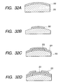
- Fig. 13 to Fig. 16 are views which illustrate the structure of an ink tank to which the solid type semiconductor device of the above embodiments is applicable.
- the ink tank 501 shown in Fig. 13 has a flexible ink bug 502 containing ink therein arranged in a housing 503, and the bug opening 502a is closed by means of a rubber plug 504 fixed to the housing 503. Then, when the hollow needle 505 which is used for leading out ink is pierced through the rubber plug 504, ink is supplied to an ink jet head (not shown).
- the solid type semiconductor device 506 of the present invention can be arranged in the ink bug 502 of such ink tank 501 as this.
- an ink tank 511 shown in Fig. 14 is such that the ink jet head 515 that records by discharging ink to a recording sheet S is installed on the ink supply port 514 of the housing 512 containing ink 513. It is possible to arrange the solid type semiconductor device 516 of the present invention in ink 513 in the tank 511.
- an ink tank 521 shown in Fig. 15 is the same tank as the one shown in Figs. 8A and 8B, Fig. 11, and Fig. 12, which comprises a completely closed first chamber for containing ink 522; a second chamber containing a negative pressure generating member 523 in a state of being communicated with the air outside; and the communicative passage 524 to enable the first chamber and the second chamber to be communicated on the lowest portion of the tank.
- ink 522 in the first chamber is led out to the second chamber in place of the air outside that enters the first chamber from the second chamber side.
- the solid type semiconductors 525 and 526 are arranged each in the first chamber and the second chamber, respectively. It is advisable to let them communicate with each other regarding ink in each of the separated chambers.
- an ink tank 531 shown in Fig. 16 is such that a porous member 532 retaining ink is housed, and then, an ink jet head 533 is installed thereon to use ink thus retained for recording.
- the solid type semiconductors 534 and 535 are arranged each in the ink tank side and the ink jet head side, respectively. It is advisable to let them communicate with each other regarding ink in each of the separated structures.
- Fig. 17 is a view which schematically shows the structure of an ink jet recording apparatus having mounted thereon the ink tank which is provided with the solid type semiconductor device of the present invention.
- the head cartridge 601 which mounted on the ink jet recording apparatus 600 shown in Fig. 17 comprises a liquid discharge head to discharge ink for recording prints, and an ink tank as shown in Fig. 13 to Fig. 16 in order to retain liquid to be supplied to the liquid discharge head.
- means 622 for supplying electromotive force serving as external energy to the solid type semiconductor device (devices) arranged in the ink tank, and means (not shown) for communicating information to and from such device bidirectionally.
- the head cartridge 601 is mounted on the carriage 607 which engages with the spiral groove 606 of a lead screw 605 rotative through the driving power transmission gears 603 and 604 which are interlocked with the regular and reverse rotations of a driving motor 602.
- the head cartridge 601 reciprocates by driving of the driving motor 602 together with the carriage 607 along the guide 608 in the directions indicated by arrows a and b.
- the ink jet recording apparatus 600 is provided with means for carrying recording medium (not shown) for carrying a printing sheet P serving as the recording medium that receives liquid, such as ink, discharged from the cartridge 601.
- the pressure plate 610 for the printing sheet P carried on a platen 609 by means for carrying recording medium is arranged to press the printing sheet P to the platen 609 over the traveling directions of the carriage 607.
- photocouplers 611 and 612 are arranged.
- the photocouplers 611 and 612 constitutes the home position detecting means which recognizes the presence of the lever 607a of carriage 607 in the region formed by the photocouplers 611 and 612 in order to switch the rotational directions of driving motor 602.
- a supporting member 613 is arranged to support the cap member 614 that covers the front end of discharge ports of head cartridge 601.
- ink suction means 615 is arranged to suck ink residing inside the cap member 614 due to idle discharges from the head cartridge 601 or the like. With this ink suction means 615, the suction recovery is carried out for the head cartridge 601 through the opening of cap member 614.
- a main body supporting member 619 is provided.
- a movable member 618 is movably supported in the front and backward directions, that is, in the direction at right angles to the traveling direction of the carriage 607.
- a cleaning blade 617 is installed on the movable member 618.
- the mode of cleaning blade 617 is not necessarily limited thereto. Any known modes of cleaning blade may be usable.
- the lever 620 is arranged for initiating suction when suction recovery operation is carried out by use of ink suction means 615.
- an ink jet recording controller is arranged to transmit signals to the heat generating elements which are provided for the head cartridge 601, and also, execute the driving controls of each of the mechanisms described earlier. This controller is not shown in Fig. 17.
- the ink jet recording apparatus 600 thus structured enables the head cartridge 601 to reciprocate over the entire width of a printing sheet P.
- the printing sheet P is carried on the platen 609 by use of the aforesaid means for carrying recording medium.
- driving signals are supplied from means for supplying driving signals (not shown) to the head cartridge 601 at the time of this movement, ink (recording liquid) is discharged from the liquid discharge head unit to the recording medium for recording in accordance with such signals.
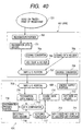
- Fig. 18 is a block diagram which shows the inner structure of the solid type semiconductor device in accordance with a fifth embodiment of the present invention, and the communication thereof with the outside.
- the solid type semiconductor device 91 shown in Fig. 18 comprises energy converting means 94 for converting into electric power 93 the electromotive force 92 which is external energy supplied in non-contact from the outside A toward the device 91; and light emitting means 95 for emitting light by use of the electric power which is obtained by energy converting mean 94.
- the device is arranged ink in an ink tank.
- Light emitting means 95 is formed by photodiode or the like.
- electromagnetic induction, heat, light, radiation rays, or the like is usable as the electromotive force which is supplied to operate the device. Also, it is desirable to form energy converting means 94 and light emitting means 95 on the surface of device or near thereto.
- energy converting means 94 converts electromotive force 92 into electric power 93. Then, using the electric power 93 light emitting means 95 emits light 96. The intensity of light 96 thus emitted from light emitting means 95 is detected by the outside B.
- Fig. 19 is a structural view which schematically shows the ink tank that uses the solid type semiconductor device 91 illustrated in accordance with the fifth embodiment.
- the solid type semiconductor device 91 shown in Fig. 19 floats near the liquid surface of raw ink 522 in the ink tank 521, and electromotive force is induced by electromagnetic induction provided by external resonance circuit (not shown) outside the ink tank 521. Then, the photodiode which is arranged near the surface of solid type semiconductor device 91 is driven to emit light. The light transmits through ink 522 to be received by the external photosensor 97 of the ink tank 521.
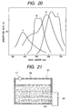
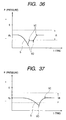
- Fig. 20 is a view which shows the extinction wavelength (absorbance spectrum) of typical ink (yellow (Y), magenta (M), cyan (C), and black (B)).
- Y yellow
- M magenta
- C cyan
- B black
- the peak of extinction ratio of each color ink, yellow, magenta, cyan, and black is dispersed in the wavelength band of 300 to 700 nm.
- the light the wavelength of which is included in a range of 300 to 700 nm is emitted from the solid type semiconductor device, and then, such light is received by the light sensor 97 (see Fig. 19) outside the ink tank after being transmitted through ink for detection of the most absorbed wavelength. In this manner, it is possible to discriminate the ink color through which the light has transmitted among the aforesaid colors of ink.
- the extinction ratio of each ink of yellow, magenta, cyan, and black colors is distinctly different at the wavelength of 500 nm.
- the extinction ratio of each ink color at the wavelength of 500 nm is: magenta approximately 80%, black approximately 50%, yellow approximately 20%, and cyan approximately 5%. Therefore, with the detection of intensity rate (transmissivity) of transmitted light through ink against the intensity of light emitted from the solid type semiconductor device with respect to light having wavelength of 500 nm, it is possible to discriminate the color of ink that allows the light to transmit through from ink of those colors described above.
- the ink jet recording apparatus which is structured to install each of plural ink tanks on each designated position in accordance with the kind of ink contained in each of such ink tanks, it is advisable to arrange means for issuing warning to the user by use of the light sensor 97 that receives light transmitted through ink in the ink tank when it is detected that the ink tank is not installed adequately as designated.
- warning means in this case, light emitting means such as lamp or sounding means such as buzzer may be useable. The user notices by the warning thus issued by such means that the ink tank is installed on an inadequate position so that he can install it again on the designated position exactly.
- an ink jet recording apparatus of the kind may arrange control means for controlling the recording head depending on the kind of ink to be supplied to such recording head from the ink tank installed thereon when it is detected by the light sensor that receives light transmitted through ink in the ink tank that the ink tank is installed on an inadequate position.
- control means for controlling the recording head depending on the kind of ink to be supplied to such recording head from the ink tank installed thereon when it is detected by the light sensor that receives light transmitted through ink in the ink tank that the ink tank is installed on an inadequate position.
- energy converting means for converting external energy into different kind of energy
- light emitting means for emitting light by use of energy thus converted by energy converting means. Therefore, it becomes possible to discriminate the kinds of ink by detecting the intensity of wavelength of transmitted light after light emitted from the solid type semiconductor device is allowed to transmit ink.
- the solid type semiconductor device described in accordance with the fifth embodiment, for which light emitting means is provided, may be usable as given below in addition to the utilization thereof in the ink tank for the discrimination of the kind of ink therein.
- the solid type semiconductor device provided with light emitting means is buried on the side face of a tube in which liquid flows so that the device is exposed in the tube, and then, on the opposite face thereof, a photosensitive device (this device may also be formed by the solid type semiconductor itself) is arranged.
- a photosensitive device this device may also be formed by the solid type semiconductor itself
- the device is preferably usable when data should be obtained by simulating the behavior of a structure or the like.
- solid type semiconductors each provided with light emitting means of a designated wavelength are appropriately arranged for the designated locations of a member required to perform a specific operation, and then, the structure is driven to operate for obtaining data by detecting the behavior of the devices.
- the result is obtainable by utilizing solid type semiconductor devices each capable of executing assigned functions in non-contact with the outside. More specifically, it is possible to detect the behavior of driving elements that operate for discharge the ink which has been distributed in the interior of an ink jet head.
- the devices each provided with light emitting means having wavelength of 300 nm, 400 nm, 500 nm, and 600 nm, respectively, are appropriately arranged for the driving elements, and then, by detecting light from the discharge port side, it becomes possible to measure the movement of each element for acquiring the behavioral information of each driving element.
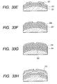
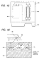
- Fig. 21 is a cross-sectional view which shows the ink tank schematically, to which the solid type semiconductor device in accordance with a sixth embodiment of the present invention is applicable.
- Fig. 22 is a structural block diagram which shows the inner structure of the solid type semiconductor device represented in Fig. 21, and the communicative condition thereof with the outside.
- the ink tank 101 comprises an ink containing chamber 102 that contains ink, and the ink supply port 103 through which ink in the ink containing chamber 102 is supplied to an ink recording head 104.
- the recording head 104 is connected detachably to the ink tank 101 or connected fixedly to the ink supply port 103. Recording is made on a recording medium by discharging from a plurality of discharge ports (not shown) the ink which is supplied from the ink tank 101 in accordance with recording signals.
- ink supplied from the ink tank 101 is retained in each of the discharge ports by the balance between capillary phenomenon and surface tension.
- the interior of ink containing chamber 102 is kept in negative pressure.
- the solid type semiconductor device (hereinafter referred to simply as “device”) 111 is fixed in the state where a part thereof is exposed outside the ink tank 101, while another part is exposed in the interior of ink containing chamber 102.
- the fixing position of the device 111 is not necessarily limited, but at least the portion which is exposed in the ink containing chamber 102 is positioned so as not to be in contact with ink when the ink tank 101 is in use or preferably, on the upper wall portion of ink tank 101 when it is in use.
- the ink tank 101 is a container the interior of which is essentially closed, and in order to prevent ink leakage from the discharge ports of recording head 104 when recording is not in operation, the interior of ink containing chamber 102 is kept at a designated negative pressure.
- the ink tank 101 is a container the interior of which is-essentially closed, the internal pressure of ink tank 101 is reduced along with the consumption of ink in the ink containing chamber 102. In other words, the negative pressure becomes higher. If the negative pressure in the ink tank 101 becomes too high, ink is not easily discharged if even it is intended to discharge ink from the recording head 104, and the event is encountered in some cases that ink cannot be discharged ultimately.
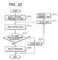
- the device 111 of the present embodiment is provided with the function to detect the inner pressure of ink tank 101, and then, to communicate the inner and outer side of ink tank 101 in accordance with the result of such detection, thus suppressing the negative pressure in ink tank 101 to rise.
- the device 111 comprises energy converting means 114 for converting into electric power 113 the electromotive force 112 which is supplied in non-contact from the outside A of ink tank 101 toward the device 111; pressure detecting means 115 actuated electric power 113 converted by energy contenting means 114; discriminating means 116; information accumulating means 117; and pressure adjustment means 118.
- electromagnetic induction, heat, light, radiation rays, or the like is usable.
- energy converting means 114 should preferably formed on the surface or near the surface of the device 111. In this respect, it is one of preferable structures that information accumulating means 117 is formed by FeRAM as described earlier.
- Pressure detecting means 115 detects the pressure inside the ink tank, which is the environmental information surrounding the device 111, and outputs it to discriminating means 116.
- the pressure sensor can be cited, which has diaphragm on the surface of the device 111, for example, and detects pressure by the displacement of diaphragm based on the pressure changes.
- Discriminating means 116 compares the tank internal pressure information thus detected by pressure detecting means 115 with the information stored on information accumulating means 117, and determines whether or not the detected information of tank internal pressure to pressure adjustment means 118.
- Information accumulating means 117 accumulates the condition of internal pressure which is the upper limit of negative pressure set for discharging ink from the recording head 104 installed on the ink tank 101, and also, the tank internal information itself detected by pressure detecting means 115.
- Pressure adjustment means 118 is driven by electric power given by energy converting means 114 and adjusts the internal pressure of ink tank 101 in accordance with the instruction from discriminating means 116.
- pressure adjustment means 118 a valve mechanism can be used, for example, so as to enable the interior of ink tank 101 to be communicated with the outside.
- the internal pressure of ink tank 101 is adjusted in accordance with the difference between the result of detection obtained by pressure detecting means 115 and the value of internal pressure of ink tank accumulated on information accumulating means 117. Then, the opening time of valve mechanism is controlled depending on such difference. In this manner, the internal pressure of ink tank 101 is made adequate.
- Fig. 23 is a flowchart which illustrates the operation of device represented in Fig. 22.
- energy converting means 114 converts the electromotive force 112 into electric power 113.
- pressure detecting means 115, discriminating means 116, information accumulating means 117, and pressure adjustment means 118 are actuated.
- the actuated pressure detecting means 115 detects the internal pressure of ink tank 101 (step S111 in Fig. 23). Then, discriminating means 116 reads out accumulated information from information accumulating means 117 (S112 in Fig. 23), and compares the condition thus read out with the detected information of tank internal pressure, hence determining whether or not adjustment is needed for the internal pressure of ink tank 101 (step S113 in Fig. 23).
- the ink tank 101 is set at an initial pressure by use of a dedicated inspection apparatus at the time of shipment from the factory after ink has been filled (step S116 in Fig. 23), and such information is written on ROM in the device 111 as initial information (step S117 in Fig. 23) as to the portion (indicated as an adequate range (R) in Fig. 36).
- a reference mark S designates the suspension of printing, and VO and VC, opening and closing of valve, respectively.
- step S113 if the detected internal pressure of ink tank 101 is within the range of internal pressure of ink tank 101 accumulated on information accumulating means 117, and then, discriminating means 116 determines that no adjustment is needed for the internal pressure of ink tank 101, pressure adjustment means 118 is not driven, and the current internal information of ink tank 101 is accumulated on information accumulated means 117 (step S114 in Fig. 23).
- Fig. 36 shows the example of accumulated internal information.
- step S113 if the detected negative pressure of ink tank 101 is lower than the value of upper limit set to the internal pressure of ink tank 101, which is accumulated on information accumulating means 117, and discriminating means 116 determines that the internal pressure of ink tank 101 should be adjusted, pressure adjustment means 118 is driven by the electric power 113 converted by energy converting means 115.
- pressure adjustment means 118 is a valve mechanism, the internal pressure of ink tank 101 is adjusted as described above (step S115 in Fig. 23).
- the preferable position where means for supply electromotive force as the external energy is the recording head, carriage, recovery position of recording head, or carriage return position, among some others, for the ink jet recording apparatus of serial type, for example.
- the internal pressure of ink tank may be adjusted without mounting the ink tank on the ink jet recording apparatus actually at a factory or a shop, for example.
- the device 111 provided for the ink tank 101, it becomes possible to detect the internal pressure of ink tank 101 and adjust it to a designated pressure if only electromotive force 112 is given to the device 111.
- the interior of ink tank 101 can be kept in a preferably negative condition suitable for discharging ink from recording head 104 irrespective of the amount of ink remainders in ink tank 101, hence making it possible to supply ink to the recording head 104 stably.
- the device 111 since the device 111 is provided with energy converting means 115, it is no longer necessary to provide any direct electrical wiring with the outside, and the device 111 can be used even in any location that makes electrical wiring difficult for direct connection with the outside. Further, with the device 111 having energy converting means 115 provide therefor, there is no need for providing the device 111 with any means for accumulating electromotive force (power-supply source for this example) for operating the device 111. Therefore, the device 111 can be made smaller, and the device 111 can be made usable in any locations in an object. In other words, the device 111 can be set at the optimal location in ink tank 101.
- electromotive force is supplied to the device 111 in the form of non-contact, but it may be possible to adopt a mode in which electromotive force is supplied by being in contact with the outside provisionally, and after that, it is made non-contact with the outside.
- Fig. 24 is a structural block diagram which shows the internal structure of the solid type semiconductor device in accordance with a seventh embodiment of the present invention, and the communicative condition thereof with the outside.
- the solid type semiconductor device shown in Fig. 24 (hereinafter referred to simply as the "device") 121 is fixed to an ink tank (not shown) in the same manner as the device 111 shown in Fig. 21, and comprises energy converting means 124 for converting into electric power 123 the electromotive force 122 which is supplied from the outside A of ink tank in non-contact toward the device 121; pressure detecting means 125, discriminating means 126, information accumulating means 127, pressure adjustment means 128, and reception means 129 actuated by the electric power thus converted by energy converting means 124.
- the present embodiment differs from the sixth embodiment in that it has the function to receive signals, that is, it has reception means 129.
- reception means 129 For the electromotive force 122 to be supplied to actuate the device 121, electromagnetic induction, heat, light, radiated rays or the like is usable. Also, at least energy converting means 124 and reception means 129 should preferably be formed on the surface of the device 121 or near the surface thereof.
- Pressure detecting means 125 detects the internal pressure of ink tank, which is the environmental information surrounding the device 121, and output it to the discriminating means 126.
- Reception means 129 receives input signals 130 from the outside A which is the supply source of electromotive force 122 or for the outside B which is different from the outside A.
- Discriminating means 126 enables pressure detecting means 125 to detect the internal pressure of ink tank in accordance with input signals from reception means 129, and compares the internal information of ink tank thus detected with information stored on information accumulating means 127, thus determining whether or not the detected information of internal pressure of ink tank satisfies the condition on which ink is discharged from the recording head (not shown) installed on the ink tank.
- Information accumulating means 127 accumulates such condition and ink information itself obtained from pressure detecting means 125.
- Pressure adjustment means 128 is driven by the electric power which is provided from energy converting means 124 to adjust the internal pressure of ink tank in accordance with the instruction from discriminating means 126.
- pressure detecting means 125 and pressure adjustment means 128, it is possible to use the same ones described in conjunction with the sixth embodiment.
- Fig. 25 is a flowchart which illustrates the operation of device shown in Fig. 24.
- energy converting means 124 converts electromotive force 122 into electric power 123 when the electromotive force 122 is given from the outside A toward the device 121, thus actuating pressure detecting means 125, discriminating means 126, information accumulating means 127, pressure adjustment means 128, and reception means 129.
- input signal 130 transmitted from the outside A or outside B to the device 121 is received by reception means 129 (step S121 in Fig. 25).
- This input signal 130 is to inquire the device 121 of the internal pressure of ink tank.
- the input signal 130 may be provided for the device 121 together with electromotive force 122.
- discriminating means 126 When the input signal 130 is received, discriminating means 126 enables pressure detecting means 125 to detect the internal pressure of ink tank (step S122 in Fig. 25), and reads out accumulated information for information accumulating means 127 (step S123 in Fig. 25), thus determining whether or not the detected internal pressure satisfies the aforesaid condition (step S124 in Fig. 25).
- the initial pressure is set for the ink tank by use of a dedicated inspection apparatus at the time of shipment from the factory after ink has been filled (step S126 in Fig. 25), and the information thereof is written as the portion (indicated as an adequate range (R) in Fig. 37) on the ROM of device 121 as initial information (step S127 in Fig. 25).
- step S124 if it is found that the detected internal pressure does not satisfy condition, pressure adjustment means 128 is driven to adjust the internal pressure of ink tank (step S125 in Fig. 25).
- step S125 if the detected internal pressure satisfies condition, the information of current internal pressure of ink tank is accumulated on information accumulating means 127 (step S128 in Fig. 25).
- Fig. 37 shows the example of accumulated information of internal pressure.
- reference marks VO and VC designate the opening and closing of valve, and S, the suspension of printing.
- Fig. 26 is a view which shows the one structural example of pressure adjustment means provided for the solid type semiconductor of the present invention, and illustrates the case where it is formed on the spherical silicon used for the aforesaid ball semiconductor.
- Figs. 27A to 27G are views which illustrate the manufacturing process of pressure adjustment means shown in Fig. 26.
- Fig. 26 and Figs. 27A to 27G are sectional views taken at the center of the spherical silicon.
- each of base electrodes 201 is formed respectively at two locations of spherical silicon 200, which face each other. Also, surrounding the spherical silicon 200, SiN film 206 is formed. The SiN film 206 is formed to be movable portions 210 and 211, which are supported in a cantilever fashion having a gap with the surface of the spherical silicon 200, respectively, on the areas where each of the base electrodes 201 faces each other. Each of the movable members 210 and 211 is provided with valve electrode 205 facing the base electrode 201, respectively. Also, the SiN film 206 has a gap locally with the spherical silicon 200 in each area from one base electrode 201 to the other electrode 201, respectively. Each of these portions becomes the passage 212 that makes it possible to distribute the air between one movable member 210 side and the other movable member 211 side.
- PSG (phospho silicate glass) film 202 shown in Fig. 27B is formed on the entire surface of spherical silicon 201 shown in Fig. 27A.
- each of base electrodes 201 is formed in advance on the spherical silicon 201 at each of the two locations which are symmetrical to the center thereof.
- the PSG film 202 is patterned by use of photolithographic process with the portions becoming passage left intact.
- Fig. 27D using metallic CVD method Cu film 204 is formed to cover the base electrodes 201 and PSG film 202.
- the Cu film 204 is removed with the base electrodes 201 and portions around them being left intact.
- valve electrodes 205 are formed on the portions of Cu film 204 which become movable portions to be described later.
- SiN film 206 is formed using PECVD method to cover the PSG film 202, the Cu film 204 and valve electrodes 205.
- the SiN film 206 is patterned to be in the form of movable members.
- Fig. 28 is a plan view which schematically shows the device at this stage. With the SiN film 206 patterning, radial slits 206a are formed on the Cu film 204 portion on SiN film 206 as shown in Fig. 28. Then, the Cu film 204 and PSG film 202 are removed by dissolution using adequate solvent. In this manner, as shown in Fig.
- an solid type semiconductor device is obtained, which is structured with the movable portions 210 and 211 on the two locations, each on the upper and lower portions, respectively, so as to function as valves supported with a gap to the spherical silicon 200, and then, a space between the upper movable member 210 and spherical silicon 200, and a space between the lower movable member 211 and spherical silicon 200 are connected with each other by the passage 212.
- one movable member 210 is positioned outside the ink tank, and the other movable member 211 is positioned inside the ink tank for installation.
- Fig. 29 is a view which shows the equivalent circuit, the electrical structure related to pressure adjustment means shown in Fig. 26.
- a capacitor C is formed between the valve electrode VE and base electrode BE which face each other.
- Fig. 30 is a timing chart which shows one example of signal applied to the valve electrode and base electrode of pressure adjustment means shown in Fig. 26.
- a reference mark C designates closing, and O, opening.
- the base electrode 201 and valve electrode 205 are set at GND level. Then, high level signal is applied to the base electrode 201, and high level signal is also applied to the valve electrode 205. Thus, electrostatic attraction occurs between the valve electrode 205 and the base electrode 201, and the valve electrode 205 is pulled to the base electrode 201. As a result, the movable portions 210 and 211 are displaced to the spherical silicon 200 side to be in contact with the spherical silicon 200, thus closing the both ends of passage 212. In other words, the outside and inside of ink tank are brought into the non-communicative condition.
- the determination of whether or not the negative pressure in ink tank becomes the designated value may be made while controlling the releasing time of the passage 212 in accordance with the difference between the result of detection executed by pressure detecting means or by repeating the release of passage 212 for a specific period several times or in accordance with the result of detection of the internal pressure of ink tank by use of pressure detecting means in real time.
- the structure is arranged to provide the movable portions 210 and 211 for the outside and inside of ink tank, respectively, but if the outside and inside of ink tank can be cut off, it may be good enough to set either one of them only for the purpose.
- Fig. 31 is a view which shows the structure of pressure detecting means provided for the solid type semiconductor device of the present invention in a case where it is formed on the portion of the device surrounded by broken lines in Fig. 26, that is, formed in the passage that constitutes pressure adjustment means.
- Figs. 32A to 32D and Figs. 33E to 33H are views which illustrate the manufacturing process of pressure detecting means shown in Fig. 31.
- the same reference marks as shown in Fig. 26 are applied to the same parts as those appearing in Fig. 26.
- the example shown in Fig. 31 is not provided with the movable portion on the side corresponding to the interior of ink tank so as to be able to detect internal pressure of ink tank while the valve is closed, because pressure detecting means is arranged in the passage 212.
- Pressure detecting means shown in Fig. 31 is the semiconductor distortion gauge that utilizes the piezoresistive effect of polysilicon film, and formed in the passage 212 of pressure detecting means described earlier.
- the polysilicon resistive layer 221 is formed on the surface of spherical silicon 200 as a diaphragm having a portion to float up locally through a hollow portion 225.
- wiring 222 formed by Cu or W is formed, for example.
- the polysilicon resistive layer 221 and wiring 222 are covered by protection film 223 formed by SiN. In this way, pressure detecting means is structured.
- PSG film 202 is formed on the surface of spherical silicon 200.
- this PSG film 202 is patterned into the shape of the hollow portion 225 (see Fig. 31) by means of photolithographic process.
- polysilicon resistive layer 221 is filmed by plasma CVD method to cover the PSG film 202 thus patterned and spherical silicon 200, and patterned into the designated shape that becomes diaphragm.
- metallic film such as Cu or W, is formed by metallic CVD method on the polysilicon resistive layer 221, which is patterned to form wiring 222 on locations corresponding to both edge portions of diaphragm.
- Fig. 33E When the wiring 222 is formed on the polysilicon resistive layer 221, these are covered as shown in Fig. 33E to form SiN film by plasma CVD method, thus forming protection film 223. Further, as shown in Fig. 33F, PSG film 224 is formed by plasma CVD method on the protection film 223, and as shown in Fig. 33G, SiN film 206 is formed thereon. The state shown in Fig. 33G corresponds to the state shown in Fig. 27E.
- the SiN film 206 is patterned (Fig. 27F) to form the movable portions 210 and 211 as shown in Fig. 27G.
- the PSG films 202 and 224 are removed to form pressure detecting means in the passage 212 as shown in Fig. 33H.
- Fig. 31 is a circuit diagram of the circuit that monitors the output from the polysilicon resistive layer shown in Fig. 31.
- the polysilicon resistive layer 221 changes along pressure changes, the length becomes longer as L + ⁇ L, and resistance value increases.
- the sectional area becomes smaller as S - ⁇ S. Also, the ⁇ changes to ⁇ '.
- Polysilicon has the property that the distortion resistance thereof changes by temperatures. Therefore, it is desirable to provide a temperature sensor for pressure detecting means having polysilicon resistive layer 221 in order to monitor the temperature of polysilicon resistive layer 221. In other words, with the voltage VDD which is supplied to the polysilicon resistive layer 221 through the temperature sensor, it becomes possible to compensate for the resistance changes of polysilicon resistive layer 221 due to the changes of environmental temperature, and detect the internal pressure of ink tank more accurately.
- the solid type semiconductor device provided with the aforesaid pressure adjustment means is also applicable to an ink tank as shown in Fig. 35.
- the ink tank shown in Fig. 35 comprises the outer wall 106 that constitutes the housing of tank, and the flexible ink containing bug 105 which is housed inside the outer wall 106. Ink is contained in the ink containing bug 105. In this way, airtightness is enhanced for containing ink so as to prevent chemical reaction from being progressed by the material which is easily dissolved by ultraviolet rays from outside or ultraviolet rays as catalyst.
- the solid type semiconductor device of the present invention 111 is arranged for the outer wall. Then, with the solid type semiconductor device 111 thus arranged, it becomes possible to maintain the internal pressure constantly between the outer wall 106 and the ink containing bug 105 against the changes of negative pressure following the consumption of ink from the ink supply port.
- the present invention is not necessarily limited thereto.
- the invention is applicable to any case where the internal pressure of a closed container should be adjusted. It is most preferable, however, to apply the invention to the case where, as described in each of the aforesaid embodiments, the internal pressure of an ink tank is optimally maintained for an ink jet printer using ink contained in an detachably mountable ink tank, which is supplied to the ink jet recording head thereof in order to print on a recording sheet by ink droplets discharged from such recording head.
- the pressure adjustment means has been described by exemplifying the case where this means is driven in accordance with the internal pressure of an ink tank which is detected by pressure detecting means.
- the amount of ink consumption in the ink tank can be estimated almost exactly by the driving frequency of the recording head.
- the amount of ink contained in an ink tank is constant in the initial condition (unused condition), there are correlations between the amount of ink consumption and the internal pressure of ink tank.
- the function to adjust negative pressure in a container by means of energy thus converted is incorporated in the solid type semiconductor device.
- the negative pressure in ink tank can be maintained adequately so that ink discharges from the discharge head are made executable in good condition, and at the same time, the ink storage efficiency is enhanced.
- Fig. 38 is a perspective view which schematically shows an ink jet recording apparatus embodying the present invention.
- the head cartridge 601 which is mounted on the ink jet recording apparatus 600 shown in Fig. 38 comprises a liquid discharge head for discharging ink droplets for recording prints, and an ink tank that retains liquid to be supplied to the liquid discharge head. Also, on the wall portion on the upper face of head cartridge 601, a solid type semiconductor device 635 is buried. Then, as described later, the security system of this apparatus is structured by use of the solid type semiconductor device 635 and the recording apparatus 600.
- an energy supply unit 622 is installed to supply in non-contact the electromotive force, which is the external energy, to the solid type semiconductor device 635 installed on the upper part of the head cartridge 601 mounted on the carriage 607.
- electromagnetic induction, heat, light, radiated rays, or the like is usable.
- the head cartridge 601 is mounted on the carriage 607 which engages with the spiral groove 606 of lead screw 605 which is interlocked to rotate with the regular and reverse rotations of driving motor 602 through the driving power transmission gears 603 and 604.
- the head cartridge 601 reciprocates together with the carriage 607 along the guide 608 in the directions indicated by arrows a and b.
- recording sheet carrying means (not shown) is provided to carry a printing sheet serving as the recording medium that receives liquid, such as ink, discharged from the head cartridge 601.
- the sheet pressure plate 610 for use of the printing sheet P carried by recording medium carrying means on a platen 609 is arranged to press the printing sheet P to the platen 609 in the traveling direction of the carriage 607.
- ink suction means 615 is provided for sucking ink retained in the interior of the cap member 614 by idle discharges or the like from the head cartridge 601. With ink suction means 615, the suction recovery of head cartridge 601 is performed through the opening of cap member 614.
- a movable member 618 On the main body supporting member 619 of ink jet recording apparatus 600, a movable member 618 is movably supported in the forward and backward directions, that is, the direction at right angles to the traveling direction of carriage 607. for the movable member 618, a cleaning blade 617 is installed.
- the cleaning blade 617 is not necessarily limited to this configuration. It may be possible to use any one of cleaning blades of the mode publicly known.
- the printing sheet P is carried on the platen 609 by recording medium carrying means as described above, and the head cartridge 601 reciprocates over the entire width of the printing sheet P.
- driving signal is supplied to the head cartridge 601 from driving signal supply means (not shown) at that time, ink (recording liquid) is discharged from the liquid discharge head unit to the recording medium for recording in accordance with such signal.
- Fig. 39 and Fig. 40 are views which illustrate the structure of security system of recording apparatus of the present embodiment. Particularly, using arrow marks Fig. 39 shows the transmission and reception of data between the constituents at the time of registration, and Fig. 40 shows the transmission and reception of data between them at the time of user recognition.
- the solid type semiconductor device 635 which belongs to the head cartridge 601 of this example comprises a first recognized data holding portion 703 that holds as recognized data the personal information recognized by recognizing portion 702 for recognizing personal information at the time of registration or user recognition; a first information input and output portion 707 that receives key code A from the recording apparatus 600 side and transmits encoded data and recognized data to the recording apparatus 600; a first key code A holding portion 705 that holds the key code A received by the information input and output portion 707; an encode converting portion 704 that encodes the recognized data by use of the key code A; a first encoded data holding portion 706 that holds the data encoded by the encode converting portion 704; and the energy converting portion 708 that converts the electromotive force which is supplied in non-contact from the recording apparatus 600 side toward the device 635 into the electric power that can actuate at least the aforesaid constituents 702 to 707.
- the energy converting portion 708 and information input and output portion 707 are formed inside the device 635 in order to improve the security set up.
- the control device in the recording apparatus 600, on which the head cartridge 601 is mounted, comprises an energy supply portion 622 that supplies the electromotive force which is external energy to the solid type semiconductor device 635 in non-contact; a key code K setting portion 711 for the user to set the key code K; a second key code A holding portion 712 where the key code A is created form the key code K when the user admits of registration; a key code B holding portion 713 that holds the key code B created from the key code K when the user admits of registration; a second information input and output portion 709 that transmits the key code A to the solid type semiconductor device 635, and receives the recognized data and encoded data from the device 635 side; a second recognized data holding portion 715 that holds the recognized data; a second encoded data holding portion 714 that holds the encoded data; a decode converting portion 717 that decodes the encoded data by use of the key code B; a decoded data holding portion 718 that holds the data decoded by
- non-volatile memory for the holding portions of personal data and key codes in the device 635 and recording apparatus main body so that data are held even when the supply of electric power is cut off.
- the information input and output portion 707 and 709 arranged for the head cartridge 601 and the recording head 600, respectively, may be either in the contact type or in non-contact type.
- contact type it is possible to use the one that can implement electrical conduction with each other when the cartridge 601 is mounted on the carriage 607.
- non-contact type it is possible to use communicating means that uses electric wave, magnetic field, or the like.
- the recognizing portion 702 recognizes finger prints, voices, irides of eyeballs, or the like as personal information.
- the recognizing portion 702 is formed on the solid type semiconductor device 635. Besides, however, the solid type semiconductor device 635 may be able to provide the recognizing portion 702 outside the device, not necessarily limited to the structural example shown in Fig. 39 and Fig. 40.
- Fig. 38 it may be possible to recognize the patterns of irides of eyeballs or the like by use of personal information input adopter 631 which is provided with an image sensor 630 as the recognizing portion in the recording apparatus main body.
- personal information thus recognized is transmitted to the control board 632 provided for the recording apparatus main body.
- the control board 632 is provided with CPU 633 and memory 634 installed thereon.
- the recognized personal information is provisionally stored on the memory 634, and transmitted to the solid type semiconductor device 635 through the information input and output portion (not shown) after being data processed by the CPU 633.
- the data on the personal information is stored and held in the solid type semiconductor device 635. In this case, it is good enough to obtain electromotive force for the image sensor 630 from the apparatus main body side.
- Fig. 41 is an operational flowchart at the time of registration.
- the key code K setting portion 711 of recording apparatus 600 On the key code K setting portion 711 of recording apparatus 600, the key code K which is defined by the owner is set (step S201), and when the owner authorizes registration, key code A and key code B are created from the key code K (step S202 and step S203), which are held by the key code A holding portion 712 and the key code B holding portion 713 of recording apparatus 600, respectively.
- the key code A is transmitted from the information input and output portion 709 of recording apparatus 600 to the solid type semiconductor device 635 of head cartridge 601.
- the key code A thus transmitted to the solid type semiconductor device 635 is received by the information input and output portion 707 of the solid type semiconductor device 635, and held on the key code A holding portion 705 (step S204).
- the recognizing portion 702 of solid type semiconductor device 635 the voices or finger prints of registered person 701 are recognized (step S205).
- the voices or finger prints 701 are held on the recognized data holding portion 703 as recognized data (step S206).
- the recognized data are encoded data by use of the key code A by the encode converting portion 704 (step S207).
- the data thus encoded are held on the encoded data holding portion 706 (step S208), hence terminating the registration of personnel authorized by the owner.
- Fig. 42 is the operational flowchart at the time of making discrimination (recognition).
- the recognizing portion 702 of solid type semiconductor device that belongs to the head cartridge 601 recognizes the voices, finger prints or the like 721 (step S209 and step S210).
- the recognized data holding portion 703 holds the voices, finger prints, or the like 721 as recognized data (step S211).
- the encoded data created at the time of registration is transmitted by the information input and output portion 709 to the recording apparatus 600 together with the recognized data.
- the information input and output portion 709 receives the recognized data of the user and the encoded data thus transmitted, which are held on the recognized data holding portion 715 and the encoded data holding portion 714, respectively (step S212). Then, the encoded data is decoded by the decode data converting portion 717 by use of the key code B and decoded data which is held on the decoded data holding portion 718 (step S213). After that, the decoded data is compared with the recognized data of the user for reference (step S214) by the data comparative portion 716. If identification is confirmed by the comparative reference, the discriminating process portion 719 authorizes the user as registered personnel to enable the user to use the recording apparatus 600 (step S215). If data are not identical, the user is yet to be registered. Therefore, the discriminating process portion 719 makes the recording apparatus 600 unusable (step S216).
- the energy supply portion 622 that supplies electromotive force to the device 635 as external energy is provided for the carriage 607, but it may be possible to arrange it on the recovery position, returning position, or the like.
- the recognized data of a registered personnel authorized by the owner of recording apparatus 600 is encoded using a part of key code, and the encoded data is stored and held on the solid type semiconductor device 635 of head cartridge 601 as the one that cannot be decoded with the exception of the remaining part of the aforesaid key code, while the remaining part of the key code is stored and held in the recording apparatus 600.
- the encoded data holding portion is formed in the device 635 utilizing the solid shape thereof, it becomes extremely difficult to analyze data from the outside as compared with the semiconductor device formed on a flat substrate, thus making it possible to enhance the security set up.
- the device 635 being provided with the energy converting portion 708, there is no need for the provision of any direct wiring, thus making it possible to install the device 635 freely on the position in the head cartridge 601 or recording apparatus 600 where the personal information, such as voices, finger prints, of the user or registered personnel can be easily read out.
- the example is described in which the solid type semiconductor device of the present invention is used for an ink jet recording apparatus, but this solid type semiconductor device being able to store and hold personal information, it is possible to identify the person himself reliably if the solid type semiconductor device 151 is buried in the human body 150 as shown in Fig. 43, and detect a pretender exactly.
- the structural example is described with respect to the recognizing portion 702 that recognizes the registered personnel or the user.
- Fig. 44 and Fig. 45 are cross-sectional-and plan views, respectively, which schematically illustrate a voice input sensor when the voice input sensor is used as the recognizing portion 702.
- the voice input sensor uses a diaphragm 802 with silicon base, on a part of which a piezo-resistor (silicon distortion gauge) is incorporated by use of diffusion method, and on the circumference of the sensor, electric circuits are integrated to form a arithmetically amplifying portion (PNP transistor 801, for instance) 800.
- PNP transistor 801, for instance This sensor is formed near the surface of solid type semiconductor device 635.
- the functions of circuit there are provided such functions as the adjustment of output amplification degrees, the compensation for temperature characteristics (zero point and sensitivity), the adjustment of zero point, among some others. In order to adjust them, it may be possible to add laser trimming function to each individual thin film resistor (not shown).
- the silicon distortion gauge 200 adopted here is used for the purpose of detecting the vibrations of guttural bone when human produces a sound.
- the usual voice recognition recognizes voices such as by the input of voices detected by a microphone, the conversion into the frequency region, and the standardization of length and tone thereof.
- this voice input sensor utilizes high piezo-resistance effect of silicon to make it possible to detect pressure wave vibrations at high sensitivity (usually, silicon gauge factor is approximately 200).
- the distortion due to the pressure wave vibration thus detected by the voice input sensor is converted into electric signals.
- the recognized data holding portion 703 holds the input voice signals thus formed as the recognition data of the registered person.
- Fig. 46 is a cross-sectional view which shows schematically a finger print sensor when the finger print sensor is used as the recognizing portion 702.
- the fingerprint sensor 803 uses a thin film diaphragm 804 of silicon base, and on a part thereof, fine resistive layer (heater) 805 of several micron square is incorporated by use of diffusion method or the like. Then, the resistance value of the resistive layer 805 changes by whether or not the surface of finger 806 touches the fine resistive layer 805. Thus, such changes are measured on the entire area of the finger print portion of finger that has touched, and used for the discrimination and identification of the finger print which serves as personal information. Further, on the circumference of the sensor, electric circuits are integrated to form an arithmetic amplifying portion is arranged, hence making it possible to enhance the identification accuracy still more. As the functions of circuit, there are arranged the adjustment of output amplification degree, the compensation of temperature characteristics, the adjustment of zero point, or the like. In Fig. 46, a reference marks Q 1 and Q 2 designate heat flow.
- Fig. 47 is a structural diagram of a finger print sensor in which the aforesaid finger print sensor is arranged in tow-dimensionally, with the shift registers each controlling the horizontal scan and vertical scan, respectively, being combined.
- the shift registers each controlling the horizontal scan and vertical scan, respectively, being combined.
- a reference mark HS designates horizontal switch; VS, vertical switch; and PD, diode.
- Fig. 48 is a view which schematically shows the structure of head cartridge that makes recording impossible.
- the ink tank 901 of head cartridge shown in Fig. 48 contains ink 902 in it by use of a valve 903, and by use of a suction pump 904, the air in ink tank 901 is sucked through the valve 903. Then, after the interior of tank is set at a designated negative pressure, the valve 903 is closed.
- ink 902 in such ink tank 901 When ink 902 in such ink tank 901 is consumed by the discharge operation of ink jet recording head, the negative pressure in tank becomes greater in the negative direction, because the interior of tank is not communicated with the air outside. If the negative value inside the tank exceeds the designated value, the meniscus of discharge nozzle of ink jet recording head is allowed to retract too much to disable discharges of recording liquid. Therefore, in accordance with this ink supply structure, a pressure sensor (not shown) is arranged inside the tank to detect negative pressure. Then, when the value of such pressure sensor exceeds the designated value, the valve 903 is open until the value of pressure sensor again becomes lower than the designated value, hence controlling the negative pressure inside the tank constantly.
- a pressure sensor (not shown) is arranged inside the tank to detect negative pressure. Then, when the value of such pressure sensor exceeds the designated value, the valve 903 is open until the value of pressure sensor again becomes lower than the designated value, hence controlling the negative pressure inside the tank constantly.
- the recording head cartridge shown in Fig. 48 is used for the recording apparatus 600 to make it impossible to perform recording in such a manner that if it is found that data are not identical as a result of the identifying discrimination of user by means of the aforesaid security system, the valve 903 is open to lower the negative pressure inside the tank by use of the suction pump 904 until ink discharges are disabled, or the level at which ink supply to the head becomes impossible ultimately.
- the external energy supplied from the outside in non-contact is converted into electric power to actuate the device to make it possible to hold the personal information recognized by the recognizing portion.
- the device that holds the personal information can be arranged freely.
- the means for holding the recognized data as personal information may be provided inside the solid type semiconductor device, it becomes difficult to obtain such personal information by the external analysis, thus enhancing the security of personal information.
- personal information can be recognized in the three-dimensional mode to make the restriction imposed upon the direction of recognizing such information smaller than the flat type semiconductor device that may be used for the same purpose.
- the security system of the present invention it becomes impossible to obtain the recognized code of a registered personnel even by analyzing the device only, because the recognized data of the registered personnel authorized by the owner of recording apparatus is encoded by use of the key code A which is a part of the key code K defined by the owner, and the data thus encoded cannot be decoded but only by the key code B which the remaining part of the aforesaid key code, and such data is stored and held on the solid type semiconductor device of recording head cartridge, while the key code B is stored and held inside the recording apparatus. Also, if the encoded data holding portion is formed inside the device utilizing the solid type thereof, it becomes extremely difficult for the outside to analyze the data as compared with such portion that may be formed on a flat substrate, hence enhancing the security set up.
- Fig. 49 is a view which illustrates the electric power generating principle of the energy generating means that is a constituent of the solid type semiconductor device of the present invention.
- the oscillation circuit 1102 is incorporated in spherical silicon as energy generating means, and if, for example, the external resonance circuit 1101 is arranged outside the device, such as arranged in the ink jet recording apparatus, so as to enable the conductive coil L of oscillation circuit 1102 on the device side to be placed adjacent to the coil La of the resonance circuit 1102 outside the device, it becomes possible to generate the electric power that can operate the device by the electromotive force from the outside by means of magnetic induction.
- the electromotive force V generated in the coil L can be expressed as follows:
- the magnetic flux B is assumed to provide the permeability of coil magnetic core as ⁇ a
- the magnetic filed as H where the z is the distance between the coil of external resonance circuit and the coil which is incorporated in the spherical silicon.
- M can be expressed as follows: where the ⁇ o is the permeability of vacuum.
- the output (impedance) of oscillating circuit 1102 incorporated in the spherical silicon is caused to change in accordance with the environmental changes that surrounds it. Therefore, with the detection of this frequency dependability, it becomes possible to detect the presence or absence of ink or ink remainders.
- the oscillation circuit incorporated in the spherical silicon can be used not only as energy generating means for generating electric power, but also, as a part of means for detecting the changes of ink status inside the tank.
- FIGs. 50A to 50G are views which illustrate one example of the method for manufacturing the solid type semiconductor device of the present invention.
- Each of the processing steps is represented by the section that runs through the center of the spherical silicon.
- the exemplified method of manufacture is such that the spherical silicon is produced so that the gravity thereof comes to the lower part of the center thereof, and the upper part inside the spherical body is made hollow, and further, the hollow portion is kept airtightly.
- the thermally oxidized SiO 2 film 1202 is formed on the entire surface thereof as shown in Fig. 50B. After that, as shown in Fig. 50C, the SiO 2 film is patterned by use of photolithographic process in order to form opening 1203 on a part thereof.
- Fig. 50D only the upper silicon portion is removed through the opening 1203 by means of isotropic etching using KOH solvent, thus forming the hollow portion 1204.
- SiN film 1205 is formed on the inner and outer surface of the solid type device using LPCVD method.
- Cu film 1206 is formed on the entire surface of solid type device.
- the Cu film 1206 is patterned by use of know photolithographic process to form the conductor coil L of winging number N, which becomes a part of oscillation circuit.
- the solid type device having the conductor coil L formed therefor is withdrawn from a vacuum apparatus to the air outside to clog the aforesaid upper opening 1203 with a sealing member 1207, such as resin or plug, to keep the hollow portion 1204 inside the spherical type device in airtight condition.
- the solid type semiconductor device itself formed by silicon can be provided with buoyance without any provision of means for generating buoyance by the application of electric power.
- the driving circuit element other than the coil L which is formed on the spherical silicon, before the solid type floating semiconductor device is manufactured uses N-MOS circuit element.
- Fig. 51 is a vertically sectional view which schematically shows the N-MOS circuit element.
- P-type MOS 1450 is formed for N-type well region 1402 on the Si substrate 1401 of P-conductor by means of impurity implantation induction and diffusion by implantation or the like using general MOS process, and N-MOS 1451 is formed on P-type well region 1403.
- the P-MOS 1450 and N-MOS 1451 are structured by the polysilicon gate wiring 1415, and the source region 1405, drain region 1406 and others which have induced N-type or P-type impurities and deposited by CVD method in a thickness of 4000 angstrom or more and 5000 angstrom or less through gate insulation film 1408 formed in a thickness of several hundreds of angstrom.
- the C-MOS logic is formed by the P-MOS 1450 and N-MOS 1451.
- the N-MOS transistor 1301 for use of driving element is also structured in the processes of impurity implantation, diffusion, and the like with the drain region 1411, source region 1412, gate wiring 1413, and others on the P-type well substrate 1402.
- the distance L between drain gates that form one transistor becomes approximately 10 ⁇ m at the minimum value.
- One of the breakdown items of the 10 ⁇ m is the width of contact 1417 between the source and drain, and the width portion is 2 ⁇ 2 ⁇ m. Actually, however, it is 1/2 thereof: 2 ⁇ m, because a half is also used by the adjacent transistor simultaneously.
- the oxidation film separation region 1453 is formed by field oxidation in a thickness of 5000 angstrom or more and 10000 angstrom or less, thus separating the elements.
- This field oxidation film functions as the first layer of heat accumulation layer 1414.
- interlayer insulation film 1416 is deposited by CVD method as interlayer insulation film 1416 in a thickness of approximately 7000 angstrom, and smoothing process or the like is preformed by means of heat treatment. Then, through the contact hole, wiring is made by the Al electrode 1417 which becomes a first wiring layer. After that, the interlayer insulation film 1418 of SiO 2 film or the like is deposited by plasma CVD method in a thickness of 10000 angstrom or more and 15000 angstrom or less, and further, through hole is formed.
- This N-MOS circuit is formed before the solid type floating semiconductor device is formed as in Figs. 50A to 50G. Then, the FeRAM which is preferably used as information accumulating means for the solid type semiconductor of the present invention, the oscillation circuit serving as energy converting means, the sensor portion serving as information input means, and the like are connected by way of the aforesaid through hole.
- Figs. 52A to 52C are views which illustrate the cell structure of FeRAM which is preferably used as information accumulating means, that is, the cell structure of ferroelectric memory.
- a reference mark C designates a ferroelectric capacitor.
- the plate line (lower electrode) 1352, ferroelectrics 1350, and upper electrode 1351 are laminated in that order to form the ferroelectric capacitor on a semiconductor substrate together with bit line 1353 and word line 1354.
- bit line 1353 and word line 1354 By use of this cell structure, it becomes possible to form the cell of 1T1C type as shown Fig. 52B, and cell of 2T2C type as shown in Fig. 52C.
- a reference mark L designates ink liquid surface; O, liquid surface; G, the center of gravity; C, buoyance; and M, metacenter.
- the intersection point of the line of action of weight (indicated by one-dot chain line in Fig. 53B) in the balanced condition and that of buoyance (indicated by solid line in Fig. 53B) in the inclined condition is called “metacenter”, and the distance h between the metacenter and the center of gravity is called “height”.
- the metacenter of solid type semiconductor device 1210 is positioned higher than the center of gravity. Therefore, the couple of forces (restoring force) acts in the direction in which the original position of balanced condition is regained.
- T cam be expressed as follows: where the V is the volume of liquid displaced by the solid type semiconductor device 1210, and the ⁇ g is the amount of specific gravity of solid type semiconductor device 1210.
- Fig. 54A and Fig. 54B are views which illustrate schematically the structure of ink tank that uses the solid type semiconductor device.
- the ink tank 541 shown in Fig. 54A and Fig. 54B comprises a first chamber which is completely closed and contains ink 547; a second chamber which is the negative pressure chamber containing negative pressure generating member 546 in a state of being communicated with the air outside; and a communicative passage 548 that communicate the first and second chambers at the lowest part of the tank.
- Ink in the second chamber is consumed through the ink supply port 549 formed on the portion on the side opposite to the communicative passage 548 side on the wall portion that forms the second chamber.
- a first solid type semiconductor device 1301 and a second solid type semiconductor device 1302 are arranged in the first chamber, and a third solid type semiconductor device 1303 and a fourth solid type semiconductor device 1304 are arranged in the second chamber.
- the second solid type semiconductor device 1302 floats near the liquid surface of ink 547 in the first chamber of ink tank 541, and electromotive force is induced by means of magnetic induction from the external resonance circuit outside the ink tank 541. Also, resonant frequency can be generated.
- the first solid type semiconductor device 1301 fixed to the upper wall of ink tank 541 induces electromotive force by magnetic induction from the external resonance circuit outside the ink tank 541. Also, it receives the resonant frequency signals generated by the second solid type semiconductor device 1302, and the same time, accumulate them on information accumulating means. Further, it generates resonant frequency to communicate the ink information inside the ink tank 541 to the outside.
- the first solid type semiconductor device 1301 and the second solid type semiconductor device 1302 are provided with different functions, and the functions of these devices may be inverted or may be made the same.
- the description will be made of the method for detecting the amount of ink in ink tank 541.
- the ink condition is set at the initial state as represented in Fig. 54A. From this condition, the first solid type semiconductor device 1301 and the second solid type semiconductor device 1302 are likewise operated in the condition where the amount of ink is reduced as shown in Fig. 54B. In this way, the amount of ink can be detected.
- the description has been made of the two points in Fig. 54A and Fig. 54B, but with the periodical operation of the first and second solid type semiconductor devices 1301 and 1302, the amount of ink can be detected one after another.
- Fig. 55 shows the changes of ink amounts and the status of output signals at that time.
- the third solid type semiconductor device 1303 and the fourth solid type semiconductor device 1304 are fixed in advance to designated position in the second chamber, respectively.
- the third solid type semiconductor device 1303 is fixed to the upper wall of the second chamber
- the fourth solid type semiconductor device 1304 is fixed to the bottom face of the second chamber in accordance with the example shown in Fig. 54A and Fig. 54B.
- the difference in resonant frequencies is utilized, which is detected by the third solid type semiconductor device 1303 and the fourth solid type semiconductor device 1304 by use of the amount of ink inside the negative generating member 546.
- the signal output is set in advance so that the initial state in the second chamber is in agreement with the terminating point in the first chamber, it becomes possible to obtain the signal output curve shown in Fig. 55.
- the amount of ink inside the ink tank 541 can be detected at all the time.
- the area A corresponds to the negative pressure generating chamber
- the area B corresponds to the ink chamber.
- the amount of ink inside the ink tank 541 can be detected.
- the initial condition in the second chamber can be set in particular. Therefore, while storing the full-tank condition of ink inside the ink tank 541 on a memory, comparison with that condition (differential detection) is being performed to make it possible to detect the amount of ink more accurately.
- the solid type semiconductor device of the present invention it is required for the solid type semiconductor device of the present invention to operate using energy from the outside and discriminate the amount of ink or the like inside the ink tank, and then, to communicate exact information to the outside at high speed.
- the recording head in order to provide the recording head (ink tank) which is in operation with energy from the outside stably, high-level art is needed, and also, the device can be driven with the lowest possible electric power.
- non-volatile memory is needed so that information can be kept without providing energy at all times, while information can be rewritten as required.
- the FeRAM formed by ferroelectrics is optimally usable as information accumulating means provided for the solid type semiconductor device of the present invention.
- the characteristics of ferroelectric material used for the FeRAM are the memory function with respect to the electric field, and using this as dielectrics for the memory capacitor in the conventional DRAM it becomes possible to provide DRAM with non-volatility while maintaining the high speed thereof. With the high speed access being possible, and no data being eliminated by non-volatility even if the power-supply source is unstable, the solid type semiconductor device can be used for an ink tank effectively. With the accumulation of information on such FeRAM, it becomes possible to process information exactly, and perform signal communication with the outside bidirectionally, as well as to drive this device at low voltage.
- the ferroelectric material has higher dielectric constant in general to make it possible to form a capacitor o large capacitance.
- the wireless communication which does not use any wiring is possible between the ink tank and recording apparatus, and at the same time, the freedom of communication is enhanced for the solid type semiconductor device.
- the ferroelectric material of FeRAM serving as information accumulating means is filmed, it is possible to make the capacitance C grater for the solid type semiconductor device by utilizing the ferroelectrics as capacitor.
- the solid type semiconductor device can communicate at low frequency. The freedom of communication becomes more accordingly.
- Fig. 56 is a view which schematically shows the ECR plasma CVD apparatus used for this method of manufacture.
- the method of manufacture described in conjunction with Fig. 56 is to form the ferroelectrics using ECR plasma CVD method and (Ba-Sr) TiO 3 (BST: barium titanate strontium) as structural material of thin ferroelectric film of FeRAM serving as information accumulating means of solid type semiconductor device.
- Ba (DPM) 2 [bis-dipivaloylmethanate barium], Sr (DPM) 2 , Ti(O-i-C 3 H 7 ) 4 and O 2 are used.
- the Ba(DPM) 2 and Sr(DPM) 2 are supplied at high temperature each almost close to the fusion point into the chamber 1362 of the apparatus with Ar gas as carrier shown in Fig. 56.
- the Ti(O-i-C 3 H 7 ) 4 is hubbled by carrier Ar gas to be supplied into the chamber 1362. Meanwhile, the O 2 gas is also supplied into the chamber 1362. In the chamber 1362, spherical silicon is held on the sampling stand 1363.
- microwave of 2.54 GHz is induced into the chamber 1362 through magnetic coil 1361 to make the aforesaid material arranged in the chamber 1362 to be plasmic.
- the materials reach the surface of sampling stand 1363 where the spherical silicon is held in the chamber 1362, and on the surface of spherical silicon on the sampling stand 1363, thin ferroelectric film formed by ferroelectric materials is produced. It may be possible to enable the sampling stand 1362 to rotate or to move in order to form the thin ferroelectric film uniformly on the surface of spherical silicon.
- PZT zirconate titanate: [solid solution of PbZrO 3 and PbTiO 3 ]
- Pb-Zrx-Til-xO 3 SBT (bismuth strontium tantalate):Sr-Bi 2 -Ta 2 O 9
- SrTiO 3 STO: strontium titanate
- BaTiO 3 BaTiO 3
- PZT that is, metallic oxide formed by adding La to the solid solution of PbZrO 3 and PbTiO 3 ):(Pb, La) - (Zr, Ti)O 3 or the like.
- the bidirectional communication method adopted for the systems using the solid type semiconductor device it is possible to use the wireless LAN system that uses frequencies of microwave band or the wireless access system that utilizes frequencies of quasi-millimeter wave to millimeter wave band.
- each portion of the line monitor, data handling, acknowledgement and checking, and error processing is arranged, and for the recording apparatus on the reception side, each portion of the data handling, acknowledgement, error processing, and display is arranged, among some others.
- Fig. 57 is a flowchart which shows the procedures for the solid type semiconductor device on the transmission side.
- the initial setting is made in accordance with the prearranged communication protocol, and then, the address on the reception side is set for transmitting data. If any signal collision occurs during communication or no acknowledgement is returned from the device on the reception side, data is again transmitted.
- the line status, and the absence or presence of acknowledgement are indicated on the display screen or the like provided for the recording apparatus on the reception side, thus enabling the user to respond and take action exactly on the respective operations.
- Fig. 58 is a flowchart which shows the procedures for the recording apparatus on the reception side.
- the line monitoring is always on, and when the availability of address of on that side own is ascertained, data are fetched from the line and accumulated on the buffer of the main memory.
- the current reception is suspended, Then, line is monitored again, waiting for the arrival of header. If reception is completed without any errors, the contents of reception are indicated on the display screen.
- the magnetic induction generated by means of coil is used as external energy for supplying electric power to actuate the device, but it may be possible to use light.
- the material that changes the resistive values by the irradiation of light (photoconductor, for instance) is used to generate electric power with photoconductive effect thus produced.
- the photoconductor Cds, InSb or Hg 0.8 Cd 0.2 Te or some other two- or three-dimensional alloys, GaAs, Si, Va-Si, or the like is usable.
- heat is used as electromotive force, it is possible to generate electric power by means of quantum effect of radiation energy from substance.
- the solid type semiconductor device embodying the present invention is preferably applicable to the ink jet printer which makes it possible to detect the information of ink and tank as well related to the ink jet recording printer that prints on a recording sheet by ink droplets discharged from the recording head to which ink contained in the detachably mounted ink tank is supplied to the ink jet recording head, and communicate such information to the ink jet recording printer in order to control the printer with an adequate method or to enable the ink jet printer to control condition inside the ink tank to maintain it optimally.
- the outer appearance of the ink jet recording apparatus is not shown for the present embodiment, if the outer cover may be arranged to be semi-transparent, and also, a semi-transparent ink tank is made usable, light can be adopted as communicating means. Then, the user can observe the light condition of the tank to easily notice such condition as "tank should be replaced". In this way, the user is prompted to replace tanks.
- the button of the apparatus main body has been arranged to be illuminated conventionally, but such illuminations may indicate several functions dually to make it difficult for the user to notice the contents of information carried by the way of light being illuminated.
- the solid type semiconductor device of the present invention comprises means for converting external energy; means for obtaining external environmental information and information accumulating means which operate by the energy made usable by this energy converting means; discriminated means for comparing the information thus obtained and accumulated information for discrimination; and information communicating means for communicating the information thus obtained to be displayed or communicated to the outside. Then, with information accumulating means that uses the FeRAM which is formed by ferroelectrics, it becomes possible for the device to efficiently obtain the environmental information that surrounds it, while utilizing the spherical configuration fully. Further, communicating means is arranged to receive signals from the outside, and obtain information in accordance with the signals thus received.
- the accumulated information is stored on the FeRAM which is non-volatile memory formed by ferroelectrics, hence making it possible to perform information process exactly, and execute signal communications with external apparatus bidirectionally at high speed and low voltage. Further, with the utilization of ferroelectric material of FeRAM as capacitor, it becomes possible to make the capacitance of solid type semiconductor device larger so that the degree of communication freedom is enhanced when the solid type semiconductor device communicates with the outside.
- this device advantageously stores accumulated information on the FeRAM which is formed by ferroelectrics to meet the requirements.
- the conduction coil of an oscillation circuit is formed to be wound around the outer surface of solid type semiconductor device as external energy converting means.
- electric power is generated in the conduction coil between the external resonance circuit and the oscillating circuit, thus making it possible to supply electric power to the device in non-contact.
- the oscillating circuit changes the oscillating frequency in accordance with the changes of such inductance. In this way, it also becomes possible to detect the ink remainders inside the ink tank or the like based upon the updated changes of oscillating frequency.
- the solid type semiconductor device is provided with a hollow portion in order to float in liquid, and at the same time, the center of gravity of device is formed to be set at the position lower than the center of device.
- the recording head and ink tank mounted on the ink jet recording apparatus operate serially to cause ink inside the ink tank to sway up and down, and right and left, the device floats stably in ink inside the ink tank, while detecting the information of ink, pressure inside the ink tank, and the like, in good precision.
- a solid type semiconductor device comprises energy converting means for converting energy from outside, and operating means operated by energy converted by the energy converting means.
- the energy converting means converts the electromotive force supplied from the outside to the device in non-contact into electric power.
- the operating means comprises information acquiring means actuated by electric power obtained by energy converting means; discriminating means; information accumulating means; and information communicating means.
Priority Applications (4)
| Application Number | Priority Date | Filing Date | Title |
|---|---|---|---|
| EP07103951A EP1808297B1 (fr) | 2000-04-14 | 2001-04-12 | Dispositif à semi-conducteur, réservoir d'encre doté d'un tel dispositif à semi-conducteur, cartouche de jet d'encre, appareil d'enregistrement à jet d'encre, procédé pour la fabrication d'un tel dispositif à semi-conducteur et système de communication, procédé pour contrôler la pression, mémoire pour contrôler la pression, élément de mémoire, système de sécurité d'appareil d'enregistrement à jet d'encre |
| EP07103948A EP1808296B1 (fr) | 2000-04-14 | 2001-04-12 | Dispositif semiconductor et réservoir d'encre équipé d'un tel dispositif |
| EP06115303A EP1693214B1 (fr) | 2000-04-14 | 2001-04-12 | Dispositif semiconductor et réservoir d'encre équipè d'un tel dispositif |
| EP06115300A EP1710085B1 (fr) | 2000-04-14 | 2001-04-12 | Dispositif semiconducteur, réservoir d'encre équipé d'un tel dispositif semiconducteur, cartouche de tête à jet d'encre, appareil d'impression et procédé de fabrication de ce dispositif semiconducteur et systéme de communication, méthode de contrôle de pression, élément de mémoire, système de protection d'imprimante à jets d'encre |
Applications Claiming Priority (10)
| Application Number | Priority Date | Filing Date | Title |
|---|---|---|---|
| JP2000114228A JP3610281B2 (ja) | 2000-04-14 | 2000-04-14 | インクタンク |
| JP2000114228 | 2000-04-14 | ||
| JP2000181639A JP3690789B2 (ja) | 2000-06-16 | 2000-06-16 | 記録装置のセキュリティーシステム |
| JP2000181835A JP3592203B2 (ja) | 2000-06-16 | 2000-06-16 | 立体形半導体素子、インクタンク、および圧力調整方法 |
| JP2000181638A JP3745199B2 (ja) | 2000-06-16 | 2000-06-16 | 立体形半導体素子が配されたインクタンク、および該インクタンクが搭載されるインクジェット記録装置 |
| JP2000181837 | 2000-06-16 | ||
| JP2000181835 | 2000-06-16 | ||
| JP2000181837A JP3610287B2 (ja) | 2000-06-16 | 2000-06-16 | インクタンク |
| JP2000181639 | 2000-06-16 | ||
| JP2000181638 | 2000-06-16 |
Related Child Applications (2)
| Application Number | Title | Priority Date | Filing Date |
|---|---|---|---|
| EP06115300A Division EP1710085B1 (fr) | 2000-04-14 | 2001-04-12 | Dispositif semiconducteur, réservoir d'encre équipé d'un tel dispositif semiconducteur, cartouche de tête à jet d'encre, appareil d'impression et procédé de fabrication de ce dispositif semiconducteur et systéme de communication, méthode de contrôle de pression, élément de mémoire, système de protection d'imprimante à jets d'encre |
| EP06115303A Division EP1693214B1 (fr) | 2000-04-14 | 2001-04-12 | Dispositif semiconductor et réservoir d'encre équipè d'un tel dispositif |
Publications (3)
| Publication Number | Publication Date |
|---|---|
| EP1153752A2 true EP1153752A2 (fr) | 2001-11-14 |
| EP1153752A3 EP1153752A3 (fr) | 2003-08-20 |
| EP1153752B1 EP1153752B1 (fr) | 2009-02-18 |
Family
ID=27531493
Family Applications (5)
| Application Number | Title | Priority Date | Filing Date |
|---|---|---|---|
| EP01109142A Expired - Lifetime EP1153752B1 (fr) | 2000-04-14 | 2001-04-12 | Elément semi-conducteur solide de forme sphérique |
| EP07103948A Expired - Lifetime EP1808296B1 (fr) | 2000-04-14 | 2001-04-12 | Dispositif semiconductor et réservoir d'encre équipé d'un tel dispositif |
| EP06115303A Expired - Lifetime EP1693214B1 (fr) | 2000-04-14 | 2001-04-12 | Dispositif semiconductor et réservoir d'encre équipè d'un tel dispositif |
| EP06115300A Expired - Lifetime EP1710085B1 (fr) | 2000-04-14 | 2001-04-12 | Dispositif semiconducteur, réservoir d'encre équipé d'un tel dispositif semiconducteur, cartouche de tête à jet d'encre, appareil d'impression et procédé de fabrication de ce dispositif semiconducteur et systéme de communication, méthode de contrôle de pression, élément de mémoire, système de protection d'imprimante à jets d'encre |
| EP07103951A Expired - Lifetime EP1808297B1 (fr) | 2000-04-14 | 2001-04-12 | Dispositif à semi-conducteur, réservoir d'encre doté d'un tel dispositif à semi-conducteur, cartouche de jet d'encre, appareil d'enregistrement à jet d'encre, procédé pour la fabrication d'un tel dispositif à semi-conducteur et système de communication, procédé pour contrôler la pression, mémoire pour contrôler la pression, élément de mémoire, système de sécurité d'appareil d'enregistrement à jet d'encre |
Family Applications After (4)
| Application Number | Title | Priority Date | Filing Date |
|---|---|---|---|
| EP07103948A Expired - Lifetime EP1808296B1 (fr) | 2000-04-14 | 2001-04-12 | Dispositif semiconductor et réservoir d'encre équipé d'un tel dispositif |
| EP06115303A Expired - Lifetime EP1693214B1 (fr) | 2000-04-14 | 2001-04-12 | Dispositif semiconductor et réservoir d'encre équipè d'un tel dispositif |
| EP06115300A Expired - Lifetime EP1710085B1 (fr) | 2000-04-14 | 2001-04-12 | Dispositif semiconducteur, réservoir d'encre équipé d'un tel dispositif semiconducteur, cartouche de tête à jet d'encre, appareil d'impression et procédé de fabrication de ce dispositif semiconducteur et systéme de communication, méthode de contrôle de pression, élément de mémoire, système de protection d'imprimante à jets d'encre |
| EP07103951A Expired - Lifetime EP1808297B1 (fr) | 2000-04-14 | 2001-04-12 | Dispositif à semi-conducteur, réservoir d'encre doté d'un tel dispositif à semi-conducteur, cartouche de jet d'encre, appareil d'enregistrement à jet d'encre, procédé pour la fabrication d'un tel dispositif à semi-conducteur et système de communication, procédé pour contrôler la pression, mémoire pour contrôler la pression, élément de mémoire, système de sécurité d'appareil d'enregistrement à jet d'encre |
Country Status (9)
| Country | Link |
|---|---|
| US (1) | US6719394B2 (fr) |
| EP (5) | EP1153752B1 (fr) |
| KR (1) | KR100429747B1 (fr) |
| CN (2) | CN1226144C (fr) |
| AT (5) | ATE446845T1 (fr) |
| CA (1) | CA2343853A1 (fr) |
| DE (5) | DE60137662D1 (fr) |
| SG (2) | SG148837A1 (fr) |
| TW (1) | TW558737B (fr) |
Cited By (15)
| Publication number | Priority date | Publication date | Assignee | Title |
|---|---|---|---|---|
| EP1164023A3 (fr) * | 2000-06-16 | 2003-08-20 | Canon Kabushiki Kaisha | Appareil d'enregistrement à jet d'encre utilisant un élément semi-conducteur solide |
| EP1393916A2 (fr) * | 2002-08-22 | 2004-03-03 | Seiko Epson Corporation | Conditionnement d'enerige dans un conteneur de fluide d'impression alimenté par ondes radio |
| EP1486332A1 (fr) * | 2003-06-11 | 2004-12-15 | Xerox Corporation | Module d'impression utilisant de l'intelligence embarquée |
| US7011384B2 (en) | 2002-08-12 | 2006-03-14 | Seiko Epson Corporation | Container for printing material, technique of detecting information on printing material in container, and technique of allowing for transmission of information between container and printing device |
| EP2481590A1 (fr) * | 2011-01-28 | 2012-08-01 | Brother Kogyo Kabushiki Kaisha | Cartouche d'encre, dispositif d'enregistrement et procédé pour la commande d'un dispositif d'enregistrement |
| EP2551115A1 (fr) * | 2011-07-27 | 2013-01-30 | Brother Kogyo Kabushiki Kaisha | Cartouche liquide et dispositif d'enregistrement d'images |
| US8382265B2 (en) | 2003-12-26 | 2013-02-26 | Canon Kabushiki Kaisha | Liquid container and liquid supplying system |
| US8613488B2 (en) | 2010-01-29 | 2013-12-24 | Brother Kogyo Kabushiki Kaisha | Ink cartridge, recording device, and method for controlling recording device |
| US8752943B2 (en) | 2010-01-29 | 2014-06-17 | Brother Kogyo Kabushiki Kaisha | Liquid cartridge |
| US8801161B2 (en) | 2011-07-27 | 2014-08-12 | Brother Kogyo Kabushiki Kaisha | Liquid cartridge, image recording device, and substrate |
| EP2708362A4 (fr) * | 2011-05-09 | 2015-04-29 | Brother Ind Ltd | Cartouche d'encre et dispositif d'impression |
| US9194793B2 (en) | 2008-07-30 | 2015-11-24 | Hitachi High-Technologies Corporation | Sample analysis device |
| WO2019078839A1 (fr) * | 2017-10-18 | 2019-04-25 | Hewlett-Packard Development Company, L.P. | Composants d'appareil d'impression remplaçables |
| WO2020027829A1 (fr) * | 2018-08-01 | 2020-02-06 | Hewlett-Packard Development Company, L.P. | Alimentations en fluide d'impression pourvues d'affichages |
| WO2020032916A1 (fr) * | 2018-08-06 | 2020-02-13 | Hewlett-Packard Development Company, L.P. | Sources de fluide d'impression dotées d'unités d'affichage et de communications en champ proche |
Families Citing this family (31)
| Publication number | Priority date | Publication date | Assignee | Title |
|---|---|---|---|---|
| US6685296B2 (en) | 2000-06-16 | 2004-02-03 | Canon Kabushiki Kaisha | Ink tank and ink jet recording apparatus provided with the same |
| ATE411900T1 (de) | 2000-06-16 | 2008-11-15 | Canon Kk | Festkörperhalbleiterbauelement, tintenbehälter, tintenstrahlaufzeichnungsgerät ausgestattet mit diesem tintenbehälter und verfahren zum gebrauch |
| JP2004066133A (ja) * | 2002-08-07 | 2004-03-04 | Seiko Epson Corp | 製造システム、その制御装置、制御方法、制御システム及び制御プログラム |
| KR100476936B1 (ko) * | 2002-10-30 | 2005-03-17 | 삼성전자주식회사 | 엠아이엠 구조의 커패시터를 갖는 반도체소자 및 그형성방법 |
| JP4289963B2 (ja) * | 2003-09-29 | 2009-07-01 | キヤノン株式会社 | インクタンクおよび記録装置 |
| JP4047259B2 (ja) | 2003-09-29 | 2008-02-13 | キヤノン株式会社 | インク供給システム |
| JP4298629B2 (ja) † | 2003-12-26 | 2009-07-22 | キヤノン株式会社 | インクジェット記録装置 |
| JP4058434B2 (ja) * | 2003-12-26 | 2008-03-12 | キヤノン株式会社 | インク収納容器、該容器の製造方法およびプリンタシステム |
| JP4497989B2 (ja) * | 2004-04-09 | 2010-07-07 | キヤノン株式会社 | 液体吐出カートリッジ |
| JP2005313542A (ja) * | 2004-04-30 | 2005-11-10 | Canon Inc | 液体タンクおよび液体吐出記録装置 |
| CN1781423A (zh) * | 2004-06-21 | 2006-06-07 | 美国森科皮奇有限公司 | 集成家庭产品分配系统 |
| JP4898147B2 (ja) * | 2005-06-01 | 2012-03-14 | キヤノン株式会社 | インクタンク |
| TWI345804B (en) * | 2005-08-17 | 2011-07-21 | Lg Chemical Ltd | Patterning method using coatings containing ionic components |
| JP2007152861A (ja) * | 2005-12-08 | 2007-06-21 | Olympus Corp | 画像記録装置が備えるインク検出装置、インク検出方法、及びプログラム |
| JP4942161B2 (ja) | 2006-06-30 | 2012-05-30 | キヤノン株式会社 | 液体収納容器およびインクジェット記録装置 |
| US8220894B2 (en) * | 2006-11-29 | 2012-07-17 | Canon Kabushiki Kaisha | Image forming apparatus, communication device, and cartridge |
| JP5141606B2 (ja) * | 2008-03-26 | 2013-02-13 | セイコーエプソン株式会社 | 印刷装置 |
| US8602540B2 (en) * | 2010-09-30 | 2013-12-10 | Brother Kogyo Kabushiki Kaisha | Ink cartridge and recording apparatus using the same |
| DE102013013598A1 (de) * | 2013-08-19 | 2015-02-19 | Mecoswiss Mechanische Componenten Gmbh & Co. Kg | "Heißgetränkesystem, Kapsel und Zubereitungsvorrichtung" |
| US9987849B2 (en) | 2015-08-21 | 2018-06-05 | Canon Kabushiki Kaisha | Liquid ejecting device |
| WO2017058889A1 (fr) * | 2015-09-28 | 2017-04-06 | Eaton Corporation | Capteur de niveau de combustible à semi-conducteurs |
| CN105774253B (zh) * | 2016-03-09 | 2019-05-28 | 昇捷丰电子(厦门)有限公司 | 喷码机对于含芯片墨盒的自动识别及墨量计算方法 |
| WO2019074132A1 (fr) | 2017-10-13 | 2019-04-18 | Canon Kabushiki Kaisha | Élément comprenant une électrode en pastille, cartouche d'encre, appareil d'enregistrement |
| JP7267708B2 (ja) | 2017-10-13 | 2023-05-02 | キヤノン株式会社 | パッド電極を有する部材、インクカートリッジ、記録装置 |
| DE102018119004B3 (de) | 2018-08-06 | 2020-01-16 | Océ Holding B.V. | Verfahren und Tintenstrahl-Druckvorrichtung zur Überprüfung eines Druckkopfes |
| JP7077866B2 (ja) * | 2018-08-27 | 2022-05-31 | セイコーエプソン株式会社 | 液体噴射装置 |
| JP7242231B2 (ja) | 2018-09-28 | 2023-03-20 | キヤノン株式会社 | パッド電極を有する部材、記録装置 |
| JP7154919B2 (ja) | 2018-09-28 | 2022-10-18 | キヤノン株式会社 | インクカートリッジ |
| JP7224830B2 (ja) | 2018-09-28 | 2023-02-20 | キヤノン株式会社 | パッド電極を有する部材、インクカートリッジ、記録装置 |
| TWI785844B (zh) * | 2020-10-28 | 2022-12-01 | 德商博斯特比勒費爾德有限公司 | 印刷系統 |
| CN112406318B (zh) * | 2020-11-24 | 2023-07-21 | 武汉先同科技有限公司 | 一种基于电感技术的墨量检测装置、方法及喷墨打印机 |
Citations (7)
| Publication number | Priority date | Publication date | Assignee | Title |
|---|---|---|---|---|
| JPH06143607A (ja) | 1992-11-09 | 1994-05-24 | Canon Inc | インクジェット記録装置 |
| JPH09201348A (ja) | 1996-01-30 | 1997-08-05 | Oki Electric Ind Co Ltd | 虹彩認識システム |
| EP0878316A2 (fr) | 1993-08-27 | 1998-11-18 | Hewlett-Packard Company | Connexion électrique pour tête d'imprimante à jet d'encre. |
| WO1998052762A2 (fr) | 1997-05-20 | 1998-11-26 | Encad, Inc. | Composants intelligents d'imprimante et systeme d'impression afferent |
| US5877943A (en) | 1998-03-26 | 1999-03-02 | Ball Semiconductor, Inc. | Clustering adapter for spherical shaped devices |
| JP2947245B2 (ja) | 1997-11-10 | 1999-09-13 | 日本電気株式会社 | インクジェットプリンタ用インクカートリッジ |
| US6010210A (en) | 1997-06-04 | 2000-01-04 | Hewlett-Packard Company | Ink container having a multiple function chassis |
Family Cites Families (51)
| Publication number | Priority date | Publication date | Assignee | Title |
|---|---|---|---|---|
| JPS5639414A (en) | 1979-09-10 | 1981-04-15 | Ricoh Co Ltd | Ink detector for ink jet recorder |
| DE3143915A1 (de) * | 1981-11-05 | 1983-05-11 | Brown, Boveri & Cie Ag, 6800 Mannheim | Identitaetskarte |
| JPS6034863A (ja) * | 1983-08-08 | 1985-02-22 | Canon Inc | インク製造装置 |
| JPS60136363A (ja) | 1983-12-26 | 1985-07-19 | Toshiba Corp | 半導体装置 |
| US4825056A (en) * | 1985-11-21 | 1989-04-25 | Kabushiki Kaisha Toshiba | Thin-film electromagnetic transducer |
| US5136309A (en) * | 1986-03-19 | 1992-08-04 | Canon Kabushiki Kaisha | Liquid injection apparatus with residual ink quantity detecting means |
| JPS6384789A (ja) * | 1986-09-26 | 1988-04-15 | Semiconductor Energy Lab Co Ltd | 光加工方法 |
| US4709246A (en) * | 1986-12-22 | 1987-11-24 | Eastman Kodak Company | Adjustable print/cartridge ink jet printer |
| JPH0214573A (ja) | 1988-06-30 | 1990-01-18 | Mitsubishi Electric Corp | 半導体装置の製造方法 |
| JPH02177406A (ja) | 1988-12-28 | 1990-07-10 | Kawasaki Steel Corp | 薄膜インダクタンス素子 |
| JPH02272753A (ja) | 1989-04-14 | 1990-11-07 | Kawasaki Steel Corp | 半導体装置 |
| DE69026983T2 (de) * | 1989-06-29 | 1996-11-21 | Canon Kk | Verbesserte Tintenmengenfühlvorrichtung und Aufzeichnungsgerät mit der Vorrichtung |
| DE69033377T2 (de) * | 1989-08-05 | 2000-06-29 | Canon Kk | Tintenstrahlaufzeichnungsgerät und Tintenkassette dafür |
| JPH0629455A (ja) * | 1992-07-13 | 1994-02-04 | Oki Electric Ind Co Ltd | 半導体パッケージ |
| CN1657294A (zh) * | 1992-07-24 | 2005-08-24 | 佳能株式会社 | 用于气泡喷射打印机的可替换的处理盒 |
| FR2695704B1 (fr) * | 1992-09-15 | 1994-10-14 | Imaje | Régulateur de pression pneumatique à commande électronique et procédé de régulation de pression d'un fluide utilisant un tel régulateur. |
| US5370766A (en) * | 1993-08-16 | 1994-12-06 | California Micro Devices | Methods for fabrication of thin film inductors, inductor networks and integration with other passive and active devices |
| JP3027081B2 (ja) * | 1993-12-09 | 2000-03-27 | アルプス電気株式会社 | 薄膜素子 |
| JP3305843B2 (ja) * | 1993-12-20 | 2002-07-24 | 株式会社東芝 | 半導体装置 |
| JPH0825643A (ja) * | 1994-07-19 | 1996-01-30 | Matsushita Electric Ind Co Ltd | インクカートリッジ及び印字装置 |
| US5569187A (en) | 1994-08-16 | 1996-10-29 | Texas Instruments Incorporated | Method and apparatus for wireless chemical supplying |
| US5872584A (en) | 1994-10-31 | 1999-02-16 | Hewlett-Packard Company | Apparatus for providing ink to an ink-jet print head and for compensating for entrapped air |
| US5583545A (en) * | 1994-10-31 | 1996-12-10 | Hewlett-Packard Company | Ink level detection in a pressure regulated pen |
| US5940095A (en) | 1995-09-27 | 1999-08-17 | Lexmark International, Inc. | Ink jet print head identification circuit with serial out, dynamic shift registers |
| US5835111A (en) | 1995-10-31 | 1998-11-10 | Hewlett-Packard Company | Compact flex-circuit interconnect for inkjet printheads |
| JP3590702B2 (ja) * | 1995-11-16 | 2004-11-17 | 富士写真フイルム株式会社 | サーマルヘッドの抵抗データ測定方法及び装置並びにこれを備えたサーマルプリンタ |
| JP3726286B2 (ja) | 1995-12-25 | 2005-12-14 | セイコーエプソン株式会社 | インクジェット式記録装置、及びインクカートリッジ |
| US6022090A (en) | 1996-01-12 | 2000-02-08 | Canon Kabushiki Kaisha | Checking of the operation of the transfer of ink in an image transfer device |
| FR2744391B1 (fr) * | 1996-02-01 | 1998-03-06 | Imaje Sa | Imprimante industrielle apte a recevoir au moins une cartouche de consommable |
| US6123406A (en) | 1996-03-06 | 2000-09-26 | Canon Kabushiki Kaisha | Printer with residual ink detection |
| JPH09254405A (ja) * | 1996-03-22 | 1997-09-30 | Canon Inc | 記録装置及びその記録装置を用いたファクシミリ装置 |
| DE19642899A1 (de) * | 1996-04-17 | 1997-10-23 | Hewlett Packard Co | Induktive Tintenpegelerfassungsvorrichtung für Tintenvorräte |
| EP0803360B1 (fr) | 1996-04-23 | 2003-09-24 | Canon Kabushiki Kaisha | Système d'impression à jet d'encre, procédé et appareil d'impression à jet d'encre |
| US5831649A (en) * | 1996-05-17 | 1998-11-03 | Xerox Corporation | Thermal ink jet printing system including printhead with electronically encoded identification |
| WO1998004414A1 (fr) | 1996-07-30 | 1998-02-05 | Philips Electronics N.V. | Imprimante |
| SE508004C2 (sv) | 1996-08-07 | 1998-08-10 | Intermec Ptc Ab | Arrangemang för automatisk inställning av printrar samt material därtill |
| US5773870A (en) | 1996-09-10 | 1998-06-30 | National Science Council | Membrane type integrated inductor and the process thereof |
| US5992990A (en) | 1996-10-24 | 1999-11-30 | Hewlett-Packard Company | Ink delivery system having an off-carriage pressure regulator |
| US5955776A (en) | 1996-12-04 | 1999-09-21 | Ball Semiconductor, Inc. | Spherical shaped semiconductor integrated circuit |
| US6003966A (en) * | 1997-02-28 | 1999-12-21 | Samsung Electronics Co., Ltd. | Device for sensing cartridge replacement time in a printer equipment using an inkjet injecting apparatus |
| JPH1151861A (ja) * | 1997-08-01 | 1999-02-26 | Shiroki Corp | 液体濃度測定装置 |
| JPH1158783A (ja) * | 1997-08-28 | 1999-03-02 | Hitachi Ltd | インクジェット記録装置 |
| US6158837A (en) | 1997-09-19 | 2000-12-12 | Xerox Corporation | Printer having print mode for non-qualified marking material |
| KR19990034133A (ko) * | 1997-10-28 | 1999-05-15 | 구자홍 | 잉크젯 프린터용 잉크탱크의 잉크감지장치 |
| JPH11129472A (ja) * | 1997-10-31 | 1999-05-18 | Seiko Epson Corp | インクジェットヘッド、インクエンド検出器、インクジェット記録装置及びその制御方法 |
| US6299274B1 (en) | 1997-12-15 | 2001-10-09 | Lexmark International, Inc. | Thermal ink jet printer cartridge identification |
| KR19990050758A (ko) * | 1997-12-17 | 1999-07-05 | 구자홍 | 칼러 잉크젯 프린터에서의 잉크 잔량 검출 장치 및 잉크 탱크 |
| US6267463B1 (en) | 1998-05-11 | 2001-07-31 | Hewlett-Packard Company | Method and apparatus for transferring data between a printer and a replaceable printing component |
| US6019449A (en) * | 1998-06-05 | 2000-02-01 | Hewlett-Packard Company | Apparatus controlled by data from consumable parts with incorporated memory devices |
| FR2782402B1 (fr) | 1998-08-13 | 2001-01-26 | France Telecom | Dispositif de controle d'acces entre une clef et une serrure electroniques |
| US6799820B1 (en) * | 1999-05-20 | 2004-10-05 | Seiko Epson Corporation | Liquid container having a liquid detecting device |
-
2001
- 2001-04-11 CA CA002343853A patent/CA2343853A1/fr not_active Abandoned
- 2001-04-11 US US09/829,924 patent/US6719394B2/en not_active Expired - Fee Related
- 2001-04-12 EP EP01109142A patent/EP1153752B1/fr not_active Expired - Lifetime
- 2001-04-12 AT AT06115303T patent/ATE446845T1/de not_active IP Right Cessation
- 2001-04-12 SG SG200407929-9A patent/SG148837A1/en unknown
- 2001-04-12 EP EP07103948A patent/EP1808296B1/fr not_active Expired - Lifetime
- 2001-04-12 SG SG200102460A patent/SG102621A1/en unknown
- 2001-04-12 DE DE60137662T patent/DE60137662D1/de not_active Expired - Lifetime
- 2001-04-12 EP EP06115303A patent/EP1693214B1/fr not_active Expired - Lifetime
- 2001-04-12 AT AT01109142T patent/ATE423010T1/de not_active IP Right Cessation
- 2001-04-12 DE DE60140088T patent/DE60140088D1/de not_active Expired - Lifetime
- 2001-04-12 EP EP06115300A patent/EP1710085B1/fr not_active Expired - Lifetime
- 2001-04-12 AT AT07103948T patent/ATE468225T1/de not_active IP Right Cessation
- 2001-04-12 DE DE60140389T patent/DE60140389D1/de not_active Expired - Lifetime
- 2001-04-12 EP EP07103951A patent/EP1808297B1/fr not_active Expired - Lifetime
- 2001-04-12 DE DE60140328T patent/DE60140328D1/de not_active Expired - Lifetime
- 2001-04-12 AT AT07103951T patent/ATE447490T1/de not_active IP Right Cessation
- 2001-04-12 DE DE60142195T patent/DE60142195D1/de not_active Expired - Lifetime
- 2001-04-12 AT AT06115300T patent/ATE444176T1/de not_active IP Right Cessation
- 2001-04-12 TW TW090108806A patent/TW558737B/zh active
- 2001-04-13 CN CNB011228903A patent/CN1226144C/zh not_active Expired - Fee Related
- 2001-04-14 KR KR10-2001-0020067A patent/KR100429747B1/ko not_active IP Right Cessation
- 2001-06-15 CN CNB2005100894734A patent/CN100364775C/zh not_active Expired - Fee Related
Patent Citations (7)
| Publication number | Priority date | Publication date | Assignee | Title |
|---|---|---|---|---|
| JPH06143607A (ja) | 1992-11-09 | 1994-05-24 | Canon Inc | インクジェット記録装置 |
| EP0878316A2 (fr) | 1993-08-27 | 1998-11-18 | Hewlett-Packard Company | Connexion électrique pour tête d'imprimante à jet d'encre. |
| JPH09201348A (ja) | 1996-01-30 | 1997-08-05 | Oki Electric Ind Co Ltd | 虹彩認識システム |
| WO1998052762A2 (fr) | 1997-05-20 | 1998-11-26 | Encad, Inc. | Composants intelligents d'imprimante et systeme d'impression afferent |
| US6010210A (en) | 1997-06-04 | 2000-01-04 | Hewlett-Packard Company | Ink container having a multiple function chassis |
| JP2947245B2 (ja) | 1997-11-10 | 1999-09-13 | 日本電気株式会社 | インクジェットプリンタ用インクカートリッジ |
| US5877943A (en) | 1998-03-26 | 1999-03-02 | Ball Semiconductor, Inc. | Clustering adapter for spherical shaped devices |
Cited By (29)
| Publication number | Priority date | Publication date | Assignee | Title |
|---|---|---|---|---|
| EP1164023A3 (fr) * | 2000-06-16 | 2003-08-20 | Canon Kabushiki Kaisha | Appareil d'enregistrement à jet d'encre utilisant un élément semi-conducteur solide |
| US6769754B2 (en) | 2000-06-16 | 2004-08-03 | Canon Kabushiki Kaisha | Ink jet recording apparatus utilizing solid semiconductor element |
| US7011384B2 (en) | 2002-08-12 | 2006-03-14 | Seiko Epson Corporation | Container for printing material, technique of detecting information on printing material in container, and technique of allowing for transmission of information between container and printing device |
| EP1393916A2 (fr) * | 2002-08-22 | 2004-03-03 | Seiko Epson Corporation | Conditionnement d'enerige dans un conteneur de fluide d'impression alimenté par ondes radio |
| EP1393916A3 (fr) * | 2002-08-22 | 2004-04-14 | Seiko Epson Corporation | Conditionnement d'enerige dans un conteneur de fluide d'impression alimenté par ondes radio |
| US6938978B2 (en) | 2002-08-22 | 2005-09-06 | Seiko Epson Corporation | Container for printing fluid material |
| EP1486332A1 (fr) * | 2003-06-11 | 2004-12-15 | Xerox Corporation | Module d'impression utilisant de l'intelligence embarquée |
| US6975817B2 (en) | 2003-06-11 | 2005-12-13 | Xerox Corporation | Printer module with on-board intelligence |
| US8529034B2 (en) | 2003-12-26 | 2013-09-10 | Canon Kabushiki Kaisha | Liquid container and liquid supplying system |
| US8801162B2 (en) | 2003-12-26 | 2014-08-12 | Canon Kabushiki Kaisha | Liquid container and liquid supplying system |
| US8382265B2 (en) | 2003-12-26 | 2013-02-26 | Canon Kabushiki Kaisha | Liquid container and liquid supplying system |
| US8454141B2 (en) | 2003-12-26 | 2013-06-04 | Canon Kabushiki Kaisha | Liquid container and liquid supplying system |
| US8678569B2 (en) | 2003-12-26 | 2014-03-25 | Canon Kabushiki Kaisha | Liquid container and liquid supplying system |
| US8596770B2 (en) | 2003-12-26 | 2013-12-03 | Canon Kabushiki Kaisha | Liquid container and liquid supplying system |
| US8678570B2 (en) | 2003-12-26 | 2014-03-25 | Canon Kabushiki Kaisha | Liquid container and liquid supplying system |
| US9194793B2 (en) | 2008-07-30 | 2015-11-24 | Hitachi High-Technologies Corporation | Sample analysis device |
| US8613488B2 (en) | 2010-01-29 | 2013-12-24 | Brother Kogyo Kabushiki Kaisha | Ink cartridge, recording device, and method for controlling recording device |
| US8752943B2 (en) | 2010-01-29 | 2014-06-17 | Brother Kogyo Kabushiki Kaisha | Liquid cartridge |
| US9327509B2 (en) | 2010-01-29 | 2016-05-03 | Brother Kogyo Kabushiki Kaisha | Liquid cartridge |
| EP2481590A1 (fr) * | 2011-01-28 | 2012-08-01 | Brother Kogyo Kabushiki Kaisha | Cartouche d'encre, dispositif d'enregistrement et procédé pour la commande d'un dispositif d'enregistrement |
| EP2708362A4 (fr) * | 2011-05-09 | 2015-04-29 | Brother Ind Ltd | Cartouche d'encre et dispositif d'impression |
| US9132655B2 (en) | 2011-05-09 | 2015-09-15 | Brother Kogyo Kabushiki Kaisha | Ink cartridge and recording device having ink cartridge detachably mounted therein |
| US8801161B2 (en) | 2011-07-27 | 2014-08-12 | Brother Kogyo Kabushiki Kaisha | Liquid cartridge, image recording device, and substrate |
| EP2551115A1 (fr) * | 2011-07-27 | 2013-01-30 | Brother Kogyo Kabushiki Kaisha | Cartouche liquide et dispositif d'enregistrement d'images |
| US9227416B2 (en) | 2011-07-27 | 2016-01-05 | Brother Kogyo Kabushiki Kaisha | Liquid cartridge, image recording device, and substrate |
| WO2019078839A1 (fr) * | 2017-10-18 | 2019-04-25 | Hewlett-Packard Development Company, L.P. | Composants d'appareil d'impression remplaçables |
| WO2020027829A1 (fr) * | 2018-08-01 | 2020-02-06 | Hewlett-Packard Development Company, L.P. | Alimentations en fluide d'impression pourvues d'affichages |
| US11198301B2 (en) | 2018-08-01 | 2021-12-14 | Hewlett-Packard Development Company, L.P. | Printing fluid supplies with displays |
| WO2020032916A1 (fr) * | 2018-08-06 | 2020-02-13 | Hewlett-Packard Development Company, L.P. | Sources de fluide d'impression dotées d'unités d'affichage et de communications en champ proche |
Also Published As
Similar Documents
| Publication | Publication Date | Title |
|---|---|---|
| EP1808297B1 (fr) | Dispositif à semi-conducteur, réservoir d'encre doté d'un tel dispositif à semi-conducteur, cartouche de jet d'encre, appareil d'enregistrement à jet d'encre, procédé pour la fabrication d'un tel dispositif à semi-conducteur et système de communication, procédé pour contrôler la pression, mémoire pour contrôler la pression, élément de mémoire, système de sécurité d'appareil d'enregistrement à jet d'encre | |
| US7922274B2 (en) | Solid semiconductor element, ink tank, ink jet recording apparatus provided with ink tank, liquid information acquiring method and liquid physical property change discriminating method | |
| US6685296B2 (en) | Ink tank and ink jet recording apparatus provided with the same | |
| JP3814465B2 (ja) | インクジェット記録システム | |
| JP3745199B2 (ja) | 立体形半導体素子が配されたインクタンク、および該インクタンクが搭載されるインクジェット記録装置 | |
| JP3610296B2 (ja) | 液体収納容器 | |
| JP3610286B2 (ja) | インクタンク | |
| JP2001358292A (ja) | 立体形半導体素子、該素子が配されたインクタンク、該タンクを備えたインクジェット記録装置 | |
| JP3592203B2 (ja) | 立体形半導体素子、インクタンク、および圧力調整方法 |
Legal Events
| Date | Code | Title | Description |
|---|---|---|---|
| PUAI | Public reference made under article 153(3) epc to a published international application that has entered the european phase |
Free format text: ORIGINAL CODE: 0009012 |
|
| AK | Designated contracting states |
Kind code of ref document: A2 Designated state(s): AT BE CH CY DE DK ES FI FR GB GR IE IT LI LU MC NL PT SE TR |
|
| AX | Request for extension of the european patent |
Free format text: AL;LT;LV;MK;RO;SI |
|
| PUAL | Search report despatched |
Free format text: ORIGINAL CODE: 0009013 |
|
| RIC1 | Information provided on ipc code assigned before grant |
Ipc: 7H 01L 23/522 B Ipc: 7B 41J 2/175 A |
|
| AK | Designated contracting states |
Designated state(s): AT BE CH CY DE DK ES FI FR GB GR IE IT LI LU MC NL PT SE TR |
|
| AX | Request for extension of the european patent |
Extension state: AL LT LV MK RO SI |
|
| 17P | Request for examination filed |
Effective date: 20040105 |
|
| AKX | Designation fees paid |
Designated state(s): AT BE CH CY DE DK ES FI FR GB GR IE IT LI LU MC NL PT SE TR |
|
| 17Q | First examination report despatched |
Effective date: 20060202 |
|
| GRAP | Despatch of communication of intention to grant a patent |
Free format text: ORIGINAL CODE: EPIDOSNIGR1 |
|
| RTI1 | Title (correction) |
Free format text: BALL-LIKE SOLID SEMI-CONDUCTOR ELEMENT |
|
| GRAS | Grant fee paid |
Free format text: ORIGINAL CODE: EPIDOSNIGR3 |
|
| GRAA | (expected) grant |
Free format text: ORIGINAL CODE: 0009210 |
|
| AK | Designated contracting states |
Kind code of ref document: B1 Designated state(s): AT BE CH CY DE DK ES FI FR GB GR IE IT LI LU MC NL PT SE TR |
|
| REG | Reference to a national code |
Ref country code: GB Ref legal event code: FG4D |
|
| REG | Reference to a national code |
Ref country code: CH Ref legal event code: EP |
|
| REG | Reference to a national code |
Ref country code: IE Ref legal event code: FG4D |
|
| REF | Corresponds to: |
Ref document number: 60137662 Country of ref document: DE Date of ref document: 20090402 Kind code of ref document: P |
|
| PG25 | Lapsed in a contracting state [announced via postgrant information from national office to epo] |
Ref country code: NL Free format text: LAPSE BECAUSE OF FAILURE TO SUBMIT A TRANSLATION OF THE DESCRIPTION OR TO PAY THE FEE WITHIN THE PRESCRIBED TIME-LIMIT Effective date: 20090218 Ref country code: ES Free format text: LAPSE BECAUSE OF FAILURE TO SUBMIT A TRANSLATION OF THE DESCRIPTION OR TO PAY THE FEE WITHIN THE PRESCRIBED TIME-LIMIT Effective date: 20090529 Ref country code: FI Free format text: LAPSE BECAUSE OF FAILURE TO SUBMIT A TRANSLATION OF THE DESCRIPTION OR TO PAY THE FEE WITHIN THE PRESCRIBED TIME-LIMIT Effective date: 20090218 |
|
| NLV1 | Nl: lapsed or annulled due to failure to fulfill the requirements of art. 29p and 29m of the patents act | ||
| PG25 | Lapsed in a contracting state [announced via postgrant information from national office to epo] |
Ref country code: AT Free format text: LAPSE BECAUSE OF FAILURE TO SUBMIT A TRANSLATION OF THE DESCRIPTION OR TO PAY THE FEE WITHIN THE PRESCRIBED TIME-LIMIT Effective date: 20090218 Ref country code: SE Free format text: LAPSE BECAUSE OF FAILURE TO SUBMIT A TRANSLATION OF THE DESCRIPTION OR TO PAY THE FEE WITHIN THE PRESCRIBED TIME-LIMIT Effective date: 20090518 |
|
| PG25 | Lapsed in a contracting state [announced via postgrant information from national office to epo] |
Ref country code: BE Free format text: LAPSE BECAUSE OF FAILURE TO SUBMIT A TRANSLATION OF THE DESCRIPTION OR TO PAY THE FEE WITHIN THE PRESCRIBED TIME-LIMIT Effective date: 20090218 |
|
| PG25 | Lapsed in a contracting state [announced via postgrant information from national office to epo] |
Ref country code: PT Free format text: LAPSE BECAUSE OF FAILURE TO SUBMIT A TRANSLATION OF THE DESCRIPTION OR TO PAY THE FEE WITHIN THE PRESCRIBED TIME-LIMIT Effective date: 20090727 Ref country code: DK Free format text: LAPSE BECAUSE OF FAILURE TO SUBMIT A TRANSLATION OF THE DESCRIPTION OR TO PAY THE FEE WITHIN THE PRESCRIBED TIME-LIMIT Effective date: 20090218 |
|
| REG | Reference to a national code |
Ref country code: CH Ref legal event code: PL |
|
| PLBE | No opposition filed within time limit |
Free format text: ORIGINAL CODE: 0009261 |
|
| STAA | Information on the status of an ep patent application or granted ep patent |
Free format text: STATUS: NO OPPOSITION FILED WITHIN TIME LIMIT |
|
| REG | Reference to a national code |
Ref country code: FR Ref legal event code: ST Effective date: 20091231 |
|
| 26N | No opposition filed |
Effective date: 20091119 |
|
| PG25 | Lapsed in a contracting state [announced via postgrant information from national office to epo] |
Ref country code: CH Free format text: LAPSE BECAUSE OF NON-PAYMENT OF DUE FEES Effective date: 20090430 Ref country code: LI Free format text: LAPSE BECAUSE OF NON-PAYMENT OF DUE FEES Effective date: 20090430 |
|
| REG | Reference to a national code |
Ref country code: IE Ref legal event code: MM4A |
|
| PG25 | Lapsed in a contracting state [announced via postgrant information from national office to epo] |
Ref country code: MC Free format text: LAPSE BECAUSE OF NON-PAYMENT OF DUE FEES Effective date: 20090430 Ref country code: IE Free format text: LAPSE BECAUSE OF NON-PAYMENT OF DUE FEES Effective date: 20090412 Ref country code: FR Free format text: LAPSE BECAUSE OF NON-PAYMENT OF DUE FEES Effective date: 20091222 |
|
| PGFP | Annual fee paid to national office [announced via postgrant information from national office to epo] |
Ref country code: GB Payment date: 20100319 Year of fee payment: 10 |
|
| PGFP | Annual fee paid to national office [announced via postgrant information from national office to epo] |
Ref country code: DE Payment date: 20100430 Year of fee payment: 10 |
|
| PG25 | Lapsed in a contracting state [announced via postgrant information from national office to epo] |
Ref country code: GR Free format text: LAPSE BECAUSE OF FAILURE TO SUBMIT A TRANSLATION OF THE DESCRIPTION OR TO PAY THE FEE WITHIN THE PRESCRIBED TIME-LIMIT Effective date: 20090519 |
|
| PG25 | Lapsed in a contracting state [announced via postgrant information from national office to epo] |
Ref country code: IT Free format text: LAPSE BECAUSE OF FAILURE TO SUBMIT A TRANSLATION OF THE DESCRIPTION OR TO PAY THE FEE WITHIN THE PRESCRIBED TIME-LIMIT Effective date: 20090218 |
|
| PG25 | Lapsed in a contracting state [announced via postgrant information from national office to epo] |
Ref country code: LU Free format text: LAPSE BECAUSE OF NON-PAYMENT OF DUE FEES Effective date: 20090412 |
|
| PG25 | Lapsed in a contracting state [announced via postgrant information from national office to epo] |
Ref country code: TR Free format text: LAPSE BECAUSE OF FAILURE TO SUBMIT A TRANSLATION OF THE DESCRIPTION OR TO PAY THE FEE WITHIN THE PRESCRIBED TIME-LIMIT Effective date: 20090218 |
|
| PG25 | Lapsed in a contracting state [announced via postgrant information from national office to epo] |
Ref country code: CY Free format text: LAPSE BECAUSE OF FAILURE TO SUBMIT A TRANSLATION OF THE DESCRIPTION OR TO PAY THE FEE WITHIN THE PRESCRIBED TIME-LIMIT Effective date: 20090218 |
|
| GBPC | Gb: european patent ceased through non-payment of renewal fee |
Effective date: 20110412 |
|
| PG25 | Lapsed in a contracting state [announced via postgrant information from national office to epo] |
Ref country code: DE Free format text: LAPSE BECAUSE OF NON-PAYMENT OF DUE FEES Effective date: 20111101 |
|
| PG25 | Lapsed in a contracting state [announced via postgrant information from national office to epo] |
Ref country code: GB Free format text: LAPSE BECAUSE OF NON-PAYMENT OF DUE FEES Effective date: 20110412 |
|
| REG | Reference to a national code |
Ref country code: DE Ref legal event code: R119 Ref document number: 60137662 Country of ref document: DE Effective date: 20111101 |