EP1156132A2 - Method of forming electrode film - Google Patents
Method of forming electrode film Download PDFInfo
- Publication number
- EP1156132A2 EP1156132A2 EP20010401316 EP01401316A EP1156132A2 EP 1156132 A2 EP1156132 A2 EP 1156132A2 EP 20010401316 EP20010401316 EP 20010401316 EP 01401316 A EP01401316 A EP 01401316A EP 1156132 A2 EP1156132 A2 EP 1156132A2
- Authority
- EP
- European Patent Office
- Prior art keywords
- refractory metal
- electrode film
- substrate
- annealing
- deposition
- Prior art date
- Legal status (The legal status is an assumption and is not a legal conclusion. Google has not performed a legal analysis and makes no representation as to the accuracy of the status listed.)
- Granted
Links
Images


Classifications
-
- C—CHEMISTRY; METALLURGY
- C23—COATING METALLIC MATERIAL; COATING MATERIAL WITH METALLIC MATERIAL; CHEMICAL SURFACE TREATMENT; DIFFUSION TREATMENT OF METALLIC MATERIAL; COATING BY VACUUM EVAPORATION, BY SPUTTERING, BY ION IMPLANTATION OR BY CHEMICAL VAPOUR DEPOSITION, IN GENERAL; INHIBITING CORROSION OF METALLIC MATERIAL OR INCRUSTATION IN GENERAL
- C23C—COATING METALLIC MATERIAL; COATING MATERIAL WITH METALLIC MATERIAL; SURFACE TREATMENT OF METALLIC MATERIAL BY DIFFUSION INTO THE SURFACE, BY CHEMICAL CONVERSION OR SUBSTITUTION; COATING BY VACUUM EVAPORATION, BY SPUTTERING, BY ION IMPLANTATION OR BY CHEMICAL VAPOUR DEPOSITION, IN GENERAL
- C23C14/00—Coating by vacuum evaporation, by sputtering or by ion implantation of the coating forming material
- C23C14/58—After-treatment
- C23C14/5806—Thermal treatment
-
- C—CHEMISTRY; METALLURGY
- C23—COATING METALLIC MATERIAL; COATING MATERIAL WITH METALLIC MATERIAL; CHEMICAL SURFACE TREATMENT; DIFFUSION TREATMENT OF METALLIC MATERIAL; COATING BY VACUUM EVAPORATION, BY SPUTTERING, BY ION IMPLANTATION OR BY CHEMICAL VAPOUR DEPOSITION, IN GENERAL; INHIBITING CORROSION OF METALLIC MATERIAL OR INCRUSTATION IN GENERAL
- C23C—COATING METALLIC MATERIAL; COATING MATERIAL WITH METALLIC MATERIAL; SURFACE TREATMENT OF METALLIC MATERIAL BY DIFFUSION INTO THE SURFACE, BY CHEMICAL CONVERSION OR SUBSTITUTION; COATING BY VACUUM EVAPORATION, BY SPUTTERING, BY ION IMPLANTATION OR BY CHEMICAL VAPOUR DEPOSITION, IN GENERAL
- C23C14/00—Coating by vacuum evaporation, by sputtering or by ion implantation of the coating forming material
- C23C14/06—Coating by vacuum evaporation, by sputtering or by ion implantation of the coating forming material characterised by the coating material
- C23C14/14—Metallic material, boron or silicon
- C23C14/18—Metallic material, boron or silicon on other inorganic substrates
-
- C—CHEMISTRY; METALLURGY
- C23—COATING METALLIC MATERIAL; COATING MATERIAL WITH METALLIC MATERIAL; CHEMICAL SURFACE TREATMENT; DIFFUSION TREATMENT OF METALLIC MATERIAL; COATING BY VACUUM EVAPORATION, BY SPUTTERING, BY ION IMPLANTATION OR BY CHEMICAL VAPOUR DEPOSITION, IN GENERAL; INHIBITING CORROSION OF METALLIC MATERIAL OR INCRUSTATION IN GENERAL
- C23C—COATING METALLIC MATERIAL; COATING MATERIAL WITH METALLIC MATERIAL; SURFACE TREATMENT OF METALLIC MATERIAL BY DIFFUSION INTO THE SURFACE, BY CHEMICAL CONVERSION OR SUBSTITUTION; COATING BY VACUUM EVAPORATION, BY SPUTTERING, BY ION IMPLANTATION OR BY CHEMICAL VAPOUR DEPOSITION, IN GENERAL
- C23C14/00—Coating by vacuum evaporation, by sputtering or by ion implantation of the coating forming material
- C23C14/58—After-treatment
-
- C—CHEMISTRY; METALLURGY
- C23—COATING METALLIC MATERIAL; COATING MATERIAL WITH METALLIC MATERIAL; CHEMICAL SURFACE TREATMENT; DIFFUSION TREATMENT OF METALLIC MATERIAL; COATING BY VACUUM EVAPORATION, BY SPUTTERING, BY ION IMPLANTATION OR BY CHEMICAL VAPOUR DEPOSITION, IN GENERAL; INHIBITING CORROSION OF METALLIC MATERIAL OR INCRUSTATION IN GENERAL
- C23C—COATING METALLIC MATERIAL; COATING MATERIAL WITH METALLIC MATERIAL; SURFACE TREATMENT OF METALLIC MATERIAL BY DIFFUSION INTO THE SURFACE, BY CHEMICAL CONVERSION OR SUBSTITUTION; COATING BY VACUUM EVAPORATION, BY SPUTTERING, BY ION IMPLANTATION OR BY CHEMICAL VAPOUR DEPOSITION, IN GENERAL
- C23C16/00—Chemical coating by decomposition of gaseous compounds, without leaving reaction products of surface material in the coating, i.e. chemical vapour deposition [CVD] processes
- C23C16/06—Chemical coating by decomposition of gaseous compounds, without leaving reaction products of surface material in the coating, i.e. chemical vapour deposition [CVD] processes characterised by the deposition of metallic material
-
- C—CHEMISTRY; METALLURGY
- C23—COATING METALLIC MATERIAL; COATING MATERIAL WITH METALLIC MATERIAL; CHEMICAL SURFACE TREATMENT; DIFFUSION TREATMENT OF METALLIC MATERIAL; COATING BY VACUUM EVAPORATION, BY SPUTTERING, BY ION IMPLANTATION OR BY CHEMICAL VAPOUR DEPOSITION, IN GENERAL; INHIBITING CORROSION OF METALLIC MATERIAL OR INCRUSTATION IN GENERAL
- C23C—COATING METALLIC MATERIAL; COATING MATERIAL WITH METALLIC MATERIAL; SURFACE TREATMENT OF METALLIC MATERIAL BY DIFFUSION INTO THE SURFACE, BY CHEMICAL CONVERSION OR SUBSTITUTION; COATING BY VACUUM EVAPORATION, BY SPUTTERING, BY ION IMPLANTATION OR BY CHEMICAL VAPOUR DEPOSITION, IN GENERAL
- C23C16/00—Chemical coating by decomposition of gaseous compounds, without leaving reaction products of surface material in the coating, i.e. chemical vapour deposition [CVD] processes
- C23C16/56—After-treatment
-
- H—ELECTRICITY
- H10—SEMICONDUCTOR DEVICES; ELECTRIC SOLID-STATE DEVICES NOT OTHERWISE PROVIDED FOR
- H10N—ELECTRIC SOLID-STATE DEVICES NOT OTHERWISE PROVIDED FOR
- H10N30/00—Piezoelectric or electrostrictive devices
- H10N30/01—Manufacture or treatment
- H10N30/06—Forming electrodes or interconnections, e.g. leads or terminals
-
- H—ELECTRICITY
- H03—ELECTRONIC CIRCUITRY
- H03H—IMPEDANCE NETWORKS, e.g. RESONANT CIRCUITS; RESONATORS
- H03H3/00—Apparatus or processes specially adapted for the manufacture of impedance networks, resonating circuits, resonators
- H03H3/007—Apparatus or processes specially adapted for the manufacture of impedance networks, resonating circuits, resonators for the manufacture of electromechanical resonators or networks
- H03H3/08—Apparatus or processes specially adapted for the manufacture of impedance networks, resonating circuits, resonators for the manufacture of electromechanical resonators or networks for the manufacture of resonators or networks using surface acoustic waves
-
- Y—GENERAL TAGGING OF NEW TECHNOLOGICAL DEVELOPMENTS; GENERAL TAGGING OF CROSS-SECTIONAL TECHNOLOGIES SPANNING OVER SEVERAL SECTIONS OF THE IPC; TECHNICAL SUBJECTS COVERED BY FORMER USPC CROSS-REFERENCE ART COLLECTIONS [XRACs] AND DIGESTS
- Y10—TECHNICAL SUBJECTS COVERED BY FORMER USPC
- Y10T—TECHNICAL SUBJECTS COVERED BY FORMER US CLASSIFICATION
- Y10T29/00—Metal working
- Y10T29/42—Piezoelectric device making
-
- Y—GENERAL TAGGING OF NEW TECHNOLOGICAL DEVELOPMENTS; GENERAL TAGGING OF CROSS-SECTIONAL TECHNOLOGIES SPANNING OVER SEVERAL SECTIONS OF THE IPC; TECHNICAL SUBJECTS COVERED BY FORMER USPC CROSS-REFERENCE ART COLLECTIONS [XRACs] AND DIGESTS
- Y10—TECHNICAL SUBJECTS COVERED BY FORMER USPC
- Y10T—TECHNICAL SUBJECTS COVERED BY FORMER US CLASSIFICATION
- Y10T29/00—Metal working
- Y10T29/49—Method of mechanical manufacture
- Y10T29/49002—Electrical device making
- Y10T29/49117—Conductor or circuit manufacturing
- Y10T29/49124—On flat or curved insulated base, e.g., printed circuit, etc.
- Y10T29/49128—Assembling formed circuit to base
-
- Y—GENERAL TAGGING OF NEW TECHNOLOGICAL DEVELOPMENTS; GENERAL TAGGING OF CROSS-SECTIONAL TECHNOLOGIES SPANNING OVER SEVERAL SECTIONS OF THE IPC; TECHNICAL SUBJECTS COVERED BY FORMER USPC CROSS-REFERENCE ART COLLECTIONS [XRACs] AND DIGESTS
- Y10—TECHNICAL SUBJECTS COVERED BY FORMER USPC
- Y10T—TECHNICAL SUBJECTS COVERED BY FORMER US CLASSIFICATION
- Y10T29/00—Metal working
- Y10T29/49—Method of mechanical manufacture
- Y10T29/49002—Electrical device making
- Y10T29/49117—Conductor or circuit manufacturing
- Y10T29/49124—On flat or curved insulated base, e.g., printed circuit, etc.
- Y10T29/49155—Manufacturing circuit on or in base
- Y10T29/49156—Manufacturing circuit on or in base with selective destruction of conductive paths
Definitions
- the present invention relates to a method of forming an electrode film, and more particularly, to a method for decreasing the electrical resistivity of an electrode film for use with a resonator, a filter, or other electronic component.
- a refractory metal is used to form an electrode film.
- the electrode film used for such application is required to have a low electrical resistivity, a high electromechanical coupling coefficient, and a high density. This is because the electrode film made of a refractory metal material is advantageous for suppressing deterioration in insertion loss when increasing the frequency of a device, as compared with other materials.
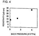
- Fig. 4 shows the relationship between the back pressure (pressure in a vacuum chamber in which deposition is started) and the resistivity of an electrode film in depositing the electrode film made of a refractory metal such as tungsten.
- the resistivity is 13.4 ⁇ cm at a back pressure of 1.10 x 10 -5 Pa, 16.4 ⁇ cm at a back pressure of 1.40 x 10 -4 Pa, and 32.5 ⁇ cm at a back pressure of 4.00 x 10 -4 Pa. It can be confirmed that the electric resistivity of the electrode film deposited under a pressure of 1 x 10 -4 Pa or more is higher than the electrical resistivity of the electrode film deposited under a pressure of about 1 x 10 -5 Pa or lower.
- deposition of an electrode film made of a refractory metal is conventionally started after the deposition chamber is evacuated to 3 x 10 -5 Pa or lower.
- a load lock system vacuum deposition apparatus is suitable for depositing an electrode film using a refractory metal under a high vacuum of 3 x 10 -5 Pa or less, as described above.
- a load lock system deposition apparatus has the disadvantage that the apparatus is expensive, and the number of the substrates that can be input per batch is small, thus increasing the deposition cost.
- a batch system vacuum deposition apparatus is inexpensive and is capable of processing a large number of substrates per batch.
- a batch system vacuum deposition apparatus requires being exposed to air each time a substrate is exchanged for a new substrate, and the time required for increasing the degree of vacuum increases as the degree of vacuum increases, thereby causing the problem of lengthening the exhaust time for deposition under 3 x 10 -5 Pa or less so as to greatly decrease the throughput and manufacturing efficiency.
- preferred embodiments of the present invention provide a method of forming an electrode film to produce an electrode film having low electrical resistivity even when a refractory metal is deposited under a back pressure of about 1 x 10 -4 Pa or more.
- a method of forming an electrode film includes starting deposition of a refractory metal such as tungsten, tantalum, or other suitable material on a substrate under a back pressure of about 1 x 10 -4 Pa to 5 x 10 -3 Pa, and then annealing the substrate on which the metal is deposited to decrease the electrical resistivity of the electrode film.
- a refractory metal such as tungsten, tantalum, or other suitable material
- the inventors of the present invention discovered that in the electrode film deposited under a pressure of about 1 x 10 -4 Pa or more, the increase in the electrical resistivity is caused by hydrogen and an oxide contained in the electrode film. It was also discovered that the hydrogen and oxide contained in the electrode film can be removed as water and hydrogen gas from the electrode film by annealing under vacuum, thereby decreasing the electrical resistivity of the electrode film.
- the resistivity can be decreased by annealing under vacuum, thereby decreasing an insertion loss and the deposition cost of the electrode film.
- vacuum annealing is performed to decrease resistivity, thereby decreasing the insertion loss of a resonator, a band-pass filter, or other component, and improving the efficiency of production thereof to decrease the deposition cost of an electrode film.
- a piezoelectric substrate 1 is first prepared.
- a commercial LiTaO 3 , LiNbO 3 , LiBi 4 O 7 , quartz crystal, or piezoelectric ceramics material can be used. Other substrates can also be used.
- the surface of the piezoelectric substrate 1 is cleaned by wet cleaning with a neutral detergent, an alcohol, or the like, or dry cleaning with oxygen plasma, or other suitable cleaning agent.
- a tungsten thin film 2 is then deposited over the entire surface of the piezoelectric substrate 1 preferably by using a batch system vacuum deposition apparatus or other suitable device.
- a vacuum deposition apparatus is generally used for deposition, a vacuum evaporation apparatus, a sputtering apparatus, or a CVD apparatus may be used, and the type of the apparatus used does not matter.
- deposition of the tungsten thin film 2 is started after the pressure in the vacuum chamber reaches the intended back pressure value, and Ar gas is introduced into the vacuum chamber so that deposition of the tungsten thin film 2 is performed under a pressure of about 0.4 Pa.
- deposition of the tungsten thin film 2 is preferably started under a back pressure of about 1 x 10 -4 Pa to about 5 x 10 -3 Pa.
- the piezoelectric substrate 1 is annealed under a vacuum of about 5 x 10 -3 Pa or less, as shown in Fig. 1C.
- Fig. 2 shows the results of measurement of the partial pressures of the hydrogen gas and water generated from the tungsten thin film 2 when the vacuum annealing temperature (heating temperature) was changed to near about 800°C.
- solid lines indicate the tungsten thin film deposited at a back pressure of about 4 x 10⁻⁴ Pa.
- Dotted lines in Fig. 2 indicate the results of the tungsten thin film deposited at a back pressure of about 1 x 10 -5 Pa.
- Fig. 2 shows that generation of hydrogen and water from the tungsten thin film 2 deposited at a back pressure of about 4 x 10 -4 Pa occurs at a temperature of about approximately 70°C to approximately 150°C.
- the tungsten thin film deposited at a back pressure of about 1 x 10 -5 Pa generates neither hydrogen nor water, substantially. It is to be noted that the partial pressure of the water is relatively great at the temperature more than about 100°C due to vaporization of water from the chamber of the measuring instrument.
- the tungsten thin film is annealed at a temperature of about 150°C or more so as to degas the tungsten thin film. It has been confirmed by the inventors that the vacuum annealing time is preferably about 30 minutes or more.
- a resist film 3 is formed over the entire surface of the tungsten thin film 2.
- the resist either of a commercial negative type and positive type can be used.
- the resist film 3 is exposed by using a patterning mask 4 and an exposure device, developed by a development device, and then dried to form the resist film 3 having a desired pattern and cured on the tungsten thin film 2, as shown in Fig. 1F.
- the exposed portion of the tungsten thin film 2 is etched off with an etchant which can selectively etch the tungsten thin film 2, as shown in Fig. 1G, and then the resist film 3 is separated to form an electrode film (tungsten thin film 2) having a desired pattern, as shown in Fig. 1H.
- Etching may be performed by dry etching with plasma without using the etchant.
- the transmission characteristics of an element portion for a resonator, a filter, or other component are confirmed to examine whether or not the desired frequency characteristics are obtained. If the desired frequency characteristics are obtained, the process moves on to the assembly step.
- the tungsten thin film 2 is annealed under a vacuum of about 5 x 10 -3 Pa or less to remove the hydrogen and/or oxide contained in the tungsten thin film 2 immediately after deposition, whereby the electrical resistivity can be decreased to the same level as a film deposited under a pressure of about 3 x 10 -5 Pa. Therefore, an electrode film having low electrical resistivity can be formed by vacuum annealing even when the film is deposited under relatively high pressure by using a batch system vacuum deposition apparatus or other suitable device, and an electrode film with a low insertion loss can be obtained at low cost.
Landscapes
- Chemical & Material Sciences (AREA)
- Engineering & Computer Science (AREA)
- Chemical Kinetics & Catalysis (AREA)
- Materials Engineering (AREA)
- Mechanical Engineering (AREA)
- Metallurgy (AREA)
- Organic Chemistry (AREA)
- General Chemical & Material Sciences (AREA)
- Physics & Mathematics (AREA)
- Thermal Sciences (AREA)
- Inorganic Chemistry (AREA)
- Manufacturing & Machinery (AREA)
- Physical Vapour Deposition (AREA)
- Piezo-Electric Or Mechanical Vibrators, Or Delay Or Filter Circuits (AREA)
- Chemical Vapour Deposition (AREA)
- Electrodes Of Semiconductors (AREA)
- Internal Circuitry In Semiconductor Integrated Circuit Devices (AREA)
- Surface Acoustic Wave Elements And Circuit Networks Thereof (AREA)
Abstract


Description
- The present invention relates to a method of forming an electrode film, and more particularly, to a method for decreasing the electrical resistivity of an electrode film for use with a resonator, a filter, or other electronic component.
- In a radio frequency resonator (surface acoustic wave device), a band-pass filter or other filter using a Love wave or shear horizontal ("SH") wave, a refractory metal is used to form an electrode film. The electrode film used for such application is required to have a low electrical resistivity, a high electromechanical coupling coefficient, and a high density. This is because the electrode film made of a refractory metal material is advantageous for suppressing deterioration in insertion loss when increasing the frequency of a device, as compared with other materials.
- It is known that when depositing such an electrode film made of a refractory metal on a piezoelectric substrate, the electrical resistivity of the electrode film rapidly increases depending upon pressure when deposition of the refractory metal is started at a back pressure of about 1 x 10⁻⁴ Pa in a deposition chamber. For example, Fig. 4 shows the relationship between the back pressure (pressure in a vacuum chamber in which deposition is started) and the resistivity of an electrode film in depositing the electrode film made of a refractory metal such as tungsten. In this example, the resistivity is 13.4 µΩ·cm at a back pressure of 1.10 x 10⁻⁵ Pa, 16.4 µΩ·cm at a back pressure of 1.40 x 10⁻⁴ Pa, and 32.5 µΩ·cm at a back pressure of 4.00 x 10⁻⁴ Pa. It can be confirmed that the electric resistivity of the electrode film deposited under a pressure of 1 x 10⁻⁴ Pa or more is higher than the electrical resistivity of the electrode film deposited under a pressure of about 1 x 10⁻⁵ Pa or lower.
- Therefore, deposition of an electrode film made of a refractory metal is conventionally started after the deposition chamber is evacuated to 3 x 10⁻⁵ Pa or lower.
- A load lock system vacuum deposition apparatus is suitable for depositing an electrode film using a refractory metal under a high vacuum of 3 x 10⁻⁵ Pa or less, as described above. However, such a load lock system deposition apparatus has the disadvantage that the apparatus is expensive, and the number of the substrates that can be input per batch is small, thus increasing the deposition cost.
- On the other hand, a batch system vacuum deposition apparatus is inexpensive and is capable of processing a large number of substrates per batch. However, such a batch system vacuum deposition apparatus requires being exposed to air each time a substrate is exchanged for a new substrate, and the time required for increasing the degree of vacuum increases as the degree of vacuum increases, thereby causing the problem of lengthening the exhaust time for deposition under 3 x 10⁻⁵ Pa or less so as to greatly decrease the throughput and manufacturing efficiency.
- In order to overcome the problems described above, preferred embodiments of the present invention provide a method of forming an electrode film to produce an electrode film having low electrical resistivity even when a refractory metal is deposited under a back pressure of about 1 x 10⁻⁴ Pa or more.
- According to one preferred embodiment of the present invention, a method of forming an electrode film includes starting deposition of a refractory metal such as tungsten, tantalum, or other suitable material on a substrate under a back pressure of about 1 x 10⁻⁴ Pa to 5 x 10⁻³ Pa, and then annealing the substrate on which the metal is deposited to decrease the electrical resistivity of the electrode film.
- It is conventionally thought that when deposition of a refractory metal is started under a pressure of about 1 x 10⁻⁴ Pa or more, the electrical resistivity of the electrode film is increased to be beyond the allowable range.
- As a result of intensive research of the cause for the increase in the electrical resistivity, the inventors of the present invention discovered that in the electrode film deposited under a pressure of about 1 x 10⁻⁴ Pa or more, the increase in the electrical resistivity is caused by hydrogen and an oxide contained in the electrode film. It was also discovered that the hydrogen and oxide contained in the electrode film can be removed as water and hydrogen gas from the electrode film by annealing under vacuum, thereby decreasing the electrical resistivity of the electrode film.
- Therefore, in accordance with preferred embodiments of the present invention, even when deposition is started under a pressure of about 1 x 10⁻⁴ Pa or more, the resistivity can be decreased by annealing under vacuum, thereby decreasing an insertion loss and the deposition cost of the electrode film.
- According to preferred embodiments of the present invention, after deposition is started at a back pressure of about 1 x 10⁻⁴ Pa to 5 x 10⁻³ Pa, vacuum annealing is performed to decrease resistivity, thereby decreasing the insertion loss of a resonator, a band-pass filter, or other component, and improving the efficiency of production thereof to decrease the deposition cost of an electrode film.
- Other features, steps, characteristics and advantages of the present invention will become apparent from the following detailed description of preferred embodiments of the present invention given with reference to the attached drawings.
- For the purpose of illustrating the present invention, there is shown in the drawings several forms that are presently preferred, it being understood, however, that the invention is not limited to the precise arrangements and instrumentalities shown.
-
- Figs. 1A to 1H are drawings illustrating a method of forming an electrode film in accordance with a preferred embodiment of the present invention.
- Fig. 2 is a graph showing the relationship between the vacuum annealing temperature (heating temperature) of a tungsten thin film and the partial pressures of the hydrogen gas and water generated from the tungsten thin films, which are deposited at about 4 x 10⁻⁴ Pa and about 1 x 10⁻⁵ Pa, respectively.
- Fig. 3A is a sectional view schematically showing the state of a tungsten thin film before vacuum annealing, and Fig. 3B is a sectional view schematically showing the state of the tungsten thin film after vacuum annealing.
- Fig. 4 is a graph showing the pressure (back pressure) in a vacuum chamber at the start of deposition and the resistivity of an electrode film.
-
- Hereinafter, preferred embodiments of the present invention are explained in detail with reference to the drawings.
- As shown in Fig. 1A, a
piezoelectric substrate 1 is first prepared. As thepiezoelectric substrate 1, a commercial LiTaO3, LiNbO3, LiBi4O7, quartz crystal, or piezoelectric ceramics material can be used. Other substrates can also be used. The surface of thepiezoelectric substrate 1 is cleaned by wet cleaning with a neutral detergent, an alcohol, or the like, or dry cleaning with oxygen plasma, or other suitable cleaning agent. - As shown in Fig. 1B, a tungsten
thin film 2 is then deposited over the entire surface of thepiezoelectric substrate 1 preferably by using a batch system vacuum deposition apparatus or other suitable device. Although the vacuum deposition apparatus is generally used for deposition, a vacuum evaporation apparatus, a sputtering apparatus, or a CVD apparatus may be used, and the type of the apparatus used does not matter. - In this deposition step, after the
piezoelectric substrate 1 is set in the vacuum chamber, the vacuum chamber is evacuated, deposition of the tungstenthin film 2 is started after the pressure in the vacuum chamber reaches the intended back pressure value, and Ar gas is introduced into the vacuum chamber so that deposition of the tungstenthin film 2 is performed under a pressure of about 0.4 Pa. However, deposition of the tungstenthin film 2 is preferably started under a back pressure of about 1 x 10⁻⁴ Pa to about 5 x 10⁻³ Pa. - After the tungsten
thin film 2 is formed on the surface of thepiezoelectric substrate 1, as described above, thepiezoelectric substrate 1 is annealed under a vacuum of about
5 x 10⁻³ Pa or less, as shown in Fig. 1C. - Fig. 2 shows the results of measurement of the partial pressures of the hydrogen gas and water generated from the tungsten
thin film 2 when the vacuum annealing temperature (heating temperature) was changed to near about 800°C. In Fig. 2, solid lines indicate the tungsten thin film deposited at a back pressure of about 4 x 10⁻⁴ Pa. Dotted lines in Fig. 2 indicate the results of the tungsten thin film deposited at a back pressure of about 1 x 10⁻⁵ Pa. Fig. 2 shows that generation of hydrogen and water from the tungstenthin film 2 deposited at a back pressure of about 4 x 10⁻⁴ Pa occurs at a temperature of about approximately 70°C to approximately 150°C. On the other hand, the tungsten thin film deposited at a back pressure of about 1 x 10⁻⁵ Pa generates neither hydrogen nor water, substantially. It is to be noted that the partial pressure of the water is relatively great at the temperature more than about 100°C due to vaporization of water from the chamber of the measuring instrument. - As is understood from Fig. 2, it is preferable that the tungsten thin film is annealed at a temperature of about 150°C or more so as to degas the tungsten thin film. It has been confirmed by the inventors that the vacuum annealing time is preferably about 30 minutes or more.
- After deposition of the tungsten
thin film 2 and before vacuum annealing, as schematically shown in Fig. 3A, anoxide 5 andhydrogen 6 were detected in the tungstenthin film 2. It is thought that theoxide 5 andhydrogen 6 will increase the resistance of the tungstenthin film 2. Therefore, as shown in Fig. 3B, the above-described vacuum annealing can escape theoxide 5 andhydrogen 6 as water and hydrogen in the tungstenthin film 2, thereby decreasing the electrical resistivity of the tungstenthin film 2. - After the tungsten
thin film 2 on the surface of thepiezoelectric substrate 1 is annealed under vacuum, as shown in Fig. 1D, a resistfilm 3 is formed over the entire surface of the tungstenthin film 2. As the resist, either of a commercial negative type and positive type can be used. As shown in Fig. 1E, the resistfilm 3 is exposed by using apatterning mask 4 and an exposure device, developed by a development device, and then dried to form the resistfilm 3 having a desired pattern and cured on the tungstenthin film 2, as shown in Fig. 1F. The exposed portion of the tungstenthin film 2 is etched off with an etchant which can selectively etch the tungstenthin film 2, as shown in Fig. 1G, and then the resistfilm 3 is separated to form an electrode film (tungsten thin film 2) having a desired pattern, as shown in Fig. 1H. Etching may be performed by dry etching with plasma without using the etchant. - Then, the transmission characteristics of an element portion for a resonator, a filter, or other component are confirmed to examine whether or not the desired frequency characteristics are obtained. If the desired frequency characteristics are obtained, the process moves on to the assembly step.
- In this way, the tungsten
thin film 2 is annealed under a vacuum of about 5 x 10⁻³ Pa or less to remove the hydrogen and/or oxide contained in the tungstenthin film 2 immediately after deposition, whereby the electrical resistivity can be decreased to the same level as a film deposited under a pressure of about 3 x 10⁻⁵ Pa. Therefore, an electrode film having low electrical resistivity can be formed by vacuum annealing even when the film is deposited under relatively high pressure by using a batch system vacuum deposition apparatus or other suitable device, and an electrode film with a low insertion loss can be obtained at low cost. - While preferred embodiments of the invention have been disclosed, various modes of carrying out the principles disclosed herein are contemplated as being within the scope of the following claims. Therefore, it is understood that the scope of the invention is not to be limited except as otherwise set forth in the claims.
Claims (13)
- A method of forming an electrode film using a vacuum deposition apparatus, the method comprising the steps of:depositing a refractory metal (2) on a substrate (1) after reaching a back pressure, in a deposition chamber, in a range of about 1 x 10⁻⁴ Pa to about 5 x 10⁻³ Pa; andannealing the refractory metal (2) to decrease the electrical resistivity of the electrode film.
- A method according to claim 1, wherein in the annealing step, the substrate (1) is kept at a temperature of about 100°C or more for approximately 30 minutes or more.
- A method according to claim 1 or 2, wherein the refractory metal (2) is one of tungsten and tantalum.
- A method according to claim 1, 2 or 3, wherein the substrate (1) is a piezoelectric substrate.
- A method according to claim 4, wherein the piezoelectric substrate (1) is made of one of LiTaO3, LiNbO3, LiBi4O7, quartz crystal, and piezoelectric ceramics material.
- A method according to any previous claim, wherein the refractory metal (2) is deposited over the entire surface of the substrate (1) using one of a batch system vacuum deposition apparatus, a vacuum evaporation apparatus, a sputtering apparatus, and a CVD apparatus.
- A method according to any previous claim, further comprising the step of introducing Ar gas into the deposition chamber so that deposition of the refractory metal (2) is performed under a pressure of about 0.4 Pa.
- A method according to any previous claim, wherein the step of annealing the refractory metal (2) is performed at a pressure of about 5 x 10⁻³ Pa or less.
- A method according to any previous claim, wherein the step of annealing the refractory metal (2) is performed at a temperature of about 150°C or more.
- A method according to any previous claim, further comprising the step of forming a resist film (3) over the entire surface of the refractory metal (2) after the annealing step.
- A method according to claim 10, wherein the resist film (3) is one of a negative type and a positive type.
- A method according to claim 10 or 11, further comprising the step of exposing the resist film (3) using a patterning mask (4) and an exposure device, developing the resist film and drying the resist film to produce a desired pattern.
- The method according to claim 12, further comprising the step of etching exposed portions of the refractory metal (2) to form an electrode film having a desired pattern.
Applications Claiming Priority (2)
| Application Number | Priority Date | Filing Date | Title |
|---|---|---|---|
| JP2000148853 | 2000-05-19 | ||
| JP2000148853A JP3651360B2 (en) | 2000-05-19 | 2000-05-19 | Method for forming electrode film |
Publications (3)
| Publication Number | Publication Date |
|---|---|
| EP1156132A2 true EP1156132A2 (en) | 2001-11-21 |
| EP1156132A3 EP1156132A3 (en) | 2005-02-02 |
| EP1156132B1 EP1156132B1 (en) | 2009-07-01 |
Family
ID=18654810
Family Applications (1)
| Application Number | Title | Priority Date | Filing Date |
|---|---|---|---|
| EP20010401316 Expired - Lifetime EP1156132B1 (en) | 2000-05-19 | 2001-05-21 | Method of forming electrode film |
Country Status (4)
| Country | Link |
|---|---|
| US (1) | US6581258B2 (en) |
| EP (1) | EP1156132B1 (en) |
| JP (1) | JP3651360B2 (en) |
| DE (1) | DE60139100D1 (en) |
Cited By (9)
| Publication number | Priority date | Publication date | Assignee | Title |
|---|---|---|---|---|
| US9613818B2 (en) | 2015-05-27 | 2017-04-04 | Lam Research Corporation | Deposition of low fluorine tungsten by sequential CVD process |
| US9653353B2 (en) | 2009-08-04 | 2017-05-16 | Novellus Systems, Inc. | Tungsten feature fill |
| US9673146B2 (en) | 2009-04-16 | 2017-06-06 | Novellus Systems, Inc. | Low temperature tungsten film deposition for small critical dimension contacts and interconnects |
| US9754824B2 (en) | 2015-05-27 | 2017-09-05 | Lam Research Corporation | Tungsten films having low fluorine content |
| US9953984B2 (en) | 2015-02-11 | 2018-04-24 | Lam Research Corporation | Tungsten for wordline applications |
| US9978605B2 (en) | 2015-05-27 | 2018-05-22 | Lam Research Corporation | Method of forming low resistivity fluorine free tungsten film without nucleation |
| US10256142B2 (en) | 2009-08-04 | 2019-04-09 | Novellus Systems, Inc. | Tungsten feature fill with nucleation inhibition |
| US11348795B2 (en) | 2017-08-14 | 2022-05-31 | Lam Research Corporation | Metal fill process for three-dimensional vertical NAND wordline |
| US11549175B2 (en) | 2018-05-03 | 2023-01-10 | Lam Research Corporation | Method of depositing tungsten and other metals in 3D NAND structures |
Families Citing this family (11)
| Publication number | Priority date | Publication date | Assignee | Title |
|---|---|---|---|---|
| US9076843B2 (en) | 2001-05-22 | 2015-07-07 | Novellus Systems, Inc. | Method for producing ultra-thin tungsten layers with improved step coverage |
| US7052117B2 (en) | 2002-07-03 | 2006-05-30 | Dimatix, Inc. | Printhead having a thin pre-fired piezoelectric layer |
| US8491076B2 (en) | 2004-03-15 | 2013-07-23 | Fujifilm Dimatix, Inc. | Fluid droplet ejection devices and methods |
| US7281778B2 (en) | 2004-03-15 | 2007-10-16 | Fujifilm Dimatix, Inc. | High frequency droplet ejection device and method |
| EP1836056B1 (en) | 2004-12-30 | 2018-11-07 | Fujifilm Dimatix, Inc. | Ink jet printing |
| US7988247B2 (en) | 2007-01-11 | 2011-08-02 | Fujifilm Dimatix, Inc. | Ejection of drops having variable drop size from an ink jet printer |
| US9159571B2 (en) | 2009-04-16 | 2015-10-13 | Lam Research Corporation | Tungsten deposition process using germanium-containing reducing agent |
| US8853080B2 (en) | 2012-09-09 | 2014-10-07 | Novellus Systems, Inc. | Method for depositing tungsten film with low roughness and low resistivity |
| US9153486B2 (en) | 2013-04-12 | 2015-10-06 | Lam Research Corporation | CVD based metal/semiconductor OHMIC contact for high volume manufacturing applications |
| US9589808B2 (en) | 2013-12-19 | 2017-03-07 | Lam Research Corporation | Method for depositing extremely low resistivity tungsten |
| US9997405B2 (en) | 2014-09-30 | 2018-06-12 | Lam Research Corporation | Feature fill with nucleation inhibition |
Citations (5)
| Publication number | Priority date | Publication date | Assignee | Title |
|---|---|---|---|---|
| GB1214698A (en) * | 1967-10-17 | 1970-12-02 | Gen Electric | Improvements in b tungsten resistor films and method of forming |
| US5677240A (en) * | 1992-07-21 | 1997-10-14 | Semiconductor Energy Laboratory Co., Ltd. | Method for forming a semiconductor device |
| US6033542A (en) * | 1993-07-27 | 2000-03-07 | Kabushiki Kaisha Kobe Seiko Sho | Electrode and its fabrication method for semiconductor devices, and sputtering target for forming electrode film for semiconductor devices |
| US6057628A (en) * | 1997-12-01 | 2000-05-02 | Board Of Regents Of The University Of Nebraska | Piezoelectric sensors/actuators for use in refractory environments |
| US6107199A (en) * | 1998-10-24 | 2000-08-22 | International Business Machines Corporation | Method for improving the morphology of refractory metal thin films |
Family Cites Families (1)
| Publication number | Priority date | Publication date | Assignee | Title |
|---|---|---|---|---|
| JP3266195B2 (en) * | 1999-03-23 | 2002-03-18 | 日本電気株式会社 | Method for manufacturing semiconductor device |
-
2000
- 2000-05-19 JP JP2000148853A patent/JP3651360B2/en not_active Expired - Lifetime
-
2001
- 2001-05-08 US US09/851,063 patent/US6581258B2/en not_active Expired - Lifetime
- 2001-05-21 EP EP20010401316 patent/EP1156132B1/en not_active Expired - Lifetime
- 2001-05-21 DE DE60139100T patent/DE60139100D1/en not_active Expired - Lifetime
Patent Citations (5)
| Publication number | Priority date | Publication date | Assignee | Title |
|---|---|---|---|---|
| GB1214698A (en) * | 1967-10-17 | 1970-12-02 | Gen Electric | Improvements in b tungsten resistor films and method of forming |
| US5677240A (en) * | 1992-07-21 | 1997-10-14 | Semiconductor Energy Laboratory Co., Ltd. | Method for forming a semiconductor device |
| US6033542A (en) * | 1993-07-27 | 2000-03-07 | Kabushiki Kaisha Kobe Seiko Sho | Electrode and its fabrication method for semiconductor devices, and sputtering target for forming electrode film for semiconductor devices |
| US6057628A (en) * | 1997-12-01 | 2000-05-02 | Board Of Regents Of The University Of Nebraska | Piezoelectric sensors/actuators for use in refractory environments |
| US6107199A (en) * | 1998-10-24 | 2000-08-22 | International Business Machines Corporation | Method for improving the morphology of refractory metal thin films |
Cited By (12)
| Publication number | Priority date | Publication date | Assignee | Title |
|---|---|---|---|---|
| US9673146B2 (en) | 2009-04-16 | 2017-06-06 | Novellus Systems, Inc. | Low temperature tungsten film deposition for small critical dimension contacts and interconnects |
| US9653353B2 (en) | 2009-08-04 | 2017-05-16 | Novellus Systems, Inc. | Tungsten feature fill |
| US10103058B2 (en) | 2009-08-04 | 2018-10-16 | Novellus Systems, Inc. | Tungsten feature fill |
| US10256142B2 (en) | 2009-08-04 | 2019-04-09 | Novellus Systems, Inc. | Tungsten feature fill with nucleation inhibition |
| US9953984B2 (en) | 2015-02-11 | 2018-04-24 | Lam Research Corporation | Tungsten for wordline applications |
| US10529722B2 (en) | 2015-02-11 | 2020-01-07 | Lam Research Corporation | Tungsten for wordline applications |
| US9613818B2 (en) | 2015-05-27 | 2017-04-04 | Lam Research Corporation | Deposition of low fluorine tungsten by sequential CVD process |
| US9754824B2 (en) | 2015-05-27 | 2017-09-05 | Lam Research Corporation | Tungsten films having low fluorine content |
| US9978605B2 (en) | 2015-05-27 | 2018-05-22 | Lam Research Corporation | Method of forming low resistivity fluorine free tungsten film without nucleation |
| US10546751B2 (en) | 2015-05-27 | 2020-01-28 | Lam Research Corporation | Forming low resistivity fluorine free tungsten film without nucleation |
| US11348795B2 (en) | 2017-08-14 | 2022-05-31 | Lam Research Corporation | Metal fill process for three-dimensional vertical NAND wordline |
| US11549175B2 (en) | 2018-05-03 | 2023-01-10 | Lam Research Corporation | Method of depositing tungsten and other metals in 3D NAND structures |
Also Published As
| Publication number | Publication date |
|---|---|
| US20010042290A1 (en) | 2001-11-22 |
| US6581258B2 (en) | 2003-06-24 |
| JP2001329365A (en) | 2001-11-27 |
| EP1156132B1 (en) | 2009-07-01 |
| EP1156132A3 (en) | 2005-02-02 |
| DE60139100D1 (en) | 2009-08-13 |
| JP3651360B2 (en) | 2005-05-25 |
Similar Documents
| Publication | Publication Date | Title |
|---|---|---|
| US6581258B2 (en) | Method of forming electrode film | |
| US5780713A (en) | Post-fabrication tuning of acoustic resonators | |
| US5348617A (en) | Selective etching process | |
| JPH07169751A (en) | Simultaneous removal of photoresist and polysilicon/polycide | |
| US6686675B2 (en) | Electronic device and method for producing the same | |
| WO2024001087A1 (en) | Preparation method for film bulk acoustic resonator, and film bulk acoustic resonator | |
| EP1467483A2 (en) | Method for manufacturing a surface acoustic wave device | |
| JP3293564B2 (en) | Manufacturing method of electronic device | |
| US6306313B1 (en) | Selective etching of thin films | |
| JP2007336417A (en) | Surface acoustic wave element and manufacturing method thereof | |
| JPH0294911A (en) | Manufacture of surface acoustic wave element | |
| CN112436815B (en) | Temperature-compensated surface acoustic wave device and method of manufacturing the same | |
| US20040195684A1 (en) | Method for making a radio frequency component and component produced thereby | |
| US6725513B2 (en) | Method for manufacturing surface acoustic wave apparatus | |
| JP2024000433A (en) | Deposition method and elastic wave device | |
| JP2568551B2 (en) | Manufacturing method of surface acoustic wave device | |
| JPH05109673A (en) | Manufacture of semiconductor device | |
| RU2079865C1 (en) | Method for making relief patterns in dielectric substrates | |
| JP2002184698A (en) | Method of manufacturing electronic component | |
| JP3716431B2 (en) | SAW device manufacturing method | |
| JPS63314906A (en) | Manufacture of surface acoustic wave device | |
| KR100701367B1 (en) | Method for making capacitor mim in semiconductor | |
| JP2001066450A (en) | Method for production of glass waveguide | |
| JP2000341067A (en) | Method and device for adjusting frequency of piezoelectric device | |
| JPH0774573A (en) | Method for adjusting frequency of surface acoustic wave element |
Legal Events
| Date | Code | Title | Description |
|---|---|---|---|
| PUAI | Public reference made under article 153(3) epc to a published international application that has entered the european phase |
Free format text: ORIGINAL CODE: 0009012 |
|
| 17P | Request for examination filed |
Effective date: 20010526 |
|
| AK | Designated contracting states |
Kind code of ref document: A2 Designated state(s): AT BE CH CY DE DK ES FI FR GB GR IE IT LI LU MC NL PT SE TR |
|
| AX | Request for extension of the european patent |
Free format text: AL;LT;LV;MK;RO;SI |
|
| PUAL | Search report despatched |
Free format text: ORIGINAL CODE: 0009013 |
|
| AK | Designated contracting states |
Kind code of ref document: A3 Designated state(s): AT BE CH CY DE DK ES FI FR GB GR IE IT LI LU MC NL PT SE TR |
|
| AX | Request for extension of the european patent |
Extension state: AL LT LV MK RO SI |
|
| RIC1 | Information provided on ipc code assigned before grant |
Ipc: 7C 23C 14/58 B Ipc: 7C 23C 14/18 A Ipc: 7H 01L 21/768 B Ipc: 7H 01L 21/285 B Ipc: 7C 23C 16/06 B Ipc: 7H 01L 21/3205 B Ipc: 7C 23C 16/56 B Ipc: 7H 03H 3/08 B |
|
| AKX | Designation fees paid |
Designated state(s): DE FR GB |
|
| 17Q | First examination report despatched |
Effective date: 20070601 |
|
| RAP1 | Party data changed (applicant data changed or rights of an application transferred) |
Owner name: MURATA MANUFACTURING CO., LTD. |
|
| GRAP | Despatch of communication of intention to grant a patent |
Free format text: ORIGINAL CODE: EPIDOSNIGR1 |
|
| GRAS | Grant fee paid |
Free format text: ORIGINAL CODE: EPIDOSNIGR3 |
|
| GRAA | (expected) grant |
Free format text: ORIGINAL CODE: 0009210 |
|
| AK | Designated contracting states |
Kind code of ref document: B1 Designated state(s): DE FR GB |
|
| REG | Reference to a national code |
Ref country code: GB Ref legal event code: FG4D |
|
| REF | Corresponds to: |
Ref document number: 60139100 Country of ref document: DE Date of ref document: 20090813 Kind code of ref document: P |
|
| PLBE | No opposition filed within time limit |
Free format text: ORIGINAL CODE: 0009261 |
|
| STAA | Information on the status of an ep patent application or granted ep patent |
Free format text: STATUS: NO OPPOSITION FILED WITHIN TIME LIMIT |
|
| 26N | No opposition filed |
Effective date: 20100406 |
|
| GBPC | Gb: european patent ceased through non-payment of renewal fee |
Effective date: 20100521 |
|
| REG | Reference to a national code |
Ref country code: FR Ref legal event code: ST Effective date: 20110131 |
|
| PG25 | Lapsed in a contracting state [announced via postgrant information from national office to epo] |
Ref country code: FR Free format text: LAPSE BECAUSE OF NON-PAYMENT OF DUE FEES Effective date: 20100531 |
|
| PG25 | Lapsed in a contracting state [announced via postgrant information from national office to epo] |
Ref country code: GB Free format text: LAPSE BECAUSE OF NON-PAYMENT OF DUE FEES Effective date: 20100521 |
|
| PGFP | Annual fee paid to national office [announced via postgrant information from national office to epo] |
Ref country code: DE Payment date: 20200520 Year of fee payment: 20 |
|
| REG | Reference to a national code |
Ref country code: DE Ref legal event code: R071 Ref document number: 60139100 Country of ref document: DE |