EP1162683A2 - Scalable RF, N x M switching matrix architecture - Google Patents
Scalable RF, N x M switching matrix architecture Download PDFInfo
- Publication number
- EP1162683A2 EP1162683A2 EP01304978A EP01304978A EP1162683A2 EP 1162683 A2 EP1162683 A2 EP 1162683A2 EP 01304978 A EP01304978 A EP 01304978A EP 01304978 A EP01304978 A EP 01304978A EP 1162683 A2 EP1162683 A2 EP 1162683A2
- Authority
- EP
- European Patent Office
- Prior art keywords
- switch
- switching matrix
- architecture
- impedance
- matrix architecture
- Prior art date
- Legal status (The legal status is an assumption and is not a legal conclusion. Google has not performed a legal analysis and makes no representation as to the accuracy of the status listed.)
- Granted
Links
Images


Classifications
-
- H—ELECTRICITY
- H01—ELECTRIC ELEMENTS
- H01P—WAVEGUIDES; RESONATORS, LINES, OR OTHER DEVICES OF THE WAVEGUIDE TYPE
- H01P1/00—Auxiliary devices
- H01P1/10—Auxiliary devices for switching or interrupting
- H01P1/15—Auxiliary devices for switching or interrupting by semiconductor devices
Definitions
- the present invention relates generally to RF circuit switching architectures and, more particularly, to non-blocking, N x M switching matrices.
- each of the power dividers D 1 , D 2 , D 3 , and D 4 are configured to receive a corresponding RF signal input at input ports designated RF in 1, RF in 2, RF in N-1, and RF in N, respectively.
- the RF input signal is directed to output paths 1-M.
- These paths are then switched in and out using 1 x N switches, indicated generally at S 1 , S 2 , S 3 , and S N , disposed at the outputs, indicated generally at RF out 1, RF out 2, RF out N-1, and RF out N.
- a principal disadvantage of the arrangement shown in FIG. 1 is that the power dividers are frequency limited. Additionally, routing every RF input signal over plural paths to reach the corresponding switch simultaneously establishes multiple leakage paths for each input. This opportunity for isolation degradation is, consequently, multiplied by the number of splits on each input. Moreover, as a consequence of this multiple stage architecture, the input paths must be routed in a fashion which creates numerous cross over points, only some of these being identified by reference numeral CO in FIG. 1. The inability to provide adequate isolation between the input signal lines has made the above-described approach wholly impractical and unsuited to implementation as a discrete IC.
- PCB printed circuit board
- the scalable N x M switching matrix architecture of the present invention is characterized by a readily calculable number of cross over locations so that leakage can be accurately modeled and predicted.
- a scalable N x M switching matrix architecture is characterized by a readily calculable number of crossover locations and comprises one or more single pole, N throw ("SPNT") switches and, for each such switch, an N state impedance converter/amplitude compensation network.
- SPNT single pole, N throw
- each SPNT switch network selects the output to any of the N inputs in any combination with up to all N inputs being selected on.
- the individual 1 x N networks formed by each combination of SPNT switch and its corresponding impedance converter/amplitude compensation network comprises the N x M network.
- each SPNT switch In all switch conditions, the impedance and insertion loss of each SPNT switch is maintained by an impedance converter/amplitude compensation network.
- the number of output ports determines the number (M) of 1 x N networks in the matrix.
- the number of input ports is set by the number of legs (N) in the SPNT switch.
- a 1 x N switch network 10 for use in an N x M switching matrix architecture according to the present invention, which provides not only 1 x N switching connectivity, but also impedance and gain compensation regardless of the number of ports selected to be output.
- Each switch, S 1 through S N is directly controlled by embedded control logic 12 located on the same integrated circuit chip (IC) as the other components of the network 10.
- Impedance and/or gain compensation which may, as in the illustrative embodiment depicted in FIGS. 2-3D, be variable to permit multiple ports to be selected to a single output simultaneously, is performed by discrete impedance and gain compensation circuit modules indicated generally at G in 1 through G in N and G out .
- the present invention utilizes switched impedance circuitry to maintain constant, wide band port impedance and insertion gain.
- External driver circuitry is not needed because all of the logic is preferably incorporated on a single IC.
- the IC uses different combinations of internal impedance blocks to maintain constant match and gain.
- FIGS. 3A-3D Several illustrative topologies, in which the impedance blocks are arranged to achieve the flexibility and functionality required to implement a non-blocking N x M switch architecture in accordance with the present invention, are shown in FIGS. 3A-3D.
- each of these topologies uses a parallel path method for creating the attenuation steps. That is, instead of “daisy chaining" multiple attenuators, each with a bypass transistor for use when that stage is not desired, a "PI", "T” or other equivalent structure as shown in FIGS. 3A-3D is made with parallel resistive elements. This results in superior return loss and lower reference insertion loss as compared to conventional multi-step attenuator design approaches. Note that an ideal multistep attenuator would have no reference insertion loss. For example, a 5 dB multistep attenuator would be expected to have steps between 0 and 5 dB attenuation.
- bypass transistors In reality, there is loss in each bypass stage, so the conventional approach using bypass transistors would typically have been characterized by a reference insertion loss of 1.5 dB.
- the parallel method is therefore especially preferred for use in conjunction with implementing 1 x N switch networks in accordance with the present invention since the reference loss is significantly reduced in comparison to the conventional bypass transistor approach.
- the effect of switching multiple impedance in parallel or in series gives a varied overall input and output impedance, as well as varied insertion gain.
- the individual impedance are chosen so that appropriate lumped impedance are acquired for each desired state. These can be any combination of resistance, capacitance and inductance to get the requisite values.
- the illustrative topologies may be used individually or in any combination as required for the specific system impedance of a particular application. That is, the precise topology used will be based upon the particular impedance and loss requirements of each application.
- a specific combination of impedance is used for each port or combination of ports selected by SPNT switch SW under the direction of embedded logic control 12 (FIG. 2). Accordingly, the invention permits operation with more than one system impedance without degradation of performance.
- An external control word may be used to specify the system impedance so that the embedded control logic 12 (FIG. 2) can implement multiple sets of impedance combinations.
- a single component as network 10 may be used to function in a wide variety of impedance networks.
- a serial control interface is used to reduce the number of needed control lines.
- the device can be implemented in an addressable configuration, so that multiple serial devices can be on the same serial bus yet maintain individual device control, greatly simplifying the higher level assembly of the IC.
- FIGS. 4A-4C several non-blocking configurations employing the above-described 1 x N switching network element 10 will now be described.
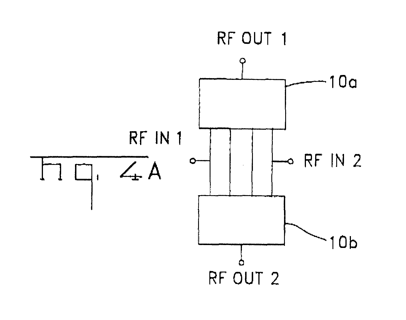
- FIG. 4A for example, there is shown a 2 x 2 non-blocking switch matrix architecture comprising two 1 x N switching networks indicated generally at 10a and 10b.
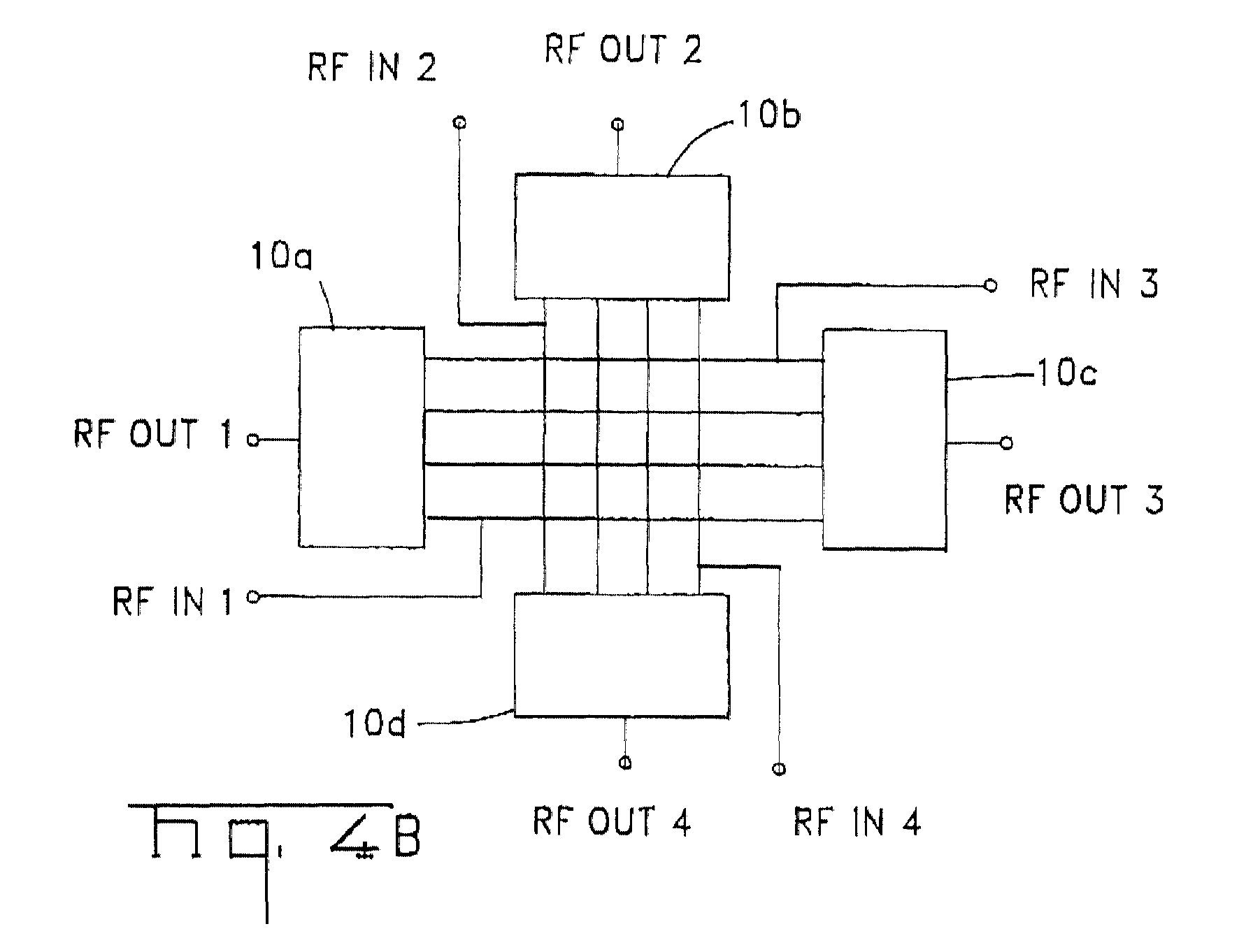
- FIG. 4B a 4 x 4 non-blocking switch matrix architecture is depicted, the structure using four 1 x N switching networks indicated generally at 10a, 10b, 10c and 10d.
- FIG. 4C there is shown yet another example of a non-blocking switch matrix architecture constructed in accordance with the present invention, this time employing six 1 x N switching networks indicated generally at 10a, 10b, 10c, 10d, 10e and 10f.
- the SPNT switch SW of each 1 x N network can select the output to any of the N inputs in any combination with up to all N inputs being selected on.
- N would be 2, 4 and 4, respectively.
- the impedance and the insertion loss of the switch is maintained by the impedance converter/amplitude compensation network comprising gain modules G in -1 through G in -N and G out (FIG 2).
- each switch element 10a-10f being aligned such that the inputs are directed towards each other and interconnected in a grid fashion.
- the RF portion of each switch element is identical, but the input port selected for any given control word can be controlled by a control logic block.
- the layout of the matrix is optimized such that the number of crossovers is minimized to maximize the overall isolation performance of the matrix.
- CX N 2- -N
- the number of crossovers depends on the configuration but can be easily calculated.
- CX (N*SE x )*((N-1)*SE y )
- SE x is the number of switch elements in the X direction
- SE y is the number of switch elements in the Y direction (see FIG. 5).
- the number of crossovers associated with each switch leg is the number of crossovers associated with each switch leg.
- the number of crossovers is kept constant for each input.
- the predictability of the RF matrix of the present invention enables it to be accurately simulated using a variety of ubiquitous commercial RF CAD tools so that the operating performance can be readily simulated and characterized.
Landscapes
- Electronic Switches (AREA)
- Analogue/Digital Conversion (AREA)
Abstract
Description
- The present invention relates generally to RF circuit switching architectures and, more particularly, to non-blocking, N x M switching matrices.
- A conventional approach to realizing a non-blocking N x M switching matrix in RF frequency applications is shown in FIG. 1 of the accompanying drawings. As seen in FIG. 1, each of the power dividers D1, D2, D3, and D4 are configured to receive a corresponding RF signal input at input ports designated
RF in1,RF in2, RFinN-1, and RFinN, respectively. At each power divider, the RF input signal is directed to output paths 1-M. These paths are then switched in and out using 1 x N switches, indicated generally at S1, S2, S3, and SN, disposed at the outputs, indicated generally atRF out1,RF out2, RFoutN-1, and RFoutN. - A principal disadvantage of the arrangement shown in FIG. 1 is that the power dividers are frequency limited. Additionally, routing every RF input signal over plural paths to reach the corresponding switch simultaneously establishes multiple leakage paths for each input. This opportunity for isolation degradation is, consequently, multiplied by the number of splits on each input. Moreover, as a consequence of this multiple stage architecture, the input paths must be routed in a fashion which creates numerous cross over points, only some of these being identified by reference numeral CO in FIG. 1. The inability to provide adequate isolation between the input signal lines has made the above-described approach wholly impractical and unsuited to implementation as a discrete IC. While it might be possible to construct a multiple layer printed circuit board (PCB) with shielded ground planes between layers to minimize cross talk and achieve acceptable isolation between signal paths, given the complexity of routing the paths in such a device, it is presently not possible to simulate or predict what level of isolation will be achieved until such a device were actually constructed and tested. In any event, it is believed that adapting the above-described matrix architecture to the ever-increasing numbers of inputs and outputs demanded by modern applications would pose substantial reliability concerns.
- The aforementioned deficiencies are addressed, and an advance is made in the art, by a switching architecture having the advantages of broad bandwidth, high isolation, and an ability to be implemented at the IC level due to a systematic approach taken to ensure isolation.
- The scalable N x M switching matrix architecture of the present invention is characterized by a readily calculable number of cross over locations so that leakage can be accurately modeled and predicted. A scalable N x M switching matrix architecture is characterized by a readily calculable number of crossover locations and comprises one or more single pole, N throw ("SPNT") switches and, for each such switch, an N state impedance converter/amplitude compensation network. In accordance with the present invention, each SPNT switch network selects the output to any of the N inputs in any combination with up to all N inputs being selected on. Collectively, the individual 1 x N networks formed by each combination of SPNT switch and its corresponding impedance converter/amplitude compensation network comprises the N x M network.
- In all switch conditions, the impedance and insertion loss of each SPNT switch is maintained by an impedance converter/amplitude compensation network. The number of output ports determines the number (M) of 1 x N networks in the matrix. The number of input ports is set by the number of legs (N) in the SPNT switch. By placing the SPNT switch as the last element before the output, the number of cross over points is maintained at a number which can be readily calculated based on the number of inputs and outputs.
- Illustrative embodiments of the invention will now be described, by way of example, with reference to the accompanying drawings in which like numerals refer to like parts and further and in which:
- FIG. 1 is a block diagram depicting a conventional non-blocking N x M switching matrix suitable for only a relatively small number of RF signal inputs and not adaptable for implementation as an integrated circuit;
- FIG. 2 is a block diagram schematic of a novel individual 1 x N switch network element for use with the present invention;
- FIGS. 3A-3D are circuit schematics depicting various topologies for obtaining impedance and gain compensation in the present invention;
- FIGS. 4A-4C are block diagrams respectively depicting illustrative configurations of non-blocking 2 x 2, 4 x 4, and 4 x 6 switch matrix architectures constructed in accordance with the present invention; and
- FIG. 5 depicts a non-blocking N x M switching matrix architecture constructed in accordance with the present invention and in which each switch element is aligned such that the inputs are directed towards each other and interconnected in a grid fashion.
-
- With initial reference to FIG. 2, there is shown a 1 x
N switch network 10, for use in an N x M switching matrix architecture according to the present invention, which provides not only 1 x N switching connectivity, but also impedance and gain compensation regardless of the number of ports selected to be output. Each switch, S1 through SN, is directly controlled by embeddedcontrol logic 12 located on the same integrated circuit chip (IC) as the other components of thenetwork 10. Impedance and/or gain compensation, which may, as in the illustrative embodiment depicted in FIGS. 2-3D, be variable to permit multiple ports to be selected to a single output simultaneously, is performed by discrete impedance and gain compensation circuit modules indicated generally atG in1 through GinN and Gout. - Initially, it should be noted that conventional 1 x N switches have several limitations which make them unsuitable for the non-blocking architecture contemplated by the inventors herein. First, such devices require many control lines, leading to complex routing requirements and user interface. Second, if multiple ports are switched to the same port simultaneously, the impedance seen at the ports gets lower and lower, proportional to the number of ports selected. Not only does the port impedance vary dramatically, the insertion gain varies significantly as well. Needless to say, it is undesirable to have such variations. Current switch matrix solutions also require multiple die and driver integrated circuits within a complex and costly package. As well, they are limited in their ability to maintain constant insertion and return loss through different switch states. Heretofore, switches have been designed to operate in a single system impedance environment, requiring multiple versions of the switch and external components to operate with proper impedance in systems of variable impedance.
- The present invention, on the other hand, utilizes switched impedance circuitry to maintain constant, wide band port impedance and insertion gain. External driver circuitry is not needed because all of the logic is preferably incorporated on a single IC. Advantageously, the IC uses different combinations of internal impedance blocks to maintain constant match and gain. Several illustrative topologies, in which the impedance blocks are arranged to achieve the flexibility and functionality required to implement a non-blocking N x M switch architecture in accordance with the present invention, are shown in FIGS. 3A-3D.
- Preferably, each of these topologies uses a parallel path method for creating the attenuation steps. That is, instead of "daisy chaining" multiple attenuators, each with a bypass transistor for use when that stage is not desired, a "PI", "T" or other equivalent structure as shown in FIGS. 3A-3D is made with parallel resistive elements. This results in superior return loss and lower reference insertion loss as compared to conventional multi-step attenuator design approaches. Note that an ideal multistep attenuator would have no reference insertion loss. For example, a 5 dB multistep attenuator would be expected to have steps between 0 and 5 dB attenuation. In reality, there is loss in each bypass stage, so the conventional approach using bypass transistors would typically have been characterized by a reference insertion loss of 1.5 dB. The parallel method is therefore especially preferred for use in conjunction with implementing 1 x N switch networks in accordance with the present invention since the reference loss is significantly reduced in comparison to the conventional bypass transistor approach.
- As will be readily appreciated by those skilled in the art, the effect of switching multiple impedance in parallel or in series gives a varied overall input and output impedance, as well as varied insertion gain. The individual impedance are chosen so that appropriate lumped impedance are acquired for each desired state. These can be any combination of resistance, capacitance and inductance to get the requisite values. By varying these impedances and gains, it is possible to offset the variation that would otherwise exist in a switch without this impedance/gain control. With such offsets, the device can maintain a constant input and output impedance and overall port to port gain.
- In any event, and with continued reference to FIGS. 3A-3D, it will be appreciated that the illustrative topologies may be used individually or in any combination as required for the specific system impedance of a particular application. That is, the precise topology used will be based upon the particular impedance and loss requirements of each application. For each port or combination of ports selected by SPNT switch SW under the direction of embedded logic control 12 (FIG. 2), a specific combination of impedance is used. Accordingly, the invention permits operation with more than one system impedance without degradation of performance. An external control word may be used to specify the system impedance so that the embedded control logic 12 (FIG. 2) can implement multiple sets of impedance combinations. As such, a single component as
network 10 may be used to function in a wide variety of impedance networks. - Preferably, a serial control interface is used to reduce the number of needed control lines. The device can be implemented in an addressable configuration, so that multiple serial devices can be on the same serial bus yet maintain individual device control, greatly simplifying the higher level assembly of the IC.
- In any event, and with particular reference now to FIGS. 4A-4C, several non-blocking configurations employing the above-described 1 x N
switching network element 10 will now be described. In FIG. 4A, for example, there is shown a 2 x 2 non-blocking switch matrix architecture comprising two 1 x N switching networks indicated generally at 10a and 10b. In FIG. 4B, a 4 x 4 non-blocking switch matrix architecture is depicted, the structure using four 1 x N switching networks indicated generally at 10a, 10b, 10c and 10d. In FIG. 4C, there is shown yet another example of a non-blocking switch matrix architecture constructed in accordance with the present invention, this time employing six 1 x N switching networks indicated generally at 10a, 10b, 10c, 10d, 10e and 10f. - Under the control of embedded control logic 12 (FIG. 2), the SPNT switch SW of each 1 x N network, as
network 10a, can select the output to any of the N inputs in any combination with up to all N inputs being selected on. In the preceding embodiments depicted in FIGS. 4A-4C, N would be 2, 4 and 4, respectively. In all switch conditions, the impedance and the insertion loss of the switch is maintained by the impedance converter/amplitude compensation network comprising gain modules Gin-1 through Gin-N and Gout (FIG 2). - A generalized case, i.e., an N x M architecture is depicted in FIG. 5 with each
switch element 10a-10f being aligned such that the inputs are directed towards each other and interconnected in a grid fashion. The RF portion of each switch element is identical, but the input port selected for any given control word can be controlled by a control logic block. Hence, the layout of the matrix is optimized such that the number of crossovers is minimized to maximize the overall isolation performance of the matrix. - For a symmetrical switch matrix in which the number of inputs is equal to the number of outputs (i.e., N=M), the minimum number of crossovers (CX) in the matrix is given by the relation:
- Just as important as the total number of crossovers is the number of crossovers associated with each switch leg. Preferably, the number of crossovers is kept constant for each input. By designing the architecture such that each associated input has the same number of crossovers, it is possible to ensure that each input is equally loaded. Advantageously, the predictability of the RF matrix of the present invention enables it to be accurately simulated using a variety of ubiquitous commercial RF CAD tools so that the operating performance can be readily simulated and characterized.
Claims (9)
- A scalable, non-blocking N x M switching matrix architecture having a minimum number of crossovers (CX) in the matrix represented by the following equation:with the proviso that when N=M, CX = N2-NN is the number of inputs in the matrix;M is the number of outputs in the matrix;SEx is the number of switch elements in the X direction; andSEy is the number of switch elements in the Y direction;
- The switching matrix architecture of claim 1, wherein the architecture comprises at least one single pole, N throw switch and, for each such switch, an N state impedance converter/amplitude compensation network.
- The switching matrix architecture of claim 2, wherein the N state impedance converter/ amplitude compensation network comprises impedance and gain compensation circuit modules.
- The switching matrix architecture of claim 3, wherein the modules are arranged in a topology that utilizes a parallel path method for creating attenuation steps.
- The switching matrix architecture of claim 3, wherein the modules are selected and arranged to maintain constant input and output impedance and overall port-to-port gain.
- The switching matrix architecture of claim 2, wherein each switch network selects the output to any of the N inputs in any combination with up to all N inputs being selected on.
- The switching matrix architecture of claim 2, wherein each switch is directly controlled by embedded control logic.
- The switching matrix architecture of claim 2, wherein
- The switching matrix architecture of claim 1, wherein the number of crossovers for each input is kept constant.
Applications Claiming Priority (2)
| Application Number | Priority Date | Filing Date | Title |
|---|---|---|---|
| US21013900P | 2000-06-07 | 2000-06-07 | |
| US210139P | 2000-06-07 |
Publications (3)
| Publication Number | Publication Date |
|---|---|
| EP1162683A2 true EP1162683A2 (en) | 2001-12-12 |
| EP1162683A3 EP1162683A3 (en) | 2001-12-19 |
| EP1162683B1 EP1162683B1 (en) | 2004-08-04 |
Family
ID=22781723
Family Applications (1)
| Application Number | Title | Priority Date | Filing Date |
|---|---|---|---|
| EP01304978A Expired - Lifetime EP1162683B1 (en) | 2000-06-07 | 2001-06-07 | Scalable RF, N x M switching matrix architecture |
Country Status (3)
| Country | Link |
|---|---|
| US (1) | US6677688B2 (en) |
| EP (1) | EP1162683B1 (en) |
| DE (1) | DE60104601T2 (en) |
Cited By (6)
| Publication number | Priority date | Publication date | Assignee | Title |
|---|---|---|---|---|
| US6642873B1 (en) * | 2002-06-03 | 2003-11-04 | Wensheng Vincent Kuang | Multi-level D/A converter incorporated with multi-level quantizer in multi-bit sigma-delta A/D converter |
| EP1450488A1 (en) * | 2003-02-19 | 2004-08-25 | M/A-Com, Inc. | Switch matrix |
| EP2030319B1 (en) * | 2006-05-26 | 2013-04-10 | Zoran Corporation | Digital attenuator circuits and methods for use thereof |
| US10490374B2 (en) | 2014-09-12 | 2019-11-26 | Northrop Grumman Systems Corporation | Phase-change material distributed switch systems |
| US10700270B2 (en) | 2016-06-21 | 2020-06-30 | Northrop Grumman Systems Corporation | PCM switch and method of making the same |
| US11546010B2 (en) | 2021-02-16 | 2023-01-03 | Northrop Grumman Systems Corporation | Hybrid high-speed and high-performance switch system |
Families Citing this family (12)
| Publication number | Priority date | Publication date | Assignee | Title |
|---|---|---|---|---|
| US20050253665A1 (en) * | 2004-05-11 | 2005-11-17 | Vassallo Frank A Ii | Automatic radio frequency signal controller device and associated method |
| JP2006033167A (en) * | 2004-07-13 | 2006-02-02 | Yazaki Corp | Central branch type network system |
| WO2006095729A1 (en) * | 2005-03-09 | 2006-09-14 | Nippon Telegraph And Telephone Corporation | Matrix switch |
| KR100807323B1 (en) * | 2006-09-21 | 2008-02-28 | 주식회사 케이엠더블유 | Switchable combiner/divider with multi input/output |
| US8781522B2 (en) * | 2006-11-02 | 2014-07-15 | Qualcomm Incorporated | Adaptable antenna system |
| PT2087623E (en) | 2006-11-03 | 2010-10-21 | Rf Magic Inc | Satellite signal frequency translation and stacking |
| US20100231461A1 (en) * | 2009-03-13 | 2010-09-16 | Qualcomm Incorporated | Frequency selective multi-band antenna for wireless communication devices |
| US8138816B2 (en) * | 2010-03-23 | 2012-03-20 | M/A-Com Technology Solutions Holdings, Inc. | Digitally controlled high Q factor capacitor |
| JP6199626B2 (en) * | 2013-06-24 | 2017-09-20 | ラピスセミコンダクタ株式会社 | Matrix switch circuit and low noise block converter |
| DE102019007564A1 (en) * | 2019-10-20 | 2021-04-22 | Deutsches Zentrum für Luft- und Raumfahrt e.V. | Switching device and method for operating the switching device |
| TWI806145B (en) * | 2021-09-02 | 2023-06-21 | 立積電子股份有限公司 | Structure of switch circuit and layout system thereof |
| CN114070286B (en) * | 2021-10-25 | 2023-05-26 | 中国电子科技集团公司第二十九研究所 | Arbitrary route radio frequency switch matrix |
Citations (12)
| Publication number | Priority date | Publication date | Assignee | Title |
|---|---|---|---|---|
| US3374364A (en) * | 1965-09-22 | 1968-03-19 | Amphenol Corp | Diode transfer switch |
| US3816830A (en) * | 1970-11-27 | 1974-06-11 | Hazeltine Corp | Cylindrical array antenna |
| US3996533A (en) * | 1975-07-07 | 1976-12-07 | Lee Chong W | High frequency, multi-throw switch employing hybrid couplers and reflection-type phase shifters |
| US4129838A (en) * | 1976-05-15 | 1978-12-12 | The Marconi Company Limited | Switching arrangements |
| US4399439A (en) * | 1981-11-23 | 1983-08-16 | Rca Corporation | Signal switching matrix |
| EP0474337A1 (en) * | 1990-08-28 | 1992-03-11 | Pacific Monolithics | Switched low-loss attenuator |
| US5170139A (en) * | 1991-03-28 | 1992-12-08 | Texas Instruments Incorporated | PIN diode switch |
| JPH0832395A (en) * | 1994-07-11 | 1996-02-02 | Shimada Phys & Chem Ind Co Ltd | Variable attenuator |
| US5510757A (en) * | 1994-09-23 | 1996-04-23 | Loral Corporation | Broadband miniature transfer switch matrix |
| US5666089A (en) * | 1996-04-12 | 1997-09-09 | Hewlett-Packard Company | Monolithic step attenuator having internal frequency compensation |
| JPH1093302A (en) * | 1996-09-11 | 1998-04-10 | Murata Mfg Co Ltd | Signal changeover switch |
| US5878331A (en) * | 1996-01-22 | 1999-03-02 | Mitsubishi Denki Kabushiki Kaisha | Integrated circuit |
Family Cites Families (3)
| Publication number | Priority date | Publication date | Assignee | Title |
|---|---|---|---|---|
| US4165497A (en) * | 1977-11-11 | 1979-08-21 | Aiken Industries Inc. | Wideband RF switching matrix |
| US4495498A (en) * | 1981-11-02 | 1985-01-22 | Trw Inc. | N by M planar configuration switch for radio frequency applications |
| US6265953B1 (en) * | 1998-06-25 | 2001-07-24 | Com Dev Ltd. | Apparatus and method for enhancing the isolation of an MMIC cross-point switch |
-
2001
- 2001-05-17 US US09/859,264 patent/US6677688B2/en not_active Expired - Lifetime
- 2001-06-07 EP EP01304978A patent/EP1162683B1/en not_active Expired - Lifetime
- 2001-06-07 DE DE60104601T patent/DE60104601T2/en not_active Expired - Fee Related
Patent Citations (12)
| Publication number | Priority date | Publication date | Assignee | Title |
|---|---|---|---|---|
| US3374364A (en) * | 1965-09-22 | 1968-03-19 | Amphenol Corp | Diode transfer switch |
| US3816830A (en) * | 1970-11-27 | 1974-06-11 | Hazeltine Corp | Cylindrical array antenna |
| US3996533A (en) * | 1975-07-07 | 1976-12-07 | Lee Chong W | High frequency, multi-throw switch employing hybrid couplers and reflection-type phase shifters |
| US4129838A (en) * | 1976-05-15 | 1978-12-12 | The Marconi Company Limited | Switching arrangements |
| US4399439A (en) * | 1981-11-23 | 1983-08-16 | Rca Corporation | Signal switching matrix |
| EP0474337A1 (en) * | 1990-08-28 | 1992-03-11 | Pacific Monolithics | Switched low-loss attenuator |
| US5170139A (en) * | 1991-03-28 | 1992-12-08 | Texas Instruments Incorporated | PIN diode switch |
| JPH0832395A (en) * | 1994-07-11 | 1996-02-02 | Shimada Phys & Chem Ind Co Ltd | Variable attenuator |
| US5510757A (en) * | 1994-09-23 | 1996-04-23 | Loral Corporation | Broadband miniature transfer switch matrix |
| US5878331A (en) * | 1996-01-22 | 1999-03-02 | Mitsubishi Denki Kabushiki Kaisha | Integrated circuit |
| US5666089A (en) * | 1996-04-12 | 1997-09-09 | Hewlett-Packard Company | Monolithic step attenuator having internal frequency compensation |
| JPH1093302A (en) * | 1996-09-11 | 1998-04-10 | Murata Mfg Co Ltd | Signal changeover switch |
Non-Patent Citations (2)
| Title |
|---|
| PATENT ABSTRACTS OF JAPAN vol. 1996, no. 06, 28 June 1996 (1996-06-28) -& JP 08 032395 A (SHIMADA PHYS & CHEM IND CO LTD), 2 February 1996 (1996-02-02) * |
| PATENT ABSTRACTS OF JAPAN vol. 1998, no. 09, 31 July 1998 (1998-07-31) -& JP 10 093302 A (MURATA MFG CO LTD), 10 April 1998 (1998-04-10) * |
Cited By (7)
| Publication number | Priority date | Publication date | Assignee | Title |
|---|---|---|---|---|
| US6642873B1 (en) * | 2002-06-03 | 2003-11-04 | Wensheng Vincent Kuang | Multi-level D/A converter incorporated with multi-level quantizer in multi-bit sigma-delta A/D converter |
| EP1450488A1 (en) * | 2003-02-19 | 2004-08-25 | M/A-Com, Inc. | Switch matrix |
| US6998935B2 (en) | 2003-02-19 | 2006-02-14 | M/A-Com, Inc. | Switch matrix |
| EP2030319B1 (en) * | 2006-05-26 | 2013-04-10 | Zoran Corporation | Digital attenuator circuits and methods for use thereof |
| US10490374B2 (en) | 2014-09-12 | 2019-11-26 | Northrop Grumman Systems Corporation | Phase-change material distributed switch systems |
| US10700270B2 (en) | 2016-06-21 | 2020-06-30 | Northrop Grumman Systems Corporation | PCM switch and method of making the same |
| US11546010B2 (en) | 2021-02-16 | 2023-01-03 | Northrop Grumman Systems Corporation | Hybrid high-speed and high-performance switch system |
Also Published As
| Publication number | Publication date |
|---|---|
| DE60104601D1 (en) | 2004-09-09 |
| EP1162683A3 (en) | 2001-12-19 |
| EP1162683B1 (en) | 2004-08-04 |
| US6677688B2 (en) | 2004-01-13 |
| DE60104601T2 (en) | 2005-08-11 |
| US20020063475A1 (en) | 2002-05-30 |
Similar Documents
| Publication | Publication Date | Title |
|---|---|---|
| EP1162683B1 (en) | Scalable RF, N x M switching matrix architecture | |
| DK1810363T3 (en) | DISTRIBUTED MATRIX SWITCH | |
| US5347239A (en) | Step attenuator | |
| JP2011045136A (en) | Crosspoint switch with switch matrix module | |
| EP1842282A2 (en) | Modular switching arrangement | |
| US9236644B2 (en) | Programmable microwave integrated circuit | |
| US4254385A (en) | Two-dimensional (planar) TDMA/broadcast microwave switch matrix for switched satellite application | |
| GB1578132A (en) | Switching arrangements | |
| US4197428A (en) | Segmented matrix type switching device with simplified control | |
| CN105450955A (en) | Device and method for switchingly routing down-conversion RF signals | |
| JPH1155059A (en) | Variable attenuator | |
| US20200266786A1 (en) | LNA with Controlled Phase Bypass | |
| JP4812741B2 (en) | Semiconductor switch | |
| CN114070286A (en) | Arbitrary routing radio frequency switch matrix | |
| Bentini et al. | A novel approach to minimize RMS errors in multifunctional chips | |
| US11050680B2 (en) | Non-blocking switch matrix for multi-beam antenna | |
| KR101476805B1 (en) | A re-configurable amplifier | |
| JP4040600B2 (en) | 2x2 switch and 4x4 switch | |
| US20230170851A1 (en) | Phase shifter with controllable attenuation and method for controlling same | |
| CN116827321B (en) | Switch and resistor-based switch routing circuit and application method thereof | |
| CN113054991B (en) | Implementation method of switch matrix, module and beam forming network | |
| KR100287062B1 (en) | Plannar four-way power divider with eight-port | |
| JP2010074025A (en) | Multi-terminal semiconductor switch | |
| JP3143821B2 (en) | Multi-input multi-output switch circuit | |
| U-yen et al. | A low-loss high-reliability microwave switch matrix for smart antenna systems |
Legal Events
| Date | Code | Title | Description |
|---|---|---|---|
| PUAI | Public reference made under article 153(3) epc to a published international application that has entered the european phase |
Free format text: ORIGINAL CODE: 0009012 |
|
| PUAL | Search report despatched |
Free format text: ORIGINAL CODE: 0009013 |
|
| AK | Designated contracting states |
Kind code of ref document: A2 Designated state(s): AT BE CH CY DE DK ES FI FR GB GR IE IT LI LU MC NL PT SE TR |
|
| AX | Request for extension of the european patent |
Free format text: AL;LT;LV;MK;RO;SI |
|
| AK | Designated contracting states |
Kind code of ref document: A3 Designated state(s): AT BE CH CY DE DK ES FI FR GB GR IE IT LI LU MC NL PT SE TR |
|
| AX | Request for extension of the european patent |
Free format text: AL;LT;LV;MK;RO;SI |
|
| 17P | Request for examination filed |
Effective date: 20020618 |
|
| AKX | Designation fees paid |
Free format text: AT BE CH CY DE DK ES FI FR GB GR IE IT LI LU MC NL PT SE TR |
|
| 17Q | First examination report despatched |
Effective date: 20021122 |
|
| GRAP | Despatch of communication of intention to grant a patent |
Free format text: ORIGINAL CODE: EPIDOSNIGR1 |
|
| GRAS | Grant fee paid |
Free format text: ORIGINAL CODE: EPIDOSNIGR3 |
|
| GRAA | (expected) grant |
Free format text: ORIGINAL CODE: 0009210 |
|
| RBV | Designated contracting states (corrected) |
Designated state(s): DE FR GB NL |
|
| AK | Designated contracting states |
Kind code of ref document: B1 Designated state(s): DE FR GB NL |
|
| REG | Reference to a national code |
Ref country code: GB Ref legal event code: FG4D |
|
| REG | Reference to a national code |
Ref country code: IE Ref legal event code: FG4D |
|
| REF | Corresponds to: |
Ref document number: 60104601 Country of ref document: DE Date of ref document: 20040909 Kind code of ref document: P |
|
| ET | Fr: translation filed | ||
| PLBE | No opposition filed within time limit |
Free format text: ORIGINAL CODE: 0009261 |
|
| STAA | Information on the status of an ep patent application or granted ep patent |
Free format text: STATUS: NO OPPOSITION FILED WITHIN TIME LIMIT |
|
| 26N | No opposition filed |
Effective date: 20050506 |
|
| REG | Reference to a national code |
Ref country code: GB Ref legal event code: 732E Free format text: REGISTERED BETWEEN 20090514 AND 20090520 |
|
| NLS | Nl: assignments of ep-patents |
Owner name: COBHAM DEFENSE ELECTRONIC SYSTEMS CORPORATION Effective date: 20090423 |
|
| PGFP | Annual fee paid to national office [announced via postgrant information from national office to epo] |
Ref country code: GB Payment date: 20090731 Year of fee payment: 9 |
|
| REG | Reference to a national code |
Ref country code: GB Ref legal event code: 732E Free format text: REGISTERED BETWEEN 20100114 AND 20100120 |
|
| PGFP | Annual fee paid to national office [announced via postgrant information from national office to epo] |
Ref country code: NL Payment date: 20091231 Year of fee payment: 9 |
|
| NLS | Nl: assignments of ep-patents |
Owner name: M/A-COM TECHNOLOGY SOLUTIONS HOLDINGS, INC. A DELA Effective date: 20091126 |
|
| REG | Reference to a national code |
Ref country code: FR Ref legal event code: TP |
|
| PGFP | Annual fee paid to national office [announced via postgrant information from national office to epo] |
Ref country code: FR Payment date: 20100122 Year of fee payment: 9 |
|
| PGFP | Annual fee paid to national office [announced via postgrant information from national office to epo] |
Ref country code: DE Payment date: 20091230 Year of fee payment: 9 |
|
| REG | Reference to a national code |
Ref country code: FR Ref legal event code: TP |
|
| REG | Reference to a national code |
Ref country code: NL Ref legal event code: V1 Effective date: 20110101 |
|
| GBPC | Gb: european patent ceased through non-payment of renewal fee |
Effective date: 20100607 |
|
| REG | Reference to a national code |
Ref country code: FR Ref legal event code: ST Effective date: 20110228 |
|
| PG25 | Lapsed in a contracting state [announced via postgrant information from national office to epo] |
Ref country code: DE Free format text: LAPSE BECAUSE OF NON-PAYMENT OF DUE FEES Effective date: 20110101 |
|
| PG25 | Lapsed in a contracting state [announced via postgrant information from national office to epo] |
Ref country code: FR Free format text: LAPSE BECAUSE OF NON-PAYMENT OF DUE FEES Effective date: 20100630 Ref country code: NL Free format text: LAPSE BECAUSE OF NON-PAYMENT OF DUE FEES Effective date: 20110101 |
|
| PG25 | Lapsed in a contracting state [announced via postgrant information from national office to epo] |
Ref country code: GB Free format text: LAPSE BECAUSE OF NON-PAYMENT OF DUE FEES Effective date: 20100607 |