EP1168646A2 - A channelizer for a multi-carrier receiver - Google Patents
A channelizer for a multi-carrier receiver Download PDFInfo
- Publication number
- EP1168646A2 EP1168646A2 EP01113540A EP01113540A EP1168646A2 EP 1168646 A2 EP1168646 A2 EP 1168646A2 EP 01113540 A EP01113540 A EP 01113540A EP 01113540 A EP01113540 A EP 01113540A EP 1168646 A2 EP1168646 A2 EP 1168646A2
- Authority
- EP
- European Patent Office
- Prior art keywords
- channelizer
- carrier data
- data streams
- sub
- signal
- Prior art date
- Legal status (The legal status is an assumption and is not a legal conclusion. Google has not performed a legal analysis and makes no representation as to the accuracy of the status listed.)
- Granted
Links
Images


Classifications
-
- H—ELECTRICITY
- H04—ELECTRIC COMMUNICATION TECHNIQUE
- H04B—TRANSMISSION
- H04B1/00—Details of transmission systems, not covered by a single one of groups H04B3/00 - H04B13/00; Details of transmission systems not characterised by the medium used for transmission
- H04B1/0003—Software-defined radio [SDR] systems, i.e. systems wherein components typically implemented in hardware, e.g. filters or modulators/demodulators, are implented using software, e.g. by involving an AD or DA conversion stage such that at least part of the signal processing is performed in the digital domain
- H04B1/0028—Software-defined radio [SDR] systems, i.e. systems wherein components typically implemented in hardware, e.g. filters or modulators/demodulators, are implented using software, e.g. by involving an AD or DA conversion stage such that at least part of the signal processing is performed in the digital domain wherein the AD/DA conversion occurs at baseband stage
-
- H—ELECTRICITY
- H04—ELECTRIC COMMUNICATION TECHNIQUE
- H04B—TRANSMISSION
- H04B1/00—Details of transmission systems, not covered by a single one of groups H04B3/00 - H04B13/00; Details of transmission systems not characterised by the medium used for transmission
- H04B1/0003—Software-defined radio [SDR] systems, i.e. systems wherein components typically implemented in hardware, e.g. filters or modulators/demodulators, are implented using software, e.g. by involving an AD or DA conversion stage such that at least part of the signal processing is performed in the digital domain
- H04B1/0028—Software-defined radio [SDR] systems, i.e. systems wherein components typically implemented in hardware, e.g. filters or modulators/demodulators, are implented using software, e.g. by involving an AD or DA conversion stage such that at least part of the signal processing is performed in the digital domain wherein the AD/DA conversion occurs at baseband stage
- H04B1/0032—Software-defined radio [SDR] systems, i.e. systems wherein components typically implemented in hardware, e.g. filters or modulators/demodulators, are implented using software, e.g. by involving an AD or DA conversion stage such that at least part of the signal processing is performed in the digital domain wherein the AD/DA conversion occurs at baseband stage with analogue quadrature frequency conversion to and from the baseband
-
- H—ELECTRICITY
- H04—ELECTRIC COMMUNICATION TECHNIQUE
- H04B—TRANSMISSION
- H04B1/00—Details of transmission systems, not covered by a single one of groups H04B3/00 - H04B13/00; Details of transmission systems not characterised by the medium used for transmission
- H04B1/06—Receivers
- H04B1/16—Circuits
- H04B1/26—Circuits for superheterodyne receivers
- H04B1/28—Circuits for superheterodyne receivers the receiver comprising at least one semiconductor device having three or more electrodes
-
- H—ELECTRICITY
- H04—ELECTRIC COMMUNICATION TECHNIQUE
- H04B—TRANSMISSION
- H04B1/00—Details of transmission systems, not covered by a single one of groups H04B3/00 - H04B13/00; Details of transmission systems not characterised by the medium used for transmission
- H04B1/69—Spread spectrum techniques
- H04B1/707—Spread spectrum techniques using direct sequence modulation
-
- H—ELECTRICITY
- H04—ELECTRIC COMMUNICATION TECHNIQUE
- H04L—TRANSMISSION OF DIGITAL INFORMATION, e.g. TELEGRAPHIC COMMUNICATION
- H04L5/00—Arrangements affording multiple use of the transmission path
- H04L5/02—Channels characterised by the type of signal
- H04L5/06—Channels characterised by the type of signal the signals being represented by different frequencies
Definitions
- This invention relates generally to a channelizer for a multi-carrier receiver and, more particularly, to a channelizer for a multi-carrier receiver that employs an array of digital sub-band tuners, FFTs, an array of quadrature mirror filters, or a filter tree.
- Wireless telecommunications systems employ strategically placed base stations having transceivers that receive and transmit signals over a particular carrier frequency band to provide wireless communications between two parties.
- each base station will include a certain number of receivers that receive the signals, and provide digital signal processing so that the signal is transmitted to the desired destination.
- Each receiver scans the frequency band of interest until it locks onto a signal in that band.
- the frequency band is usually at about 800MHz and higher with a bandwidth of 200KHz or more. An example with a bandwidth of 75MHz centered at about 1750MHz will be used in this description.
- a typical receiver for this application will include an antenna that receives the signals and a duplexer that limits the received signals to the desirable carrier frequency range in which the signals are transmitted.
- the frequency band limited signal received by the antenna is then applied to a low noise amplifier (LNA) where it is amplified to an amplitude suitable for subsequent processing.
- LNA low noise amplifier
- the band limited and amplified signal is then applied to a frequency down-converter that mixes the received signal with a local oscillator (LO) signal to generate a lower intermediate frequency (IF) signal that can be readily processed by the DSP devices.
- a bandpass filter (BPF) is typically employed in the frequency down-converter to limit the IF signal to the particular frequency band of the received signal.
- the filtered IF signal is then applied to an analog-to-digital converter (ADC) that converts the IF signal to a representative digital signal that is then processed by the DSP devices.
- ADC analog-to-digital converter
- the receiver may be designed to process signals for many protocols and standards, including time division multiple access (TDMA), code division multiple access (CDMA), enhanced data rate for global evolution (EDGE), Gaussian minimal shift keying (GMSK), etc., depending on the particular application.
- the known receiver described above for wireless telecommunications has only been capable of processing a single signal or a single channel at any given time. Thus, a separate receiver has been required in the base station for each separate signal being processed. Because certain base stations may have to receive and transmit many signals for multiple users simultaneously, these base stations must include enough receivers to satisfy this requirement, or service is lost. Because each receiver includes the various components that perform the signal receiving operation discussed above, high traffic base stations include a large amount of receiver hardware, and thus are costly. As cellular telephone communications increases, base stations will be required to provide more simultaneous access, or more base stations will be required, thus significantly increasing costs in these systems.
- What is needed is a wireless telecommunications system receiver that operates over a relatively wide bandwidth, and is capable of processing multiple signals in different frequency bands simultaneously.
- the basic components, including the LNA, the frequency down-converter and the ADC, of the receiver need to be redesigned to provide the performance specifications and requirements necessary.
- the multiple channel receiver must continuously handle a much wider range of frequencies and larger range of power levels.
- the multiple channel receiver must be insensitive to potential cross-channel interference. It is therefore an object of the present invention to provide such a receiver having high performance components.
- a channelizer for a multi-carrier receiver includes a plurality of digital sub-band tuners (DSBTs).
- DSBTs digital sub-band tuners
- Each DSBT digitally filters individual carrier data streams from a digital multi-carrier data stream based on a programmable center frequency.
- Each DSBT further digitally filters the individual carrier data streams based on a programmable bandwidth.
- the DSBTs can be allocated based on modulation format, center frequency, or both.
- the channelizer is therefore able to process narrow-band carrier data streams as well as wide-band carrier data streams.
- One embodiment of the channelizer has a plurality of sub-channelizers and a switch matrix.
- the sub-channelizers filter sub-sets of carrier data streams from a multi-carrier data stream.
- the switch matrix is coupled to the sub-channelizers and routes the individual data streams to the sub-channelizers in a desired configuration.
- FIG. 1 is a block diagram of a receiver 10 for a wireless telecommunications system, such as cellular communications system, according to an embodiment of the present invention.
- the receiver 10 has particular application for a cellular base station, and has an advantage over those receivers known in the art because it is capable of processing multiple received signals simultaneously at any particular time, as opposed to a single received signal.
- the various components and devices in the receiver 10 are designed to process signals over a relatively wide frequency band so that multiple signals transmitted at different carrier frequencies can be processed simultaneously.
- the receiver hardware in the base station can be limited accordingly.
- Transmitted signals are received by an antenna 12 in the receiver 10.
- the signals received by the antenna 12 are applied to a duplexer 14 that only passes the signals in a particular receive frequency band of interest.
- the function and operation of the duplexer 14 is well understood to those skilled in the art. Different frequency bands may be used by different telecommunications systems. In one example, the frequency band of interest has a bandwidth of about 75MHz centered at 1750MHz.
- the receiver 10 includes an LNA 16, a frequency down-converter 18, an ADC 20 and a digital channelizer 22 that process the received signals over the wideband.
- the frequency down-converter 18 includes an LO 26, a mixer 28, an amplifier 30, a BPF 32, an attenuator 34 and a transformer 36.
- the LO 26 includes an LO frequency reference source 40, a synthesizer 42, first and second amplifiers 44 and 46 and a frequency multiplier 48.
- Each of the LNA 16, the frequency down-converter 18, the ADC 20 and the digital channelizer 22 are specialized components that operate in connection with each other to pass a relatively wide frequency band, without degrading receiver performance, so that multiple signals can be simultaneously processed by the receiver 10. Specifics of the specialized LNA 16, the ADC 20 and the channelizer 22 will be discussed below.
- the band limited signal from the duplexer 14 is applied to the LNA 16 to amplify the low power signal from the antenna 12 to a desired amplitude.
- the LNA 16 is optimized for a particular frequency band, for example, 1722.5-1772.5 MHz.
- the amplified signal from the LNA 16 is applied to the mixer 28 along with an LO signal from the amplifier 44 to down-convert the received signal to a lower frequency.
- the LO signal is generated by the reference source 40 and is tuned by the synthesizer 42 to a particular center frequency.
- the output of the mixer 28 is an IF signal suitable for subsequent digital signal processing.
- the IF signal is bandpass limited by the BPF 32 to a particular frequency band.
- the synthesizer 42 tunes the reference frequency between 1497.5MHz - 1622.5MHz to generate the IF signal from the mixer 28 at a center frequency of 187.5MHz, and the BPF 32 passes signals over a 25MHz frequency band centered at 187.5MHz. These frequencies are identified by way of non-limiting examples in that other systems may employ other frequency bands within the scope of the present invention.
- the combination of the mixer 28 and the BPF 32 provide the desired frequency control of the IF signal during the down-conversion step.
- the other components in the down-converter 18, particularly the amplifier 30, the attenuator 34 and the transformer 36 provide the desired amplitude adjustment of the IF signal.
- the transformer 36 converts the IF signal into a form suitable for the ADC 20, as is well known in the art.
- the ADC 20 provides the necessary speed and device performance to convert the IF signal at the wideband frequency range into a digital signal in a high performance manner.
- the ADC 20 must simultaneously process both weak and strong signals.
- the ADC 20 employs delta-sigma processing, as described in detail later in this description.
- the LO signal from the synthesizer 42 is used as a timing signal.
- the frequency of the LO signal is doubled by the multiplier 48, amplified by the amplifier 46, and then applied to the ADC 20.
- changes in the synthesizer output do not induce distortions into the analog-to-digital conversion.
- the signal from the amplifier 46 to the ADC 20 acts as a clock input at a clock rate determined by the synthesizer 42 for more optimal device performance.
- the digitally converted signal from the ADC 20 is then applied to the digital channelizer 22 that separates all of the received signals across the wide bandwidth into the separate signals for subsequent digital signal processing.
- the digital channelizer 22 that separates all of the received signals across the wide bandwidth into the separate signals for subsequent digital signal processing.
- all of the adjacent frequency bands in the IF signal passed by the BPF 32 are converted to a digital signal by the ADC 20, and then separated into their respective frequency bands by the channelizer 22.
- the separated signals can then be processed in the normal manner by subsequent DSP devices (not shown).
- the digital channelizer 22 is able to readily separate the signals in the digital domain without adding distortion.
- the digital channelizer 22 provides four separate signals. However, this is by way of a non-limiting example, in that other applications may include two outputs, eight outputs, sixteen outputs, etc., within the scope of the present invention.
- the cascaded combination of LNA, mixer, filters, and attenuators must maintain high sensitivity and low distortion for a wide range of frequencies and channel power levels.
- Choice of component parameter values is critical for the multiple channel receiver. Too much gain or insufficient linearity (characterized by input (IIP) or output (OIP) intercept power levels) jeopardizes channel intermodulation. Too little gain or too large component noise threatens receiver sensitivity.
- Table I below shows specific components for the receiver 10 and component performance, and Table II gives overall performance of the receiver 10.
- FIG. 2 is a block diagram of a receiver 60, similar to the receiver 10 described above, where like components are identified by the same reference numeral and operate in the same manner.
- the down-converter 18 in the receiver 10 provided a single step down-conversion from the high carrier frequency received by the antenna 12 to the IF signal.
- the ADC 20 was complex to provide the necessary digital conversion at the higher IF (187.5MHz).
- this embodiment provided less receiver hardware, i.e., a single mixer, a single BPF, etc.
- a double frequency down-conversion process is performed by the down-converter 18 to reduce the frequency of the IF signal to a lower frequency so that an ADC 62 can be employed that has a lower center frequency.
- the synthesizer 42 is tuned so that the IF signal from the mixer 28 is about 228MHz, and thus may be different than the IF signal from the mixer 28 in the receiver 10.
- a second mixer 64 is provided after the BPF 32 to further reduce the frequency of the IF signal to about (28MHz).
- a synthesizer 66 is provided to tune the mixer 64, and an amplifier 68 is provided to amplify the signal applied to the mixer 64.
- the baseband signal is amplified by an amplifier 70 and is passed through a low pass filter (LPF) 72.
- the frequency multiplier 48 has been replaced with a frequency divider 74 that divides the signal from the synthesizer 66 to provide the clock signal to the ADC 62 through the amplifier 46.
- the divider 74 is used because the ADC 62 clock has to follow the lower IF.
- a double frequency down-conversion process is required to center the signal band at 28MHz with minimal interference from conversion products.
- Table III gives components for the receiver 60 and component performance, where the ADC 62 is a delta-sigma ADC, and Table IV gives overall receiver performance.
- Table V gives components for the receiver 60 and component performance, where the ADC 62 is a commercially available ADC, and Table VI gives overall receiver performance. TABLE III Stage Component Gain (dB.
- FIG 3 is a schematic block diagram of a balanced amplifier network 80, according to an embodiment of the present invention, that can be used as the LNA 16 discussed above. It is stressed, however, that the network 80 has application for other systems. The basic design of the network 80 is known in the art, and therefore only a cursory discussion of the operation of the network 80 will be given below.
- the network 80 includes a first amplifier 82 positioned in a first amplification path 84 of the network 80, and a second amplifier 86 positioned in a second amplification path 88 of the network 80.
- a schematic diagram of the amplifier 82 is shown in figure 4, with the understanding that the amplifier 86 is the same.
- the amplifier 82 includes a field effect transistor (FET) 90 and a plurality of oscillation stabilization components that are monolithically integrated in a monolithic microwave integrated circuit (MMIC) on a thin substrate, according to the invention.
- FET field effect transistor
- MMIC monolithic microwave integrated circuit
- the network 80 includes an input 90-degree hybrid coupler 110 and an output 90-degree hybrid coupler 112.
- the signals from the duplexer 14 are applied to the input terminal 92 of the coupler 110 so that the 0-phase of the input signal is provided on the first path 84 and the 90-degree phase of the input signal is provided on the second path 88.
- a first input impedance matching network 114 is provided on the first path 84 between the input coupler 110 and the amplifier 82, and a second input impedance matching network 116 is provided on the second path 88 between the input coupler 110 and the amplifier 86.
- a first output impedance matching network 118 is provided on the first path 84 between the amplifier 82 and the output coupler 112
- a second output impedance matching network 120 is provided on the second path 88 between the amplifier 86 and the output coupler 112.
- the impedance matching networks 114 and 116 provide the impedance matching desirable for the amplifiers 82 and 86, respectively, to generate the lowest noise figure for the FET 90.
- the phase difference of the signals on the first and second paths 84 and 88 provide the desired cancellation of the signal reflections to provide the impedance matching at the input terminal 92.
- the output matching networks 118 and 120 provide the impedance matching for the linearity of the FET 90.
- the output coupler 112 combines the output power for both of the amplifiers 84 and 88 on the output terminal 122.
- the FET 90 is a high frequency amplifier capable of amplifying signals up 80-100 GHz. Because the FET 90 is able to amplify signals at very high frequencies with low noise and good output power, it is desirable for the wide bandwidth, low noise application for the receivers 10 and 60. But, the network 80 is designed to amplify signals at about 2GHZ for the cellular transmission application. Thus, there is a concern that the FET 90 may oscillate at the higher frequencies (above 5GHZ), which will degrade device performance. Small changes in impedance at the input and output of the FET 90 cause high frequency instability in the FET 90, that creates the high frequency oscillations. To prevent the high frequency oscillations, it is necessary to be concerned about the connections around the FET 90, and provide stabilization components connected to the FET 90 on the same substrate.
- the amplifier 82 includes an input port 94 and an output port 96.
- a large resistor R3 and a capacitor C1 are connected between the gate and drain terminals of the FET 90.
- the resistor R3 and the capacitor C1 reduce gain at low frequencies, and help prevent the amplifier gain from getting high at low frequencies.
- an inductor L1 and a resistor R2 are connected in parallel with each other and between the input port 94 and the gate terminal of the FET 90. As the reactance of the circuit goes up as the frequency goes up, the resistor R2 becomes a high loss device that acts to limit the gain of the FET 90 at the high frequencies.
- the inductor L1 is very low inductance, so it only works at high frequencies and will pass signals at low frequency.
- a resistor R1 and an open-ended transmission line 98 are connected in series with each other and to the input port 94. As the frequency increases, the transmission line 98 becomes low impedance, so that current can flow through the resistor R1 providing a shunt load on the input port 94 at high frequencies to reduce the gain of the FET 90 at these frequencies.
- An inductor L2 is connected to the source terminal of the FET 90, and is used to improve the input match for low noise amplifiers.
- a resistor R4 and an open end transmission line 100 are connected to the source terminal, and operate in the same manner as the resistor R1 and the transmission line 98 for the source terminal. At low frequencies, the resistor R4 acts as an open circuit. As the frequency increases, the transmission line 100 becomes low impedance, so that current will flow through the resistor R4, providing a reduction in the Q of L2.
- circuit configuration of the stabilization components discussed above is shown by way of a non-limiting example in that other circuit configurations can be used to provide the desired stabilization at high frequency, as would be appreciated by those skilled in the art.
- One of ordinary skill in the art would understand the operation of the stabilizing components discussed herein, and would know what component values would be needed for proper device operation.
- the oscillation stabilization components prevent the amplifier from amplifying above a certain frequency, and thus oscillations do not occur at these frequencies.
- the short wavelengths at higher frequencies cause the stabilization components implemented on a thick substrate to become unpredictable.
- the substrate thickness must get smaller for the stabilization components to have predictable operation in achieving the desired stabilization.
- the components behave in a less predictable manner.
- the transmission lines need to be narrow for proper device impedance matching. But, narrow transmission lines have a high resistance, which significantly increases loss. Therefore, it is undesirable to include all of the components of the amplifier network 80 on a thin substrate because the losses would be unacceptable.
- the FET 90 and the stabilization components R1, R2, R3, R4, C1, L1, L2, and the transmission lines 98 and 100 are monolithically integrated on a thin substrate as an MMIC, and the other components of the network 80 are integrated on a thick substrate as a microwave integrated circuit (MIC). Because the MMIC amplifiers 82 and 86 are very small, the losses in these devices are not significant.
- the substrate for the amplifiers 82 and 86 is about 4 mils, and the substrate for the other components in the network 80 is about 20-50 mils.
- the substrate material can be GaAs, InP, or any other suitable semiconductor material.
- Figure 5 is a circuit plan view of an amplifier 130, representing the amplifier 82, to show the monolithically integrated location of the components discussed above on a monolithic substrate 132.
- the substrate 132 is GaAs.
- the resistor R1 is shown at location 134
- the resistor R2 is shown at location 136
- the resistor R3 is shown at location 138
- the inductor L1 is shown at location 140
- the transmission line 98 is shown at location 142
- the capacitor C1 is shown at location 144.
- the FET 90 is two FETs 146 and 148 connected in parallel. Therefore, the transmission line 100 includes transmission lines 150 and 152, the inductor L2 includes inductors 154 and 156, and the resistor R4 includes resistors 158 and 160.
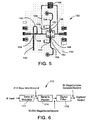
- FIG. 6 is a block diagram of an ADC 170 that can be used as the ADC 20 and 62 above.
- the ADC 170 includes a delta-sigma modulator 172 that receives the analog signal from the down-converter 18 and generates a representative stream of digital data at a very high clock rate, in a manner that will be discussed in detail below.
- the stream of digital data from the delta-sigma modulator 172 is sent to a serial-to-parallel converter 174 that de-multiplexes the delta samples to a word rate that is compatible with a CMOS processor.
- a digital filter 176 receives the digital data at the lower clock rate, and filters the signal to provide sixteen bit words suitable for the channelizer 22.
- FIG. 7 is a block diagram of the delta-sigma modulator 172.
- the delta-sigma modulator 172 includes a summation device 180 that receives the analog signal from the down-converter 18 and a negative feedback signal from the digital output of the modulator 172.
- the analog difference signal from the summation device 180 compensates for the error in the digital output of the modulator 172.
- the error is the difference between the input and the output of the modulator. By determining this error, the difference between the input and the output can be directed to zero or minimized for increased conversion accuracy.
- the difference signal from summation device 180 is applied to a filtering device 182 having a predetermined filter function that identifies the operational characteristics of the modulator 172.
- the filter function looks at the difference error signal and generates a voltage that amplifies the frequencies of interest in the error signal.
- the filtered error signal is applied to a sample and hold device 184 that samples the analog signal for a predetermined period of time, and provides a stable output voltage at the end of each hold period.
- the analog signal from the sample and hold device 184 is applied as an input to a comparator 186 that compares the analog signal to a threshold, here zero, and provides either a high or low logic output at each clock cycle f s .
- the high or low output represents a data bit.
- the output of the comparator 186 is a stream of digital data that is very fast, 2-4 gigabits/second.
- the sample and hold device 184 provides the ability to accurately track the output of the filtering device 182, and hold the last voltage tracked for some period of time, to allow the input to the comparator 186 to be more stable.
- An example of a sample and hold device that can be used for this purpose can be found in US Patent No. 4,370,572, titled Differential Sample-And-Hold Circuit.
- the digital output from the comparator 186 is used as a feedback signal in the delta-sigma modulator loop.
- the comparator 186 provides either a logical 1 state or a logical 0 state. In practice, the output is a high or low voltage representing the logical state. Energy coupling from the input of the comparator 186 to the output of the comparator 186 creates an uncertainty in the output voltage, where the output voltage may not be the exact output desired.
- a differential limiting amplifier 188 is provided to remove the small fluctuations in the output voltage of the comparator 186 that define the logical 1 or the logical 0. The output of the amplifier 188 does not have the fluctuations in voltage that the input voltage may have.
- the stable signal from the amplifier 188 is applied to a digital-to-analog converter (DAC) 190 that coverts the digital feedback signal to an analog signal to be subtracted from the analog input signal in the summation device 180.
- DAC digital-to-analog converter
- the DAC 190 is switched off during the time period that the comparator 186 is making its comparison to further reduce the effects of comparator output variations on the feedback signal.
- the modulator 172 may include more than one comparator 186, where the analog signal from the filtering device 182 is applied to all of the comparators in parallel, and each comparator compares the signal against a different threshold.
- Each comparator would include a separate differential amplifier and DAC, and all of the signals from the DACs would be added to the summation device 180.
- the sample and hold device 184 and the limiting amplifier 188 are not required for operation of the modulator 172. However, employing these components, either singly or in combination, allows the modulator 172 to operate more accurately at higher clock rates. Thus, the modulator 172 increases the accuracy of the analog-to-digital conversion for simultaneously processing multiple signals in the receivers 10 and 60, as discussed above.
- the differential limiting amplifier 188 can be provided in the comparator 186, or at other locations in the modulator 172.
- Figures 8(a)-8(c) show various versions of this embodiment.
- comparators 200, 202 and 204 are shown including a pre-amplifier 206 and a flip flop 208, including a master latch 210 and a slave latch 212.
- a differential limiting amplifier 214 is shown in different locations, including between the latches 210 and 212 (figure 8(a)); between the pre-amplifier 206 and the master latch 210 and between the latches 210 and 212 (figure 8(b)); and between the pre-amplifier 206 and the master gate 210, between the gates 210 and 212, and after the slave gate 212 (figure 8(c)).
- FIG. 9(a) shows a differential limiting amplifier 220 including differential pair transistors 222 and 224, and including a Schottky diode clamp 226 having Schottky diodes 232-238 connected between the collector terminals of the transistors 222 and 224.
- the Schottky diode clamp 226 consists of two sets of diode pairs. Each diode pair is connected in a series arrangement with the midpoint connection tied to a low impedance voltage source, for example, ground. The diode pairs are connected across the load resistors R L of the differential amplifier 220 in an anti-parallel fashion.
- Figure 9(b) shows a differential amplifier 228 including the transistors 222 and 224, and including a Schottky diode clamp 230 comprising Schottky diodes 240 and 242 connected between the collector terminals of the transistors 222 and 224.
- the amplifier 228 operates in the same manner as the amplifier 220.
- the filter 176 has a serial-to-parallel conversion module 250, a numerically controlled oscillator (NCO) 254, a digital mixer 256, and a plurality of filter and decimate stages 258, 260 and 262.
- the NCO 254 generates a frequency conversion signal based on a desired center frequency.
- the frequency conversion signal is equivalent to a sinewave having a 187.5MHz frequency.
- the digital mixer 256 has a first input code to the NCO 254 for mixing the individual carrier signals with the frequency conversion signal.
- the filter and decimate stages 258, 260, and 262 digitally filter each bit stream from the serial-to-parallel conversion module 250 based on a desired bandwidth.
- a first stage 258 is coupled to the serial-to-parallel conversion module 250.
- the output of the serial-to-parallel conversion module 250 is a low speed version of the output of converter 174. This enables the filter 176 to be implemented with a standard CMOS process.
- the first stage 258 is also coupled to a second input of the digital mixer 256, and essentially removes high frequency noise energy content from the digital data.
- the second stage 260 is coupled to an output of the digital mixer 256, and removes the remaining out-of-band noise and spurious energy content from the digital data.
- a third stage 262 is coupled to the second stage 260 to further remove out-of-bound energy content from the digital data. It is important to note that each stage results in less data, and therefore allows slower sample rates. This makes arithmetic processing easier and reduces overall system costs.
- each stage 258, 260 and 262 has a low pass filter and a decimation module.
- the first stage 258 includes low pass filter 252 and decimation module 264.
- the decimation module 264 is coupled to the low pass filter 252 for decimating the digital data by a factor.
- the decimation module 264 decimates by a factor of four. This means that three out of every four samples are removed, resulting in one-fourth of the incoming amount of data.
- the second stage 260 has a low pass filter 266 and a decimation module 268.
- the decimation module 268 decimates by eight.
- the third stage includes low pass filter 270 and decimation module 272, where the decimation module 272 decimates by two.
- the numerical coefficients of the low pass filters 252, 266 and 270 can be selected to provide the desired multi-channel bandwidth. It is also important to note that the center frequency of the NCO 254 is tunable to optimize the dynamic range of the A/D converter 176.
- Figures 11-14 show various embodiments of the channelizer 22 in greater detail.
- the channelizer 22 may be implemented as a Fast Fourier Transform (FFT), an array of quadrature mirror filters, a filter tree, or an array of digital sub-band tuners (DSBTs).
- FFT Fast Fourier Transform
- DSBTs digital sub-band tuners
- Figures 11 and 14 show that the preferred channelizer 22 has a plurality of DSBTs 274.
- Each DSBT 274 digitally filters individual carrier signals from a digital multi-carrier signal based on a programmable center frequency f c .
- the specifics of each DSBT 274 can be seen in Figure 10.
- each DSBT 274 also digitally filters the individual carrier signals based on a programmable bandwidth.
- all of the remaining in-band content from the A/D converter 20 is routed to the DSBTs 274.
- the DSBTs 274 can be allocated based on frequency or modulation format.
- the first DSBT 274a could digitally filter individual carrier data streams having a first modulation format (e.g., CDMA), and a second DSBT 274b could digitally filter individual carrier data streams having a second modulation format (e.g., GSM).
- An FFT could also be used to efficiently extract carriers and bands with a large number of regularly spaced carriers.
- the quadrature and tree filter structures provide the ability to efficiently implement channelizers with fixed channels of differing bandwidths.
- DSBTs permit programmable channel bandwith and center frequency use.
- each channelizer 22 may be implemented as logic elements on integrated circuits, or as programmable digital signal processors as required to achieve the desired bandwidths with the integrated circuit technology used.
- Figure 12 shows a first alternative embodiment, wherein a plurality of channelizers 22 are interconnected by a switch matrix 278.
- This permits arbitrary interconnection of the channelizers 22 to provide an optimum utilization of resources.
- the number of channelizers available, and the size of the switch matrix 278 are determined by the number and types of signals to be extracted. Channelizers of differing types, speeds, channel capacity, and accuracy can be included to optimize efficiency.
- An output formatter 280 arranges the extracted channels into one or more output data streams of one or more formats. Formats might be peripheral component interface (PCI) or other parallel interfaces. Formats may also be serial interfaces such as Ethernet, IEEE 1553, or IEEE 1394.
- PCI peripheral component interface
- Formats may also be serial interfaces such as Ethernet, IEEE 1553, or IEEE 1394.
- any interface used in computer applications or communications systems utilizing wire, optical fiber, optical, or wireless RF as media represent suitable formats.
- Buffer storage is included to permit the use of packet switched interface protocols or other protocols that do not provide a uniform flow of data.
- the output interface of the formatter 280 might serve as a gateway to other circuitry on a common assembly, to a backplane of a computer or other similar equipment, or to a network interface. Such a network interface would permit the distribution of each or all of the extracted signals to one or more destinations.
- FIG. 13 a second alternative approach to the channelizer 22 is shown.
- a plurality of channelizers 22 are cascaded through switch matrices 278 to permit sub-channelization.
- an initial channelizer 22a might select bands of specific formats, while subsequent channelizers 22b-22i would extract carriers within a band.
- each channelizer 22 can be individually tuned to any band for multi-carrier types or additional channels.
- FFT or quadrature/tree filter channelizer bandwidth and center frequency can be changed to accommodate different formats by varying the clock rate and input bandwidth from the preceding channelizer.
Abstract
Description
- This invention relates generally to a channelizer for a multi-carrier receiver and, more particularly, to a channelizer for a multi-carrier receiver that employs an array of digital sub-band tuners, FFTs, an array of quadrature mirror filters, or a filter tree.
- Wireless telecommunications systems, particularly cellular telephone communications systems, employ strategically placed base stations having transceivers that receive and transmit signals over a particular carrier frequency band to provide wireless communications between two parties. Depending on the particular area, each base station will include a certain number of receivers that receive the signals, and provide digital signal processing so that the signal is transmitted to the desired destination. Each receiver scans the frequency band of interest until it locks onto a signal in that band. The frequency band is usually at about 800MHz and higher with a bandwidth of 200KHz or more. An example with a bandwidth of 75MHz centered at about 1750MHz will be used in this description.
- A typical receiver for this application will include an antenna that receives the signals and a duplexer that limits the received signals to the desirable carrier frequency range in which the signals are transmitted. The frequency band limited signal received by the antenna is then applied to a low noise amplifier (LNA) where it is amplified to an amplitude suitable for subsequent processing. The band limited and amplified signal is then applied to a frequency down-converter that mixes the received signal with a local oscillator (LO) signal to generate a lower intermediate frequency (IF) signal that can be readily processed by the DSP devices. A bandpass filter (BPF) is typically employed in the frequency down-converter to limit the IF signal to the particular frequency band of the received signal. The filtered IF signal is then applied to an analog-to-digital converter (ADC) that converts the IF signal to a representative digital signal that is then processed by the DSP devices. The receiver may be designed to process signals for many protocols and standards, including time division multiple access (TDMA), code division multiple access (CDMA), enhanced data rate for global evolution (EDGE), Gaussian minimal shift keying (GMSK), etc., depending on the particular application.
- The known receiver described above for wireless telecommunications has only been capable of processing a single signal or a single channel at any given time. Thus, a separate receiver has been required in the base station for each separate signal being processed. Because certain base stations may have to receive and transmit many signals for multiple users simultaneously, these base stations must include enough receivers to satisfy this requirement, or service is lost. Because each receiver includes the various components that perform the signal receiving operation discussed above, high traffic base stations include a large amount of receiver hardware, and thus are costly. As cellular telephone communications increases, base stations will be required to provide more simultaneous access, or more base stations will be required, thus significantly increasing costs in these systems.
- What is needed is a wireless telecommunications system receiver that operates over a relatively wide bandwidth, and is capable of processing multiple signals in different frequency bands simultaneously. To process multiple signals simultaneously, the basic components, including the LNA, the frequency down-converter and the ADC, of the receiver need to be redesigned to provide the performance specifications and requirements necessary. Compared to the single channel receiver previously mentioned, the multiple channel receiver must continuously handle a much wider range of frequencies and larger range of power levels. In addition, the multiple channel receiver must be insensitive to potential cross-channel interference. It is therefore an object of the present invention to provide such a receiver having high performance components.
- In accordance with the teachings of the present invention, a channelizer for a multi-carrier receiver is disclosed that includes a plurality of digital sub-band tuners (DSBTs). Each DSBT digitally filters individual carrier data streams from a digital multi-carrier data stream based on a programmable center frequency. Each DSBT further digitally filters the individual carrier data streams based on a programmable bandwidth. The DSBTs can be allocated based on modulation format, center frequency, or both. The channelizer is therefore able to process narrow-band carrier data streams as well as wide-band carrier data streams. One embodiment of the channelizer has a plurality of sub-channelizers and a switch matrix. The sub-channelizers filter sub-sets of carrier data streams from a multi-carrier data stream. The switch matrix is coupled to the sub-channelizers and routes the individual data streams to the sub-channelizers in a desired configuration.
- Additional objects, advantages and features of the present invention will become apparent from the following description and appended claims, taken in conjunction with the accompanying drawings.
-
- Figure 1 is a block diagram of a receiver for a telecommunications system capable of processing multiple signals simultaneously, and employing a single frequency down-conversion process. according to an embodiment of the present invention;
- Figure 2 is a block diagram of a receiver for a wireless telecommunications system capable of processing multiple signals simultaneously, and employing a double frequency down-conversion process, according to another embodiment of the present invention;
- Figure 3 is a schematic block diagram of a balanced low noise amplifier network that can be used in the receivers shown in Figures 1 and 2, according to the invention;
- Figure 4 is a schematic diagram of an MMIC amplifier used in the balanced amplifier network shown in Figure 3, according to the invention;
- Figure 5 is a component layout diagram of the amplifier shown in Figure 4;
- Figure 6 is a block diagram of a delta-sigma analog-to-digital converter that can be used in the receivers shown Figures 1 and 2, according to the invention;
- Figure 7 is a detailed block diagram of the delta-sigma modulator used in the analog-to-digital converter shown in Figure 6;
- Figures 8(a)-8(c) are block diagrams showing different embodiments of a comparator that can be employed in the delta-sigma modulator shown in Figure 7, and including a limiting amplifier, according to the invention;
- Figures 9(a)-9(b) are schematic diagrams of various differential limiting amplifiers than can be used in the delta-sigma modulators shown in Figures 7-8(c), according to the invention;
- Figure 10 is a block diagram of the digital filter used in the analog-to-digital converter shown in Figure 6, according to the invention;
- Figure 11 is a block diagram of a digital channelizer that can be used in both the receivers shown in Figures 1 and 2, according to the invention;
- Figure 12 is a block diagram of a reconfigurable channelizer, according to another embodiment of the present invention;
- Figure 13 is a block diagram of a cascaded channelizer, according to another embodiment of the present invention; and
- Figure 14 is a block diagram of a channelizer including an array of sub-band tuners, according to another embodiment of the present invention.
- The following discussion of the preferred embodiments directed to a receiver, and its components, for a wireless telecommunications system that is capable of processing multiple cellular signals simultaneously is merely exemplary in nature, and is in no way intended to limit the invention or its applications or uses. Particularly, the receiver disclosed herein may be applicable for other wireless communication systems besides cellular communications systems, and the particular components disclosed herein may be applicable for other systems and applications.
- Figure 1 is a block diagram of a
receiver 10 for a wireless telecommunications system, such as cellular communications system, according to an embodiment of the present invention. Thereceiver 10 has particular application for a cellular base station, and has an advantage over those receivers known in the art because it is capable of processing multiple received signals simultaneously at any particular time, as opposed to a single received signal. As will be discussed in detail below, the various components and devices in thereceiver 10 are designed to process signals over a relatively wide frequency band so that multiple signals transmitted at different carrier frequencies can be processed simultaneously. Thus, the receiver hardware in the base station can be limited accordingly. - Transmitted signals are received by an
antenna 12 in thereceiver 10. The signals received by theantenna 12 are applied to aduplexer 14 that only passes the signals in a particular receive frequency band of interest. The function and operation of theduplexer 14 is well understood to those skilled in the art. Different frequency bands may be used by different telecommunications systems. In one example, the frequency band of interest has a bandwidth of about 75MHz centered at 1750MHz. - According to an embodiment of the present invention, the
receiver 10 includes anLNA 16, a frequency down-converter 18, anADC 20 and adigital channelizer 22 that process the received signals over the wideband. The frequency down-converter 18 includes anLO 26, amixer 28, anamplifier 30, aBPF 32, anattenuator 34 and atransformer 36. TheLO 26 includes an LOfrequency reference source 40, asynthesizer 42, first andsecond amplifiers frequency multiplier 48. Each of theLNA 16, the frequency down-converter 18, theADC 20 and thedigital channelizer 22 are specialized components that operate in connection with each other to pass a relatively wide frequency band, without degrading receiver performance, so that multiple signals can be simultaneously processed by thereceiver 10. Specifics of thespecialized LNA 16, theADC 20 and thechannelizer 22 will be discussed below. - The band limited signal from the
duplexer 14 is applied to theLNA 16 to amplify the low power signal from theantenna 12 to a desired amplitude. In one embodiment, theLNA 16 is optimized for a particular frequency band, for example, 1722.5-1772.5 MHz. The amplified signal from theLNA 16 is applied to themixer 28 along with an LO signal from theamplifier 44 to down-convert the received signal to a lower frequency. The LO signal is generated by thereference source 40 and is tuned by thesynthesizer 42 to a particular center frequency. The output of themixer 28 is an IF signal suitable for subsequent digital signal processing. - The IF signal is bandpass limited by the
BPF 32 to a particular frequency band. In one embodiment, thesynthesizer 42 tunes the reference frequency between 1497.5MHz - 1622.5MHz to generate the IF signal from themixer 28 at a center frequency of 187.5MHz, and theBPF 32 passes signals over a 25MHz frequency band centered at 187.5MHz. These frequencies are identified by way of non-limiting examples in that other systems may employ other frequency bands within the scope of the present invention. The combination of themixer 28 and theBPF 32 provide the desired frequency control of the IF signal during the down-conversion step. The other components in the down-converter 18, particularly theamplifier 30, theattenuator 34 and thetransformer 36, provide the desired amplitude adjustment of the IF signal. Thetransformer 36 converts the IF signal into a form suitable for theADC 20, as is well known in the art. - The
ADC 20 provides the necessary speed and device performance to convert the IF signal at the wideband frequency range into a digital signal in a high performance manner. TheADC 20 must simultaneously process both weak and strong signals. In one embodiment, theADC 20 employs delta-sigma processing, as described in detail later in this description. To allow theADC 20 to operate in this manner, the LO signal from thesynthesizer 42 is used as a timing signal. The frequency of the LO signal is doubled by themultiplier 48, amplified by theamplifier 46, and then applied to theADC 20. By providing this input to theADC 20, changes in the synthesizer output do not induce distortions into the analog-to-digital conversion. In other words, the signal from theamplifier 46 to theADC 20 acts as a clock input at a clock rate determined by thesynthesizer 42 for more optimal device performance. - The digitally converted signal from the
ADC 20 is then applied to thedigital channelizer 22 that separates all of the received signals across the wide bandwidth into the separate signals for subsequent digital signal processing. In other words, all of the adjacent frequency bands in the IF signal passed by theBPF 32 are converted to a digital signal by theADC 20, and then separated into their respective frequency bands by thechannelizer 22. The separated signals can then be processed in the normal manner by subsequent DSP devices (not shown). - Because the performance and operation of the
LNA 16, the frequency down-converter 18, and theADC 20 are optimized for the wide frequency band without inducing distortions to the received signals, thedigital channelizer 22 is able to readily separate the signals in the digital domain without adding distortion. In this example, thedigital channelizer 22 provides four separate signals. However, this is by way of a non-limiting example, in that other applications may include two outputs, eight outputs, sixteen outputs, etc., within the scope of the present invention. - The cascaded combination of LNA, mixer, filters, and attenuators must maintain high sensitivity and low distortion for a wide range of frequencies and channel power levels. Choice of component parameter values (gain, noise level, linearity) is critical for the multiple channel receiver. Too much gain or insufficient linearity (characterized by input (IIP) or output (OIP) intercept power levels) jeopardizes channel intermodulation. Too little gain or too large component noise threatens receiver sensitivity.
- Table I below shows specific components for the
receiver 10 and component performance, and Table II gives overall performance of thereceiver 10.TABLE I Stage Component Gain (dB. typ) NF(db. typ) IIP (dbm. typ) OIP (dBm, typ) LNA A1-TRW 23.0 0.35 11.0 34.0 Mix-1 HMJ7 -8.5 10.50 39.0 30.5 Amp-1 AH3 14.0 3.00 26.0 40.0 Flt-1 MLP_265_3_RA -3.0 3.00 >103.0 >100.0 Attn-1 Attn-3 -3.0 3.00 >103.0 >100.0 ADC DS-ADC N/A 12.40 N/A N/A TABLE II Receiver Performer Condition Min Typ Max Gain (dB) 20.8 22.5 23.4 NF (dBm) 0.81 1.03 1.44 IIP (dBm) 6.8 7.4 8.5 OIP (dBm) 28.7 29.9 30.8 - Figure 2 is a block diagram of a
receiver 60, similar to thereceiver 10 described above, where like components are identified by the same reference numeral and operate in the same manner. The down-converter 18 in thereceiver 10 provided a single step down-conversion from the high carrier frequency received by theantenna 12 to the IF signal. In this embodiment, theADC 20 was complex to provide the necessary digital conversion at the higher IF (187.5MHz). However, this embodiment provided less receiver hardware, i.e., a single mixer, a single BPF, etc. For thereceiver 60, a double frequency down-conversion process is performed by the down-converter 18 to reduce the frequency of the IF signal to a lower frequency so that anADC 62 can be employed that has a lower center frequency. - In the
receiver 60, thesynthesizer 42 is tuned so that the IF signal from themixer 28 is about 228MHz, and thus may be different than the IF signal from themixer 28 in thereceiver 10. Asecond mixer 64 is provided after theBPF 32 to further reduce the frequency of the IF signal to about (28MHz). Asynthesizer 66 is provided to tune themixer 64, and anamplifier 68 is provided to amplify the signal applied to themixer 64. In this embodiment, the baseband signal is amplified by anamplifier 70 and is passed through a low pass filter (LPF) 72. Thefrequency multiplier 48 has been replaced with afrequency divider 74 that divides the signal from thesynthesizer 66 to provide the clock signal to theADC 62 through theamplifier 46. Thedivider 74 is used because theADC 62 clock has to follow the lower IF. A double frequency down-conversion process is required to center the signal band at 28MHz with minimal interference from conversion products. - Table III below gives components for the
receiver 60 and component performance, where theADC 62 is a delta-sigma ADC, and Table IV gives overall receiver performance. Table V below gives components for thereceiver 60 and component performance, where theADC 62 is a commercially available ADC, and Table VI gives overall receiver performance.TABLE III Stage Component Gain (dB. typ NF (db, typ) IIP (dbm, typ) OIP (dBm, typ) LNA A1-TRW 23.0 0.35 11.0 34.0 Mix-1 HMJ7 -8.5 10.50 39.0 30.5 Amp-1 AH3 14.0 3.00 26.0 40.0 Fit-1 BPFxx -3.0 3.00 >103.0 >100.0 Mix-2 HMJ5 -6.3 8.30 38.0 31.7 Amp-2 ARJ109 10.8 4.50 33.2 44.0 Attn-1 Attn-7 -7.0 7.00 >107.0 >100.0 ADC DS-ADC N/A 12.40 N/A N/A TABLE IV Receiver Performer Condition Min Typ Max Gain (dB) 20.9 23.0 24.4 NF (dB) 0.88 1.13 1.61 IIP (dB) 4.9 5.5 6.7 OIP (dBm) 26.8 28.5 29.7 TABLE V Stage Component Gain (dB. typ NF (db. typ) IIP (dbm. typ) OIP (dBm. typ) LNA A1-TRW 23.0 0.35 11.0 34.0 Mix-1 HMJ7 -8.5 10.50 39.0 30.5 Amp-1 AH3 14.0 3.00 26.0 40.0 Flt-1 BPFxx -3.0 3.00 >103.0 >100.0 Mix-2 HMJ5 -6.3 8.30 38.0 31.7 Amp-2 ARJ109 10.8 4.50 33.2 44.0 Attn-2 Attn-2 -2.0 2.00 >102.0 >100.0 ADC AD6644 N/A 20.30 N/A N/A TABLE VI Receiver Performer Condition Min Typ Max Gain (dB) 25.9 28.0 29.4 NF (dB) 1.10 1.39 1.99 IIP (dBm) 2.8 3.6 5.0 OIP (dBm) 30.4 31.6 32.3 - Figure 3 is a schematic block diagram of a
balanced amplifier network 80, according to an embodiment of the present invention, that can be used as theLNA 16 discussed above. It is stressed, however, that thenetwork 80 has application for other systems. The basic design of thenetwork 80 is known in the art, and therefore only a cursory discussion of the operation of thenetwork 80 will be given below. Thenetwork 80 includes afirst amplifier 82 positioned in afirst amplification path 84 of thenetwork 80, and asecond amplifier 86 positioned in asecond amplification path 88 of thenetwork 80. A schematic diagram of theamplifier 82 is shown in figure 4, with the understanding that theamplifier 86 is the same. As will be discussed below, theamplifier 82 includes a field effect transistor (FET) 90 and a plurality of oscillation stabilization components that are monolithically integrated in a monolithic microwave integrated circuit (MMIC) on a thin substrate, according to the invention. - The
network 80 includes an input 90-degree hybrid coupler 110 and an output 90-degree hybrid coupler 112. The signals from theduplexer 14 are applied to theinput terminal 92 of thecoupler 110 so that the 0-phase of the input signal is provided on thefirst path 84 and the 90-degree phase of the input signal is provided on thesecond path 88. A first inputimpedance matching network 114 is provided on thefirst path 84 between theinput coupler 110 and theamplifier 82, and a second inputimpedance matching network 116 is provided on thesecond path 88 between theinput coupler 110 and theamplifier 86. Likewise, a first outputimpedance matching network 118 is provided on thefirst path 84 between theamplifier 82 and theoutput coupler 112, and a second outputimpedance matching network 120 is provided on thesecond path 88 between theamplifier 86 and theoutput coupler 112. - The
impedance matching networks amplifiers FET 90. The phase difference of the signals on the first andsecond paths input terminal 92. Theoutput matching networks FET 90. Theoutput coupler 112 combines the output power for both of theamplifiers output terminal 122. - By providing a short gate length, the
FET 90 is a high frequency amplifier capable of amplifying signals up 80-100 GHz. Because theFET 90 is able to amplify signals at very high frequencies with low noise and good output power, it is desirable for the wide bandwidth, low noise application for thereceivers network 80 is designed to amplify signals at about 2GHZ for the cellular transmission application. Thus, there is a concern that theFET 90 may oscillate at the higher frequencies (above 5GHZ), which will degrade device performance. Small changes in impedance at the input and output of theFET 90 cause high frequency instability in theFET 90, that creates the high frequency oscillations. To prevent the high frequency oscillations, it is necessary to be concerned about the connections around theFET 90, and provide stabilization components connected to theFET 90 on the same substrate. - The
amplifier 82 includes aninput port 94 and anoutput port 96. A large resistor R3 and a capacitor C1 are connected between the gate and drain terminals of theFET 90. The resistor R3 and the capacitor C1 reduce gain at low frequencies, and help prevent the amplifier gain from getting high at low frequencies. Further, an inductor L1 and a resistor R2 are connected in parallel with each other and between theinput port 94 and the gate terminal of theFET 90. As the reactance of the circuit goes up as the frequency goes up, the resistor R2 becomes a high loss device that acts to limit the gain of theFET 90 at the high frequencies. The inductor L1 is very low inductance, so it only works at high frequencies and will pass signals at low frequency. Also, a resistor R1 and an open-endedtransmission line 98 are connected in series with each other and to theinput port 94. As the frequency increases, thetransmission line 98 becomes low impedance, so that current can flow through the resistor R1 providing a shunt load on theinput port 94 at high frequencies to reduce the gain of theFET 90 at these frequencies. An inductor L2 is connected to the source terminal of theFET 90, and is used to improve the input match for low noise amplifiers. A resistor R4 and an openend transmission line 100 are connected to the source terminal, and operate in the same manner as the resistor R1 and thetransmission line 98 for the source terminal. At low frequencies, the resistor R4 acts as an open circuit. As the frequency increases, thetransmission line 100 becomes low impedance, so that current will flow through the resistor R4, providing a reduction in the Q of L2. - The particular circuit configuration of the stabilization components discussed above is shown by way of a non-limiting example in that other circuit configurations can be used to provide the desired stabilization at high frequency, as would be appreciated by those skilled in the art. One of ordinary skill in the art would understand the operation of the stabilizing components discussed herein, and would know what component values would be needed for proper device operation.
- As discussed above, the oscillation stabilization components prevent the amplifier from amplifying above a certain frequency, and thus oscillations do not occur at these frequencies. A problem exists in this approach for
amplifier 80. The short wavelengths at higher frequencies cause the stabilization components implemented on a thick substrate to become unpredictable. As the frequency gets higher, the substrate thickness must get smaller for the stabilization components to have predictable operation in achieving the desired stabilization. As the thickness of the substrate increases, the components behave in a less predictable manner. However, for thin substrates, the transmission lines need to be narrow for proper device impedance matching. But, narrow transmission lines have a high resistance, which significantly increases loss. Therefore, it is undesirable to include all of the components of theamplifier network 80 on a thin substrate because the losses would be unacceptable. - According to the present invention, the
FET 90 and the stabilization components R1, R2, R3, R4, C1, L1, L2, and thetransmission lines network 80 are integrated on a thick substrate as a microwave integrated circuit (MIC). Because theMMIC amplifiers amplifiers network 80 is about 20-50 mils. The substrate material can be GaAs, InP, or any other suitable semiconductor material. - Figure 5 is a circuit plan view of an
amplifier 130, representing theamplifier 82, to show the monolithically integrated location of the components discussed above on amonolithic substrate 132. In this embodiment, thesubstrate 132 is GaAs. Particularly, the resistor R1 is shown atlocation 134, the resistor R2 is shown atlocation 136, the resistor R3 is shown atlocation 138, the inductor L1 is shown atlocation 140, thetransmission line 98 is shown atlocation 142, and the capacitor C1 is shown atlocation 144. In this design, theFET 90 is twoFETs transmission line 100 includestransmission lines inductors resistors - Figure 6 is a block diagram of an
ADC 170 that can be used as theADC ADC 170 includes a delta-sigma modulator 172 that receives the analog signal from the down-converter 18 and generates a representative stream of digital data at a very high clock rate, in a manner that will be discussed in detail below. The stream of digital data from the delta-sigma modulator 172 is sent to a serial-to-parallel converter 174 that de-multiplexes the delta samples to a word rate that is compatible with a CMOS processor. Adigital filter 176 receives the digital data at the lower clock rate, and filters the signal to provide sixteen bit words suitable for thechannelizer 22. - Figure 7 is a block diagram of the delta-
sigma modulator 172. The delta-sigma modulator 172 includes asummation device 180 that receives the analog signal from the down-converter 18 and a negative feedback signal from the digital output of themodulator 172. The analog difference signal from thesummation device 180 compensates for the error in the digital output of themodulator 172. The error is the difference between the input and the output of the modulator. By determining this error, the difference between the input and the output can be directed to zero or minimized for increased conversion accuracy. - The difference signal from
summation device 180 is applied to afiltering device 182 having a predetermined filter function that identifies the operational characteristics of themodulator 172. The filter function looks at the difference error signal and generates a voltage that amplifies the frequencies of interest in the error signal. The filtered error signal is applied to a sample and holddevice 184 that samples the analog signal for a predetermined period of time, and provides a stable output voltage at the end of each hold period. The analog signal from the sample and holddevice 184 is applied as an input to acomparator 186 that compares the analog signal to a threshold, here zero, and provides either a high or low logic output at each clock cycle fs. The high or low output represents a data bit. The output of thecomparator 186 is a stream of digital data that is very fast, 2-4 gigabits/second. - One of the problems with using the
comparator 186 in this manner is the inherent inability of thecomparator 186 to accurately convert the analog signal to a digital signal because the analog signal is rapidly changing. In other words, the rapidly changing analog signal limits the ability of thecomparator 186 to accurately determine the proper digital output. According to the invention, the sample and holddevice 184 provides the ability to accurately track the output of thefiltering device 182, and hold the last voltage tracked for some period of time, to allow the input to thecomparator 186 to be more stable. An example of a sample and hold device that can be used for this purpose can be found in US Patent No. 4,370,572, titled Differential Sample-And-Hold Circuit. - The digital output from the
comparator 186 is used as a feedback signal in the delta-sigma modulator loop. Thecomparator 186 provides either a logical 1 state or a logical 0 state. In practice, the output is a high or low voltage representing the logical state. Energy coupling from the input of thecomparator 186 to the output of thecomparator 186 creates an uncertainty in the output voltage, where the output voltage may not be the exact output desired. To correct for this uncertainty, according to the invention, a differential limitingamplifier 188 is provided to remove the small fluctuations in the output voltage of thecomparator 186 that define the logical 1 or the logical 0. The output of theamplifier 188 does not have the fluctuations in voltage that the input voltage may have. - The stable signal from the
amplifier 188 is applied to a digital-to-analog converter (DAC) 190 that coverts the digital feedback signal to an analog signal to be subtracted from the analog input signal in thesummation device 180. In one embodiment, theDAC 190 is switched off during the time period that thecomparator 186 is making its comparison to further reduce the effects of comparator output variations on the feedback signal. - In an alternate embodiment, the
modulator 172 may include more than onecomparator 186, where the analog signal from thefiltering device 182 is applied to all of the comparators in parallel, and each comparator compares the signal against a different threshold. Each comparator would include a separate differential amplifier and DAC, and all of the signals from the DACs would be added to thesummation device 180. - The sample and hold
device 184 and the limitingamplifier 188 are not required for operation of themodulator 172. However, employing these components, either singly or in combination, allows themodulator 172 to operate more accurately at higher clock rates. Thus, themodulator 172 increases the accuracy of the analog-to-digital conversion for simultaneously processing multiple signals in thereceivers - The
modulator 172 discussed above included the differential limitingamplifier 188 in the feedback path. In alternate embodiments, the differential limitingamplifier 188 can be provided in thecomparator 186, or at other locations in themodulator 172. Figures 8(a)-8(c) show various versions of this embodiment. In these figures,comparators pre-amplifier 206 and aflip flop 208, including amaster latch 210 and aslave latch 212. A differential limitingamplifier 214 is shown in different locations, including between thelatches 210 and 212 (figure 8(a)); between the pre-amplifier 206 and themaster latch 210 and between thelatches 210 and 212 (figure 8(b)); and between the pre-amplifier 206 and themaster gate 210, between thegates - Schematic diagrams of different embodiments of a differential limiting amplifier suitable for the purposes discussed herein are shown in figures 9(a) and 9(b). Figure 9(a) shows a differential limiting
amplifier 220 includingdifferential pair transistors Schottky diode clamp 226 having Schottky diodes 232-238 connected between the collector terminals of thetransistors Schottky diode clamp 226 consists of two sets of diode pairs. Each diode pair is connected in a series arrangement with the midpoint connection tied to a low impedance voltage source, for example, ground. The diode pairs are connected across the load resistors RL of thedifferential amplifier 220 in an anti-parallel fashion. This arrangement insures that when the diodes 232-238 turn on, the voltage at each differential output clamps in a symmetrical fashion, i.e., one diode forward drop above the midpoint voltage and one diode forward drop below the midpoint voltage. Thus, the output nodes of theamplifier 220 are held at a low impedance. When the input voltage of the limitingamplifier 220 reverses polarity, the alternate pair of diodes turn on, again maintaining symmetry and low impedance. - Figure 9(b) shows a
differential amplifier 228 including thetransistors Schottky diode clamp 230 comprisingSchottky diodes transistors amplifier 228 operates in the same manner as theamplifier 220. - Turning now to Figure 10, the
digital filter 176 will be described in greater detail. Generally, thefilter 176 has a serial-to-parallel conversion module 250, a numerically controlled oscillator (NCO) 254, adigital mixer 256, and a plurality of filter and decimatestages NCO 254 generates a frequency conversion signal based on a desired center frequency. In the illustrated example, the frequency conversion signal is equivalent to a sinewave having a 187.5MHz frequency. Thedigital mixer 256 has a first input code to theNCO 254 for mixing the individual carrier signals with the frequency conversion signal. The filter and decimatestages parallel conversion module 250 based on a desired bandwidth. - Specifically, it can be seen that a
first stage 258 is coupled to the serial-to-parallel conversion module 250. The output of the serial-to-parallel conversion module 250 is a low speed version of the output ofconverter 174. This enables thefilter 176 to be implemented with a standard CMOS process. Thefirst stage 258 is also coupled to a second input of thedigital mixer 256, and essentially removes high frequency noise energy content from the digital data. Thesecond stage 260 is coupled to an output of thedigital mixer 256, and removes the remaining out-of-band noise and spurious energy content from the digital data. In one embodiment, athird stage 262 is coupled to thesecond stage 260 to further remove out-of-bound energy content from the digital data. It is important to note that each stage results in less data, and therefore allows slower sample rates. This makes arithmetic processing easier and reduces overall system costs. - Generally, each
stage first stage 258 includeslow pass filter 252 anddecimation module 264. Thedecimation module 264 is coupled to thelow pass filter 252 for decimating the digital data by a factor. Thedecimation module 264 decimates by a factor of four. This means that three out of every four samples are removed, resulting in one-fourth of the incoming amount of data. Thesecond stage 260 has alow pass filter 266 and adecimation module 268. Thedecimation module 268 decimates by eight. Similarly, the third stage includeslow pass filter 270 anddecimation module 272, where thedecimation module 272 decimates by two. In each stage, increase in word length accompanies the decimation in order to preserve the full in-band information content. The numerical coefficients of the low pass filters 252, 266 and 270 can be selected to provide the desired multi-channel bandwidth. It is also important to note that the center frequency of theNCO 254 is tunable to optimize the dynamic range of the A/D converter 176. - Figures 11-14 show various embodiments of the
channelizer 22 in greater detail. Thechannelizer 22 may be implemented as a Fast Fourier Transform (FFT), an array of quadrature mirror filters, a filter tree, or an array of digital sub-band tuners (DSBTs). Specifically, Figures 11 and 14 show that thepreferred channelizer 22 has a plurality of DSBTs 274. Each DSBT 274 digitally filters individual carrier signals from a digital multi-carrier signal based on a programmable center frequency fc. The specifics of each DSBT 274 can be seen in Figure 10. With continuing reference to Figure 14, it will be appreciated that each DSBT 274 also digitally filters the individual carrier signals based on a programmable bandwidth. Thus, all of the remaining in-band content from the A/D converter 20 is routed to the DSBTs 274. - The DSBTs 274 can be allocated based on frequency or modulation format. For example, the
first DSBT 274a could digitally filter individual carrier data streams having a first modulation format (e.g., CDMA), and asecond DSBT 274b could digitally filter individual carrier data streams having a second modulation format (e.g., GSM). An FFT could also be used to efficiently extract carriers and bands with a large number of regularly spaced carriers. The quadrature and tree filter structures provide the ability to efficiently implement channelizers with fixed channels of differing bandwidths. As already discussed, DSBTs permit programmable channel bandwith and center frequency use. It will further be appreciated that each channelizer 22 may be implemented as logic elements on integrated circuits, or as programmable digital signal processors as required to achieve the desired bandwidths with the integrated circuit technology used. - Figure 12 shows a first alternative embodiment, wherein a plurality of
channelizers 22 are interconnected by aswitch matrix 278. This permits arbitrary interconnection of thechannelizers 22 to provide an optimum utilization of resources. The number of channelizers available, and the size of theswitch matrix 278 are determined by the number and types of signals to be extracted. Channelizers of differing types, speeds, channel capacity, and accuracy can be included to optimize efficiency. Anoutput formatter 280 arranges the extracted channels into one or more output data streams of one or more formats. Formats might be peripheral component interface (PCI) or other parallel interfaces. Formats may also be serial interfaces such as Ethernet, IEEE 1553, or IEEE 1394. Essentially, any interface used in computer applications or communications systems utilizing wire, optical fiber, optical, or wireless RF as media represent suitable formats. Buffer storage is included to permit the use of packet switched interface protocols or other protocols that do not provide a uniform flow of data. Furthermore, the output interface of theformatter 280 might serve as a gateway to other circuitry on a common assembly, to a backplane of a computer or other similar equipment, or to a network interface. Such a network interface would permit the distribution of each or all of the extracted signals to one or more destinations. - Turning now to Figure 13, a second alternative approach to the
channelizer 22 is shown. In this embodiment, a plurality ofchannelizers 22 are cascaded throughswitch matrices 278 to permit sub-channelization. Thus, aninitial channelizer 22a might select bands of specific formats, whilesubsequent channelizers 22b-22i would extract carriers within a band. As already discussed, eachchannelizer 22 can be individually tuned to any band for multi-carrier types or additional channels. Furthermore, FFT or quadrature/tree filter channelizer bandwidth and center frequency can be changed to accommodate different formats by varying the clock rate and input bandwidth from the preceding channelizer. - The foregoing discussion discloses and describes merely exemplary embodiments of the present invention. One skilled in the art will readily recognize from such discussion and from the accompanying drawings and claims, that various changes, modifications and variations can be made therein without departing from the spirit and scope the invention as defined in the following claims.
Claims (10)
- A channelizer for a multi-carrier receiver, the channelizer comprising:a plurality of digital sub-band tuners (DSBTs);each DSBT digitally filtering individual carrier data streams from a digital multi-carrier data stream based on a programmable center frequency; andeach DSBT further digitally filtering the individual carrier data streams based on a programmable bandwidth.
- The channelizer of Claim 1 wherein the plurality of DSBTs include:a first DSBT for digitally filtering individual carrier data streams having a first modulation format; anda second DSBT for digitally filtering individual carrier data streams having a second modulation format.
- The channelizer of Claim 2 wherein the first modulation format is a code division multiple access (CDMA) format.
- The channelizer of Claim 2 wherein the second modulation format is a GSM format.
- The channelizer of Claim 1 wherein each DSBT includes:a numerically controlled oscillator for generating a frequency conversion data stream based on the programmable center frequency;a digital mixer having a first input coupled to the oscillator for mixing the individual carrier data streams with the frequency conversion data stream; anda plurality of filter and decimate stages for digitally filtering the individual carrier data streams based on the programmable bandwidth.
- The channelizer of Claim 5 wherein the plurality of filter and decimate stages includes:a first stage coupled to a serial to parallel conversion module and a second input of the digital mixer, the first stage removing a first energy content from the individual carrier data streams;a second stage coupled to an output of the digital mixer, the second stage removing a second energy content from the individual carrier data streams; anda third stage coupled to the second stage, the third stage removing a third energy content from the individual carrier data streams.
- The channelizer of Claim 6 wherein each stage includes:a low pass filter; anda decimation module coupled to the low pass filter for decimating the individual carrier data streams by a number of reduction bits.
- A channelizer for a multi-carrier receiver, the channelizer comprising:a plurality of sub-channelizers for filtering individual carrier data streams from a multi-carrier data stream; anda switch matrix coupled to the sub-channelizer, said switch matrix routing the multi-carrier data stream and the individual data streams to the sub-channelizers in a desired configuration.
- The channelizer of Claim 8 wherein the sub-channelizers are cascaded.
- The channelizer of Claim 8 wherein one or more of the sub-channelizers include a Fast Fourier Transform (FFT) circuit.
Applications Claiming Priority (2)
| Application Number | Priority Date | Filing Date | Title |
|---|---|---|---|
| US605250 | 2000-06-28 | ||
| US09/605,250 US6760342B1 (en) | 2000-06-28 | 2000-06-28 | Channelizer for a multi-carrier receiver |
Publications (3)
| Publication Number | Publication Date |
|---|---|
| EP1168646A2 true EP1168646A2 (en) | 2002-01-02 |
| EP1168646A3 EP1168646A3 (en) | 2006-09-20 |
| EP1168646B1 EP1168646B1 (en) | 2008-04-02 |
Family
ID=24422868
Family Applications (1)
| Application Number | Title | Priority Date | Filing Date |
|---|---|---|---|
| EP01113540A Expired - Lifetime EP1168646B1 (en) | 2000-06-28 | 2001-06-12 | A channelizer for a multi-carrier receiver |
Country Status (4)
| Country | Link |
|---|---|
| US (1) | US6760342B1 (en) |
| EP (1) | EP1168646B1 (en) |
| JP (1) | JP2002057593A (en) |
| DE (1) | DE60133435T2 (en) |
Cited By (5)
| Publication number | Priority date | Publication date | Assignee | Title |
|---|---|---|---|---|
| WO2004006434A1 (en) * | 2002-07-04 | 2004-01-15 | R. F. Engines Limited | Frequency content separation using complex frequency shifting converters |
| WO2005015760A1 (en) * | 2003-07-10 | 2005-02-17 | Honeywell International | Radio receiver for aviation communications and navigation |
| US8019338B2 (en) | 2008-05-29 | 2011-09-13 | Honeywell International Inc. | Reconfigurable aircraft communications system with integrated avionics communication router and audio management functions |
| US8081933B2 (en) | 2007-07-13 | 2011-12-20 | Honeywell International Inc. | Reconfigurable aircraft radio communications system |
| US8711993B2 (en) | 2010-12-10 | 2014-04-29 | Honeywell International Inc. | Wideband multi-channel receiver with fixed-frequency notch filter for interference rejection |
Families Citing this family (24)
| Publication number | Priority date | Publication date | Assignee | Title |
|---|---|---|---|---|
| US20090031419A1 (en) | 2001-05-24 | 2009-01-29 | Indra Laksono | Multimedia system and server and methods for use therewith |
| US8291457B2 (en) | 2001-05-24 | 2012-10-16 | Vixs Systems, Inc. | Channel selection in a multimedia system |
| US7079828B1 (en) * | 2002-10-25 | 2006-07-18 | Edgewater Computer Systems, Inc. | Method and apparatus for side-lobe cancellation in wideband radio systems |
| US7424039B2 (en) * | 2003-03-28 | 2008-09-09 | Nortel Networks Limited | Method and apparatus for processing multiple common frequency signals through a single cable |
| US7782827B2 (en) * | 2003-03-28 | 2010-08-24 | Nortel Networks Limited | Method and apparatus for processing multiple common frequency signals through a single cable using circulators |
| US7729726B2 (en) * | 2004-03-26 | 2010-06-01 | Nortel Networks Limited | Feeder cable reduction |
| US8135086B1 (en) | 2004-08-09 | 2012-03-13 | Rockstar Bidco, LP | Cable reduction |
| MX2007002265A (en) | 2004-08-26 | 2007-04-20 | Interdigital Tech Corp | Method and apparatus for processing multiple wireless communication services. |
| US9602144B2 (en) * | 2004-08-26 | 2017-03-21 | Interdigital Technology Corporation | Method and apparatus for processing multiple wireless communication services |
| US20060045126A1 (en) * | 2004-08-30 | 2006-03-02 | Interdigital Technology Corporation | Method and apparatus for adaptively selecting sampling frequency for analog-to-digital conversion |
| US8452333B2 (en) * | 2005-12-12 | 2013-05-28 | Apple Inc. | Feeder cable reduction |
| US8260144B2 (en) | 2008-03-12 | 2012-09-04 | Hypres Inc. | Digital radio frequency tranceiver system and method |
| US8892225B2 (en) * | 2009-04-17 | 2014-11-18 | Maxlinear, Inc. | Wideband personal-radio recorder |
| US8526898B2 (en) | 2009-04-17 | 2013-09-03 | Maxlinear, Inc. | Wideband tuner architecture |
| US8548034B2 (en) * | 2010-02-08 | 2013-10-01 | Maxlinear, Inc. | Methods and apparatus for intelligent power reduction in communications systems |
| DE102012107877B4 (en) * | 2012-08-27 | 2016-01-07 | Epcos Ag | duplexer |
| CA2884728C (en) | 2012-09-14 | 2016-09-13 | Mitsubishi Electric Corporation | Relay device, satellite relay device, and satellite relay method |
| US20140163940A1 (en) * | 2012-12-11 | 2014-06-12 | David E. Erisman | Method and system for modeling rf emissions occurring in a radio frequency band |
| US9831898B2 (en) * | 2013-03-13 | 2017-11-28 | Analog Devices Global | Radio frequency transmitter noise cancellation |
| US10027026B2 (en) | 2014-09-18 | 2018-07-17 | Raytheon Company | Programmable beamforming system including element-level analog channelizer |
| US9912358B2 (en) | 2015-03-20 | 2018-03-06 | Analog Devices Global | Method of and apparatus for transmit noise reduction at a receiver |
| US10230407B2 (en) | 2016-07-14 | 2019-03-12 | Hughes Network Systems, Llc | Radio receiver with hybrid channelizer architecture |
| US10348338B2 (en) | 2016-10-06 | 2019-07-09 | Raytheon Company | Adaptive channelizer |
| US10084587B1 (en) | 2017-07-28 | 2018-09-25 | Raytheon Company | Multifunction channelizer/DDC architecture for a digital receiver/exciter |
Citations (1)
| Publication number | Priority date | Publication date | Assignee | Title |
|---|---|---|---|---|
| US4370572A (en) | 1980-01-17 | 1983-01-25 | Trw Inc. | Differential sample-and-hold circuit |
Family Cites Families (13)
| Publication number | Priority date | Publication date | Assignee | Title |
|---|---|---|---|---|
| IL111629A (en) * | 1993-11-19 | 1999-10-28 | Trw Inc | Parameter encoder architecture |
| ATE262766T1 (en) * | 1994-06-01 | 2004-04-15 | Airnet Communications Corp | BROADBAND CORDLESS BASE STATION WITH A TIME MULTIPLEX MULTIPLE ACCESS BASE FOR ALLOWING SWITCHABLE CONNECTIONS TO MODULATOR/DEMODULATOR MEANS |
| US5805574A (en) * | 1995-07-28 | 1998-09-08 | Motorola, Inc. | Adaptive switch resource allocation in a satellite communication system |
| US5790529A (en) * | 1996-08-01 | 1998-08-04 | Motorola, Inc. | Communications network node with switched channelizer architecture |
| US6016426A (en) * | 1996-10-10 | 2000-01-18 | Mvs, Incorporated | Method and system for cellular communication with centralized control and signal processing |
| US6473602B1 (en) * | 1996-10-28 | 2002-10-29 | Ericsson Inc. | Mobile assisted handoff in radiocommunication systems |
| US5999573A (en) * | 1997-08-29 | 1999-12-07 | Ericsson Inc. | Wideband channelization with variable sampling frequency |
| US6282184B1 (en) * | 1997-12-22 | 2001-08-28 | Nortel Networks Limited | Common digitizing rate for multiple air interfaces for generic cell sites in cellular radio |
| US6038435A (en) * | 1997-12-24 | 2000-03-14 | Nortel Networks Corporation | Variable step-size AGC |
| US6504867B1 (en) * | 1998-03-26 | 2003-01-07 | Analog Devices, Inc. | Digital matched filtering for signal estimation in a digital receiver |
| US6052085A (en) * | 1998-06-05 | 2000-04-18 | Motorola, Inc. | Method and system for beamforming at baseband in a communication system |
| US6442148B1 (en) * | 1998-12-23 | 2002-08-27 | Hughes Electronics Corporation | Reconfigurable multibeam communications satellite having frequency channelization |
| AU4461500A (en) * | 1999-04-14 | 2000-11-14 | Airnet Communications Corporation | Dynamic overflow protection for finite digital word-length multi-carrier transmitter communications equipment |
-
2000
- 2000-06-28 US US09/605,250 patent/US6760342B1/en not_active Expired - Lifetime
-
2001
- 2001-06-12 EP EP01113540A patent/EP1168646B1/en not_active Expired - Lifetime
- 2001-06-12 DE DE60133435T patent/DE60133435T2/en not_active Expired - Fee Related
- 2001-06-28 JP JP2001196494A patent/JP2002057593A/en active Pending
Patent Citations (1)
| Publication number | Priority date | Publication date | Assignee | Title |
|---|---|---|---|---|
| US4370572A (en) | 1980-01-17 | 1983-01-25 | Trw Inc. | Differential sample-and-hold circuit |
Cited By (7)
| Publication number | Priority date | Publication date | Assignee | Title |
|---|---|---|---|---|
| WO2004006434A1 (en) * | 2002-07-04 | 2004-01-15 | R. F. Engines Limited | Frequency content separation using complex frequency shifting converters |
| US7483498B2 (en) | 2002-07-04 | 2009-01-27 | R.F. Engines Limited | Frequency content separation using complex frequency shifting converters |
| WO2005015760A1 (en) * | 2003-07-10 | 2005-02-17 | Honeywell International | Radio receiver for aviation communications and navigation |
| US8081933B2 (en) | 2007-07-13 | 2011-12-20 | Honeywell International Inc. | Reconfigurable aircraft radio communications system |
| US8019338B2 (en) | 2008-05-29 | 2011-09-13 | Honeywell International Inc. | Reconfigurable aircraft communications system with integrated avionics communication router and audio management functions |
| US8711993B2 (en) | 2010-12-10 | 2014-04-29 | Honeywell International Inc. | Wideband multi-channel receiver with fixed-frequency notch filter for interference rejection |
| US9042502B2 (en) | 2010-12-10 | 2015-05-26 | Honeywell International Inc. | Wideband multi-channel receiver with fixed-frequency notch filter for interference rejection |
Also Published As
| Publication number | Publication date |
|---|---|
| US6760342B1 (en) | 2004-07-06 |
| DE60133435D1 (en) | 2008-05-15 |
| EP1168646B1 (en) | 2008-04-02 |
| JP2002057593A (en) | 2002-02-22 |
| EP1168646A3 (en) | 2006-09-20 |
| DE60133435T2 (en) | 2009-05-07 |
Similar Documents
| Publication | Publication Date | Title |
|---|---|---|
| EP1168646B1 (en) | A channelizer for a multi-carrier receiver | |
| US6813320B1 (en) | Wireless telecommunications multi-carrier receiver architecture | |
| EP1760890B1 (en) | Continuous time delta-sigma modulator | |
| US6741847B1 (en) | Multi-carrier receiver frequency conversion architecture | |
| US6498535B1 (en) | High dynamic range low noise amplifier | |
| EP1168638B1 (en) | A multi-carrier receiver for a wireless telecommunication system | |
| US7162218B2 (en) | System and method for a direct conversion multi-carrier processor | |
| US6735421B1 (en) | Receiver including low noise amplifier and frequency down-converter for a wireless telecommunication system | |
| EP1168637B1 (en) | A receiver including frequency down-converter and analog-to-digital converter for a wireless telecommunication system | |
| EP1168641B1 (en) | A multi-carrier receiver including an analog-to-digital converter for a wireless telecommunication system | |
| EP1168640B1 (en) | Architecture for multi-carrier receiver | |
| Splett et al. | Solutions for highly integrated future generation software radio basestation transceivers | |
| Sanduleanu et al. | RF transceiver concepts for reconfigurable and multi-standard radio |
Legal Events
| Date | Code | Title | Description |
|---|---|---|---|
| PUAI | Public reference made under article 153(3) epc to a published international application that has entered the european phase |
Free format text: ORIGINAL CODE: 0009012 |
|
| AK | Designated contracting states |
Kind code of ref document: A2 Designated state(s): AT BE CH CY DE DK ES FI FR GB GR IE IT LI LU MC NL PT SE TR |
|
| AX | Request for extension of the european patent |
Free format text: AL;LT;LV;MK;RO;SI |
|
| RAP1 | Party data changed (applicant data changed or rights of an application transferred) |
Owner name: NORTHROP GRUMMAN CORPORATION |
|
| RAP1 | Party data changed (applicant data changed or rights of an application transferred) |
Owner name: NORTHROP GRUMMAN CORPORATION |
|
| PUAL | Search report despatched |
Free format text: ORIGINAL CODE: 0009013 |
|
| AK | Designated contracting states |
Kind code of ref document: A3 Designated state(s): AT BE CH CY DE DK ES FI FR GB GR IE IT LI LU MC NL PT SE TR |
|
| AX | Request for extension of the european patent |
Extension state: AL LT LV MK RO SI |
|
| 17P | Request for examination filed |
Effective date: 20061002 |
|
| 17Q | First examination report despatched |
Effective date: 20061201 |
|
| AKX | Designation fees paid |
Designated state(s): DE FR GB |
|
| GRAP | Despatch of communication of intention to grant a patent |
Free format text: ORIGINAL CODE: EPIDOSNIGR1 |
|
| GRAS | Grant fee paid |
Free format text: ORIGINAL CODE: EPIDOSNIGR3 |
|
| GRAA | (expected) grant |
Free format text: ORIGINAL CODE: 0009210 |
|
| AK | Designated contracting states |
Kind code of ref document: B1 Designated state(s): DE FR GB |
|
| REG | Reference to a national code |
Ref country code: GB Ref legal event code: FG4D |
|
| REF | Corresponds to: |
Ref document number: 60133435 Country of ref document: DE Date of ref document: 20080515 Kind code of ref document: P |
|
| PGFP | Annual fee paid to national office [announced via postgrant information from national office to epo] |
Ref country code: DE Payment date: 20080620 Year of fee payment: 8 |
|
| PGFP | Annual fee paid to national office [announced via postgrant information from national office to epo] |
Ref country code: FR Payment date: 20080613 Year of fee payment: 8 |
|
| PGFP | Annual fee paid to national office [announced via postgrant information from national office to epo] |
Ref country code: GB Payment date: 20080620 Year of fee payment: 8 |
|
| EN | Fr: translation not filed | ||
| PLBE | No opposition filed within time limit |
Free format text: ORIGINAL CODE: 0009261 |
|
| STAA | Information on the status of an ep patent application or granted ep patent |
Free format text: STATUS: NO OPPOSITION FILED WITHIN TIME LIMIT |
|
| 26N | No opposition filed |
Effective date: 20090106 |
|
| GBPC | Gb: european patent ceased through non-payment of renewal fee |
Effective date: 20090612 |
|
| PG25 | Lapsed in a contracting state [announced via postgrant information from national office to epo] |
Ref country code: GB Free format text: LAPSE BECAUSE OF NON-PAYMENT OF DUE FEES Effective date: 20090612 |
|
| PG25 | Lapsed in a contracting state [announced via postgrant information from national office to epo] |
Ref country code: DE Free format text: LAPSE BECAUSE OF NON-PAYMENT OF DUE FEES Effective date: 20100101 |
|
| PG25 | Lapsed in a contracting state [announced via postgrant information from national office to epo] |
Ref country code: FR Free format text: LAPSE BECAUSE OF FAILURE TO SUBMIT A TRANSLATION OF THE DESCRIPTION OR TO PAY THE FEE WITHIN THE PRESCRIBED TIME-LIMIT Effective date: 20090123 |