EP1178324A2 - Method and apparatus for tracing hardware states using dynamically reconfigurable test circuits - Google Patents
Method and apparatus for tracing hardware states using dynamically reconfigurable test circuits Download PDFInfo
- Publication number
- EP1178324A2 EP1178324A2 EP01305974A EP01305974A EP1178324A2 EP 1178324 A2 EP1178324 A2 EP 1178324A2 EP 01305974 A EP01305974 A EP 01305974A EP 01305974 A EP01305974 A EP 01305974A EP 1178324 A2 EP1178324 A2 EP 1178324A2
- Authority
- EP
- European Patent Office
- Prior art keywords
- test
- field programmable
- programmable logic
- logic circuit
- functional logic
- Prior art date
- Legal status (The legal status is an assumption and is not a legal conclusion. Google has not performed a legal analysis and makes no representation as to the accuracy of the status listed.)
- Granted
Links
Images


Classifications
-
- G—PHYSICS
- G06—COMPUTING; CALCULATING OR COUNTING
- G06F—ELECTRIC DIGITAL DATA PROCESSING
- G06F11/00—Error detection; Error correction; Monitoring
- G06F11/22—Detection or location of defective computer hardware by testing during standby operation or during idle time, e.g. start-up testing
- G06F11/25—Testing of logic operation, e.g. by logic analysers
-
- G—PHYSICS
- G01—MEASURING; TESTING
- G01R—MEASURING ELECTRIC VARIABLES; MEASURING MAGNETIC VARIABLES
- G01R31/00—Arrangements for testing electric properties; Arrangements for locating electric faults; Arrangements for electrical testing characterised by what is being tested not provided for elsewhere
- G01R31/28—Testing of electronic circuits, e.g. by signal tracer
- G01R31/317—Testing of digital circuits
- G01R31/3181—Functional testing
- G01R31/3185—Reconfiguring for testing, e.g. LSSD, partitioning
- G01R31/318516—Test of programmable logic devices [PLDs]
- G01R31/318519—Test of field programmable gate arrays [FPGA]
-
- G—PHYSICS
- G01—MEASURING; TESTING
- G01R—MEASURING ELECTRIC VARIABLES; MEASURING MAGNETIC VARIABLES
- G01R31/00—Arrangements for testing electric properties; Arrangements for locating electric faults; Arrangements for electrical testing characterised by what is being tested not provided for elsewhere
- G01R31/28—Testing of electronic circuits, e.g. by signal tracer
- G01R31/317—Testing of digital circuits
- G01R31/31712—Input or output aspects
- G01R31/31713—Input or output interfaces for test, e.g. test pins, buffers
Definitions
- the present invention relates generally to built-in test circuits implemented in field programmable gate arrays (FPGAs), and more specifically to a method and apparatus for tracing hardware states within an FPGA.
- FPGAs field programmable gate arrays
- FPGAs Field Programmable Gate Arrays
- IC Integrated Circuit
- FPGAs are frequently used in dedicated peripherals attached to computer systems, particularly in graphics applications, where their high speed and reconfigurability yield an advantage.
- graphics display electronics and printer graphics electronics that convert bit-plane information into serial data streams have been implemented using the FPGA technology.
- microprocessors and microcontrollers are not efficient for the high-speed serialisation/de-serialisation of bitstreams, dedicated very-large-scale integrated (VLSI) circuits are used for this purpose.
- VLSI circuits are typically gate arrays, having a mask that is designed once and never modified until another version of the VLSI circuit is designed and verified.
- VLSI circuits have a high non-recurring engineering (NRE) cost for mask design and production tooling.
- NRE non-recurring engineering
- the above-mentioned objectives are achieved in a method and apparatus for tracing hardware states within functional logic using dynamically reconfigurable test circuits.
- One or more sets of reconfigurable test circuits are used to make measurements for debugging and troubleshooting.
- a particular test circuit can be selected by a software tracing program and test information may be read from the test circuit by a microcontroller or microprocessor. This information can be synchronised with software trace information, providing a unified trace history of software and hardware.
- the test circuits may incorporate counters, event detectors, comparators and other miscellaneous test circuits that enable design engineers or field service personnel to determine more readily the cause of problems within the functional logic or software.
- a method for tracing hardware states within a functional logic within a field programmable logic circuit using dynamically reconfigurable test circuits comprising the steps of: first selecting a test mode from a plurality of test modes for tracing the operation of said functional logic; after said step of selecting a test mode, second selecting one of a plurality of configurations for said dynamically reconfigurable test circuits in conformity with said selected test mode; and configuring said field programmable logic circuit in using said selected configuration.
- the method further comprises the steps of: tracing execution of program code to create a software trace history; periodically reading a set of registers within said dynamically reconfigurable test circuits to create a hardware trace log in response to said tracing step reaching a hardware trace request; and recording the contents of said registers in synchronisation with said software trace history to produce a full trace history.
- the step of first selecting a test mode for tracing the operation of said functional logic further may select a format for output of said hardware trace log.
- the method may further comprise the step of detecting an error associated with said functional logic, and wherein said hardware trace request is made in response to said detected error.
- the dynamically reconfigurable test circuits may further comprise counters for counting transitions on internal signals within said functional logic, wherein said method further comprises the step of counting said transitions on internal signals, and wherein said step of periodically reading said set of registers further reads values of said counters.
- the dynamically reconfigurable test circuits may further comprise event detectors for detecting events occurring within said functional logic, wherein said method further comprises the step of detecting events occurring within said functional logic, and wherein said step of periodically reading said set of registers further reads values of said counters to determine the number of counts that have occurred between said events.
- the event detectors may be error detectors for detecting errors occurring within said functional logic and wherein said step of detecting events detects said errors.
- the method may further comprises the step of transmitting said configuration image into said field programmable logic circuit to configure said dynamically reconfigurable test circuits.
- the step of transmitting said configuration image may be performed by writing data to said field programmable logic circuit over a peripheral bus.
- the method may further comprise the step selecting a plurality of nodes within said functional logic for output to external test pins on said field programmable logic circuit.
- an apparatus having a field programmable logic circuit with functional logic, said apparatus further comprising: a plurality of test circuits implemented within said field programmable logic circuit, wherein said test circuits are instantiated by loading one of a plurality of configuration images; and a storage for storing said plurality of configuration images for configuring said field programmable logic circuit.
- a bus interface may be coupled to the field programmable logic circuit for receiving said configuration images.
- the field programmable logic circuit may include external test pins for coupling to external test equipment, and wherein at least one of said configuration images configures said field programmable logic circuit to output signals from test nodes within said functional logic.
- a bus interface may be coupled to said field programmable logic circuit for receiving said configuration images and for receiving a selection word that selects said test nodes from a plurality of available test nodes.
- the field programmable logic circuit may include external pins configured as selector pins for selecting said test nodes from a plurality of available test nodes.
- At least one of said configuration images may configure said field programmable logic circuit to include registers for providing states of signals within said functional logic, and wherein said functional logic includes an interface coupled to said registers for providing external access to said registers.
- the functional logic may include an error detector for detecting an error occurring within said functional logic, and wherein at least one of said configuration images configures said field programmable logic circuit to include circuitry to store information within said registers in response to said error detector detecting an error.
- a system for controlling an electronic device comprising: functional logic implemented as a configuration within a field programmable logic circuit; a processor for executing program instructions to control said electronic device; and a storage for storing a plurality of configuration files for configuring said field programmable logic circuit, wherein said processor retrieves a first one of said plurality of configuration files and configures said field programmable logic circuit to contain test circuits by transferring said first configuration files to said field programmable logic circuit.
- the processor may configure said field programmable logic circuit with a test multiplexor having connections to external pins of said field programmable logic circuit for coupling signals within said functional logic to said external pins for measurement by external test equipment.
- the program instructions may include means for tracing execution of program code to create a software trace history, periodically reading a set of registers within said dynamically reconfigurable test circuits to create a hardware trace log in response to said tracing step reaching a hardware trace request, and recording the contents of said registers in synchronisation with said software trace history to produce a full trace history.
- Special test logic configurations may be loaded to enhance the debugging of a system using FPGAs. Registers are used to capture snapshots of internal signals for access by a trace program and a test multiplexer is used to provide real-time output to test pins for use with external test equipment. By retrieving the hardware snapshot information with a trace program running on a system in which the FPGA is used, software and hardware debugging are coordinated, providing a sophisticated model of overall system behaviour. Special test circuits are implemented within the test logic configurations to enable detection of various events and errors. Counters are used to capture count values when system processor execution reaches a hardware trace point or when events occur. Comparators are used to detect specific data or address values and event detectors are used to detect particular logic value combinations that occur within the functional logic.
- FIG. 1 a block diagram of a computer network having a network compatible printer, in which an embodiment of the present invention can be implemented.
- An application server 12 is coupled to a network 15 having a workstation 13 and a printer 14.
- Application server 12 may perform services requested by workstation 13, such as spooling a print request targeted at printer 14.
- a local control console 17 provides user interface capability for programming and otherwise, controlling operation of printer 14, including selection and display of special test modes.
- Workstation 13 may also control test modes and trace formats via a network and interface 16 may also be used to display the results of the trace.
- Network interface 16 provides the printer connection to network 15 and receives printer commands and graphics data, network interface 16 also returns printer status and query responses over network 15, including trace results in accordance with a described embodiment.
- a print server 18 acts as a server to network 15 and may perform all spooling functions, and other print support operations.
- Printer engines 19 embody the portions of printer 14 that control printing operations, convert graphics input data, control printhead/laser position and print state, etc.
- Network interface 16 couples network 15 to processors 23A and 23B within print server 18.
- Processors 23A and 23B are coupled to a memory 24 that stores data and program instructions for use by processors 23A and 23B.
- PCI bus 28 couples processors 23A and 23B, memory 24 a local control console 17.
- Within local control console 17 are a touch screen 21 and a keypad 22 for controlling printer 14 operations.
- Printer engines 19 contain colour plane interfaces 27A-D in accordance with the described embodiment. Colour plane interfaces 27A-D are coupled to PCI bus 28 by PCI interfaces 26A and 26B. Printer engines 19 control printer graphics controller 25 to provide graphical output for driving a printhead of a laser printer, inkjet printer, etc.
- PCI interface FPGA 31 is configured at startup by Configuration ROM 32.
- the power-up configuration of PCI interface FPGA is pre-configured to read FPGA configuration information severally from configuration ROM 32.
- PCI interface FPGA implements a PCI bus interface and may be further configured via this interface.
- Colour plane interface 27A also contains an FPGA 33.
- FPGA 33 is configured by configuration image data sent to PCI interface 31 by processor 23A or 23B.
- FPGA 33 contains Test Circuits 35 as well as functional circuits such as Raster controller 34.
- Raster controller 34 interfaces graphics/printer memory 36 to PCI bus 23 via PCI interface 31, allowing Raster controller 34 to receive graphics data and convert it to data within graphics/printer-memory 36 for use by printer graphics controller 25.
- Test circuits which have designs that vary by desired testing abilities, can be coupled to virtually any signal within Raster controller 34, allowing advanced testing, debug and monitoring of Raster controller 34.
- Test points 37 are provided for real time external measurements of signals within FPGA 33, and results may also be returned to processors 23A and 23B via PCI interface 26A over PCI bus 28 for display of debug information to a user.
- Interface 29 is coupled to interface circuits 41, which provide means for PCI Interface 31 to communicate with Raster Controller 34.
- Internal signals 50, 51 and 52 from Raster Controller are coupled to test circuits 35. These test circuits may be varied as needed. Designs are produced via FPGA design software and binary image files are produced that may be stored within persistent storage coupled to network 15, embedded within program code within memory 24 or selected from a configuration ram that may be optionally coupled to FPGA 33. Depending on a desired particular test or debugging sequence or a level of trace output required (sparse vs. verbose), different configurations may be loaded into FPGA 33.
- test circuits 35 are shown. Some elements may be common to all configuration images, while others are used for specific tests and debug operations. It is helpful during the debug/design phase of a peripheral device to build a library of these test circuits that can be later used for maintenance or field troubleshooting. Particular points can be selected from the functional logic and particular circuitry can be implemented within test circuits 35 to allow troubleshooting to be a progressive process, with new configuration images developed for download to FPGA 33 until the information needed to solve a particular problem is available. A configuration providing less test detail about a particular portion of the functional logic, but general information about the entire operation of the functional logic is useful in the production cycle of a product containing test circuits.
- the information that is held in register array 42 and presented to interface 29 may also be varied as a function of error detection.
- raster controller 34 may contain circuitry for detecting parity errors, graphics object sequence errors and graphics object type errors.
- different subsets of internal signals 52 may be latched in register array 42. The selection of the particular signals is based upon the type of error, in order to present the most useful information for that type of error, or all of internal signals 52 can be latched and the output format of the trace program varied to display the information in a form that assists in determining the cause of an error.
- the trace program output can also be transmitted over network 15, allowing remote debugging.
- An Internet connection might be used to provide a graphical or text interface accessible from an Internet or intra-net connection.
- Data selector 44 interfaces direct signals 51 from the functional logic (Raster Controller 34) as well as data from register array 42, which can provide static versions of signals 52 from Raster Controller 34.
- Data selector 44 also selects data from specialised test circuits such as comparators 45, counter 48, as well as other miscellaneous test circuits 49.
- Comparators 45 provide a means for determining when specific values occur, for example producing an output when a particular data value or address is processed by Raster Controller 34.
- Event Detector 47 may detect a particular combination of logic signals 53 from Raster Controller 34.
- Counter 48 can be configured to count how many events detectable by event detector 47 have occurred, or may count transitions of some other clock signal, such as a data strobe between events, such as a parity error. Counters are also useful for determining the source of errors that are data dependant. For example, counters may be implemented within test circuits 35 to determine which graphics object is being processed by raster controller 34 and precisely which values within the graphics object are being processed when the error occurs.
- the output of data selector 44 is provided through interface circuits 41 to interface 29.
- the values selectable by data selector 44 can thus be accessed over PCI bus 28 via PCI interface 26A and thus used by processors 23A and 23B.
- Latch 46 is provided to select test point Signals 50 for output to physical pins on FPGA 33 via Multiplexer 43. This allows selection of real time output of signals from Raster Controller 34 that can be used with a logic analyser, oscilloscope or other device.
- Multiplexer 33 can also be controlled by an external pin connection to control the selection of internal nodes output to test point signals 50, the external pins can supply the multiplexer select signals, instead of or in addition to the select signals supplied from latch 46.
- FIG. 5 there is illustrated a flow diagram of a method for tracing hardware states using dynamically reconfigurable test circuits in accordance with an embodiment. This method is generally embodied in a software trace program running within printer 14.
- a user or software program selects a trace format (debug level) for output (step 60).
- a logic configuration for FPGA 33 is selected in conformity with the trace format (step 61) and the logic configuration is loaded into FPGA 33 (step 62).
- Multiplexer outputs for external test points 37 are selected (step 63) to provide any external signals desired for debugging.
- the trace program reaches a dump request (decision 64) the register array contents are read (step 65) and the trace program outputs them to a display or as a file, or network data. If during execution an error is detected by the trace program for which a dump request is enabled (decision 66), selected or all) register array contents are read (step 67) and output to a display or as a file or network data.
- the steps of multiplexer selection 53, and hardware tracing 54 and 56 are repeated until the trace program terminates or the printer is shut down (step 68).
Abstract
Description
- The present invention relates generally to built-in test circuits implemented in field programmable gate arrays (FPGAs), and more specifically to a method and apparatus for tracing hardware states within an FPGA.
- Field Programmable Gate Arrays (FPGAs) provide flexibility in implementing logic designs by allowing reconfiguration of logical circuits via download of binary information. Recent developments in FPGA technology have led to the availability of FPGAs with over 100,000 gates or more within a single Integrated Circuit (IC) package.
- FPGAs are frequently used in dedicated peripherals attached to computer systems, particularly in graphics applications, where their high speed and reconfigurability yield an advantage. For example, graphics display electronics and printer graphics electronics that convert bit-plane information into serial data streams have been implemented using the FPGA technology. Because microprocessors and microcontrollers are not efficient for the high-speed serialisation/de-serialisation of bitstreams, dedicated very-large-scale integrated (VLSI) circuits are used for this purpose. The VLSI circuits are typically gate arrays, having a mask that is designed once and never modified until another version of the VLSI circuit is designed and verified. VLSI circuits have a high non-recurring engineering (NRE) cost for mask design and production tooling. FPGAs provide an alternative solution having advantages including quick design and modification turn-around and reconfigurability.
- Since the FPGA designs can be quickly modified during the design process and for version upgrades, and since alternate logic configurations may be supported, a method that matches the short design turn cycle (in many cases less than one hour) to the verification and debugging process would be desirable. It would also be desirable to allow for field debugging in cases where there may be a quick solution to a field site problem by modifying the logic, but no ready way to verify the low-level behaviour of a new logic design in the field.
- Due to the complexity of circuits that can be implemented in a present-day FPGA, there is a need to provide measurement of intermediate signals within the FPGA, but without using a significant number of an FPGA's Input/Output (I/O) pins from the FPGA.
- Therefore, it would be desirable to provide a method and apparatus for tracing logic states within an FPGA, and further provide for field testing and design debugging of computer peripherals using FPGAs in their implementations.
- The above-mentioned objectives are achieved in a method and apparatus for tracing hardware states within functional logic using dynamically reconfigurable test circuits. One or more sets of reconfigurable test circuits are used to make measurements for debugging and troubleshooting. A particular test circuit can be selected by a software tracing program and test information may be read from the test circuit by a microcontroller or microprocessor. This information can be synchronised with software trace information, providing a unified trace history of software and hardware. The test circuits may incorporate counters, event detectors, comparators and other miscellaneous test circuits that enable design engineers or field service personnel to determine more readily the cause of problems within the functional logic or software.
- According to a first aspect of the present invention there is provided a method for tracing hardware states within a functional logic within a field programmable logic circuit using dynamically reconfigurable test circuits, said method comprising the steps of: first selecting a test mode from a plurality of test modes for tracing the operation of said functional logic; after said step of selecting a test mode, second selecting one of a plurality of configurations for said dynamically reconfigurable test circuits in conformity with said selected test mode; and configuring said field programmable logic circuit in using said selected configuration.
- Preferably, the method further comprises the steps of: tracing execution of program code to create a software trace history; periodically reading a set of registers within said dynamically reconfigurable test circuits to create a hardware trace log in response to said tracing step reaching a hardware trace request; and recording the contents of said registers in synchronisation with said software trace history to produce a full trace history.
- The step of first selecting a test mode for tracing the operation of said functional logic further may select a format for output of said hardware trace log.
- The method may further comprise the step of detecting an error associated with said functional logic, and wherein said hardware trace request is made in response to said detected error.
- The dynamically reconfigurable test circuits may further comprise counters for counting transitions on internal signals within said functional logic, wherein said method further comprises the step of counting said transitions on internal signals, and wherein said step of periodically reading said set of registers further reads values of said counters.
- The dynamically reconfigurable test circuits may further comprise event detectors for detecting events occurring within said functional logic, wherein said method further comprises the step of detecting events occurring within said functional logic, and wherein said step of periodically reading said set of registers further reads values of said counters to determine the number of counts that have occurred between said events.
- The event detectors may be error detectors for detecting errors occurring within said functional logic and wherein said step of detecting events detects said errors.
- The method may further comprises the step of transmitting said configuration image into said field programmable logic circuit to configure said dynamically reconfigurable test circuits.
- The step of transmitting said configuration image may be performed by writing data to said field programmable logic circuit over a peripheral bus.
- The method may further comprise the step selecting a plurality of nodes within said functional logic for output to external test pins on said field programmable logic circuit.
- According to a second aspect of the present invention there is provided an apparatus having a field programmable logic circuit with functional logic, said apparatus further comprising: a plurality of test circuits implemented within said field programmable logic circuit, wherein said test circuits are instantiated by loading one of a plurality of configuration images; and a storage for storing said plurality of configuration images for configuring said field programmable logic circuit.
- A bus interface may be coupled to the field programmable logic circuit for receiving said configuration images.
- The field programmable logic circuit may include external test pins for coupling to external test equipment, and wherein at least one of said configuration images configures said field programmable logic circuit to output signals from test nodes within said functional logic.
- A bus interface may be coupled to said field programmable logic circuit for receiving said configuration images and for receiving a selection word that selects said test nodes from a plurality of available test nodes.
- The field programmable logic circuit may include external pins configured as selector pins for selecting said test nodes from a plurality of available test nodes.
- At least one of said configuration images may configure said field programmable logic circuit to include registers for providing states of signals within said functional logic, and wherein said functional logic includes an interface coupled to said registers for providing external access to said registers.
- The functional logic may include an error detector for detecting an error occurring within said functional logic, and wherein at least one of said configuration images configures said field programmable logic circuit to include circuitry to store information within said registers in response to said error detector detecting an error.
- According to a third aspect of the present invention there is provided a system for controlling an electronic device, comprising: functional logic implemented as a configuration within a field programmable logic circuit; a processor for executing program instructions to control said electronic device; and a storage for storing a plurality of configuration files for configuring said field programmable logic circuit, wherein said processor retrieves a first one of said plurality of configuration files and configures said field programmable logic circuit to contain test circuits by transferring said first configuration files to said field programmable logic circuit.
- The processor may configure said field programmable logic circuit with a test multiplexor having connections to external pins of said field programmable logic circuit for coupling signals within said functional logic to said external pins for measurement by external test equipment.
- The program instructions may include means for tracing execution of program code to create a software trace history, periodically reading a set of registers within said dynamically reconfigurable test circuits to create a hardware trace log in response to said tracing step reaching a hardware trace request, and recording the contents of said registers in synchronisation with said software trace history to produce a full trace history.
- Special test logic configurations may be loaded to enhance the debugging of a system using FPGAs. Registers are used to capture snapshots of internal signals for access by a trace program and a test multiplexer is used to provide real-time output to test pins for use with external test equipment. By retrieving the hardware snapshot information with a trace program running on a system in which the FPGA is used, software and hardware debugging are coordinated, providing a sophisticated model of overall system behaviour. Special test circuits are implemented within the test logic configurations to enable detection of various events and errors. Counters are used to capture count values when system processor execution reaches a hardware trace point or when events occur. Comparators are used to detect specific data or address values and event detectors are used to detect particular logic value combinations that occur within the functional logic.
- The above as well as additional objectives, features, and advantages of the present invention will become apparent in the following detailed written description.
- An embodiment of the present invention is now described, by means of example only, with reference to the accompanying drawings in which:
- Figure 1 is a block diagram of a computer network having a network compatible printer, in which an embodiment of the present invention can be implemented;
- Figure 2 is a block diagram of the network compatible printer from Figure 1;
- Figure 3 is a block diagram of a PCI interface and colour plane memory module within the network compatible printer of Figure 2;
- Figure 4 is a block diagram of an FPGA implementing control circuits within the colour plane memory module of Figure 3, in accordance with an embodiment of the present invention; and
- Figure 5 is a flow diagram depicting a method for tracing hardware states using dynamically configurable test circuits, in accordance with an embodiment of the invention.
-
- With reference now to the figures, and in particular with reference to Figure 1, there is depicted a block diagram of a computer network having a network compatible printer, in which an embodiment of the present invention can be implemented. An
application server 12 is coupled to anetwork 15 having aworkstation 13 and aprinter 14.Application server 12 may perform services requested byworkstation 13, such as spooling a print request targeted atprinter 14. - Within
printer 14, alocal control console 17 provides user interface capability for programming and otherwise, controlling operation ofprinter 14, including selection and display of special test modes.Workstation 13 may also control test modes and trace formats via a network andinterface 16 may also be used to display the results of the trace.Network interface 16 provides the printer connection tonetwork 15 and receives printer commands and graphics data,network interface 16 also returns printer status and query responses overnetwork 15, including trace results in accordance with a described embodiment. Aprint server 18 acts as a server tonetwork 15 and may perform all spooling functions, and other print support operations.Printer engines 19 embody the portions ofprinter 14 that control printing operations, convert graphics input data, control printhead/laser position and print state, etc. - Referring now to Figure 2 there is depicted a detailed block diagram of
printer 14.Network interface 16couples network 15 to processors 23A and 23B withinprint server 18. Processors 23A and 23B are coupled to amemory 24 that stores data and program instructions for use by processors 23A and 23B.PCI bus 28 couples processors 23A and 23B, memory 24 alocal control console 17. Withinlocal control console 17 are atouch screen 21 and akeypad 22 for controllingprinter 14 operations. -
Printer engines 19 contain colour plane interfaces 27A-D in accordance with the described embodiment. Colour plane interfaces 27A-D are coupled toPCI bus 28 by PCI interfaces 26A and 26B.Printer engines 19 controlprinter graphics controller 25 to provide graphical output for driving a printhead of a laser printer, inkjet printer, etc. - Referring now to Figure 3, details of PCI interface 26A and colour plane interface 27A of Figure 2 are depicted.
PCI interface FPGA 31 is configured at startup byConfiguration ROM 32. The power-up configuration of PCI interface FPGA is pre-configured to read FPGA configuration information severally fromconfiguration ROM 32. Once the configuration contained withinconfiguration ROM 32 is loaded, PCI interface FPGA implements a PCI bus interface and may be further configured via this interface. - Colour plane interface 27A, also contains an
FPGA 33.FPGA 33 is configured by configuration image data sent toPCI interface 31 by processor 23A or 23B. When programmed with configuration data,FPGA 33 containsTest Circuits 35 as well as functional circuits such asRaster controller 34.Raster controller 34 interfaces graphics/printer memory 36 toPCI bus 23 viaPCI interface 31, allowingRaster controller 34 to receive graphics data and convert it to data within graphics/printer-memory 36 for use byprinter graphics controller 25. Test circuits, which have designs that vary by desired testing abilities, can be coupled to virtually any signal withinRaster controller 34, allowing advanced testing, debug and monitoring ofRaster controller 34. - Test points 37 are provided for real time external measurements of signals within
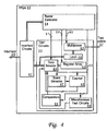
FPGA 33, and results may also be returned to processors 23A and 23B via PCI interface 26A overPCI bus 28 for display of debug information to a user. - Referring now to Figure 4, configuration of
FPGA 33 in accordance with the described embodiment is depicted.Interface 29 is coupled to interfacecircuits 41, which provide means forPCI Interface 31 to communicate withRaster Controller 34. Internal signals 50, 51 and 52 from Raster Controller are coupled to testcircuits 35. These test circuits may be varied as needed. Designs are produced via FPGA design software and binary image files are produced that may be stored within persistent storage coupled tonetwork 15, embedded within program code withinmemory 24 or selected from a configuration ram that may be optionally coupled toFPGA 33. Depending on a desired particular test or debugging sequence or a level of trace output required (sparse vs. verbose), different configurations may be loaded intoFPGA 33. - In the configuration of
FPGA 33 depicted in Figure 4,exemplary test circuits 35 are shown. Some elements may be common to all configuration images, while others are used for specific tests and debug operations. It is helpful during the debug/design phase of a peripheral device to build a library of these test circuits that can be later used for maintenance or field troubleshooting. Particular points can be selected from the functional logic and particular circuitry can be implemented withintest circuits 35 to allow troubleshooting to be a progressive process, with new configuration images developed for download to FPGA 33 until the information needed to solve a particular problem is available. A configuration providing less test detail about a particular portion of the functional logic, but general information about the entire operation of the functional logic is useful in the production cycle of a product containing test circuits. - The information that is held in
register array 42 and presented to interface 29 may also be varied as a function of error detection. For example,raster controller 34 may contain circuitry for detecting parity errors, graphics object sequence errors and graphics object type errors. Depending on the type of error detected, different subsets of internal signals 52 may be latched inregister array 42. The selection of the particular signals is based upon the type of error, in order to present the most useful information for that type of error, or all of internal signals 52 can be latched and the output format of the trace program varied to display the information in a form that assists in determining the cause of an error. The trace program output can also be transmitted overnetwork 15, allowing remote debugging. An Internet connection might be used to provide a graphical or text interface accessible from an Internet or intra-net connection. -
Data selector 44 interfaces direct signals 51 from the functional logic (Raster Controller 34) as well as data fromregister array 42, which can provide static versions of signals 52 fromRaster Controller 34.Data selector 44 also selects data from specialised test circuits such ascomparators 45, counter 48, as well as othermiscellaneous test circuits 49.Comparators 45, provide a means for determining when specific values occur, for example producing an output when a particular data value or address is processed byRaster Controller 34.Event Detector 47 may detect a particular combination of logic signals 53 fromRaster Controller 34.Counter 48 can be configured to count how many events detectable byevent detector 47 have occurred, or may count transitions of some other clock signal, such as a data strobe between events, such as a parity error. Counters are also useful for determining the source of errors that are data dependant. For example, counters may be implemented withintest circuits 35 to determine which graphics object is being processed byraster controller 34 and precisely which values within the graphics object are being processed when the error occurs. - The output of
data selector 44 is provided throughinterface circuits 41 tointerface 29. The values selectable bydata selector 44 can thus be accessed overPCI bus 28 via PCI interface 26A and thus used by processors 23A and 23B. -
Latch 46, is provided to select test point Signals 50 for output to physical pins onFPGA 33 viaMultiplexer 43. This allows selection of real time output of signals fromRaster Controller 34 that can be used with a logic analyser, oscilloscope or other device.Multiplexer 33 can also be controlled by an external pin connection to control the selection of internal nodes output to test point signals 50, the external pins can supply the multiplexer select signals, instead of or in addition to the select signals supplied fromlatch 46. - Referring now to Figure 5, there is illustrated a flow diagram of a method for tracing hardware states using dynamically reconfigurable test circuits in accordance with an embodiment. This method is generally embodied in a software trace program running within
printer 14. - A user or software program selects a trace format (debug level) for output (step 60). A logic configuration for
FPGA 33 is selected in conformity with the trace format (step 61) and the logic configuration is loaded into FPGA 33 (step 62). Multiplexer outputs for external test points 37 are selected (step 63) to provide any external signals desired for debugging. When the trace program reaches a dump request (decision 64) the register array contents are read (step 65) and the trace program outputs them to a display or as a file, or network data. If during execution an error is detected by the trace program for which a dump request is enabled (decision 66), selected or all) register array contents are read (step 67) and output to a display or as a file or network data. The steps ofmultiplexer selection 53, and hardware tracing 54 and 56 are repeated until the trace program terminates or the printer is shut down (step 68). - Although the invention has been described with reference to specific embodiments, this description is not meant to be construed in a limiting sense. Various modifications of the disclosed embodiments, as well as alternative embodiments of the invention, will become apparent to persons skilled in the art upon reference to the description of the invention. It is therefore contemplated that such modifications can be made without departing from the scope of the present invention.
Claims (20)
- A method for tracing hardware states within a functional logic within a field programmable logic circuit using dynamically reconfigurable test circuits, said method comprising the steps of:first selecting a test mode from a plurality of test modes for tracing the operation of said functional logic;after said step of selecting a test mode, second selecting one of a plurality of configurations for said dynamically reconfigurable test circuits in conformity with said selected test mode; andconfiguring said field programmable logic circuit in using said selected configuration.
- A method as claimed in claim 1, wherein said method further comprises the steps of:tracing execution of program code to create a software trace history;periodically reading a set of registers within said dynamically reconfigurable test circuits to create a hardware trace log in response to said tracing step reaching a hardware trace request; andrecording the contents of said registers in synchronisation with said software trace history to produce a full trace history.
- A method as claimed in claim 2, wherein said step of first selecting a test mode for tracing the operation of said functional logic further selects a format for output of said hardware trace log.
- A method as claimed in claim 2 or claim 3, wherein said method further comprises the step of detecting an error associated with said functional logic, and wherein said hardware trace request is made in response to said detected error.
- A method as claimed in any one of claims 2 to 5, wherein said dynamically reconfigurable test circuits further comprise counters for counting transitions on internal signals within said functional logic, wherein said method further comprises the step of counting said transitions on internal signals, and wherein said step of periodically reading said set of registers further reads values of said counters.
- A method as claimed in claim 5, wherein said dynamically reconfigurable test circuits further comprise event detectors for detecting events occurring within said functional logic, wherein said method further comprises the step of detecting events occurring within said functional logic, and wherein said step of periodically reading said set of registers further reads values of said counters to determine the number of counts that have occurred between said events.
- A method as claimed in claim 6, wherein said event detectors are error detectors for detecting errors occurring within said functional logic and wherein said step of detecting events detects said errors.
- A method as claimed in any one of the preceding claims, wherein said method further comprises the step of transmitting said configuration image into said field programmable logic circuit to configure said dynamically reconfigurable test circuits.
- A method as claimed in claim 8, wherein said step of transmitting said configuration image is performed by writing data to said field programmable logic circuit over a peripheral bus.
- A method as claimed in any one of the preceding claims, wherein said method further comprises the step selecting a plurality of nodes within said functional logic for output to external test pins on said field programmable logic circuit.
- An apparatus having a field programmable logic circuit with functional logic, said apparatus further comprising:a plurality of test circuits implemented within said field programmable logic circuit, wherein said test circuits are instantiated by loading one of a plurality of configuration images; anda storage for storing said plurality of configuration images for configuring said field programmable logic circuit.
- An apparatus as claimed in claim 11, further comprising a bus interface coupled to said field programmable logic circuit for receiving said configuration images.
- An apparatus as claimed in claim 11 or claim 12, wherein said field programmable logic circuit includes external test pins for coupling to external test equipment, and wherein at least one of said configuration images configures said field programmable logic circuit to output signals from test nodes within said functional logic.
- An apparatus as claimed in claim 13, further comprising a bus interface coupled to said field programmable logic circuit for receiving said configuration images and for receiving a selection word that selects said test nodes from a plurality of available test nodes.
- An apparatus as claimed in claim 13, wherein said field programmable logic circuit includes external pins configured as selector pins for selecting said test nodes from a plurality of available test nodes.
- An apparatus as claimed in any one of claims 11 to 15, wherein at least one of said configuration images configures said field programmable logic circuit to include registers for providing states of signals within said functional logic, and wherein said functional logic includes an interface coupled to said registers for providing external access to said registers.
- An apparatus as claimed in claim 13, wherein said functional logic includes an error detector for detecting an error occurring within said functional logic, and wherein at least one of said configuration images configures said field programmable logic circuit to include circuitry to store information within said registers in response to said error detector detecting an error.
- A system for controlling an electronic device, comprising:functional logic implemented as a configuration within a field programmable logic circuit;a processor for executing program instructions to control said electronic device; anda storage for storing a plurality of configuration files for configuring said field programmable logic circuit, wherein said processor retrieves a first one of said plurality of configuration files and configures said field programmable logic circuit to contain test circuits by transferring said first configuration files to said field programmable logic circuit.
- A system as claimed in claim 18, wherein said processor configures said field programmable logic circuit with a test multiplexor having connections to external pins of said field programmable logic circuit for coupling signals within said functional logic to said external pins for measurement by external test equipment.
- A system as claimed in claim 18, wherein said program instructions include means for tracing execution of program code to create a software trace history, periodically reading a set of registers within said dynamically reconfigurable test circuits to create a hardware trace log in response to said tracing step reaching a hardware trace request, and recording the contents of said registers in synchronisation with said software trace history to produce a full trace history.
Applications Claiming Priority (2)
| Application Number | Priority Date | Filing Date | Title |
|---|---|---|---|
| US09/631,130 US6542844B1 (en) | 2000-08-02 | 2000-08-02 | Method and apparatus for tracing hardware states using dynamically reconfigurable test circuits |
| US631130 | 2000-08-02 |
Publications (3)
| Publication Number | Publication Date |
|---|---|
| EP1178324A2 true EP1178324A2 (en) | 2002-02-06 |
| EP1178324A3 EP1178324A3 (en) | 2004-01-07 |
| EP1178324B1 EP1178324B1 (en) | 2005-10-05 |
Family
ID=24529882
Family Applications (1)
| Application Number | Title | Priority Date | Filing Date |
|---|---|---|---|
| EP01305974A Expired - Lifetime EP1178324B1 (en) | 2000-08-02 | 2001-07-11 | Method and apparatus for tracing hardware states using dynamically reconfigurable test circuits |
Country Status (8)
| Country | Link |
|---|---|
| US (1) | US6542844B1 (en) |
| EP (1) | EP1178324B1 (en) |
| KR (1) | KR100420418B1 (en) |
| CN (1) | CN1201229C (en) |
| AT (1) | ATE306084T1 (en) |
| CA (1) | CA2354248C (en) |
| DE (1) | DE60113780T2 (en) |
| GB (1) | GB2368421A (en) |
Cited By (1)
| Publication number | Priority date | Publication date | Assignee | Title |
|---|---|---|---|---|
| KR100445636B1 (en) * | 2002-06-17 | 2004-08-25 | 삼성전자주식회사 | Computer system test device using FPGA and programmable memory modules and the test method thereof |
Families Citing this family (100)
| Publication number | Priority date | Publication date | Assignee | Title |
|---|---|---|---|---|
| US7266725B2 (en) | 2001-09-03 | 2007-09-04 | Pact Xpp Technologies Ag | Method for debugging reconfigurable architectures |
| DE19651075A1 (en) * | 1996-12-09 | 1998-06-10 | Pact Inf Tech Gmbh | Unit for processing numerical and logical operations, for use in processors (CPU's), multi-computer systems, data flow processors (DFP's), digital signal processors (DSP's) or the like |
| DE19654595A1 (en) | 1996-12-20 | 1998-07-02 | Pact Inf Tech Gmbh | I0 and memory bus system for DFPs as well as building blocks with two- or multi-dimensional programmable cell structures |
| JP3961028B2 (en) | 1996-12-27 | 2007-08-15 | ペーアーツェーテー イクスペーペー テクノロジーズ アクチエンゲゼルシャフト | Data flow processor (DFP) automatic dynamic unloading method and modules with 2D or 3D programmable cell structure (FPGA, DPGA, etc.) |
| US6542998B1 (en) | 1997-02-08 | 2003-04-01 | Pact Gmbh | Method of self-synchronization of configurable elements of a programmable module |
| US8686549B2 (en) | 2001-09-03 | 2014-04-01 | Martin Vorbach | Reconfigurable elements |
| DE19861088A1 (en) | 1997-12-22 | 2000-02-10 | Pact Inf Tech Gmbh | Repairing integrated circuits by replacing subassemblies with substitutes |
| CN1378665A (en) | 1999-06-10 | 2002-11-06 | Pact信息技术有限公司 | Programming concept |
| US6671825B1 (en) | 1999-11-19 | 2003-12-30 | Oracle International Corporation | Method and apparatus for debugging a software program |
| US6745344B1 (en) * | 1999-11-19 | 2004-06-01 | Oracle International Corporation | Debug and data collection mechanism utilizing a difference in database state by using consecutive snapshots of the database state |
| US6671826B1 (en) | 1999-11-19 | 2003-12-30 | Oracle International Corporation | Fast database state dumps to file for deferred analysis of a database |
| US6839894B1 (en) | 1999-11-19 | 2005-01-04 | Oracle International Corporation | Method and apparatus for debugging a software program using dynamic debug patches and copy on write views |
| JP2004506261A (en) | 2000-06-13 | 2004-02-26 | ペーアーツェーテー イクスペーペー テクノロジーズ アクチエンゲゼルシャフト | Pipeline CT protocol and CT communication |
| ATE437476T1 (en) * | 2000-10-06 | 2009-08-15 | Pact Xpp Technologies Ag | CELL ARRANGEMENT WITH SEGMENTED INTERCELL STRUCTURE |
| US8058899B2 (en) | 2000-10-06 | 2011-11-15 | Martin Vorbach | Logic cell array and bus system |
| US8103496B1 (en) | 2000-10-26 | 2012-01-24 | Cypress Semicondutor Corporation | Breakpoint control in an in-circuit emulation system |
| US7765095B1 (en) | 2000-10-26 | 2010-07-27 | Cypress Semiconductor Corporation | Conditional branching in an in-circuit emulation system |
| US8149048B1 (en) | 2000-10-26 | 2012-04-03 | Cypress Semiconductor Corporation | Apparatus and method for programmable power management in a programmable analog circuit block |
| US8160864B1 (en) | 2000-10-26 | 2012-04-17 | Cypress Semiconductor Corporation | In-circuit emulator and pod synchronized boot |
| US8176296B2 (en) | 2000-10-26 | 2012-05-08 | Cypress Semiconductor Corporation | Programmable microcontroller architecture |
| US6724220B1 (en) | 2000-10-26 | 2004-04-20 | Cyress Semiconductor Corporation | Programmable microcontroller architecture (mixed analog/digital) |
| US6681354B2 (en) * | 2001-01-31 | 2004-01-20 | Stmicroelectronics, Inc. | Embedded field programmable gate array for performing built-in self test functions in a system on a chip and method of operation |
| WO2005045692A2 (en) | 2003-08-28 | 2005-05-19 | Pact Xpp Technologies Ag | Data processing device and method |
| US9037807B2 (en) | 2001-03-05 | 2015-05-19 | Pact Xpp Technologies Ag | Processor arrangement on a chip including data processing, memory, and interface elements |
| US20070299993A1 (en) * | 2001-03-05 | 2007-12-27 | Pact Xpp Technologies Ag | Method and Device for Treating and Processing Data |
| US7444531B2 (en) | 2001-03-05 | 2008-10-28 | Pact Xpp Technologies Ag | Methods and devices for treating and processing data |
| US7844796B2 (en) | 2001-03-05 | 2010-11-30 | Martin Vorbach | Data processing device and method |
| ATE478381T1 (en) | 2001-06-20 | 2010-09-15 | Richter Thomas | DATA PROCESSING PROCEDURES |
| US7996827B2 (en) | 2001-08-16 | 2011-08-09 | Martin Vorbach | Method for the translation of programs for reconfigurable architectures |
| WO2003016549A2 (en) * | 2001-08-17 | 2003-02-27 | Incyte Genomics, Inc. | Nucleic-acid associated proteins |
| US7434191B2 (en) | 2001-09-03 | 2008-10-07 | Pact Xpp Technologies Ag | Router |
| US8686475B2 (en) | 2001-09-19 | 2014-04-01 | Pact Xpp Technologies Ag | Reconfigurable elements |
| US7406674B1 (en) | 2001-10-24 | 2008-07-29 | Cypress Semiconductor Corporation | Method and apparatus for generating microcontroller configuration information |
| US8078970B1 (en) | 2001-11-09 | 2011-12-13 | Cypress Semiconductor Corporation | Graphical user interface with user-selectable list-box |
| US7512931B2 (en) * | 2001-11-13 | 2009-03-31 | National Instruments Corporation | Graphical program nodes for implementing a measurement state model |
| US8042093B1 (en) | 2001-11-15 | 2011-10-18 | Cypress Semiconductor Corporation | System providing automatic source code generation for personalization and parameterization of user modules |
| US6701508B1 (en) * | 2001-11-19 | 2004-03-02 | Cypress Semiconductor Corporation | Method and system for using a graphics user interface for programming an electronic device |
| US7770113B1 (en) | 2001-11-19 | 2010-08-03 | Cypress Semiconductor Corporation | System and method for dynamically generating a configuration datasheet |
| US8069405B1 (en) | 2001-11-19 | 2011-11-29 | Cypress Semiconductor Corporation | User interface for efficiently browsing an electronic document using data-driven tabs |
| US6898703B1 (en) * | 2001-11-19 | 2005-05-24 | Cypress Semiconductor Corporation | System and method for creating a boot file utilizing a boot template |
| US7844437B1 (en) | 2001-11-19 | 2010-11-30 | Cypress Semiconductor Corporation | System and method for performing next placements and pruning of disallowed placements for programming an integrated circuit |
| US7774190B1 (en) | 2001-11-19 | 2010-08-10 | Cypress Semiconductor Corporation | Sleep and stall in an in-circuit emulation system |
| US6971004B1 (en) | 2001-11-19 | 2005-11-29 | Cypress Semiconductor Corp. | System and method of dynamically reconfiguring a programmable integrated circuit |
| WO2003060747A2 (en) | 2002-01-19 | 2003-07-24 | Pact Xpp Technologies Ag | Reconfigurable processor |
| TW548419B (en) * | 2002-02-01 | 2003-08-21 | Via Tech Inc | Circuit structure of integrated graphing function chip and its test method |
| WO2003071432A2 (en) | 2002-02-18 | 2003-08-28 | Pact Xpp Technologies Ag | Bus systems and method for reconfiguration |
| US8914590B2 (en) | 2002-08-07 | 2014-12-16 | Pact Xpp Technologies Ag | Data processing method and device |
| US8103497B1 (en) | 2002-03-28 | 2012-01-24 | Cypress Semiconductor Corporation | External interface for event architecture |
| US7308608B1 (en) | 2002-05-01 | 2007-12-11 | Cypress Semiconductor Corporation | Reconfigurable testing system and method |
| JP3934493B2 (en) * | 2002-06-28 | 2007-06-20 | 富士通株式会社 | Integrated circuit and system development method |
| US7657861B2 (en) | 2002-08-07 | 2010-02-02 | Pact Xpp Technologies Ag | Method and device for processing data |
| WO2004021176A2 (en) | 2002-08-07 | 2004-03-11 | Pact Xpp Technologies Ag | Method and device for processing data |
| WO2004038599A1 (en) | 2002-09-06 | 2004-05-06 | Pact Xpp Technologies Ag | Reconfigurable sequencer structure |
| US7761845B1 (en) | 2002-09-09 | 2010-07-20 | Cypress Semiconductor Corporation | Method for parameterizing a user module |
| KR100498451B1 (en) * | 2002-10-17 | 2005-07-01 | 삼성전자주식회사 | Method for providing an information about error of HDD, HDD therefor and information processing apparatus thereof |
| GB2395578A (en) * | 2002-11-22 | 2004-05-26 | Ibm | Fault tracing in systems with virtualization layers |
| CN100412801C (en) * | 2003-09-30 | 2008-08-20 | 三洋电机株式会社 | Processor and integrated circuit comprising reconfigurable circuit, and processing method utilizing it |
| US7310728B2 (en) * | 2003-11-24 | 2007-12-18 | Itt Manufacturing Enterprises, Inc. | Method of implementing a high-speed header bypass function |
| KR100546764B1 (en) * | 2003-12-05 | 2006-01-26 | 한국전자통신연구원 | Method and apparatus of managing reconfiguration data memory |
| US8365078B2 (en) * | 2004-01-08 | 2013-01-29 | International Business Machines Corporation | Method for multidimensional visual correlation of systems management data |
| US20050188266A1 (en) * | 2004-01-27 | 2005-08-25 | Brian Johnson | System and method using a programmable device for capturing signals from a device during testing |
| US7295049B1 (en) | 2004-03-25 | 2007-11-13 | Cypress Semiconductor Corporation | Method and circuit for rapid alignment of signals |
| JP2008523456A (en) * | 2004-05-12 | 2008-07-03 | コーニンクレッカ フィリップス エレクトロニクス エヌ ヴィ | Data processing system with trace coprocessor |
| US20060015314A1 (en) * | 2004-06-30 | 2006-01-19 | International Business Machines Corporation | Methods, systems and program products for annotating system traces with control program information and presenting annotated system traces |
| DE102004037713A1 (en) * | 2004-08-04 | 2006-03-16 | Robert Bosch Gmbh | Method, operating system and computing device for executing a computer program |
| US8069436B2 (en) | 2004-08-13 | 2011-11-29 | Cypress Semiconductor Corporation | Providing hardware independence to automate code generation of processing device firmware |
| US8286125B2 (en) | 2004-08-13 | 2012-10-09 | Cypress Semiconductor Corporation | Model for a hardware device-independent method of defining embedded firmware for programmable systems |
| US7817293B2 (en) * | 2005-01-07 | 2010-10-19 | Infoprint Solutions Company, Llc | Trace and debug tool for high speed printer systems |
| US7332976B1 (en) | 2005-02-04 | 2008-02-19 | Cypress Semiconductor Corporation | Poly-phase frequency synthesis oscillator |
| WO2006089352A1 (en) * | 2005-02-22 | 2006-08-31 | United Electrical Software P/L | Method and system for monitoring computer systems |
| US7400183B1 (en) | 2005-05-05 | 2008-07-15 | Cypress Semiconductor Corporation | Voltage controlled oscillator delay cell and method |
| US8089461B2 (en) | 2005-06-23 | 2012-01-03 | Cypress Semiconductor Corporation | Touch wake for electronic devices |
| US7650539B2 (en) * | 2005-06-30 | 2010-01-19 | Microsoft Corporation | Observing debug counter values during system operation |
| US8250503B2 (en) | 2006-01-18 | 2012-08-21 | Martin Vorbach | Hardware definition method including determining whether to implement a function as hardware or software |
| US8067948B2 (en) | 2006-03-27 | 2011-11-29 | Cypress Semiconductor Corporation | Input/output multiplexer bus |
| US7693257B2 (en) * | 2006-06-29 | 2010-04-06 | Accuray Incorporated | Treatment delivery optimization |
| US8026739B2 (en) | 2007-04-17 | 2011-09-27 | Cypress Semiconductor Corporation | System level interconnect with programmable switching |
| US7737724B2 (en) * | 2007-04-17 | 2010-06-15 | Cypress Semiconductor Corporation | Universal digital block interconnection and channel routing |
| US9564902B2 (en) | 2007-04-17 | 2017-02-07 | Cypress Semiconductor Corporation | Dynamically configurable and re-configurable data path |
| US8092083B2 (en) | 2007-04-17 | 2012-01-10 | Cypress Semiconductor Corporation | Temperature sensor with digital bandgap |
| US8130025B2 (en) | 2007-04-17 | 2012-03-06 | Cypress Semiconductor Corporation | Numerical band gap |
| US8516025B2 (en) | 2007-04-17 | 2013-08-20 | Cypress Semiconductor Corporation | Clock driven dynamic datapath chaining |
| US8040266B2 (en) | 2007-04-17 | 2011-10-18 | Cypress Semiconductor Corporation | Programmable sigma-delta analog-to-digital converter |
| US8266575B1 (en) | 2007-04-25 | 2012-09-11 | Cypress Semiconductor Corporation | Systems and methods for dynamically reconfiguring a programmable system on a chip |
| US8065653B1 (en) | 2007-04-25 | 2011-11-22 | Cypress Semiconductor Corporation | Configuration of programmable IC design elements |
| US9720805B1 (en) | 2007-04-25 | 2017-08-01 | Cypress Semiconductor Corporation | System and method for controlling a target device |
| US20080276129A1 (en) * | 2007-05-02 | 2008-11-06 | International Business Machines Corporation | Software tracing |
| US8049569B1 (en) | 2007-09-05 | 2011-11-01 | Cypress Semiconductor Corporation | Circuit and method for improving the accuracy of a crystal-less oscillator having dual-frequency modes |
| US8296092B2 (en) * | 2008-08-15 | 2012-10-23 | International Business Machines Corporation | Platform specific test for computing hardware |
| US20100100786A1 (en) * | 2008-10-17 | 2010-04-22 | International Business Machines Corporation | Serial test mode of an integrated circuit (ic) |
| US9448964B2 (en) | 2009-05-04 | 2016-09-20 | Cypress Semiconductor Corporation | Autonomous control in a programmable system |
| US7969171B1 (en) | 2010-01-06 | 2011-06-28 | General Electric Company | Test circuit and system |
| CN101976431A (en) * | 2010-11-02 | 2011-02-16 | 公安部第三研究所 | Dynamic reconfiguration technology-based universal image processing platform and implementation method thereof |
| JP6613723B2 (en) * | 2015-08-27 | 2019-12-04 | 富士ゼロックス株式会社 | Electronics |
| US10261922B2 (en) * | 2017-06-09 | 2019-04-16 | Yokogawa Electric Corporation | Field device commissioning system and field device commissioning method |
| CN108388516B (en) * | 2018-03-14 | 2021-07-23 | 上海微小卫星工程中心 | Special verification test system capable of reconstructing FPGA software |
| EP3718039B1 (en) | 2018-12-03 | 2021-08-18 | Hewlett-Packard Development Company, L.P. | Logic circuitry |
| EP3688638B1 (en) * | 2018-12-03 | 2023-01-04 | Hewlett-Packard Development Company, L.P. | Logic circuitry package |
| CN112214373B (en) * | 2020-09-17 | 2022-04-12 | 上海金仕达软件科技有限公司 | Hardware monitoring method and device and electronic equipment |
| CN114124389B (en) * | 2021-11-09 | 2023-08-11 | 国网山东省电力公司电力科学研究院 | Reconfigurable computing-based FPGA (field programmable Gate array) deployment method and system |
Citations (5)
| Publication number | Priority date | Publication date | Assignee | Title |
|---|---|---|---|---|
| US4423508A (en) * | 1980-09-19 | 1983-12-27 | Hitachi, Ltd. | Logic tracing apparatus |
| US4510572A (en) * | 1981-12-28 | 1985-04-09 | Data I/O Corporation | Signature analysis system for testing digital circuits |
| US5870410A (en) * | 1996-04-29 | 1999-02-09 | Altera Corporation | Diagnostic interface system for programmable logic system development |
| US6003150A (en) * | 1996-02-02 | 1999-12-14 | Lucent Technologies Inc. | Method for testing field programmable gate arrays |
| US6014334A (en) * | 1996-03-11 | 2000-01-11 | Altera Corporation | Sample and load scheme for observability of internal nodes in a PLD |
Family Cites Families (22)
| Publication number | Priority date | Publication date | Assignee | Title |
|---|---|---|---|---|
| US4435759A (en) * | 1981-06-15 | 1984-03-06 | International Business Machines Corporation | Hardware monitor for obtaining processor software/hardware interrelationships |
| US4847839A (en) | 1987-08-26 | 1989-07-11 | Honeywell Inc. | Digital registers with serial accessed mode control bit |
| US5452231A (en) | 1988-10-05 | 1995-09-19 | Quickturn Design Systems, Inc. | Hierarchically connected reconfigurable logic assembly |
| US5109353A (en) | 1988-12-02 | 1992-04-28 | Quickturn Systems, Incorporated | Apparatus for emulation of electronic hardware system |
| FR2648916B1 (en) | 1989-06-27 | 1991-09-06 | Cit Alcatel | PRINTED CIRCUIT CARD TEST ARRANGEMENT AND ITS APPLICATION TO THE PRINTED CIRCUIT CARD TEST FORMING A MULTIPLEXING-DEMULTIPLEXING EQUIPMENT OF DIGITAL SIGNALS |
| US5499192A (en) | 1991-10-30 | 1996-03-12 | Xilinx, Inc. | Method for generating logic modules from a high level block diagram |
| US5475830A (en) | 1992-01-31 | 1995-12-12 | Quickturn Design Systems, Inc. | Structure and method for providing a reconfigurable emulation circuit without hold time violations |
| US5475624A (en) | 1992-04-30 | 1995-12-12 | Schlumberger Technologies, Inc. | Test generation by environment emulation |
| JP2746502B2 (en) | 1992-08-20 | 1998-05-06 | 三菱電機株式会社 | Apparatus and method for manufacturing semiconductor integrated circuit device and electronic circuit device |
| US5497498A (en) * | 1992-11-05 | 1996-03-05 | Giga Operations Corporation | Video processing module using a second programmable logic device which reconfigures a first programmable logic device for data transformation |
| US5596742A (en) | 1993-04-02 | 1997-01-21 | Massachusetts Institute Of Technology | Virtual interconnections for reconfigurable logic systems |
| DE4415398C2 (en) | 1994-05-03 | 1998-07-02 | Siemens Ag | Test device for interfaces |
| US5613061A (en) | 1994-09-12 | 1997-03-18 | Verilink Corporation | Network controller with reconfigurable program logic circuits capable of performing both channel service and testing functions |
| US5640107A (en) | 1995-10-24 | 1997-06-17 | Northrop Grumman Corporation | Method for in-circuit programming of a field-programmable gate array configuration memory |
| US5654650A (en) | 1995-12-11 | 1997-08-05 | Hewlett-Packard Company | High throughput FPGA control interface |
| US5673198A (en) | 1996-03-29 | 1997-09-30 | Xilinx, Inc. | Concurrent electronic circuit design and implementation |
| JPH10222374A (en) | 1996-10-28 | 1998-08-21 | Altera Corp | Method for providing remote software technological support |
| US5946219A (en) | 1996-10-30 | 1999-08-31 | Atmel Corporation | Method and system for configuring an array of logic devices |
| US5844917A (en) | 1997-04-08 | 1998-12-01 | International Business Machines Corporation | Method for testing adapter card ASIC using reconfigurable logic |
| US5978862A (en) | 1997-08-08 | 1999-11-02 | Toshiba America Information Systems, Inc. | PCMCIA card dynamically configured in first mode to program FPGA controlling application specific circuit and in second mode to operate as an I/O device |
| US6286114B1 (en) * | 1997-10-27 | 2001-09-04 | Altera Corporation | Enhanced embedded logic analyzer |
| US6016563A (en) * | 1997-12-30 | 2000-01-18 | Fleisher; Evgeny G. | Method and apparatus for testing a logic design of a programmable logic device |
-
2000
- 2000-08-02 US US09/631,130 patent/US6542844B1/en not_active Expired - Fee Related
-
2001
- 2001-04-27 GB GB0110357A patent/GB2368421A/en not_active Withdrawn
- 2001-07-11 AT AT01305974T patent/ATE306084T1/en not_active IP Right Cessation
- 2001-07-11 DE DE60113780T patent/DE60113780T2/en not_active Expired - Lifetime
- 2001-07-11 EP EP01305974A patent/EP1178324B1/en not_active Expired - Lifetime
- 2001-07-20 KR KR10-2001-0043680A patent/KR100420418B1/en not_active IP Right Cessation
- 2001-07-27 CA CA002354248A patent/CA2354248C/en not_active Expired - Fee Related
- 2001-08-01 CN CNB011247428A patent/CN1201229C/en not_active Expired - Fee Related
Patent Citations (5)
| Publication number | Priority date | Publication date | Assignee | Title |
|---|---|---|---|---|
| US4423508A (en) * | 1980-09-19 | 1983-12-27 | Hitachi, Ltd. | Logic tracing apparatus |
| US4510572A (en) * | 1981-12-28 | 1985-04-09 | Data I/O Corporation | Signature analysis system for testing digital circuits |
| US6003150A (en) * | 1996-02-02 | 1999-12-14 | Lucent Technologies Inc. | Method for testing field programmable gate arrays |
| US6014334A (en) * | 1996-03-11 | 2000-01-11 | Altera Corporation | Sample and load scheme for observability of internal nodes in a PLD |
| US5870410A (en) * | 1996-04-29 | 1999-02-09 | Altera Corporation | Diagnostic interface system for programmable logic system development |
Cited By (1)
| Publication number | Priority date | Publication date | Assignee | Title |
|---|---|---|---|---|
| KR100445636B1 (en) * | 2002-06-17 | 2004-08-25 | 삼성전자주식회사 | Computer system test device using FPGA and programmable memory modules and the test method thereof |
Also Published As
| Publication number | Publication date |
|---|---|
| KR20020011870A (en) | 2002-02-09 |
| DE60113780D1 (en) | 2005-11-10 |
| KR100420418B1 (en) | 2004-03-04 |
| US6542844B1 (en) | 2003-04-01 |
| ATE306084T1 (en) | 2005-10-15 |
| GB0110357D0 (en) | 2001-06-20 |
| CA2354248C (en) | 2006-09-19 |
| CN1336588A (en) | 2002-02-20 |
| EP1178324A3 (en) | 2004-01-07 |
| CA2354248A1 (en) | 2002-02-02 |
| GB2368421A (en) | 2002-05-01 |
| DE60113780T2 (en) | 2006-06-22 |
| EP1178324B1 (en) | 2005-10-05 |
| CN1201229C (en) | 2005-05-11 |
Similar Documents
| Publication | Publication Date | Title |
|---|---|---|
| EP1178324B1 (en) | Method and apparatus for tracing hardware states using dynamically reconfigurable test circuits | |
| US7219265B2 (en) | System and method for debugging system-on-chips | |
| EP0919916B1 (en) | Embedded logic analyzer | |
| US6247147B1 (en) | Enhanced embedded logic analyzer | |
| US6931572B1 (en) | Design instrumentation circuitry | |
| US6581191B1 (en) | Hardware debugging in a hardware description language | |
| US7072818B1 (en) | Method and system for debugging an electronic system | |
| US8516304B2 (en) | Integrated circuit including a programmable logic analyzer with enhanced analyzing and debugging capabilities and a method therefor | |
| US7055117B2 (en) | System and method for debugging system-on-chips using single or n-cycle stepping | |
| US20040025122A1 (en) | Hardware-based HDL code coverage and design analysis | |
| US6829751B1 (en) | Diagnostic architecture using FPGA core in system on a chip design | |
| US9170901B2 (en) | System and method for analyzing an electronics device including a logic analyzer | |
| US8745447B2 (en) | System and method for analyzing an electronics device including a logic analyzer | |
| US7457987B2 (en) | Test vector manager, method of managing test vectors and a test tool employing the manager and the method | |
| US7076708B2 (en) | Method and apparatus for diagnosis and behavior modification of an embedded microcontroller | |
| EP1233341B1 (en) | Embedded logic analyser | |
| US20160282408A1 (en) | Integrated Circuit Including a Programmable Logic Analyzer with Enhanced and Debugging Capabilities and a Method Therefor | |
| Jones et al. | User-centric digital test architecture | |
| Clark et al. | An Embedded Test and Configuration Processor for Self-Testable and Field Re-Configurable Systems | |
| US20030115523A1 (en) | Apparatus and method for analysis and troubleshooting of electronic devices |
Legal Events
| Date | Code | Title | Description |
|---|---|---|---|
| PUAI | Public reference made under article 153(3) epc to a published international application that has entered the european phase |
Free format text: ORIGINAL CODE: 0009012 |
|
| AK | Designated contracting states |
Kind code of ref document: A2 Designated state(s): AT BE CH CY DE DK ES FI FR GB GR IE IT LI LU MC NL PT SE TR |
|
| AX | Request for extension of the european patent |
Free format text: AL;LT;LV;MK;RO;SI |
|
| PUAL | Search report despatched |
Free format text: ORIGINAL CODE: 0009013 |
|
| AK | Designated contracting states |
Kind code of ref document: A3 Designated state(s): AT BE CH CY DE DK ES FI FR GB GR IE IT LI LU MC NL PT SE TR |
|
| AX | Request for extension of the european patent |
Extension state: AL LT LV MK RO SI |
|
| 17P | Request for examination filed |
Effective date: 20040206 |
|
| 17Q | First examination report despatched |
Effective date: 20040316 |
|
| AKX | Designation fees paid |
Designated state(s): AT BE CH CY DE DK ES FI FR GB GR IE IT LI LU MC NL PT SE TR |
|
| GRAP | Despatch of communication of intention to grant a patent |
Free format text: ORIGINAL CODE: EPIDOSNIGR1 |
|
| GRAS | Grant fee paid |
Free format text: ORIGINAL CODE: EPIDOSNIGR3 |
|
| GRAA | (expected) grant |
Free format text: ORIGINAL CODE: 0009210 |
|
| AK | Designated contracting states |
Kind code of ref document: B1 Designated state(s): AT BE CH CY DE DK ES FI FR GB GR IE IT LI LU MC NL PT SE TR |
|
| PG25 | Lapsed in a contracting state [announced via postgrant information from national office to epo] |
Ref country code: FI Free format text: LAPSE BECAUSE OF FAILURE TO SUBMIT A TRANSLATION OF THE DESCRIPTION OR TO PAY THE FEE WITHIN THE PRESCRIBED TIME-LIMIT Effective date: 20051005 Ref country code: IT Free format text: LAPSE BECAUSE OF FAILURE TO SUBMIT A TRANSLATION OF THE DESCRIPTION OR TO PAY THE FEE WITHIN THE PRESCRIBED TIME-LIMIT;WARNING: LAPSES OF ITALIAN PATENTS WITH EFFECTIVE DATE BEFORE 2007 MAY HAVE OCCURRED AT ANY TIME BEFORE 2007. THE CORRECT EFFECTIVE DATE MAY BE DIFFERENT FROM THE ONE RECORDED. Effective date: 20051005 Ref country code: NL Free format text: LAPSE BECAUSE OF FAILURE TO SUBMIT A TRANSLATION OF THE DESCRIPTION OR TO PAY THE FEE WITHIN THE PRESCRIBED TIME-LIMIT Effective date: 20051005 Ref country code: BE Free format text: LAPSE BECAUSE OF FAILURE TO SUBMIT A TRANSLATION OF THE DESCRIPTION OR TO PAY THE FEE WITHIN THE PRESCRIBED TIME-LIMIT Effective date: 20051005 Ref country code: CH Free format text: LAPSE BECAUSE OF FAILURE TO SUBMIT A TRANSLATION OF THE DESCRIPTION OR TO PAY THE FEE WITHIN THE PRESCRIBED TIME-LIMIT Effective date: 20051005 Ref country code: AT Free format text: LAPSE BECAUSE OF FAILURE TO SUBMIT A TRANSLATION OF THE DESCRIPTION OR TO PAY THE FEE WITHIN THE PRESCRIBED TIME-LIMIT Effective date: 20051005 Ref country code: LI Free format text: LAPSE BECAUSE OF FAILURE TO SUBMIT A TRANSLATION OF THE DESCRIPTION OR TO PAY THE FEE WITHIN THE PRESCRIBED TIME-LIMIT Effective date: 20051005 |
|
| REG | Reference to a national code |
Ref country code: GB Ref legal event code: FG4D |
|
| REG | Reference to a national code |
Ref country code: CH Ref legal event code: NV Representative=s name: INTERNATIONAL BUSINESS MACHINES CORPORATION Ref country code: CH Ref legal event code: EP |
|
| REG | Reference to a national code |
Ref country code: IE Ref legal event code: FG4D |
|
| REF | Corresponds to: |
Ref document number: 60113780 Country of ref document: DE Date of ref document: 20051110 Kind code of ref document: P |
|
| PG25 | Lapsed in a contracting state [announced via postgrant information from national office to epo] |
Ref country code: GR Free format text: LAPSE BECAUSE OF FAILURE TO SUBMIT A TRANSLATION OF THE DESCRIPTION OR TO PAY THE FEE WITHIN THE PRESCRIBED TIME-LIMIT Effective date: 20060105 Ref country code: SE Free format text: LAPSE BECAUSE OF FAILURE TO SUBMIT A TRANSLATION OF THE DESCRIPTION OR TO PAY THE FEE WITHIN THE PRESCRIBED TIME-LIMIT Effective date: 20060105 Ref country code: DK Free format text: LAPSE BECAUSE OF FAILURE TO SUBMIT A TRANSLATION OF THE DESCRIPTION OR TO PAY THE FEE WITHIN THE PRESCRIBED TIME-LIMIT Effective date: 20060105 |
|
| PG25 | Lapsed in a contracting state [announced via postgrant information from national office to epo] |
Ref country code: ES Free format text: LAPSE BECAUSE OF FAILURE TO SUBMIT A TRANSLATION OF THE DESCRIPTION OR TO PAY THE FEE WITHIN THE PRESCRIBED TIME-LIMIT Effective date: 20060116 |
|
| NLV1 | Nl: lapsed or annulled due to failure to fulfill the requirements of art. 29p and 29m of the patents act | ||
| PG25 | Lapsed in a contracting state [announced via postgrant information from national office to epo] |
Ref country code: PT Free format text: LAPSE BECAUSE OF FAILURE TO SUBMIT A TRANSLATION OF THE DESCRIPTION OR TO PAY THE FEE WITHIN THE PRESCRIBED TIME-LIMIT Effective date: 20060306 |
|
| REG | Reference to a national code |
Ref country code: CH Ref legal event code: PL |
|
| ET | Fr: translation filed | ||
| PG25 | Lapsed in a contracting state [announced via postgrant information from national office to epo] |
Ref country code: MC Free format text: LAPSE BECAUSE OF NON-PAYMENT OF DUE FEES Effective date: 20060731 |
|
| PLBE | No opposition filed within time limit |
Free format text: ORIGINAL CODE: 0009261 |
|
| STAA | Information on the status of an ep patent application or granted ep patent |
Free format text: STATUS: NO OPPOSITION FILED WITHIN TIME LIMIT |
|
| 26N | No opposition filed |
Effective date: 20060706 |
|
| REG | Reference to a national code |
Ref country code: GB Ref legal event code: 746 Effective date: 20080704 |
|
| PG25 | Lapsed in a contracting state [announced via postgrant information from national office to epo] |
Ref country code: TR Free format text: LAPSE BECAUSE OF FAILURE TO SUBMIT A TRANSLATION OF THE DESCRIPTION OR TO PAY THE FEE WITHIN THE PRESCRIBED TIME-LIMIT Effective date: 20051005 Ref country code: LU Free format text: LAPSE BECAUSE OF NON-PAYMENT OF DUE FEES Effective date: 20060711 |
|
| PG25 | Lapsed in a contracting state [announced via postgrant information from national office to epo] |
Ref country code: CY Free format text: LAPSE BECAUSE OF FAILURE TO SUBMIT A TRANSLATION OF THE DESCRIPTION OR TO PAY THE FEE WITHIN THE PRESCRIBED TIME-LIMIT Effective date: 20051005 |
|
| PGFP | Annual fee paid to national office [announced via postgrant information from national office to epo] |
Ref country code: IE Payment date: 20110627 Year of fee payment: 11 |
|
| PGFP | Annual fee paid to national office [announced via postgrant information from national office to epo] |
Ref country code: FR Payment date: 20110801 Year of fee payment: 11 |
|
| REG | Reference to a national code |
Ref country code: FR Ref legal event code: ST Effective date: 20130329 |
|
| PG25 | Lapsed in a contracting state [announced via postgrant information from national office to epo] |
Ref country code: FR Free format text: LAPSE BECAUSE OF NON-PAYMENT OF DUE FEES Effective date: 20120731 |
|
| REG | Reference to a national code |
Ref country code: IE Ref legal event code: MM4A |
|
| PG25 | Lapsed in a contracting state [announced via postgrant information from national office to epo] |
Ref country code: IE Free format text: LAPSE BECAUSE OF NON-PAYMENT OF DUE FEES Effective date: 20120711 |
|
| PGFP | Annual fee paid to national office [announced via postgrant information from national office to epo] |
Ref country code: GB Payment date: 20170728 Year of fee payment: 17 Ref country code: DE Payment date: 20170718 Year of fee payment: 17 |
|
| REG | Reference to a national code |
Ref country code: DE Ref legal event code: R119 Ref document number: 60113780 Country of ref document: DE |
|
| GBPC | Gb: european patent ceased through non-payment of renewal fee |
Effective date: 20180711 |
|
| PG25 | Lapsed in a contracting state [announced via postgrant information from national office to epo] |
Ref country code: GB Free format text: LAPSE BECAUSE OF NON-PAYMENT OF DUE FEES Effective date: 20180711 Ref country code: DE Free format text: LAPSE BECAUSE OF NON-PAYMENT OF DUE FEES Effective date: 20190201 |