EP1187203A2 - A semiconductor device and method of manufacturing the same - Google Patents
A semiconductor device and method of manufacturing the same Download PDFInfo
- Publication number
- EP1187203A2 EP1187203A2 EP20010302549 EP01302549A EP1187203A2 EP 1187203 A2 EP1187203 A2 EP 1187203A2 EP 20010302549 EP20010302549 EP 20010302549 EP 01302549 A EP01302549 A EP 01302549A EP 1187203 A2 EP1187203 A2 EP 1187203A2
- Authority
- EP
- European Patent Office
- Prior art keywords
- semiconductor chip
- electrode
- bonding
- radiation
- insulating
- Prior art date
- Legal status (The legal status is an assumption and is not a legal conclusion. Google has not performed a legal analysis and makes no representation as to the accuracy of the status listed.)
- Withdrawn
Links
Images


Classifications
-
- H—ELECTRICITY
- H01—ELECTRIC ELEMENTS
- H01L—SEMICONDUCTOR DEVICES NOT COVERED BY CLASS H10
- H01L23/00—Details of semiconductor or other solid state devices
- H01L23/34—Arrangements for cooling, heating, ventilating or temperature compensation ; Temperature sensing arrangements
- H01L23/36—Selection of materials, or shaping, to facilitate cooling or heating, e.g. heatsinks
-
- H—ELECTRICITY
- H01—ELECTRIC ELEMENTS
- H01L—SEMICONDUCTOR DEVICES NOT COVERED BY CLASS H10
- H01L24/00—Arrangements for connecting or disconnecting semiconductor or solid-state bodies; Methods or apparatus related thereto
- H01L24/80—Methods for connecting semiconductor or other solid state bodies using means for bonding being attached to, or being formed on, the surface to be connected
- H01L24/83—Methods for connecting semiconductor or other solid state bodies using means for bonding being attached to, or being formed on, the surface to be connected using a layer connector
-
- H—ELECTRICITY
- H01—ELECTRIC ELEMENTS
- H01L—SEMICONDUCTOR DEVICES NOT COVERED BY CLASS H10
- H01L21/00—Processes or apparatus adapted for the manufacture or treatment of semiconductor or solid state devices or of parts thereof
- H01L21/02—Manufacture or treatment of semiconductor devices or of parts thereof
- H01L21/04—Manufacture or treatment of semiconductor devices or of parts thereof the devices having at least one potential-jump barrier or surface barrier, e.g. PN junction, depletion layer or carrier concentration layer
- H01L21/48—Manufacture or treatment of parts, e.g. containers, prior to assembly of the devices, using processes not provided for in a single one of the subgroups H01L21/06 - H01L21/326
- H01L21/4814—Conductive parts
- H01L21/4821—Flat leads, e.g. lead frames with or without insulating supports
- H01L21/4828—Etching
- H01L21/4832—Etching a temporary substrate after encapsulation process to form leads
-
- H—ELECTRICITY
- H01—ELECTRIC ELEMENTS
- H01L—SEMICONDUCTOR DEVICES NOT COVERED BY CLASS H10
- H01L23/00—Details of semiconductor or other solid state devices
- H01L23/28—Encapsulations, e.g. encapsulating layers, coatings, e.g. for protection
- H01L23/31—Encapsulations, e.g. encapsulating layers, coatings, e.g. for protection characterised by the arrangement or shape
- H01L23/3107—Encapsulations, e.g. encapsulating layers, coatings, e.g. for protection characterised by the arrangement or shape the device being completely enclosed
-
- H—ELECTRICITY
- H01—ELECTRIC ELEMENTS
- H01L—SEMICONDUCTOR DEVICES NOT COVERED BY CLASS H10
- H01L23/00—Details of semiconductor or other solid state devices
- H01L23/48—Arrangements for conducting electric current to or from the solid state body in operation, e.g. leads, terminal arrangements ; Selection of materials therefor
- H01L23/488—Arrangements for conducting electric current to or from the solid state body in operation, e.g. leads, terminal arrangements ; Selection of materials therefor consisting of soldered or bonded constructions
- H01L23/495—Lead-frames or other flat leads
- H01L23/49503—Lead-frames or other flat leads characterised by the die pad
- H01L23/49513—Lead-frames or other flat leads characterised by the die pad having bonding material between chip and die pad
-
- H—ELECTRICITY
- H01—ELECTRIC ELEMENTS
- H01L—SEMICONDUCTOR DEVICES NOT COVERED BY CLASS H10
- H01L24/00—Arrangements for connecting or disconnecting semiconductor or solid-state bodies; Methods or apparatus related thereto
- H01L24/01—Means for bonding being attached to, or being formed on, the surface to be connected, e.g. chip-to-package, die-attach, "first-level" interconnects; Manufacturing methods related thereto
- H01L24/26—Layer connectors, e.g. plate connectors, solder or adhesive layers; Manufacturing methods related thereto
- H01L24/28—Structure, shape, material or disposition of the layer connectors prior to the connecting process
- H01L24/29—Structure, shape, material or disposition of the layer connectors prior to the connecting process of an individual layer connector
-
- H—ELECTRICITY
- H01—ELECTRIC ELEMENTS
- H01L—SEMICONDUCTOR DEVICES NOT COVERED BY CLASS H10
- H01L24/00—Arrangements for connecting or disconnecting semiconductor or solid-state bodies; Methods or apparatus related thereto
- H01L24/01—Means for bonding being attached to, or being formed on, the surface to be connected, e.g. chip-to-package, die-attach, "first-level" interconnects; Manufacturing methods related thereto
- H01L24/26—Layer connectors, e.g. plate connectors, solder or adhesive layers; Manufacturing methods related thereto
- H01L24/31—Structure, shape, material or disposition of the layer connectors after the connecting process
- H01L24/32—Structure, shape, material or disposition of the layer connectors after the connecting process of an individual layer connector
-
- H—ELECTRICITY
- H01—ELECTRIC ELEMENTS
- H01L—SEMICONDUCTOR DEVICES NOT COVERED BY CLASS H10
- H01L24/00—Arrangements for connecting or disconnecting semiconductor or solid-state bodies; Methods or apparatus related thereto
- H01L24/93—Batch processes
- H01L24/95—Batch processes at chip-level, i.e. with connecting carried out on a plurality of singulated devices, i.e. on diced chips
- H01L24/97—Batch processes at chip-level, i.e. with connecting carried out on a plurality of singulated devices, i.e. on diced chips the devices being connected to a common substrate, e.g. interposer, said common substrate being separable into individual assemblies after connecting
-
- H—ELECTRICITY
- H01—ELECTRIC ELEMENTS
- H01L—SEMICONDUCTOR DEVICES NOT COVERED BY CLASS H10
- H01L2221/00—Processes or apparatus adapted for the manufacture or treatment of semiconductor or solid state devices or of parts thereof covered by H01L21/00
- H01L2221/67—Apparatus for handling semiconductor or electric solid state devices during manufacture or treatment thereof; Apparatus for handling wafers during manufacture or treatment of semiconductor or electric solid state devices or components; Apparatus not specifically provided for elsewhere
- H01L2221/683—Apparatus for handling semiconductor or electric solid state devices during manufacture or treatment thereof; Apparatus for handling wafers during manufacture or treatment of semiconductor or electric solid state devices or components; Apparatus not specifically provided for elsewhere for supporting or gripping
- H01L2221/68304—Apparatus for handling semiconductor or electric solid state devices during manufacture or treatment thereof; Apparatus for handling wafers during manufacture or treatment of semiconductor or electric solid state devices or components; Apparatus not specifically provided for elsewhere for supporting or gripping using temporarily an auxiliary support
- H01L2221/68377—Apparatus for handling semiconductor or electric solid state devices during manufacture or treatment thereof; Apparatus for handling wafers during manufacture or treatment of semiconductor or electric solid state devices or components; Apparatus not specifically provided for elsewhere for supporting or gripping using temporarily an auxiliary support with parts of the auxiliary support remaining in the finished device
-
- H—ELECTRICITY
- H01—ELECTRIC ELEMENTS
- H01L—SEMICONDUCTOR DEVICES NOT COVERED BY CLASS H10
- H01L2224/00—Indexing scheme for arrangements for connecting or disconnecting semiconductor or solid-state bodies and methods related thereto as covered by H01L24/00
- H01L2224/01—Means for bonding being attached to, or being formed on, the surface to be connected, e.g. chip-to-package, die-attach, "first-level" interconnects; Manufacturing methods related thereto
- H01L2224/02—Bonding areas; Manufacturing methods related thereto
- H01L2224/04—Structure, shape, material or disposition of the bonding areas prior to the connecting process
- H01L2224/05—Structure, shape, material or disposition of the bonding areas prior to the connecting process of an individual bonding area
- H01L2224/0554—External layer
- H01L2224/0555—Shape
- H01L2224/05552—Shape in top view
- H01L2224/05554—Shape in top view being square
-
- H—ELECTRICITY
- H01—ELECTRIC ELEMENTS
- H01L—SEMICONDUCTOR DEVICES NOT COVERED BY CLASS H10
- H01L2224/00—Indexing scheme for arrangements for connecting or disconnecting semiconductor or solid-state bodies and methods related thereto as covered by H01L24/00
- H01L2224/01—Means for bonding being attached to, or being formed on, the surface to be connected, e.g. chip-to-package, die-attach, "first-level" interconnects; Manufacturing methods related thereto
- H01L2224/26—Layer connectors, e.g. plate connectors, solder or adhesive layers; Manufacturing methods related thereto
- H01L2224/28—Structure, shape, material or disposition of the layer connectors prior to the connecting process
- H01L2224/29—Structure, shape, material or disposition of the layer connectors prior to the connecting process of an individual layer connector
- H01L2224/29001—Core members of the layer connector
- H01L2224/29099—Material
- H01L2224/2919—Material with a principal constituent of the material being a polymer, e.g. polyester, phenolic based polymer, epoxy
-
- H—ELECTRICITY
- H01—ELECTRIC ELEMENTS
- H01L—SEMICONDUCTOR DEVICES NOT COVERED BY CLASS H10
- H01L2224/00—Indexing scheme for arrangements for connecting or disconnecting semiconductor or solid-state bodies and methods related thereto as covered by H01L24/00
- H01L2224/01—Means for bonding being attached to, or being formed on, the surface to be connected, e.g. chip-to-package, die-attach, "first-level" interconnects; Manufacturing methods related thereto
- H01L2224/26—Layer connectors, e.g. plate connectors, solder or adhesive layers; Manufacturing methods related thereto
- H01L2224/31—Structure, shape, material or disposition of the layer connectors after the connecting process
- H01L2224/32—Structure, shape, material or disposition of the layer connectors after the connecting process of an individual layer connector
- H01L2224/3205—Shape
- H01L2224/32057—Shape in side view
-
- H—ELECTRICITY
- H01—ELECTRIC ELEMENTS
- H01L—SEMICONDUCTOR DEVICES NOT COVERED BY CLASS H10
- H01L2224/00—Indexing scheme for arrangements for connecting or disconnecting semiconductor or solid-state bodies and methods related thereto as covered by H01L24/00
- H01L2224/01—Means for bonding being attached to, or being formed on, the surface to be connected, e.g. chip-to-package, die-attach, "first-level" interconnects; Manufacturing methods related thereto
- H01L2224/26—Layer connectors, e.g. plate connectors, solder or adhesive layers; Manufacturing methods related thereto
- H01L2224/31—Structure, shape, material or disposition of the layer connectors after the connecting process
- H01L2224/32—Structure, shape, material or disposition of the layer connectors after the connecting process of an individual layer connector
- H01L2224/321—Disposition
- H01L2224/32151—Disposition the layer connector connecting between a semiconductor or solid-state body and an item not being a semiconductor or solid-state body, e.g. chip-to-substrate, chip-to-passive
- H01L2224/32221—Disposition the layer connector connecting between a semiconductor or solid-state body and an item not being a semiconductor or solid-state body, e.g. chip-to-substrate, chip-to-passive the body and the item being stacked
- H01L2224/32225—Disposition the layer connector connecting between a semiconductor or solid-state body and an item not being a semiconductor or solid-state body, e.g. chip-to-substrate, chip-to-passive the body and the item being stacked the item being non-metallic, e.g. insulating substrate with or without metallisation
-
- H—ELECTRICITY
- H01—ELECTRIC ELEMENTS
- H01L—SEMICONDUCTOR DEVICES NOT COVERED BY CLASS H10
- H01L2224/00—Indexing scheme for arrangements for connecting or disconnecting semiconductor or solid-state bodies and methods related thereto as covered by H01L24/00
- H01L2224/01—Means for bonding being attached to, or being formed on, the surface to be connected, e.g. chip-to-package, die-attach, "first-level" interconnects; Manufacturing methods related thereto
- H01L2224/26—Layer connectors, e.g. plate connectors, solder or adhesive layers; Manufacturing methods related thereto
- H01L2224/31—Structure, shape, material or disposition of the layer connectors after the connecting process
- H01L2224/32—Structure, shape, material or disposition of the layer connectors after the connecting process of an individual layer connector
- H01L2224/321—Disposition
- H01L2224/32151—Disposition the layer connector connecting between a semiconductor or solid-state body and an item not being a semiconductor or solid-state body, e.g. chip-to-substrate, chip-to-passive
- H01L2224/32221—Disposition the layer connector connecting between a semiconductor or solid-state body and an item not being a semiconductor or solid-state body, e.g. chip-to-substrate, chip-to-passive the body and the item being stacked
- H01L2224/32245—Disposition the layer connector connecting between a semiconductor or solid-state body and an item not being a semiconductor or solid-state body, e.g. chip-to-substrate, chip-to-passive the body and the item being stacked the item being metallic
-
- H—ELECTRICITY
- H01—ELECTRIC ELEMENTS
- H01L—SEMICONDUCTOR DEVICES NOT COVERED BY CLASS H10
- H01L2224/00—Indexing scheme for arrangements for connecting or disconnecting semiconductor or solid-state bodies and methods related thereto as covered by H01L24/00
- H01L2224/01—Means for bonding being attached to, or being formed on, the surface to be connected, e.g. chip-to-package, die-attach, "first-level" interconnects; Manufacturing methods related thereto
- H01L2224/42—Wire connectors; Manufacturing methods related thereto
- H01L2224/44—Structure, shape, material or disposition of the wire connectors prior to the connecting process
- H01L2224/45—Structure, shape, material or disposition of the wire connectors prior to the connecting process of an individual wire connector
- H01L2224/45001—Core members of the connector
- H01L2224/45099—Material
- H01L2224/451—Material with a principal constituent of the material being a metal or a metalloid, e.g. boron (B), silicon (Si), germanium (Ge), arsenic (As), antimony (Sb), tellurium (Te) and polonium (Po), and alloys thereof
-
- H—ELECTRICITY
- H01—ELECTRIC ELEMENTS
- H01L—SEMICONDUCTOR DEVICES NOT COVERED BY CLASS H10
- H01L2224/00—Indexing scheme for arrangements for connecting or disconnecting semiconductor or solid-state bodies and methods related thereto as covered by H01L24/00
- H01L2224/01—Means for bonding being attached to, or being formed on, the surface to be connected, e.g. chip-to-package, die-attach, "first-level" interconnects; Manufacturing methods related thereto
- H01L2224/42—Wire connectors; Manufacturing methods related thereto
- H01L2224/47—Structure, shape, material or disposition of the wire connectors after the connecting process
- H01L2224/48—Structure, shape, material or disposition of the wire connectors after the connecting process of an individual wire connector
- H01L2224/4805—Shape
- H01L2224/4809—Loop shape
- H01L2224/48091—Arched
-
- H—ELECTRICITY
- H01—ELECTRIC ELEMENTS
- H01L—SEMICONDUCTOR DEVICES NOT COVERED BY CLASS H10
- H01L2224/00—Indexing scheme for arrangements for connecting or disconnecting semiconductor or solid-state bodies and methods related thereto as covered by H01L24/00
- H01L2224/01—Means for bonding being attached to, or being formed on, the surface to be connected, e.g. chip-to-package, die-attach, "first-level" interconnects; Manufacturing methods related thereto
- H01L2224/42—Wire connectors; Manufacturing methods related thereto
- H01L2224/47—Structure, shape, material or disposition of the wire connectors after the connecting process
- H01L2224/48—Structure, shape, material or disposition of the wire connectors after the connecting process of an individual wire connector
- H01L2224/481—Disposition
- H01L2224/48151—Connecting between a semiconductor or solid-state body and an item not being a semiconductor or solid-state body, e.g. chip-to-substrate, chip-to-passive
- H01L2224/48221—Connecting between a semiconductor or solid-state body and an item not being a semiconductor or solid-state body, e.g. chip-to-substrate, chip-to-passive the body and the item being stacked
- H01L2224/48225—Connecting between a semiconductor or solid-state body and an item not being a semiconductor or solid-state body, e.g. chip-to-substrate, chip-to-passive the body and the item being stacked the item being non-metallic, e.g. insulating substrate with or without metallisation
- H01L2224/48227—Connecting between a semiconductor or solid-state body and an item not being a semiconductor or solid-state body, e.g. chip-to-substrate, chip-to-passive the body and the item being stacked the item being non-metallic, e.g. insulating substrate with or without metallisation connecting the wire to a bond pad of the item
-
- H—ELECTRICITY
- H01—ELECTRIC ELEMENTS
- H01L—SEMICONDUCTOR DEVICES NOT COVERED BY CLASS H10
- H01L2224/00—Indexing scheme for arrangements for connecting or disconnecting semiconductor or solid-state bodies and methods related thereto as covered by H01L24/00
- H01L2224/01—Means for bonding being attached to, or being formed on, the surface to be connected, e.g. chip-to-package, die-attach, "first-level" interconnects; Manufacturing methods related thereto
- H01L2224/42—Wire connectors; Manufacturing methods related thereto
- H01L2224/47—Structure, shape, material or disposition of the wire connectors after the connecting process
- H01L2224/48—Structure, shape, material or disposition of the wire connectors after the connecting process of an individual wire connector
- H01L2224/481—Disposition
- H01L2224/48151—Connecting between a semiconductor or solid-state body and an item not being a semiconductor or solid-state body, e.g. chip-to-substrate, chip-to-passive
- H01L2224/48221—Connecting between a semiconductor or solid-state body and an item not being a semiconductor or solid-state body, e.g. chip-to-substrate, chip-to-passive the body and the item being stacked
- H01L2224/48245—Connecting between a semiconductor or solid-state body and an item not being a semiconductor or solid-state body, e.g. chip-to-substrate, chip-to-passive the body and the item being stacked the item being metallic
- H01L2224/48247—Connecting between a semiconductor or solid-state body and an item not being a semiconductor or solid-state body, e.g. chip-to-substrate, chip-to-passive the body and the item being stacked the item being metallic connecting the wire to a bond pad of the item
-
- H—ELECTRICITY
- H01—ELECTRIC ELEMENTS
- H01L—SEMICONDUCTOR DEVICES NOT COVERED BY CLASS H10
- H01L2224/00—Indexing scheme for arrangements for connecting or disconnecting semiconductor or solid-state bodies and methods related thereto as covered by H01L24/00
- H01L2224/01—Means for bonding being attached to, or being formed on, the surface to be connected, e.g. chip-to-package, die-attach, "first-level" interconnects; Manufacturing methods related thereto
- H01L2224/42—Wire connectors; Manufacturing methods related thereto
- H01L2224/47—Structure, shape, material or disposition of the wire connectors after the connecting process
- H01L2224/48—Structure, shape, material or disposition of the wire connectors after the connecting process of an individual wire connector
- H01L2224/484—Connecting portions
- H01L2224/48463—Connecting portions the connecting portion on the bonding area of the semiconductor or solid-state body being a ball bond
- H01L2224/48465—Connecting portions the connecting portion on the bonding area of the semiconductor or solid-state body being a ball bond the other connecting portion not on the bonding area being a wedge bond, i.e. ball-to-wedge, regular stitch
-
- H—ELECTRICITY
- H01—ELECTRIC ELEMENTS
- H01L—SEMICONDUCTOR DEVICES NOT COVERED BY CLASS H10
- H01L2224/00—Indexing scheme for arrangements for connecting or disconnecting semiconductor or solid-state bodies and methods related thereto as covered by H01L24/00
- H01L2224/01—Means for bonding being attached to, or being formed on, the surface to be connected, e.g. chip-to-package, die-attach, "first-level" interconnects; Manufacturing methods related thereto
- H01L2224/42—Wire connectors; Manufacturing methods related thereto
- H01L2224/47—Structure, shape, material or disposition of the wire connectors after the connecting process
- H01L2224/49—Structure, shape, material or disposition of the wire connectors after the connecting process of a plurality of wire connectors
- H01L2224/491—Disposition
- H01L2224/4912—Layout
- H01L2224/49171—Fan-out arrangements
-
- H—ELECTRICITY
- H01—ELECTRIC ELEMENTS
- H01L—SEMICONDUCTOR DEVICES NOT COVERED BY CLASS H10
- H01L2224/00—Indexing scheme for arrangements for connecting or disconnecting semiconductor or solid-state bodies and methods related thereto as covered by H01L24/00
- H01L2224/73—Means for bonding being of different types provided for in two or more of groups H01L2224/10, H01L2224/18, H01L2224/26, H01L2224/34, H01L2224/42, H01L2224/50, H01L2224/63, H01L2224/71
- H01L2224/732—Location after the connecting process
- H01L2224/73251—Location after the connecting process on different surfaces
- H01L2224/73265—Layer and wire connectors
-
- H—ELECTRICITY
- H01—ELECTRIC ELEMENTS
- H01L—SEMICONDUCTOR DEVICES NOT COVERED BY CLASS H10
- H01L2224/00—Indexing scheme for arrangements for connecting or disconnecting semiconductor or solid-state bodies and methods related thereto as covered by H01L24/00
- H01L2224/80—Methods for connecting semiconductor or other solid state bodies using means for bonding being attached to, or being formed on, the surface to be connected
- H01L2224/83—Methods for connecting semiconductor or other solid state bodies using means for bonding being attached to, or being formed on, the surface to be connected using a layer connector
- H01L2224/8319—Arrangement of the layer connectors prior to mounting
- H01L2224/83192—Arrangement of the layer connectors prior to mounting wherein the layer connectors are disposed only on another item or body to be connected to the semiconductor or solid-state body
-
- H—ELECTRICITY
- H01—ELECTRIC ELEMENTS
- H01L—SEMICONDUCTOR DEVICES NOT COVERED BY CLASS H10
- H01L2224/00—Indexing scheme for arrangements for connecting or disconnecting semiconductor or solid-state bodies and methods related thereto as covered by H01L24/00
- H01L2224/80—Methods for connecting semiconductor or other solid state bodies using means for bonding being attached to, or being formed on, the surface to be connected
- H01L2224/83—Methods for connecting semiconductor or other solid state bodies using means for bonding being attached to, or being formed on, the surface to be connected using a layer connector
- H01L2224/8338—Bonding interfaces outside the semiconductor or solid-state body
- H01L2224/83385—Shape, e.g. interlocking features
-
- H—ELECTRICITY
- H01—ELECTRIC ELEMENTS
- H01L—SEMICONDUCTOR DEVICES NOT COVERED BY CLASS H10
- H01L2224/00—Indexing scheme for arrangements for connecting or disconnecting semiconductor or solid-state bodies and methods related thereto as covered by H01L24/00
- H01L2224/80—Methods for connecting semiconductor or other solid state bodies using means for bonding being attached to, or being formed on, the surface to be connected
- H01L2224/83—Methods for connecting semiconductor or other solid state bodies using means for bonding being attached to, or being formed on, the surface to be connected using a layer connector
- H01L2224/838—Bonding techniques
- H01L2224/8385—Bonding techniques using a polymer adhesive, e.g. an adhesive based on silicone, epoxy, polyimide, polyester
-
- H—ELECTRICITY
- H01—ELECTRIC ELEMENTS
- H01L—SEMICONDUCTOR DEVICES NOT COVERED BY CLASS H10
- H01L2224/00—Indexing scheme for arrangements for connecting or disconnecting semiconductor or solid-state bodies and methods related thereto as covered by H01L24/00
- H01L2224/80—Methods for connecting semiconductor or other solid state bodies using means for bonding being attached to, or being formed on, the surface to be connected
- H01L2224/85—Methods for connecting semiconductor or other solid state bodies using means for bonding being attached to, or being formed on, the surface to be connected using a wire connector
- H01L2224/85001—Methods for connecting semiconductor or other solid state bodies using means for bonding being attached to, or being formed on, the surface to be connected using a wire connector involving a temporary auxiliary member not forming part of the bonding apparatus, e.g. removable or sacrificial coating, film or substrate
-
- H—ELECTRICITY
- H01—ELECTRIC ELEMENTS
- H01L—SEMICONDUCTOR DEVICES NOT COVERED BY CLASS H10
- H01L2224/00—Indexing scheme for arrangements for connecting or disconnecting semiconductor or solid-state bodies and methods related thereto as covered by H01L24/00
- H01L2224/91—Methods for connecting semiconductor or solid state bodies including different methods provided for in two or more of groups H01L2224/80 - H01L2224/90
- H01L2224/92—Specific sequence of method steps
-
- H—ELECTRICITY
- H01—ELECTRIC ELEMENTS
- H01L—SEMICONDUCTOR DEVICES NOT COVERED BY CLASS H10
- H01L2224/00—Indexing scheme for arrangements for connecting or disconnecting semiconductor or solid-state bodies and methods related thereto as covered by H01L24/00
- H01L2224/93—Batch processes
- H01L2224/95—Batch processes at chip-level, i.e. with connecting carried out on a plurality of singulated devices, i.e. on diced chips
- H01L2224/97—Batch processes at chip-level, i.e. with connecting carried out on a plurality of singulated devices, i.e. on diced chips the devices being connected to a common substrate, e.g. interposer, said common substrate being separable into individual assemblies after connecting
-
- H—ELECTRICITY
- H01—ELECTRIC ELEMENTS
- H01L—SEMICONDUCTOR DEVICES NOT COVERED BY CLASS H10
- H01L24/00—Arrangements for connecting or disconnecting semiconductor or solid-state bodies; Methods or apparatus related thereto
- H01L24/01—Means for bonding being attached to, or being formed on, the surface to be connected, e.g. chip-to-package, die-attach, "first-level" interconnects; Manufacturing methods related thereto
- H01L24/42—Wire connectors; Manufacturing methods related thereto
- H01L24/44—Structure, shape, material or disposition of the wire connectors prior to the connecting process
- H01L24/45—Structure, shape, material or disposition of the wire connectors prior to the connecting process of an individual wire connector
-
- H—ELECTRICITY
- H01—ELECTRIC ELEMENTS
- H01L—SEMICONDUCTOR DEVICES NOT COVERED BY CLASS H10
- H01L24/00—Arrangements for connecting or disconnecting semiconductor or solid-state bodies; Methods or apparatus related thereto
- H01L24/01—Means for bonding being attached to, or being formed on, the surface to be connected, e.g. chip-to-package, die-attach, "first-level" interconnects; Manufacturing methods related thereto
- H01L24/42—Wire connectors; Manufacturing methods related thereto
- H01L24/47—Structure, shape, material or disposition of the wire connectors after the connecting process
- H01L24/48—Structure, shape, material or disposition of the wire connectors after the connecting process of an individual wire connector
-
- H—ELECTRICITY
- H01—ELECTRIC ELEMENTS
- H01L—SEMICONDUCTOR DEVICES NOT COVERED BY CLASS H10
- H01L24/00—Arrangements for connecting or disconnecting semiconductor or solid-state bodies; Methods or apparatus related thereto
- H01L24/01—Means for bonding being attached to, or being formed on, the surface to be connected, e.g. chip-to-package, die-attach, "first-level" interconnects; Manufacturing methods related thereto
- H01L24/42—Wire connectors; Manufacturing methods related thereto
- H01L24/47—Structure, shape, material or disposition of the wire connectors after the connecting process
- H01L24/49—Structure, shape, material or disposition of the wire connectors after the connecting process of a plurality of wire connectors
-
- H—ELECTRICITY
- H01—ELECTRIC ELEMENTS
- H01L—SEMICONDUCTOR DEVICES NOT COVERED BY CLASS H10
- H01L24/00—Arrangements for connecting or disconnecting semiconductor or solid-state bodies; Methods or apparatus related thereto
- H01L24/73—Means for bonding being of different types provided for in two or more of groups H01L24/10, H01L24/18, H01L24/26, H01L24/34, H01L24/42, H01L24/50, H01L24/63, H01L24/71
-
- H—ELECTRICITY
- H01—ELECTRIC ELEMENTS
- H01L—SEMICONDUCTOR DEVICES NOT COVERED BY CLASS H10
- H01L2924/00—Indexing scheme for arrangements or methods for connecting or disconnecting semiconductor or solid-state bodies as covered by H01L24/00
- H01L2924/0001—Technical content checked by a classifier
- H01L2924/00014—Technical content checked by a classifier the subject-matter covered by the group, the symbol of which is combined with the symbol of this group, being disclosed without further technical details
-
- H—ELECTRICITY
- H01—ELECTRIC ELEMENTS
- H01L—SEMICONDUCTOR DEVICES NOT COVERED BY CLASS H10
- H01L2924/00—Indexing scheme for arrangements or methods for connecting or disconnecting semiconductor or solid-state bodies as covered by H01L24/00
- H01L2924/01—Chemical elements
- H01L2924/01005—Boron [B]
-
- H—ELECTRICITY
- H01—ELECTRIC ELEMENTS
- H01L—SEMICONDUCTOR DEVICES NOT COVERED BY CLASS H10
- H01L2924/00—Indexing scheme for arrangements or methods for connecting or disconnecting semiconductor or solid-state bodies as covered by H01L24/00
- H01L2924/01—Chemical elements
- H01L2924/01006—Carbon [C]
-
- H—ELECTRICITY
- H01—ELECTRIC ELEMENTS
- H01L—SEMICONDUCTOR DEVICES NOT COVERED BY CLASS H10
- H01L2924/00—Indexing scheme for arrangements or methods for connecting or disconnecting semiconductor or solid-state bodies as covered by H01L24/00
- H01L2924/01—Chemical elements
- H01L2924/01013—Aluminum [Al]
-
- H—ELECTRICITY
- H01—ELECTRIC ELEMENTS
- H01L—SEMICONDUCTOR DEVICES NOT COVERED BY CLASS H10
- H01L2924/00—Indexing scheme for arrangements or methods for connecting or disconnecting semiconductor or solid-state bodies as covered by H01L24/00
- H01L2924/01—Chemical elements
- H01L2924/01015—Phosphorus [P]
-
- H—ELECTRICITY
- H01—ELECTRIC ELEMENTS
- H01L—SEMICONDUCTOR DEVICES NOT COVERED BY CLASS H10
- H01L2924/00—Indexing scheme for arrangements or methods for connecting or disconnecting semiconductor or solid-state bodies as covered by H01L24/00
- H01L2924/01—Chemical elements
- H01L2924/01029—Copper [Cu]
-
- H—ELECTRICITY
- H01—ELECTRIC ELEMENTS
- H01L—SEMICONDUCTOR DEVICES NOT COVERED BY CLASS H10
- H01L2924/00—Indexing scheme for arrangements or methods for connecting or disconnecting semiconductor or solid-state bodies as covered by H01L24/00
- H01L2924/01—Chemical elements
- H01L2924/01033—Arsenic [As]
-
- H—ELECTRICITY
- H01—ELECTRIC ELEMENTS
- H01L—SEMICONDUCTOR DEVICES NOT COVERED BY CLASS H10
- H01L2924/00—Indexing scheme for arrangements or methods for connecting or disconnecting semiconductor or solid-state bodies as covered by H01L24/00
- H01L2924/01—Chemical elements
- H01L2924/01046—Palladium [Pd]
-
- H—ELECTRICITY
- H01—ELECTRIC ELEMENTS
- H01L—SEMICONDUCTOR DEVICES NOT COVERED BY CLASS H10
- H01L2924/00—Indexing scheme for arrangements or methods for connecting or disconnecting semiconductor or solid-state bodies as covered by H01L24/00
- H01L2924/01—Chemical elements
- H01L2924/01047—Silver [Ag]
-
- H—ELECTRICITY
- H01—ELECTRIC ELEMENTS
- H01L—SEMICONDUCTOR DEVICES NOT COVERED BY CLASS H10
- H01L2924/00—Indexing scheme for arrangements or methods for connecting or disconnecting semiconductor or solid-state bodies as covered by H01L24/00
- H01L2924/01—Chemical elements
- H01L2924/0105—Tin [Sn]
-
- H—ELECTRICITY
- H01—ELECTRIC ELEMENTS
- H01L—SEMICONDUCTOR DEVICES NOT COVERED BY CLASS H10
- H01L2924/00—Indexing scheme for arrangements or methods for connecting or disconnecting semiconductor or solid-state bodies as covered by H01L24/00
- H01L2924/01—Chemical elements
- H01L2924/01078—Platinum [Pt]
-
- H—ELECTRICITY
- H01—ELECTRIC ELEMENTS
- H01L—SEMICONDUCTOR DEVICES NOT COVERED BY CLASS H10
- H01L2924/00—Indexing scheme for arrangements or methods for connecting or disconnecting semiconductor or solid-state bodies as covered by H01L24/00
- H01L2924/01—Chemical elements
- H01L2924/01079—Gold [Au]
-
- H—ELECTRICITY
- H01—ELECTRIC ELEMENTS
- H01L—SEMICONDUCTOR DEVICES NOT COVERED BY CLASS H10
- H01L2924/00—Indexing scheme for arrangements or methods for connecting or disconnecting semiconductor or solid-state bodies as covered by H01L24/00
- H01L2924/01—Chemical elements
- H01L2924/01082—Lead [Pb]
-
- H—ELECTRICITY
- H01—ELECTRIC ELEMENTS
- H01L—SEMICONDUCTOR DEVICES NOT COVERED BY CLASS H10
- H01L2924/00—Indexing scheme for arrangements or methods for connecting or disconnecting semiconductor or solid-state bodies as covered by H01L24/00
- H01L2924/013—Alloys
- H01L2924/0132—Binary Alloys
-
- H—ELECTRICITY
- H01—ELECTRIC ELEMENTS
- H01L—SEMICONDUCTOR DEVICES NOT COVERED BY CLASS H10
- H01L2924/00—Indexing scheme for arrangements or methods for connecting or disconnecting semiconductor or solid-state bodies as covered by H01L24/00
- H01L2924/013—Alloys
- H01L2924/014—Solder alloys
-
- H—ELECTRICITY
- H01—ELECTRIC ELEMENTS
- H01L—SEMICONDUCTOR DEVICES NOT COVERED BY CLASS H10
- H01L2924/00—Indexing scheme for arrangements or methods for connecting or disconnecting semiconductor or solid-state bodies as covered by H01L24/00
- H01L2924/06—Polymers
- H01L2924/0665—Epoxy resin
-
- H—ELECTRICITY
- H01—ELECTRIC ELEMENTS
- H01L—SEMICONDUCTOR DEVICES NOT COVERED BY CLASS H10
- H01L2924/00—Indexing scheme for arrangements or methods for connecting or disconnecting semiconductor or solid-state bodies as covered by H01L24/00
- H01L2924/06—Polymers
- H01L2924/078—Adhesive characteristics other than chemical
- H01L2924/07802—Adhesive characteristics other than chemical not being an ohmic electrical conductor
-
- H—ELECTRICITY
- H01—ELECTRIC ELEMENTS
- H01L—SEMICONDUCTOR DEVICES NOT COVERED BY CLASS H10
- H01L2924/00—Indexing scheme for arrangements or methods for connecting or disconnecting semiconductor or solid-state bodies as covered by H01L24/00
- H01L2924/10—Details of semiconductor or other solid state devices to be connected
- H01L2924/11—Device type
- H01L2924/12—Passive devices, e.g. 2 terminal devices
- H01L2924/1204—Optical Diode
- H01L2924/12042—LASER
-
- H—ELECTRICITY
- H01—ELECTRIC ELEMENTS
- H01L—SEMICONDUCTOR DEVICES NOT COVERED BY CLASS H10
- H01L2924/00—Indexing scheme for arrangements or methods for connecting or disconnecting semiconductor or solid-state bodies as covered by H01L24/00
- H01L2924/10—Details of semiconductor or other solid state devices to be connected
- H01L2924/11—Device type
- H01L2924/14—Integrated circuits
-
- H—ELECTRICITY
- H01—ELECTRIC ELEMENTS
- H01L—SEMICONDUCTOR DEVICES NOT COVERED BY CLASS H10
- H01L2924/00—Indexing scheme for arrangements or methods for connecting or disconnecting semiconductor or solid-state bodies as covered by H01L24/00
- H01L2924/15—Details of package parts other than the semiconductor or other solid state devices to be connected
- H01L2924/151—Die mounting substrate
- H01L2924/153—Connection portion
- H01L2924/1531—Connection portion the connection portion being formed only on the surface of the substrate opposite to the die mounting surface
- H01L2924/15311—Connection portion the connection portion being formed only on the surface of the substrate opposite to the die mounting surface being a ball array, e.g. BGA
-
- H—ELECTRICITY
- H01—ELECTRIC ELEMENTS
- H01L—SEMICONDUCTOR DEVICES NOT COVERED BY CLASS H10
- H01L2924/00—Indexing scheme for arrangements or methods for connecting or disconnecting semiconductor or solid-state bodies as covered by H01L24/00
- H01L2924/15—Details of package parts other than the semiconductor or other solid state devices to be connected
- H01L2924/151—Die mounting substrate
- H01L2924/156—Material
- H01L2924/15786—Material with a principal constituent of the material being a non metallic, non metalloid inorganic material
- H01L2924/15787—Ceramics, e.g. crystalline carbides, nitrides or oxides
-
- H—ELECTRICITY
- H01—ELECTRIC ELEMENTS
- H01L—SEMICONDUCTOR DEVICES NOT COVERED BY CLASS H10
- H01L2924/00—Indexing scheme for arrangements or methods for connecting or disconnecting semiconductor or solid-state bodies as covered by H01L24/00
- H01L2924/15—Details of package parts other than the semiconductor or other solid state devices to be connected
- H01L2924/181—Encapsulation
- H01L2924/183—Connection portion, e.g. seal
- H01L2924/18301—Connection portion, e.g. seal being an anchoring portion, i.e. mechanical interlocking between the encapsulation resin and another package part
-
- H—ELECTRICITY
- H01—ELECTRIC ELEMENTS
- H01L—SEMICONDUCTOR DEVICES NOT COVERED BY CLASS H10
- H01L2924/00—Indexing scheme for arrangements or methods for connecting or disconnecting semiconductor or solid-state bodies as covered by H01L24/00
- H01L2924/30—Technical effects
- H01L2924/35—Mechanical effects
- H01L2924/351—Thermal stress
Definitions
- the present invention relates to a semiconductor device and a method for manufacturing the same, particularly a semiconductor device radiating excellently heat from the semiconductor device and a method for manufacturing the same.
- Fig. 9 is a structure adopting a flexible sheet 50 as an interposer board, a copper foil pattern 51 is put on the flexible sheet through adhesive, and an IC chip is fixed. There is a pad for bonding 53 formed at periphery of the IC chip as the conductive pattern 51. A pad for connecting solder ball 54 is formed through a conductive path 51B formed in one body(integrally) with the pad for bonding 53.
- the entire body is sealed with an insulating resin 58 using the flexible sheet 50 as a board.
- Symbol 57 is a bonding wire.
- the invention is carried out in view of the above problems , and intends to obtain a reliable semiconductor device having a small package and a good radiation characteristics.
- the problems are solved having a pad provided facing to a bonding electrode of a semiconductor chip, an electrode for radiation provided at an arranged area of said semiconductor chip, a insulating adhesion means provided on said electrode for radiation, said semiconductor chip fixed to said insulating adhesion means and electrically connected to said pad, and a insulating resin sealing(molding) said semiconductor chip so as to expose a back face of said pad and said insulating adhesion means and to make in one body.
- said insulating adhesion means comprises an adhesion sheet or adhesive.
- the problem is solved by providing: plural bonding pads provided so as to surround one area; external connection electrodes extended in one body with said bonding pads; an electrode for radiation provided at said one area; a insulating adhesion means provided at said electrode for radiation; a semiconductor chip fixed through said insulating adhesion means; bonding wires connecting said bonding electrodes and said bonding pads on said semiconductor chip; and a insulating resin covering said semiconductor chip, said bonding pads, said electrode for radiation, said external connection electrodes, and said bonding wires and exposing back faces of said external connection electrodes, back faces of said electrodes for radiation, and back faces of said insulating adhesion means.
- the problem is solved by providing: plural pads provided so as to surround one area; an electrode for radiation provided at said one area; a insulating adhesion means provided at said electrode for radiation; a semiconductor chip fixed through said insulating adhesion means; connecting means connecting said bonding electrodes and said pads on said semiconductor chip; and a insulating resin covering said semiconductor chip, said bonding pads, and said connection means, and exposing back faces of said bonding pads and said insulating adhesion means; wherein the back face of said bonding pads are used as the external connection electrode.
- connection means comprises a bonding wire or brazing material.
- a side face of said pad, bonding pad, or external connection electrode comprises a curved structure.
- the problem is solved by preparing a conductive foil and half-etching so that a conductive pattern is formed in projection shape;
- the problem is solved by preparing a conductive foil and half-etching so that a conductive pattern comprising at least a pad and an electrode for radiation is formed in projection shape;
- the semiconductor device By providing the semiconductor device, it is possible to transfer heat of a semiconductor chip to an electrode for radiation. As a conductive pattern including the electrode for radiation is formed without using a supporting board, it is possible to decrease cost and to make thickness of the semiconductor device thin.
- Fig. 1 is a view describing the semiconductor device of the invention.
- Fig. 2 is a view describing the method for manufacturing the semiconductor device of the invention.
- Fig. 3 is a view describing the method for manufacturing the semiconductor device of the invention.
- Fig. 4 is a view describing the method for manufacturing the semiconductor device of the invention.
- Fig. 5 is a view describing the method for manufacturing the semiconductor device of the invention.
- Fig. 6 is a view describing the method for manufacturing the semiconductor device of the invention.
- Fig. 7 is a view describing the conductive pattern used for the semiconductor device of the invention.
- Fig. 8 is a view describing the semiconductor device of the invention.
- Fig. 9 is a view describing the conventional semiconductor device.
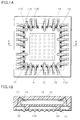
- Fig. 1A is a plan view of the semiconductor device
- Fig. 1B is a section view cut with A-A line.
- Fig. 1 shows a insulating resin 10 buried with the following chips. They are pads 11A, conductive paths 11B in one body with the pads11A, external connection electrodes 11C provided at the other ends of the conductive paths 11B in one body with the conductive paths 11B. Further an electrode for radiating 11D provided at one area surrounded by the conductive patterns 11A, 11B, and 11C and a semiconductor chip 12 provided on the electrode for radiating 11D are buried. The semiconductor chip 12 is fixed to the electrode for radiating 11D through a insulating adhesion means AD, and is shown with dotted line in Fig. 1A.
- a bonding electrode 13 of the semiconductor chip 12 and the pad 11A are electrically connected through a bonding wire 14.
- Side face of said conductive pattern 11A to 11D is etched with non-anisotropy, and has a curved structure because of being formed with wet etching so as to generate anchor effect by the curved structure.
- the structure consists of four materials: the semiconductor chip 12, plural conductive patterns 11A to 11C, the electrode for radiation 11D, the insulating adhesion means AD, and the insulating resin 10 burying them.
- said insulating adhesion means AD is formed on and between the conductive patterns 11A to 11D, particularly is provided in the isolation trench 15 formed by etching so as to expose the back face.
- the insulating resin 10 seals all including these materials. Said pads 11A and semiconductor chip 12 are supported by the insulating resin 10.
- insulating adhesion means adhesive comprising insulating material and insulating sheet of adhesiveness are desirable.
- material is desirable to bond entire wafer and to pattern by photolithography.
- thermosetting resin such as epoxy resin and thermoplastic resin such as polyimide resin and polyphenylenesulfide are used. All kinds of resin are used if they are resins hardening using a die and covering by dipping and painting.
- conductive patterns 11A to 11D conductive foil of Cu as main material, conductive foil of A1 as main material, Fe-Ni alloy, laminated product of Cu-Al, or laminated product of Al-Cu-Al is used.
- conductive material easy to etch and easy to evaporate by laser is desirable.
- conductive material of Cu as main material formed by rolling is desirable.
- the invention has a characteristic to prevent remove of the conductive pattern because the insulating resin 10 and the insulating adhesion means AD are filled into even said isolation trench 15.
- non-anisotropic etching using dry etching or wet etching for etching, the side faces of pads 11A are made into curved structure so as to generate anchor effect.
- the structure that the conductive patterns 11A to 11D do not come out (remove) from the insulating resin 10(package) is realized.
- the back faces of the conductive patterns 11A to 11D expose at the back face of the package. Accordingly the back face of the electrode 11D for radiation is fixed with the electrode on the mounting board.
- the structure can radiate heat generating from the semiconductor chip 12 on the electrode of the mounting board, can prevent temperature rise of the semiconductor chip 12, and can increase driving current of the semiconductor chip 12.
- the electrode for radiation 11C and the semiconductor chip 12 may be connected electrically.
- the conductive patterns 11A to 11D are supported by insulating resin 10 in the semiconductor device, a supporting board is not need.
- This construction is a characteristic of the invention.
- the conductive path of the conventional semiconductor device is supported by a supporting board (flexible sheet, printed board, or ceramic board), or supported by a lead frame, the construction which is not need originally is added.
- the circuit device consists of necessary minimum components and does not need the supporting board so that the device has a characteristic to be thin, light, and inexpensive because of low material cost.
- the conductive patterns 11A to 11D expose.
- brazing material such as solder for example
- the brazing material can get wet thickly because area of the electrode for radiation 11D is broad. Therefore brazing material of the back face of the external connection electrode 11C is not wet at the electrode of the mounting board at fixing on the mounting board, so it is assumed to become bad connection.
- a insulating film 16 is formed at the back face of the semiconductor device 15.
- Circles of dotted line shown Fig. 1A show the external connection electrodes 11C and electrodes for radiation 11D exposing from the insulating film 16. That is, as the insulating film 16 covers portions except the circles and size of circle portions is substantially same size, thickness of brazing material formed here is substantially same. This is similar as after solder printing and after reflow. This is similar about conductive paste such as Ag, Au, Ag-Au, Ag-Pd and so on. By the structure, bad quality of the electrical connection means 23 are depressed.
- An exposing portion 17 of the electrode for radiation 11D may be formed larger than exposing size of the external connection electrode 11C considering radiation of the semiconductor chip. As all of the external connection electrodes 11C are substantially same size, all area of the external connection electrodes 11C may be exposed at entire area, and a part of the back face of the electrode for radiation 11D may be exposed from the insulating film 16 with substantially same size.
- the insulating film 16 By providing the insulating film 16, it is possible to extend the conductive path provided at the mounting board to the back face of the semiconductor device. Although the conductive path provided at the mounting board side is generally arranged going around the fixed area of said semiconductor device, forming said insulating film 16 can arrange without going around. Further as the insulating resin 10 and the insulating adhesion means AD project from the conductive pattern, a gap is formed between the conductive path of the mounting board side and the conductive pattern so as to prevent short.
- the method for manufacturing shows the method for manufacturing of the semiconductor chip 15 shown in Fig. 1, and Fig. 2 to Fig. 6 are section views corresponding to A-A line of Fig. 1A.
- a conductive foil 20 is provided as Fig. 2. Thickness thereof is desirably 10 ⁇ m to 300 ⁇ m, here rolled copper foil of 70 ⁇ m is used.
- a conductive film 21 or a photo resist is formed as etching-resist.
- the pattern is same pattern as the pads 11A in Fig.1A, the conductive paths 11B, the external connection electrode 11C, and the electrodes for radiation 11D.
- a conductive film such as Au, Ag, Pd or Ni is formed at a part corresponding to at least pad in the lower layer of the photo resist. This is provided to make bonding possible. (Refer Fig. 2 about the above.)
- a conductive foil 20 is half-etched through said conductive film 21 or photo resist. Depth of etching may be thinner than thickness of conductive foil 20. The thinner the depth of etching, forming the finer pattern is possible.
- conductive patterns 11A to 11D appear at surface of the conductive foil 20 in projection shape.
- Cu foil formed by roll and made of Cu as main material is used for the conductive foil 20.
- conductive foil made of AL, conductive foil made of Fe-Ni alloy, layered product of Cu-AL, or layered product of Al-Cu-Al may be used.
- layered product of Al-Cu-Al prevents bend appearing by difference of coefficient of thermal expansion.
- a insulating adhesion means AD is formed.
- the insulating adhesion means AD is provided at an isolation trench 15 between the electrode of radiation 11D and the external connection electrode 11C, at an isolation trench 15 between the electrode of radiation 11D and the conductive path 11B, and on them.
- a semiconductor chip 12 is fixed at one area providing the insulating adhesion means AD, a bonding electrode 13 of the semiconductor chip 12 and the bonding pad 11A are electrically connected.
- a bonding wire 14 is used for the connection means.
- the bonding pads 11A are in one body with the conductive foil 20, and further a back face of the conductive foil 20 contacts face of table of a bonding machine because the back face is flat. Therefore if the conductive foil 20 is entirely fixed to the bonding table, there is not position shift of the bonding pads 11A, and bonding energy is transferred efficiently to the bonding wire 14 and the bonding pads 11A. Therefore the bonding wire 14 is connected improving fixing strength thereof. Fixing the bonding table is possible by providing plural vacuum suction holes at entire face of the table for example. The conductive foil 21 may be pushed from upper side.
- the semiconductor chip is mounted without using the supporting board, and height of the semiconductor chip 12 is arranged low as thickness as the supporting board. Therefore it is possible that thickness of the package is made thin.
- a insulating resin 10 is formed so as to cover the conductive patterns 11A to 11D formed by half-etched, the semiconductor chip 12, and the bonding wire 14.
- the insulating resin both of thermoplasticity and thermosetting property may be used.
- thermosetting resin such as epoxy resin is realized by transfer molding and thermoplastic resin such as liquid polymer and polyphenylenesulfide is realized by injection molding.
- thickness of the insulating resin is adjusted so as to cover 100 ⁇ m upper from an upper limit face of the bonding wire 14.
- the thickness may be made thick or thin considering strength of the semiconductor device.
- the conductive patterns 11A to 11D formed as projection and the semiconductor chip 12 are buried, and the conductive foil 20 of lower part than the projection exposes at the back face.
- the conductive foil 20 exposing at the back face of the insulating resin 10 is removed and the conductive patterns 11A to 11D are individually separated.
- the back face may be separated removing by etching or grinding by polishing or grinding. Both of them may be used.
- etching or grinding by polishing or grinding Both of them may be used.
- dicing process is added after the separating process.
- the insulating film 16 is formed on the conductive patterns 11A to 11D exposing at the back face separated and is patterned so as to exposes the parts shown in circle of dotted line of Fig. 1A, and after that, is diced along an arrow shown in Fig 6 to be each of the semiconductor devices.
- the solder 21 may be formed before or after dicing.
- the above method for manufacturing realizes a light, thin, short, small package where a semiconductor chip buried in insulating material.
- the insulating adhesion means AD shown in Fig. 3 and Fig. 4 may be bonded at the stage of wafer before the semiconductor 12 is individually separated. Thatis, if sheet-shaped adhesive is formed on the back face of wafer at the stage wafer and the wafer is cut with the sheet at dicing, the process forming the insulating adhesion means AD on the conductive foil 20, shown in Fig. 3, is not need.
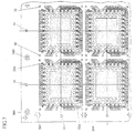
- Fig. 7 shows a conductive pattern formed on the conductive foil 20.
- four units are formed vertically, and horizontally eight units are formed so as to have a shape like lead frame.
- Symbols 30A and 30B are marks showing position of dicing line, and between two lines dicing blade is arranged so as to separate the semiconductor device individually.
- Symbols 31 and 32 are indexing marks.
- L shape lines shown with symbols 33A and 33B show corner portion of the chip. At the corner portion, the corner of the chip is arranged and fixed.
- the pad half-etched to make projection is formed on the conductive foil, it is possible to make the pad fine. Therefore it is possible to make width and gap of the pad narrow so as to form a small package in plan size.
- the device consists of necessary minimum components: the conductive pattern, the semiconductor chip, the connection means, and sealing material, useless material is removed so as to realize thin semiconductor device extremely depressing cost.
- tie bar and hanging lead are not need. Therefore forming and cutting tie bar (hanging lead) is not need at all in the invention.
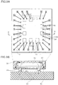
- Fig. 8 shows the semiconductor device 42.
- Fig. 8A is a plan view of the device, and
- Fig. 8B is a section view cut by A-A line.
- the pad 11A is formed in one body with the conductive path 11B and the external connection electrode 11C in Fig. 1, here the back face of the pad 11A becomes the external connection electrode.
- the pattern exposing from the insulating film 16 is formed in same pattern as said rectangle.
- the trenches 43 are formed so that the electrode 11D for radiation and chip 12 can be adhered appropriately by filling the insulating adhesion means into said trenches. Thereby the electrode 11D for radiation is divided to plural.
- the conductive foil (or conductive foil) where the conductive pattern formed in island shape has thickness is buried in the insulating adhesion means and the insulating resin.
- the electrode for radiation positioning at the back face of the semiconductor chip it is possible to improve radiation of the semiconductor chip.
- the supporting board is not used, it is possible to realize a thin and light package.
- the device consists of necessary minimum components of the conductive pattern, the semiconductor chip, and the insulating resin, and becomes a circuit device useless for resources. Therefore extra components do not exist till completion, and a semiconductor device decreasing cost thereof extremely.
Abstract

Description
- The present invention relates to a semiconductor device and a method for manufacturing the same, particularly a semiconductor device radiating excellently heat from the semiconductor device and a method for manufacturing the same.
- In recent years, use of IC package for portable equipment or small, hi-density mounting equipment progresses, and the conventional IC package and its concept of mounting are largely changing. These details are described in CSP technology, and mounting material and device supporting the technology - special issue of DENSHI ZAIRYO (p.22, Sep. 1998).
- Fig. 9 is a structure adopting a
flexible sheet 50 as an interposer board, acopper foil pattern 51 is put on the flexible sheet through adhesive, and an IC chip is fixed. There is a pad for bonding 53 formed at periphery of the IC chip as theconductive pattern 51. A pad for connectingsolder ball 54 is formed through aconductive path 51B formed in one body(integrally) with the pad for bonding 53. - At backside of the pad for connecting
solder ball 54, an opening 56 where the flexible sheet is opened, and through the opening 56, asolder ball 55 is formed. The entire body is sealed with aninsulating resin 58 using theflexible sheet 50 as a board.Symbol 57 is a bonding wire. - However the flexible sheet formed on a rear surface of IC chip is very expensive, and there are problems that cost rises, thickness of the package becomes thick, and weight increases.
- There is a problem that heat resistance from a back face of the IC chip to a back face of the package becomes large in a supporting board because the supporting board comprises material other than metal. For said supporting board, there is a flexible sheet, a ceramic board, or a printed board. A heat conduction path comprising material superior in heat conduction is the
bonding wire 57, thecopper foil 51, and thesolder ball 55, the above supporting board has a structure not to radiate fully at driving. Therefore there is a problem that driving current does not flow fully because of temperature rise of IC chip at driving. - The invention is carried out in view of the above problems , and intends to obtain a reliable semiconductor device having a small package and a good radiation characteristics.
- First, the problems are solved having a pad provided facing to a bonding electrode of a semiconductor chip, an electrode for radiation provided at an arranged area of said semiconductor chip, a insulating adhesion means provided on said electrode for radiation, said semiconductor chip fixed to said insulating adhesion means and electrically connected to said pad, and a insulating resin sealing(molding) said semiconductor chip so as to expose a back face of said pad and said insulating adhesion means and to make in one body.
- Second, the problem is solved by that said insulating adhesion means comprises an adhesion sheet or adhesive.
- Third, the problem is solved by that said semiconductor element is mounted in face-up type and that said pad and said bonding electrode are connected with fine metal wires (bonding wires).
- Fourth, the problem is solved by providing: plural bonding pads provided so as to surround one area; external connection electrodes extended in one body with said bonding pads; an electrode for radiation provided at said one area; a insulating adhesion means provided at said electrode for radiation; a semiconductor chip fixed through said insulating adhesion means; bonding wires connecting said bonding electrodes and said bonding pads on said semiconductor chip; and a insulating resin covering said semiconductor chip, said bonding pads, said electrode for radiation, said external connection electrodes, and said bonding wires and exposing back faces of said external connection electrodes, back faces of said electrodes for radiation, and back faces of said insulating adhesion means.
- Fifth, the problem is solved by providing: plural pads provided so as to surround one area; an electrode for radiation provided at said one area; a insulating adhesion means provided at said electrode for radiation; a semiconductor chip fixed through said insulating adhesion means; connecting means connecting said bonding electrodes and said pads on said semiconductor chip; and a insulating resin covering said semiconductor chip, said bonding pads, and said connection means, and exposing back faces of said bonding pads and said insulating adhesion means; wherein the back face of said bonding pads are used as the external connection electrode.
- Sixth, the problem is solved by that said connection means comprises a bonding wire or brazing material.
- Seventh, the problem is solved by that a side face of said pad, bonding pad, or external connection electrode comprises a curved structure.
- Eighth, the problem is solved by preparing a conductive foil and half-etching so that a conductive pattern is formed in projection shape;
- providing an insulating adhesion means so as to fill in an isolation trench formed by said half-etching;
- fixing a semiconductor chip through said insulating adhesion means so as to connect said conductive pattern electrically and;
- providing a insulating resin at said conductive foil so as to seal said semiconductor chip and said conductive pattern; and
- removing a back face of said conductive foil so as to exposing a back face of said insulating adhesion means and to separate as said conductive pattern.
-
- Ninth, the problem is solved by preparing a conductive foil and half-etching so that a conductive pattern comprising at least a pad and an electrode for radiation is formed in projection shape;
- forming an insulating adhesion means so as to cover said electrode for radiation and fill in an isolation trench adjacent to the electrode;
- fixing a semiconductor chip through said insulating adhesion means so as to connect said conductive pattern electrically and;
- providing a insulating resin at said conductive foil so as to seal said semiconductor chip and said conductive pad; and
- removing a back face of said conductive foil so as to exposing a back face of said insulating adhesion means and to separate said conductive pattern.
-
- By providing the semiconductor device, it is possible to transfer heat of a semiconductor chip to an electrode for radiation. As a conductive pattern including the electrode for radiation is formed without using a supporting board, it is possible to decrease cost and to make thickness of the semiconductor device thin.
- Fig. 1 is a view describing the semiconductor device of the invention.
- Fig. 2 is a view describing the method for manufacturing the semiconductor device of the invention.
- Fig. 3 is a view describing the method for manufacturing the semiconductor device of the invention.
- Fig. 4 is a view describing the method for manufacturing the semiconductor device of the invention.
- Fig. 5 is a view describing the method for manufacturing the semiconductor device of the invention.
- Fig. 6 is a view describing the method for manufacturing the semiconductor device of the invention.
- Fig. 7 is a view describing the conductive pattern used for the semiconductor device of the invention.
- Fig. 8 is a view describing the semiconductor device of the invention.
- Fig. 9 is a view describing the conventional semiconductor device.
- First mode for carrying out describing a semiconductor device
- First, a semiconductor device of the invention is described referring F1g. 1. Fig. 1A is a plan view of the semiconductor device, and Fig. 1B is a section view cut with A-A line.
- Fig. 1 shows a
insulating resin 10 buried with the following chips. They arepads 11A,conductive paths 11B in one body with the pads11A,external connection electrodes 11C provided at the other ends of theconductive paths 11B in one body with theconductive paths 11B. Further an electrode for radiating 11D provided at one area surrounded by theconductive patterns semiconductor chip 12 provided on the electrode for radiating 11D are buried. Thesemiconductor chip 12 is fixed to the electrode for radiating 11D through a insulating adhesion means AD, and is shown with dotted line in Fig. 1A. - A
bonding electrode 13 of thesemiconductor chip 12 and thepad 11A are electrically connected through abonding wire 14. - Side face of said
conductive pattern 11A to 11D is etched with non-anisotropy, and has a curved structure because of being formed with wet etching so as to generate anchor effect by the curved structure. - The structure consists of four materials: the
semiconductor chip 12, pluralconductive patterns 11A to 11C, the electrode forradiation 11D, the insulating adhesion means AD, and the insulatingresin 10 burying them. In arranged area of thesemiconductor chip 12, said insulating adhesion means AD is formed on and between theconductive patterns 11A to 11D, particularly is provided in theisolation trench 15 formed by etching so as to expose the back face. The insulatingresin 10 seals all including these materials.Said pads 11A andsemiconductor chip 12 are supported by the insulatingresin 10. - For the insulating adhesion means, adhesive comprising insulating material and insulating sheet of adhesiveness are desirable. As clear in the description below, material is desirable to bond entire wafer and to pattern by photolithography. For the insulating resin, thermosetting resin such as epoxy resin and thermoplastic resin such as polyimide resin and polyphenylenesulfide are used. All kinds of resin are used if they are resins hardening using a die and covering by dipping and painting. For the
conductive patterns 11A to 11D, conductive foil of Cu as main material, conductive foil of A1 as main material, Fe-Ni alloy, laminated product of Cu-Al, or laminated product of Al-Cu-Al is used. Of course, even other material is possible to use, particularly conductive material easy to etch and easy to evaporate by laser is desirable. Considering half-etching ability, forming ability of plating, and thermal stress, conductive material of Cu as main material formed by rolling is desirable. - The invention has a characteristic to prevent remove of the conductive pattern because the insulating
resin 10 and the insulating adhesion means AD are filled into even saidisolation trench 15. By carrying out non-anisotropic etching using dry etching or wet etching for etching, the side faces ofpads 11A are made into curved structure so as to generate anchor effect. As the result, the structure that theconductive patterns 11A to 11D do not come out (remove) from the insulating resin 10(package) is realized. - Further the back faces of the
conductive patterns 11A to 11D expose at the back face of the package. Accordingly the back face of theelectrode 11D for radiation is fixed with the electrode on the mounting board. The structure can radiate heat generating from thesemiconductor chip 12 on the electrode of the mounting board, can prevent temperature rise of thesemiconductor chip 12, and can increase driving current of thesemiconductor chip 12. The electrode forradiation 11C and thesemiconductor chip 12 may be connected electrically. - Because the
conductive patterns 11A to 11D are supported by insulatingresin 10 in the semiconductor device, a supporting board is not need. This construction is a characteristic of the invention. As described at the prior art, the conductive path of the conventional semiconductor device is supported by a supporting board (flexible sheet, printed board, or ceramic board), or supported by a lead frame, the construction which is not need originally is added. However the circuit device consists of necessary minimum components and does not need the supporting board so that the device has a characteristic to be thin, light, and inexpensive because of low material cost. - At the back face of the package, the
conductive patterns 11A to 11D expose. By covering brazing material such as solder for example, at the area, the brazing material can get wet thickly because area of the electrode forradiation 11D is broad. Therefore brazing material of the back face of theexternal connection electrode 11C is not wet at the electrode of the mounting board at fixing on the mounting board, so it is assumed to become bad connection. - To solve that, a insulating
film 16 is formed at the back face of thesemiconductor device 15. Circles of dotted line shown Fig. 1A show theexternal connection electrodes 11C and electrodes forradiation 11D exposing from the insulatingfilm 16. That is, as the insulatingfilm 16 covers portions except the circles and size of circle portions is substantially same size, thickness of brazing material formed here is substantially same. This is similar as after solder printing and after reflow. This is similar about conductive paste such as Ag, Au, Ag-Au, Ag-Pd and so on. By the structure, bad quality of the electrical connection means 23 are depressed. An exposingportion 17 of the electrode forradiation 11D may be formed larger than exposing size of theexternal connection electrode 11C considering radiation of the semiconductor chip. As all of theexternal connection electrodes 11C are substantially same size, all area of theexternal connection electrodes 11C may be exposed at entire area, and a part of the back face of the electrode forradiation 11D may be exposed from the insulatingfilm 16 with substantially same size. - By providing the insulating
film 16, it is possible to extend the conductive path provided at the mounting board to the back face of the semiconductor device. Although the conductive path provided at the mounting board side is generally arranged going around the fixed area of said semiconductor device, forming said insulatingfilm 16 can arrange without going around. Further as the insulatingresin 10 and the insulating adhesion means AD project from the conductive pattern, a gap is formed between the conductive path of the mounting board side and the conductive pattern so as to prevent short. - Second mode for carrying out describing a method for manufacturing a semiconductor device
- The method for manufacturing shows the method for manufacturing of the
semiconductor chip 15 shown in Fig. 1, and Fig. 2 to Fig. 6 are section views corresponding to A-A line of Fig. 1A. - First, a
conductive foil 20 is provided as Fig. 2. Thickness thereof is desirably 10 µm to 300 µm, here rolled copper foil of 70 µm is used. Next on the front face of theconductive foil 20, aconductive film 21 or a photo resist is formed as etching-resist. - The pattern is same pattern as the
pads 11A in Fig.1A, theconductive paths 11B, theexternal connection electrode 11C, and the electrodes forradiation 11D. In the case of using the photo resist instead of theconductive film 21, a conductive film such as Au, Ag, Pd or Ni is formed at a part corresponding to at least pad in the lower layer of the photo resist. This is provided to make bonding possible. (Refer Fig. 2 about the above.) - Next, a
conductive foil 20 is half-etched through saidconductive film 21 or photo resist. Depth of etching may be thinner than thickness ofconductive foil 20. The thinner the depth of etching, forming the finer pattern is possible. - By half-etching,
conductive patterns 11A to 11D appear at surface of theconductive foil 20 in projection shape. As above-mentioned, here Cu foil formed by roll and made of Cu as main material is used for theconductive foil 20. For the conductive foil, conductive foil made of AL, conductive foil made of Fe-Ni alloy, layered product of Cu-AL, or layered product of Al-Cu-Al may be used. Especially the layered product of Al-Cu-Al prevents bend appearing by difference of coefficient of thermal expansion. - At part corresponding to dotted line of Fig. 1, a insulating adhesion means AD is formed. The insulating adhesion means AD is provided at an
isolation trench 15 between the electrode ofradiation 11D and theexternal connection electrode 11C, at anisolation trench 15 between the electrode ofradiation 11D and theconductive path 11B, and on them. - Next, a
semiconductor chip 12 is fixed at one area providing the insulating adhesion means AD, abonding electrode 13 of thesemiconductor chip 12 and thebonding pad 11A are electrically connected. In the figure, as thesemiconductor chip 12 is mounted in face up type, abonding wire 14 is used for the connection means. - In the bonding, the
bonding pads 11A are in one body with theconductive foil 20, and further a back face of theconductive foil 20 contacts face of table of a bonding machine because the back face is flat. Therefore if theconductive foil 20 is entirely fixed to the bonding table, there is not position shift of thebonding pads 11A, and bonding energy is transferred efficiently to thebonding wire 14 and thebonding pads 11A. Therefore thebonding wire 14 is connected improving fixing strength thereof. Fixing the bonding table is possible by providing plural vacuum suction holes at entire face of the table for example. Theconductive foil 21 may be pushed from upper side. - The semiconductor chip is mounted without using the supporting board, and height of the
semiconductor chip 12 is arranged low as thickness as the supporting board. Therefore it is possible that thickness of the package is made thin. - A insulating
resin 10 is formed so as to cover theconductive patterns 11A to 11D formed by half-etched, thesemiconductor chip 12, and thebonding wire 14. For the insulating resin, both of thermoplasticity and thermosetting property may be used. - Transfer molding, injection molding, dipping, or painting realizes the resin. For the resin material, thermosetting resin such as epoxy resin is realized by transfer molding and thermoplastic resin such as liquid polymer and polyphenylenesulfide is realized by injection molding.
- In the mode for carrying out, thickness of the insulating resin is adjusted so as to cover 100 µm upper from an upper limit face of the
bonding wire 14. The thickness may be made thick or thin considering strength of the semiconductor device. - In the injection of resin, as the
conductive patterns 11A to 11D are in one body with the sheet-shapeconductive foil 20, position of theconductive patterns 11A to 11D does not shift at all as long as theconductive foil 20 does not shift. - As above-mentioned, in the insulating
resin 10, theconductive patterns 11A to 11D formed as projection and thesemiconductor chip 12 are buried, and theconductive foil 20 of lower part than the projection exposes at the back face. - Next, the
conductive foil 20 exposing at the back face of the insulatingresin 10 is removed and theconductive patterns 11A to 11D are individually separated. - Various methods are considered for the separating process, that is, the back face may be separated removing by etching or grinding by polishing or grinding. Both of them may be used. There is a problem that shavings of the
conductive foil 20 and bur-shape rolled metal extended thin to outside cut into the insulatingresin 10 and the insulating adhesion means AD at grinding till the insulatingresin 10 exposes for example. Therefore separating the conductive pattern by etching, the device is formed without that metal of theconductive foil 20 cuts into the insulatingresin 10 existing between theconductive pattern 11A to 11D and the insulating adhesion means AD. Thus short between theconductive pattern 11A to 11D of fine interval is prevented. (Refer Fig. 5 about the above.) - In the case that plural units becoming the
semiconductor device 15 are formed, dicing process is added after the separating process. - Although the units are separated individually using the dicing machine here, it is possible by chocolate breaking, pressing, and cutting.
- Here the insulating
film 16 is formed on theconductive patterns 11A to 11D exposing at the back face separated and is patterned so as to exposes the parts shown in circle of dotted line of Fig. 1A, and after that, is diced along an arrow shown in Fig 6 to be each of the semiconductor devices. - The
solder 21 may be formed before or after dicing. - The above method for manufacturing realizes a light, thin, short, small package where a semiconductor chip buried in insulating material.
- The insulating adhesion means AD shown in Fig. 3 and Fig. 4 may be bonded at the stage of wafer before the
semiconductor 12 is individually separated. Thatis, if sheet-shaped adhesive is formed on the back face of wafer at the stage wafer and the wafer is cut with the sheet at dicing, the process forming the insulating adhesion means AD on theconductive foil 20, shown in Fig. 3, is not need. - Fig. 7 shows a conductive pattern formed on the
conductive foil 20. Here four units are formed vertically, and horizontally eight units are formed so as to have a shape like lead frame. -
Symbols Symbols symbols - Next, effect generating by the above method for manufacturing is described.
- First, as the conductive pattern is half-etched and supported in one body of the conductive foil, a board used for supporting past is removed.
- Second, as the pad half-etched to make projection is formed on the conductive foil, it is possible to make the pad fine. Therefore it is possible to make width and gap of the pad narrow so as to form a small package in plan size.
- Third, as the device consists of necessary minimum components: the conductive pattern, the semiconductor chip, the connection means, and sealing material, useless material is removed so as to realize thin semiconductor device extremely depressing cost.
- Fourth, as the pads are formed becoming projection by half-etching and individually separated after sealing, tie bar and hanging lead are not need. Therefore forming and cutting tie bar (hanging lead) is not need at all in the invention.
- Fifth, as the conductive foil is removed from the back face of the insulating resin after the conductive pattern becoming the projection is buried in the insulating resin and is separated, bur of resin generating between leads as the conventional lead framed is removed.
- Sixth, as the semiconductor is fixed to the electrode for radiation through the insulating adhesive means and the electrode for radiation exposes from the back face thereof, heat generating from the semiconductor device is efficiently radiated from the back face thereof. By mixing the under-fill material with filler such as Si oxide film and aluminum oxide, radiation of the device is more improved. By unifying the filler size, it is possible that gap between the
semiconductor chip 12 and the conductive pattern is kept uniform. - Third mode for carrying out describing a semiconductor device
- Fig. 8 shows the semiconductor device 42. Fig. 8A is a plan view of the device, and Fig. 8B is a section view cut by A-A line.
- Although the
pad 11A is formed in one body with theconductive path 11B and theexternal connection electrode 11C in Fig. 1, here the back face of thepad 11A becomes the external connection electrode. - As the back face of the
pad 11A is formed in rectangle, the pattern exposing from the insulatingfilm 16 is formed in same pattern as said rectangle. Thetrenches 43 are formed so that theelectrode 11D for radiation andchip 12 can be adhered appropriately by filling the insulating adhesion means into said trenches. Thereby theelectrode 11D for radiation is divided to plural. - As clear from the above description, in the invention, even the conductive foil (or conductive foil) where the conductive pattern formed in island shape has thickness is buried in the insulating adhesion means and the insulating resin. As the electrode for radiation positioning at the back face of the semiconductor chip, it is possible to improve radiation of the semiconductor chip. Further as the supporting board is not used, it is possible to realize a thin and light package.
- The device consists of necessary minimum components of the conductive pattern, the semiconductor chip, and the insulating resin, and becomes a circuit device useless for resources. Therefore extra components do not exist till completion, and a semiconductor device decreasing cost thereof extremely.
Claims (9)
- A semiconductor device, comprising:a pad provided facing to a bonding electrode of a semiconductor chip;an electrode for radiation provided at an arranged area of said semiconductor chip;a insulating adhesion means provided on said electrode for radiation, said semiconductor chip fixed to said insulating adhesion means and electrically connected to said pad; anda insulating resin sealing said semiconductor chip so as to expose a back face of said pad and said insulating adhesion means and to make in one body.
- A semiconductor device according to Claim 1, wherein said insulating adhesion means comprises an adhesion sheet or a adhesive.
- A semiconductor device according to Claim 1, wherein said semiconductor chip is mounted in face-up type and that said pad and said bonding electrode are connected with a bonding wire.
- A semiconductor device according to claim 1, comprising:the pad of plural bonding pads provided so as to surround one area;external connection electrodes extended in one body with said bonding pads;said electrode for radiation provided at said one area;said insulating adhesion means provided at said electrode for radiation;said semiconductor chip fixed through said insulating adhesion means;bonding wires connecting said bonding electrodes and said bonding pads on said semiconductor chip; andsaid insulating resin covering said semiconductor chip, said bonding pads, said electrode for radiation, said external connection electrodes, and said bonding wires, and exposing back faces of said external connection electrodes, back faces of said electrodes for radiation, and back faces of said insulating adhesion means.
- A semiconductor device according to claim 1, comprising:said pad of plural pads provided so as to surround one area;said electrode for radiation provided at said one area;said insulating adhesion means provided at said electrode for radiation;said semiconductor chip fixed through said insulating adhesion means;connecting means connecting said bonding electrodes and said pads on said semiconductor chip; andsaid insulating resin covering said semiconductor chip, said bonding pads , and said connection means, and exposing back faces of said bonding pads and said insulating adhesion means;wherein the back face of said bonding pads are used as the external connection electrode.
- A semiconductor device according to Claim 5, wherein said connection means comprises a bonding wire or brazing material.
- A semiconductor device according to Claim 1 , wherein side face of said pad, bonding pad, or external connection electrode comprises a curved structure.
- A method for manufacturing a semiconductor device comprising the steps of:preparing a conductive foil and half-etching so that a conductive pattern is formed in projection shape;providing a insulating adhesion means so as to fill in an isolation trench formed by said half-etching;fixing a semiconductor chip through said insulating adhesion means so as to connect to said conductive pattern electrically and;providing an insulating resin at said conductive foil so as to seal said semiconductor chip and said conductive pattern; andremoving a back face of said conductive foil so as to exposing a back face of said insulating adhesion means and to separate as said conductive pattern.
- A method for manufacturing a semiconductor device according to claim 8: whereinsaid pattern comprises at least a pad and an electrode for radiation;said fixing step comprises the step of bonding said semiconductor chip to said electrode for radiation through the insulating adhesion means so as to connect said semiconductor chip with said pad
Applications Claiming Priority (2)
| Application Number | Priority Date | Filing Date | Title |
|---|---|---|---|
| JP2000269467 | 2000-09-06 | ||
| JP2000269467 | 2000-09-06 |
Publications (2)
| Publication Number | Publication Date |
|---|---|
| EP1187203A2 true EP1187203A2 (en) | 2002-03-13 |
| EP1187203A3 EP1187203A3 (en) | 2004-04-14 |
Family
ID=18756068
Family Applications (1)
| Application Number | Title | Priority Date | Filing Date |
|---|---|---|---|
| EP20010302549 Withdrawn EP1187203A3 (en) | 2000-09-06 | 2001-03-20 | A semiconductor device and method of manufacturing the same |
Country Status (5)
| Country | Link |
|---|---|
| US (2) | US6462418B2 (en) |
| EP (1) | EP1187203A3 (en) |
| KR (1) | KR100407595B1 (en) |
| CN (1) | CN1265451C (en) |
| TW (1) | TW501382B (en) |
Families Citing this family (60)
| Publication number | Priority date | Publication date | Assignee | Title |
|---|---|---|---|---|
| JP3420153B2 (en) * | 2000-01-24 | 2003-06-23 | Necエレクトロニクス株式会社 | Semiconductor device and manufacturing method thereof |
| JP3883784B2 (en) * | 2000-05-24 | 2007-02-21 | 三洋電機株式会社 | Plate-shaped body and method for manufacturing semiconductor device |
| JP3609737B2 (en) * | 2001-03-22 | 2005-01-12 | 三洋電機株式会社 | Circuit device manufacturing method |
| TW538658B (en) * | 2001-08-27 | 2003-06-21 | Sanyo Electric Co | Manufacturing method for circuit device |
| DE10148120B4 (en) * | 2001-09-28 | 2007-02-01 | Infineon Technologies Ag | Electronic components with semiconductor chips and a system carrier with component positions and method for producing a system carrier |
| CN1303852C (en) * | 2002-06-12 | 2007-03-07 | 威盛电子股份有限公司 | Radiating structure of lead frame package and method for improving radiating performance of the same package |
| JP2004179253A (en) * | 2002-11-25 | 2004-06-24 | Nec Semiconductors Kyushu Ltd | Semiconductor device and manufacturing method therefor |
| JP2004186362A (en) * | 2002-12-03 | 2004-07-02 | Sanyo Electric Co Ltd | Circuit device |
| SG119185A1 (en) | 2003-05-06 | 2006-02-28 | Micron Technology Inc | Method for packaging circuits and packaged circuits |
| JP2005109225A (en) * | 2003-09-30 | 2005-04-21 | Sanyo Electric Co Ltd | Circuit device |
| US7488565B2 (en) * | 2003-10-01 | 2009-02-10 | Chevron U.S.A. Inc. | Photoresist compositions comprising diamondoid derivatives |
| JP4446772B2 (en) * | 2004-03-24 | 2010-04-07 | 三洋電機株式会社 | Circuit device and manufacturing method thereof |
| JP4489485B2 (en) | 2004-03-31 | 2010-06-23 | 株式会社ルネサステクノロジ | Semiconductor device |
| WO2006132151A1 (en) * | 2005-06-06 | 2006-12-14 | Rohm Co., Ltd. | Interposer and semiconductor device |
| JP5081578B2 (en) | 2007-10-25 | 2012-11-28 | ローム株式会社 | Resin-sealed semiconductor device |
| US7727813B2 (en) * | 2007-11-26 | 2010-06-01 | Infineon Technologies Ag | Method for making a device including placing a semiconductor chip on a substrate |
| US9536815B2 (en) | 2009-05-28 | 2017-01-03 | Hsio Technologies, Llc | Semiconductor socket with direct selective metalization |
| WO2010147939A1 (en) | 2009-06-17 | 2010-12-23 | Hsio Technologies, Llc | Semiconductor socket |
| WO2010138493A1 (en) | 2009-05-28 | 2010-12-02 | Hsio Technologies, Llc | High performance surface mount electrical interconnect |
| US9276336B2 (en) | 2009-05-28 | 2016-03-01 | Hsio Technologies, Llc | Metalized pad to electrical contact interface |
| WO2011153298A1 (en) | 2010-06-03 | 2011-12-08 | Hsio Technologies, Llc | Electrical connector insulator housing |
| WO2010147934A1 (en) * | 2009-06-16 | 2010-12-23 | Hsio Technologies, Llc | Semiconductor die terminal |
| US8987886B2 (en) | 2009-06-02 | 2015-03-24 | Hsio Technologies, Llc | Copper pillar full metal via electrical circuit structure |
| US9136196B2 (en) | 2009-06-02 | 2015-09-15 | Hsio Technologies, Llc | Compliant printed circuit wafer level semiconductor package |
| US9276339B2 (en) | 2009-06-02 | 2016-03-01 | Hsio Technologies, Llc | Electrical interconnect IC device socket |
| US9184145B2 (en) | 2009-06-02 | 2015-11-10 | Hsio Technologies, Llc | Semiconductor device package adapter |
| WO2010141296A1 (en) | 2009-06-02 | 2010-12-09 | Hsio Technologies, Llc | Compliant printed circuit semiconductor package |
| US9930775B2 (en) | 2009-06-02 | 2018-03-27 | Hsio Technologies, Llc | Copper pillar full metal via electrical circuit structure |
| WO2010141264A1 (en) | 2009-06-03 | 2010-12-09 | Hsio Technologies, Llc | Compliant wafer level probe assembly |
| US8928344B2 (en) | 2009-06-02 | 2015-01-06 | Hsio Technologies, Llc | Compliant printed circuit socket diagnostic tool |
| WO2010141316A1 (en) | 2009-06-02 | 2010-12-09 | Hsio Technologies, Llc | Compliant printed circuit wafer probe diagnostic tool |
| WO2010141298A1 (en) | 2009-06-02 | 2010-12-09 | Hsio Technologies, Llc | Composite polymer-metal electrical contacts |
| WO2011002712A1 (en) | 2009-06-29 | 2011-01-06 | Hsio Technologies, Llc | Singulated semiconductor device separable electrical interconnect |
| US8988093B2 (en) | 2009-06-02 | 2015-03-24 | Hsio Technologies, Llc | Bumped semiconductor wafer or die level electrical interconnect |
| WO2012078493A1 (en) | 2010-12-06 | 2012-06-14 | Hsio Technologies, Llc | Electrical interconnect ic device socket |
| US8525346B2 (en) | 2009-06-02 | 2013-09-03 | Hsio Technologies, Llc | Compliant conductive nano-particle electrical interconnect |
| WO2010141303A1 (en) | 2009-06-02 | 2010-12-09 | Hsio Technologies, Llc | Resilient conductive electrical interconnect |
| US8610265B2 (en) | 2009-06-02 | 2013-12-17 | Hsio Technologies, Llc | Compliant core peripheral lead semiconductor test socket |
| US9196980B2 (en) | 2009-06-02 | 2015-11-24 | Hsio Technologies, Llc | High performance surface mount electrical interconnect with external biased normal force loading |
| WO2014011226A1 (en) | 2012-07-10 | 2014-01-16 | Hsio Technologies, Llc | Hybrid printed circuit assembly with low density main core and embedded high density circuit regions |
| US9613841B2 (en) | 2009-06-02 | 2017-04-04 | Hsio Technologies, Llc | Area array semiconductor device package interconnect structure with optional package-to-package or flexible circuit to package connection |
| WO2013036565A1 (en) | 2011-09-08 | 2013-03-14 | Hsio Technologies, Llc | Direct metalization of electrical circuit structures |
| US9318862B2 (en) | 2009-06-02 | 2016-04-19 | Hsio Technologies, Llc | Method of making an electronic interconnect |
| US9232654B2 (en) | 2009-06-02 | 2016-01-05 | Hsio Technologies, Llc | High performance electrical circuit structure |
| US9093767B2 (en) | 2009-06-02 | 2015-07-28 | Hsio Technologies, Llc | High performance surface mount electrical interconnect |
| US8789272B2 (en) | 2009-06-02 | 2014-07-29 | Hsio Technologies, Llc | Method of making a compliant printed circuit peripheral lead semiconductor test socket |
| US9414500B2 (en) | 2009-06-02 | 2016-08-09 | Hsio Technologies, Llc | Compliant printed flexible circuit |
| WO2011002709A1 (en) | 2009-06-29 | 2011-01-06 | Hsio Technologies, Llc | Compliant printed circuit semiconductor tester interface |
| US8955216B2 (en) | 2009-06-02 | 2015-02-17 | Hsio Technologies, Llc | Method of making a compliant printed circuit peripheral lead semiconductor package |
| WO2010141311A1 (en) | 2009-06-02 | 2010-12-09 | Hsio Technologies, Llc | Compliant printed circuit area array semiconductor device package |
| US8981568B2 (en) | 2009-06-16 | 2015-03-17 | Hsio Technologies, Llc | Simulated wirebond semiconductor package |
| US10159154B2 (en) | 2010-06-03 | 2018-12-18 | Hsio Technologies, Llc | Fusion bonded liquid crystal polymer circuit structure |
| US9350093B2 (en) | 2010-06-03 | 2016-05-24 | Hsio Technologies, Llc | Selective metalization of electrical connector or socket housing |
| US8758067B2 (en) | 2010-06-03 | 2014-06-24 | Hsio Technologies, Llc | Selective metalization of electrical connector or socket housing |
| US9689897B2 (en) | 2010-06-03 | 2017-06-27 | Hsio Technologies, Llc | Performance enhanced semiconductor socket |
| US9761520B2 (en) | 2012-07-10 | 2017-09-12 | Hsio Technologies, Llc | Method of making an electrical connector having electrodeposited terminals |
| US10667410B2 (en) | 2013-07-11 | 2020-05-26 | Hsio Technologies, Llc | Method of making a fusion bonded circuit structure |
| US10506722B2 (en) | 2013-07-11 | 2019-12-10 | Hsio Technologies, Llc | Fusion bonded liquid crystal polymer electrical circuit structure |
| US9755335B2 (en) | 2015-03-18 | 2017-09-05 | Hsio Technologies, Llc | Low profile electrical interconnect with fusion bonded contact retention and solder wick reduction |
| KR101944783B1 (en) | 2017-01-16 | 2019-04-18 | 일진머티리얼즈 주식회사 | Copper foil attached to the carrier foil |
Citations (1)
| Publication number | Priority date | Publication date | Assignee | Title |
|---|---|---|---|---|
| US5976912A (en) * | 1994-03-18 | 1999-11-02 | Hitachi Chemical Company, Ltd. | Fabrication process of semiconductor package and semiconductor package |
Family Cites Families (7)
| Publication number | Priority date | Publication date | Assignee | Title |
|---|---|---|---|---|
| JP3509274B2 (en) * | 1994-07-13 | 2004-03-22 | セイコーエプソン株式会社 | Resin-sealed semiconductor device and method of manufacturing the same |
| US6001671A (en) * | 1996-04-18 | 1999-12-14 | Tessera, Inc. | Methods for manufacturing a semiconductor package having a sacrificial layer |
| JPH09312355A (en) * | 1996-05-21 | 1997-12-02 | Shinko Electric Ind Co Ltd | Semiconductor device and its manufacture |
| JPH10335566A (en) * | 1997-04-02 | 1998-12-18 | Dainippon Printing Co Ltd | Resin-sealed semiconductor device and circuit member used therein, and manufacture of resin-sealed semiconductor device |
| US6201292B1 (en) * | 1997-04-02 | 2001-03-13 | Dai Nippon Insatsu Kabushiki Kaisha | Resin-sealed semiconductor device, circuit member used therefor |
| JP3521758B2 (en) * | 1997-10-28 | 2004-04-19 | セイコーエプソン株式会社 | Method for manufacturing semiconductor device |
| JPH11195742A (en) * | 1998-01-05 | 1999-07-21 | Matsushita Electron Corp | Semiconductor device, manufacture thereof, and led frame therefor |
-
2001
- 2001-02-15 CN CNB011045531A patent/CN1265451C/en not_active Expired - Fee Related
- 2001-02-16 TW TW90103573A patent/TW501382B/en not_active IP Right Cessation
- 2001-02-24 KR KR10-2001-0009507A patent/KR100407595B1/en not_active IP Right Cessation
- 2001-03-16 US US09/809,849 patent/US6462418B2/en not_active Expired - Lifetime
- 2001-03-20 EP EP20010302549 patent/EP1187203A3/en not_active Withdrawn
-
2002
- 2002-09-06 US US10/236,502 patent/US6596564B2/en not_active Expired - Fee Related
Patent Citations (1)
| Publication number | Priority date | Publication date | Assignee | Title |
|---|---|---|---|---|
| US5976912A (en) * | 1994-03-18 | 1999-11-02 | Hitachi Chemical Company, Ltd. | Fabrication process of semiconductor package and semiconductor package |
Also Published As
| Publication number | Publication date |
|---|---|
| US20030011065A1 (en) | 2003-01-16 |
| KR100407595B1 (en) | 2003-12-01 |
| TW501382B (en) | 2002-09-01 |
| US6462418B2 (en) | 2002-10-08 |
| US6596564B2 (en) | 2003-07-22 |
| US20020027290A1 (en) | 2002-03-07 |
| CN1341962A (en) | 2002-03-27 |
| CN1265451C (en) | 2006-07-19 |
| EP1187203A3 (en) | 2004-04-14 |
| KR20020020169A (en) | 2002-03-14 |
Similar Documents
| Publication | Publication Date | Title |
|---|---|---|
| US6596564B2 (en) | Semiconductor device and method of manufacturing the same | |
| JP3650001B2 (en) | Semiconductor device and manufacturing method thereof | |
| EP1085561B1 (en) | Chip scale surface mount package for semiconductor device and process of fabricating the same | |
| US6909178B2 (en) | Semiconductor device and method of manufacturing the same | |
| JP3420057B2 (en) | Resin-sealed semiconductor device | |
| US7439097B2 (en) | Taped lead frames and methods of making and using the same in semiconductor packaging | |
| US6548328B1 (en) | Circuit device and manufacturing method of circuit device | |
| US7138296B2 (en) | Board for manufacturing a BGA and method of manufacturing semiconductor device using thereof | |
| US6791199B2 (en) | Heat radiating semiconductor device | |
| US6963126B2 (en) | Semiconductor device with under-fill material below a surface of a semiconductor chip | |
| JP3668101B2 (en) | Semiconductor device | |
| JP2001217372A (en) | Circuit device and method of manufacturing the same | |
| JP3510841B2 (en) | Plate, lead frame, and method of manufacturing semiconductor device | |
| JP3510839B2 (en) | Semiconductor device and manufacturing method thereof | |
| JP3963914B2 (en) | Semiconductor device | |
| JP3869633B2 (en) | Manufacturing method of semiconductor device | |
| JP3639495B2 (en) | Circuit device manufacturing method | |
| JP3778783B2 (en) | Circuit device and manufacturing method thereof | |
| JP4036603B2 (en) | Semiconductor device and manufacturing method thereof | |
| JP3691328B2 (en) | Circuit device and circuit module | |
| JP2002057173A (en) | Manufacturing method of circuit device | |
| JP2004039679A (en) | Circuit device | |
| JP2002026180A (en) | Method for manufacturing circuit device |
Legal Events
| Date | Code | Title | Description |
|---|---|---|---|
| PUAI | Public reference made under article 153(3) epc to a published international application that has entered the european phase |
Free format text: ORIGINAL CODE: 0009012 |
|
| AK | Designated contracting states |
Kind code of ref document: A2 Designated state(s): AT BE CH CY DE DK ES FI FR GB GR IE IT LI LU MC NL PT SE TR |
|
| AX | Request for extension of the european patent |
Free format text: AL;LT;LV;MK;RO;SI |
|
| PUAL | Search report despatched |
Free format text: ORIGINAL CODE: 0009013 |
|
| AK | Designated contracting states |
Kind code of ref document: A3 Designated state(s): AT BE CH CY DE DK ES FI FR GB GR IE IT LI LU MC NL PT SE TR |
|
| AX | Request for extension of the european patent |
Extension state: AL LT LV MK RO SI |
|
| RIC1 | Information provided on ipc code assigned before grant |
Ipc: 7H 01L 23/433 B Ipc: 7H 01L 21/48 B Ipc: 7H 01L 23/31 B Ipc: 7H 01L 23/495 A |
|
| 17P | Request for examination filed |
Effective date: 20040727 |
|
| AKX | Designation fees paid |
Designated state(s): DE FI FR GB NL |
|
| 17Q | First examination report despatched |
Effective date: 20061220 |
|
| STAA | Information on the status of an ep patent application or granted ep patent |
Free format text: STATUS: THE APPLICATION IS DEEMED TO BE WITHDRAWN |
|
| 18D | Application deemed to be withdrawn |
Effective date: 20070503 |