EP1202094A1 - Flexible optical circuit appliques - Google Patents
Flexible optical circuit appliques Download PDFInfo
- Publication number
- EP1202094A1 EP1202094A1 EP01129469A EP01129469A EP1202094A1 EP 1202094 A1 EP1202094 A1 EP 1202094A1 EP 01129469 A EP01129469 A EP 01129469A EP 01129469 A EP01129469 A EP 01129469A EP 1202094 A1 EP1202094 A1 EP 1202094A1
- Authority
- EP
- European Patent Office
- Prior art keywords
- adhesive
- backing layer
- optical fiber
- layer
- microstructures
- Prior art date
- Legal status (The legal status is an assumption and is not a legal conclusion. Google has not performed a legal analysis and makes no representation as to the accuracy of the status listed.)
- Withdrawn
Links
Images


Classifications
-
- G—PHYSICS
- G02—OPTICS
- G02B—OPTICAL ELEMENTS, SYSTEMS OR APPARATUS
- G02B6/00—Light guides; Structural details of arrangements comprising light guides and other optical elements, e.g. couplings
- G02B6/24—Coupling light guides
- G02B6/42—Coupling light guides with opto-electronic elements
- G02B6/43—Arrangements comprising a plurality of opto-electronic elements and associated optical interconnections
-
- G—PHYSICS
- G02—OPTICS
- G02B—OPTICAL ELEMENTS, SYSTEMS OR APPARATUS
- G02B6/00—Light guides; Structural details of arrangements comprising light guides and other optical elements, e.g. couplings
- G02B6/24—Coupling light guides
- G02B6/36—Mechanical coupling means
- G02B6/3608—Fibre wiring boards, i.e. where fibres are embedded or attached in a pattern on or to a substrate, e.g. flexible sheets
- G02B6/3612—Wiring methods or machines
-
- Y—GENERAL TAGGING OF NEW TECHNOLOGICAL DEVELOPMENTS; GENERAL TAGGING OF CROSS-SECTIONAL TECHNOLOGIES SPANNING OVER SEVERAL SECTIONS OF THE IPC; TECHNICAL SUBJECTS COVERED BY FORMER USPC CROSS-REFERENCE ART COLLECTIONS [XRACs] AND DIGESTS
- Y10—TECHNICAL SUBJECTS COVERED BY FORMER USPC
- Y10S—TECHNICAL SUBJECTS COVERED BY FORMER USPC CROSS-REFERENCE ART COLLECTIONS [XRACs] AND DIGESTS
- Y10S428/00—Stock material or miscellaneous articles
- Y10S428/914—Transfer or decalcomania
-
- Y—GENERAL TAGGING OF NEW TECHNOLOGICAL DEVELOPMENTS; GENERAL TAGGING OF CROSS-SECTIONAL TECHNOLOGIES SPANNING OVER SEVERAL SECTIONS OF THE IPC; TECHNICAL SUBJECTS COVERED BY FORMER USPC CROSS-REFERENCE ART COLLECTIONS [XRACs] AND DIGESTS
- Y10—TECHNICAL SUBJECTS COVERED BY FORMER USPC
- Y10T—TECHNICAL SUBJECTS COVERED BY FORMER US CLASSIFICATION
- Y10T428/00—Stock material or miscellaneous articles
- Y10T428/28—Web or sheet containing structurally defined element or component and having an adhesive outermost layer
- Y10T428/2813—Heat or solvent activated or sealable
- Y10T428/2817—Heat sealable
-
- Y—GENERAL TAGGING OF NEW TECHNOLOGICAL DEVELOPMENTS; GENERAL TAGGING OF CROSS-SECTIONAL TECHNOLOGIES SPANNING OVER SEVERAL SECTIONS OF THE IPC; TECHNICAL SUBJECTS COVERED BY FORMER USPC CROSS-REFERENCE ART COLLECTIONS [XRACs] AND DIGESTS
- Y10—TECHNICAL SUBJECTS COVERED BY FORMER USPC
- Y10T—TECHNICAL SUBJECTS COVERED BY FORMER US CLASSIFICATION
- Y10T428/00—Stock material or miscellaneous articles
- Y10T428/29—Coated or structually defined flake, particle, cell, strand, strand portion, rod, filament, macroscopic fiber or mass thereof
- Y10T428/2913—Rod, strand, filament or fiber
- Y10T428/2922—Nonlinear [e.g., crimped, coiled, etc.]
Definitions
- the present invention relates to flexible optical circuits.
- the present invention relates to flexible optical circuits having a backing layer, an adhesive coating and a release liner for attachment to a substrate such as an electronic printed circuit board.
- optical interconnects In an attempt to handle higher speeds, interconnection technology has turned to optical interconnects for next generation circuits. Optical circuits have bandwidth capabilities orders of magnitude beyond electrical circuits, and are inherently immune to electrical interference. In some known designs, discrete fiber optic cables and fiber bundles are used to interconnect devices. Known standard fiber optic connection technology employed to connect optical fibers to devices are adequate for small numbers of interconnections. However, as optical circuit density grows, the physical bulk of cables and connectors make this approach unwieldy, especially for compact designs.
- Flexible optical interconnect circuit packs are also known in the art. An example of this is found in U.S. Patent No. 5,204,925 to Bonanni, et al.
- the known optical interconnect circuits have optical fibers bonded between two flexible substrates and have one or more optical connectors connected along the edges of the circuit pack. The connectors are then connected to one or more optical devices. These known devices are not adapted to bond to a substrate or circuit board.
- One known solution to the above problem is to use a less aggressive adhesive so the user may remove or reposition the film in case of misalignment. This can result in poor long term adhesion.
- Another known solution is to use a partially cured adhesive material followed by a final curing process. This not only results in additional process step, but may be impractical for many applications.
- Yet another known solution is to prepare a surface wetted with a material that interferes with adhesion and then removing the wetting agent after final alignment is achieved. This approach can be messy and adds process steps.
- the present invention provides a flexible optical circuit applique that can be mounted on a circuit board without modifying the circuit board substrate or the electronic circuits.
- the optical circuit applique of the present invention is also repositionable.
- a method of manufacturing flexible optical circuit appliques is also provided.
- a preformed fiber optic applique having a backing layer.
- the backing layer or film has an adhesive coating applied thereon.
- At least one optical fiber is routed and bonded to the adhesive layer providing a continuous optical signal path from one end to another.
- a releasable liner is releasably attached to the adhesive layer and positioned to cover the backing layer including the at least one optical fiber.
- microstructures are provided on the backing layer.
- the microstructures are crushable structures that prevent the adhesive coating from immediately adhering to a substrate. This allows the film to be repositioned until proper alignment has been achieved. Upon the application of appropriate force, the microstructures will crush allowing the adhesive coating to bond the film to the substrate.
- a method of fabricating the fiber optic appliques of the present invention includes the steps of providing a supply of backing layer and applying an adhesive coating to the backing layer. At least one fiber is then provided and placed on the adhesive coating. Pressure is then applied to the at least one fiber to secure it to the backing layer.
- the present invention provides a flexible optical circuit applique having a flexible backing with fibers bonded thereto covered by a releasable liner.
- the optical appliques are intended to provide an easy means for adding optical circuits to electronic circuit boards or other substrates by laminating.
- the flexible optical circuits of the present invention can also be incorporated into new board designs without changing standard board design and fabrication techniques.
- the optical appliques of the present invention are also repositionable on a substrate prior to bonding.
- FIG 1 is a perspective view of a preferred embodiment of a flexible optical circuit applique 10 according to the present invention. Also illustrated is a printed circuit board 12 to which applique 10 is to be mounted. Applique 10 comprises a durable backing material 14 that is coated with a temporarily repositionable adhesive 16. Applique 10 also includes optical fibers 18 bonded to backing 14 via adhesive 16. The particular backing material used depends upon the particular application. For instance, if high durability is desired, a polyester-type backing would be used. If the applique is to be mounted on a curved substrate, a flexible backing material would be chosen. Examples of backing materials include vinyl, polyurethane, polyamide, and polyester.
- Adhesive 16 of the present invention is any temporarily repositionable adhesive.
- temporarily repositionable it is meant that the bond between the adhesive and the substrate is such that the material having the adhesive may be removed from the substrate without damaging either for a period of time or until the occurrence of a specified event which then permanently adheres the backing to the substrate.
- adhesive 16 is preferably a pressure sensitive adhesive.
- Pressure sensitive adhesives are known in the industry as a standard class of materials. They are adhesives, which in dry form (substantially solvent free except for residual solvent) are aggressively and permanently tacky at room temperature (approximately 15° to 25° C) and firmly adhere to a variety of similar surfaces upon mere contact without the need for more than manual pressure.
- the adhesives require no activation by water, solvent, or heat in order to exert a strong adhesive holding force towards such materials as paper, cellophane, glass, plastic, wood, and metals.
- the adhesives have a sufficiently cohesive holding and elastic nature such that, despite their aggressive tackiness, it can be handled with fingers and removed from smooth surfaces without leaving a substantial residue.
- U.S. Patent Nos. 5,296,277, 5,362,516 and 5,449,540 which are assigned to the Assignee of the present invention.
- a release liner may not be required to cover the adhesive layer, and the backing material 14 may act as a release liner when the film is rolled.
- a light cured adhesive could be used with a transparent backing layer without departing from the spirit or scope of the invention. Such an adhesive would allow the film to be repositioned on a substrate until a light source, typically an ultra violet light, is applied through the transparent film which would then activate the adhesive to secure the film to the substrate.
- a light source typically an ultra violet light
- Nonpressure sensitive adhesives, thermally activated adhesives such as hot melt glue or solvent activated adhesives could also be used if desired, without departing from the spirit or scope of the invention. They are, however, less preferred embodiments because of the additional application steps and greater tendency to entrap air during application.
- Optical fibers 18 of the present invention are preferably 80 to 100 micron glass (silica) diameter fibers with a special fiber coating described in U.S. Patent No. 5,381,504.
- Standard glass optical fibers have 125 micron outside diameters.
- the present invention can obtain bend radiuses as small as 0.25 inches (0.64 cm) while staying below a bending stress of 100 K psi.
- a fiber having a diameter of 125 microns has a bending stress of approximately 110 K psi and a fiber having a diameter of 200 microns has a bending stress of approximately 175 K psi.
- bend radii of less than 0.3 inches (0.76 cm) are achieved at bend stresses of less than 100 K psi.
- FIG. 2a illustrates a preferred method of fabricating an applique according to the present invention.
- a supply roll 20 of applique backing layer or film, 14 is provided, as is a takeup roll 22.
- Film 14 is precoated with an adhesive layer 16 and covered with a releasable liner 17.
- a second takeup roller 19 is provided to take away releasable liner 17 as illustrated.
- a rotating drum 24 is provided to move backing film 14 from supply roll 20 to takeup roll 22.
- Multiple spools 28 of fibers 18 are provided and are suspended above backing film 14.
- a laminating roll spacing guide 30 is provided to space fibers 18 as desired and to press the fibers onto backing film 14 with sufficient force to activate pressure sensitive adhesive 16 to bond fibers 18 in place.
- a second supply roller 32 is provided carrying a second releasable liner 34 which releasably adheres to pressure sensitive adhesive 16.
- film 14 may be a continuous and solid film or it may have holes formed therethrough for connectorization with optical circuit components, as will be described in greater detail below.
- Figure 2b illustrates an alternative method of fabricating an applique according to the present invention.
- Figure 2b is similar to Figure 2a and thus like elements are correspondingly identified.
- Supply roll 20 of applique backing film 14 is provided as is takeup roll 22.
- Rotating drum 24 is provided to move backing film 14 from supply roll 20 to takeup roll 22.
- a pressure sensitive adhesive coating device 26 is provided to apply a coating of pressure sensitive adhesive 16 to backing film 14 as the backing film comes off of supply roll 20.
- Multiple spools 28 of fibers 18 are provided and are suspended above backing film 14.
- Laminating roll spacing guide 30 is provided to space fibers 18 as desired and to press the fibers onto backing film 14 with sufficient force to activate pressure sensitive adhesive 16 to bond fibers 18 in place.
- Second supply roller 32 is provided carrying release liner 34 which releasably adheres to pressure sensitive adhesive 16.
- Fabricating appliques in a continuous web process is a very cost effective way to fabricate the appliques.
- large numbers of standard appliques can easily be made from a single roll of backing film 14.
- Figures 3a - 3d illustrate alternative ways to make fibers 18 available for connectorization in a continuous web process similar to those described in Figures 2a and 2b above. It should be noted that the examples given below are given only as exemplary ways to avail the fibers for connectorization, and the examples given are not meant to be an exhaustive list. The illustrations in Figures 3a-3d use some of the same components as used in Figures 1 and 2, therefore, like elements will be correspondingly identified.
- film 14 is coated with adhesive layer 16. Fibers 18 are bonded to adhesive layer 16 as previously described.
- a release strip 35 is provided across the width of film 14 at predetermined intervals. The web is then cut at release strips 35.
- release strips 35 When applied to a substrate, release strips 35 prevent the ends of the individual applique section from adhering to the substrate thus allowing the ends of the fibers to be prepared for connectorization. It should be noted that release strip 35 not need to extend across the entire width of film 14.
- a series of receiving cavities 37 are formed through film 14. The receiving cavities allow access to fibers 18 when the applique is adhered to a substrate.
- Figure 3c illustrates a series of mechanical alignment devices 39 spaced at desired locations along the continuous web.
- Alignment devices 39 provide mechanical alignment for fibers 18 and also function as release liners.
- Mechanical alignment devices 39 are preferably V grooved structures, but may also be U shaped or other shapes that provide adequate alignment for fibers 18.
- Alignment device 39 may be removed prior to adhering to a substrate.
- Alignment device 39 could also be left in place with the applique adhered to a substrate.
- a connector assembly is then mounted around the fibers.
- an adhesiveless area 41 is provided on film 14. Thus, when film 14 is adhered to substrate, fibers 18 are not adhered to the substrate in adhesiveless area 41.
- the design of the applique according to the present invention including the number of fibers, the spacing of the fibers as well as the routing patterns can be done during the manufacturing process using a simple process control computer software program. Therefore, a board designer may layout a board and provide the manufacturer of the appliques of the present invention a layout of the board and an applique may be quickly and easily laid out by the process control program. Design and manufacture of appliques of the present invention may be conducted by, for example, Icon Industries, Euless, TX.
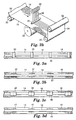
- Figures 4a, b and c illustrate some standard applique constructions.
- Figure 4a illustrates a 180° bend applique 36.
- Figure 4b illustrates a 90° bend applique 38 and
- Figure 4c illustrates a straight applique 40.
- Additional standard applique constructions besides the ones illustrated in Figures 4a-c, such as 30° bends, 60° bends, 45° bends etc., are also considered within the spirit and scope of the present invention.
- a continuous web construction having alternating patterns may be formed.
- Standard appliques such as those discussed above can be premade and purchased ready to use. Because the appliques of Figures 4a-c may be purchased as ready to use appliques, the ends of fibers 18 are also prepared for connectorization.
- Appliques 10 can be applied to circuit boards 12 or other substrates by users during the manufacturing process, by removing release liners 34 (not shown in Figures 4a, 4b or 4c) from the adhesive surface and laminating the applique to the circuit board surface. It should be noted that multiple appliques can be placed over one another without degrading performance.
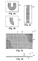
- FIGS 5a and b illustrate top and side plan views of flexible optical circuit applique 10 incorporating microreplicated structures 42 formed on backing film 14 or in adhesive surface 16.
- Microreplicated structures 42 are provided to allow accurate positioning of applique 10. Improper placement or accidental contact of an active adhesive surface can contribute to misalignment and immediate bonding to the desired surface. Because the microstructures protrude up from backing film 14 and are taller than the depth of adhesive coating 16, microstructures 42 prevent intimate contact between adhesive surface 16 and circuit board 12 or other mounting surface. Structures 42 are crushable such that intimate contact between adhesive surface 16 and circuit board 12 is obtained when suitable pressure is applied. Thus, the present invention may be repositioned until accurate alignment is achieved and further provides a high final bond strength after lamination.
- microreplicated structures of the present invention are preferably approximately 15 micrometers high. Additionally, the density or durometer of structures 42 can be varied to provide lesser or greater resistance to crushing or forming. For a more detailed description of microstructures 42, reference should be made to the above mentioned U.S. Patent Nos. 5,296,277, 5,362,516 and 5,449,540. It should be noted that alternative embodiments of microstructures 42 or other repositionable adhesive constructions are also considered within the spirit and scope of the present invention.
- the adhesive may contain microspheres which may house a catalyst, either with or without the presence of microstructures 42, such that when sufficient force is applied, the microspheres, and microstructures if present, are crushed and the catalyst is released, reacting with adhesive 16 to form an aggressive adhesive.
- Figures 6a and b illustrate an applique having microstructures 42 arranged in desired patterns such that microreplicated structures 42 provide a guide for routing fibers 18 in precise locations when bonded to adhesive surface 16. As illustrated in Figures 6a and 6b, fibers 18 fit into channels 44 between structures 42 and may thus be bonded to adhesive surface 16 without crushing structures 42. As previously stated, the microstructures may be positioned as described to form any such pattern.
- Microstructures 42 may be formed on backing film 14 before applying adhesive coating 16. Or, they may be added to adhesive surface 16 after applique 10 is constructed and fibers 18 are bonded to film 14 by having microstructures 42 picked up from an embossed release liner 34 which is attached immediately after fabrication.
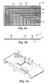
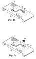
- Figures 7a-d illustrate steps for fabricating an applique according to the present invention that terminates fibers 18 in sockets or connectors.
- a multichip module positioning fixture 52 is provided to give support to backing film 14 and to provide a pattern for cutting out receiving cavities where sockets are inserted.
- Backing film 14 is unspooled and placed over positioning fixture 52 as illustrated in Figure 7a.
- Pressure sensitive adhesive 16 is either applied to backing film 14 or backing film 14 already has an adhesive layer coating thereon.
- Optical fibers 18 are then routed to desired positions on backing film 14. The paths taken by fibers 18 may follow parallel or individual routes, and provide a continuous signal path from one end to another. The optical circuit paths may also cross previously installed fibers producing multiple layers to optimize path geometry.
- fibers 18 are routed appropriately, they are bonded to backing film 14 by applying sufficient force to activate pressure sensitive adhesive 16. At this point, backing film 14 is cut at positions 49 where sockets are to be installed. As shown in Fig. 7b, the ends of fibers 18 are then cut, cleaved, sawed, polished or otherwise prepared for termination depending on user requirements. For ease of connectorization, optical fibers 18 are usually terminated in connectors or sockets 50. After preparing fiber ends, socket 50 is inserted through the hole formed in backing film 14 (Fig. 7c). Finally, as shown in Fig. 7d, a circuit board or other substrate 12 is bonded to backing film 14 and the backing film is cut to fit in the circuit board.
- the appliques of the present invention allow the optical paths formed by fibers 18 to be pretested before applying to circuit board 12 or any other substrate. Another benefit of the present invention is that fibers 18 are protected by film 14 when applied to circuit board 12. As previously stated, the backing film may vary depending upon the application. If greater protection for fibers 18 is needed, a stronger or thicker backing may be chosen. A further benefit of the appliques of the present invention is that the risk of damaging a valuable circuit board is greatly reduced. Typically, there is already substantial value invested in a circuit board at the time of providing electrical or optical connections. Using the present invention, the circuit boards do not need to be destroyed if proper alignment is not achieved or if the applique is not working. If waveguides are used and a mistake is made, the circuit board is usually ruined.
- Figure 8 illustrates an alternative embodiment of an applique 68 according to the present invention.
- backing film 14 protects fibers 18 when applied to circuit board 12.
- a first backing film 60 is provided having a top surface 62 and a bottom surface 64.
- a first adhesive layer 66 is provided on bottom surface 64.
- a second backing film 69 is provided having a top surface 70 and a bottom surface 72.
- a second adhesive layer 74 is provided on bottom surface 74.
- At least one optical fiber 76 is sandwiched between backing films 60 and 68.
- Applique 68 is then mounted to a substrate such as a circuit board and bonded in place with adhesive 74.
- microstructures could also be included to allow for repositionability or fiber alignment.
- Figure 9 illustrates a further alternative embodiment of an applique 79 according to the present invention.
- a backing layer or film 80 is provided having a top surface 82 and a bottom surface 84.
- An adhesive 86 such as a hot melt adhesive, is provided on top surface 82.
- At least one optical fiber (not shown) may be bonded to top surface 82 via adhesive 86.
- a second adhesive layer 90 is provided on bottom surface 84.
- adhesive layer 90 is a pressure sensitive adhesive that allows repositionability.
- Microstructure 92 similar to those described above, may also be provided on bottom surface 84.
- Applique 79 is designed to mount on a substrate, such as a circuit board, with bottom surface 84 being adhered to the substrate with adhesive layer 90.
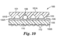
- Figure 10 illustrates a further alternative embodiment of an applique 100 according to the present invention.
- a cover layer or film 101 is provided having a top surface 101A and a bottom surface 101B.
- a backing layer or film 105 is provided having a top surface 105A and a bottom surface 105B.
- An adhesive 106 such as a hot melt adhesive or a pressure sensitive adhesive, is provided on top surface 105A of the backing layer 105.
- At least one optical fiber 108 is bonded between bottom surface 101B of the cover layer 101 and top surface 105A of backing layer 105 via adhesive 106.
- the bottom surface 101B of the cover layer 101 is provided with fiber alignment microstructure 103 which ensures proper positioning of the at least one optical fiber 108.
- such fiber alignment microstructure could be provided on top surface 105A of the backing layer.
- a second adhesive layer 110 is provided on bottom surface 105B of the backing layer.
- adhesive layer 110 is a pressure sensitive adhesive that allows repositionability.
- Crushable microstructure 112 similar to those described above, may also be provided on bottom surface 105B to enhance repositionability.
- Applique 100 is designed to mount on a substrate, such as a circuit board, with bottom surface 105B being adhered to the substrate with adhesive layer 110.
Abstract
A preformed fiber optic applique (10) having a backing layer (14) is
provided. The backing layer or film, has an adhesive coating (16) applied
thereon. At least one optical fiber (18) is routed and bonded to the adhesive
layer providing a continuous optical signal path from one end to another. A
releasable liner is releasably attached to the adhesive layer and positioned
to cover the backing layer including the at least one optical fiber.
Microstructures (42) are provided on the backing layer in one embodiment.
The microstructures are crushable structures that prevent the adhesive
from immediately adhering to a substrate.
Description
- The present invention relates to flexible optical circuits. In particular, the present invention relates to flexible optical circuits having a backing layer, an adhesive coating and a release liner for attachment to a substrate such as an electronic printed circuit board.
- The design of electronic circuits requires interconnections between devices for proper operation. With increased sophistication and operation speeds, design of functional interconnections requires careful engineering. The fastest data processing circuits and emerging technologies require large numbers of interconnects capable of carrying extremely high speed digital signals. Due to the increasing push for higher and higher speeds, engineers are facing fundamental limits in designing electronic interconnects.
- In an attempt to handle higher speeds, interconnection technology has turned to optical interconnects for next generation circuits. Optical circuits have bandwidth capabilities orders of magnitude beyond electrical circuits, and are inherently immune to electrical interference. In some known designs, discrete fiber optic cables and fiber bundles are used to interconnect devices. Known standard fiber optic connection technology employed to connect optical fibers to devices are adequate for small numbers of interconnections. However, as optical circuit density grows, the physical bulk of cables and connectors make this approach unwieldy, especially for compact designs.
- Attempts have been made to incorporate optical interconnects onto the surface of electronic circuit boards and substrates by constructing wave guides using optical polymers coated to the surface. An example of this is found in U. S. Patent No. 5,521,992 to Chun, et al. The technology of the '992 patent requires highly specialized tooling to generate each custom optical circuit thus standard circuit boards cannot be used. For simple circuits, tooling costs may be prohibitive. Waveguide fabrication is also difficult due to the small geometry of the guide regions, and optical quality of finished wave guides is poor due to limitations in optical polymer chemistry.
- Flexible optical interconnect circuit packs are also known in the art. An example of this is found in U.S. Patent No. 5,204,925 to Bonanni, et al. The known optical interconnect circuits have optical fibers bonded between two flexible substrates and have one or more optical connectors connected along the edges of the circuit pack. The connectors are then connected to one or more optical devices. These known devices are not adapted to bond to a substrate or circuit board.
- The concept of using high bond strength pressure sensitive adhesive coated laminating films is not new. However, there are certain problems associated with the known adhesive coated films. For instance, it is often difficult to obtain accurate positioning during film use. Improper placement, static charge, and accidental contact can all contribute to misalignment and immediate bonding to the surface in undesired positions. Because of the immediate aggressive bonding, if alignment is off, the film is often destroyed or seriously damaged attempting to remove the film for repositioning.
- One known solution to the above problem is to use a less aggressive adhesive so the user may remove or reposition the film in case of misalignment. This can result in poor long term adhesion. Another known solution is to use a partially cured adhesive material followed by a final curing process. This not only results in additional process step, but may be impractical for many applications. Yet another known solution is to prepare a surface wetted with a material that interferes with adhesion and then removing the wetting agent after final alignment is achieved. This approach can be messy and adds process steps.
- There is a continuing need for flexible optical circuits capable of being applied to new circuit board designs without changing board design and fabrication techniques. There is also a continued need for a laminating film that allows for repositioning of the optical circuits to achieve proper alignment.
- The present invention provides a flexible optical circuit applique that can be mounted on a circuit board without modifying the circuit board substrate or the electronic circuits. The optical circuit applique of the present invention is also repositionable. A method of manufacturing flexible optical circuit appliques is also provided.
- A preformed fiber optic applique is provided having a backing layer. The backing layer or film, has an adhesive coating applied thereon. At least one optical fiber is routed and bonded to the adhesive layer providing a continuous optical signal path from one end to another. A releasable liner is releasably attached to the adhesive layer and positioned to cover the backing layer including the at least one optical fiber.
- In one embodiment of the present invention, microstructures are provided on the backing layer. The microstructures are crushable structures that prevent the adhesive coating from immediately adhering to a substrate. This allows the film to be repositioned until proper alignment has been achieved. Upon the application of appropriate force, the microstructures will crush allowing the adhesive coating to bond the film to the substrate.
- A method of fabricating the fiber optic appliques of the present invention is also disclosed. The method includes the steps of providing a supply of backing layer and applying an adhesive coating to the backing layer. At least one fiber is then provided and placed on the adhesive coating. Pressure is then applied to the at least one fiber to secure it to the backing layer.
-
- Figure 1 is an exploded perspective view of an electrical circuit board and a flexible optical circuit applique according to the present invention.
- Figure 2a illustrates a preferred method of fabricating an optical circuit applique according to the present invention.
- Figure 2b illustrates an alternative method of fabricating an optical circuit applique according to the present invention.
- Figures 3a, b, c, and d illustrate alternative embodiments of a continuous web with fibers available for connectorization.
- Figures 4a, b, and c illustrate standard sections of optical circuit appliques according to the present invention.
- Figures 5a and b are top and side plan views of the flexible optical circuit having microreplicated structures according to the present invention.
- Figures 6a and b are top and side plan views of the flexible optical circuits of Figures 5a and b having optical fibers placed thereon.
- Figures 7a, b, c and d illustrate steps in a method for fabricating a flexible optical circuit and terminating the optical connectors at sockets according to the present invention.
- Figure 8 is a cross sectional view of a first alternative embodiment of the present invention.
- Figure 9 is a cross sectional view of a second alternative embodiment of the present invention.
- Figure 10 is a cross sectional view of a third alternative embodiment of the present invention.
-
- The present invention provides a flexible optical circuit applique having a flexible backing with fibers bonded thereto covered by a releasable liner. The optical appliques are intended to provide an easy means for adding optical circuits to electronic circuit boards or other substrates by laminating. The flexible optical circuits of the present invention can also be incorporated into new board designs without changing standard board design and fabrication techniques. The optical appliques of the present invention are also repositionable on a substrate prior to bonding.
- Figure 1 is a perspective view of a preferred embodiment of a flexible
optical circuit applique 10 according to the present invention. Also illustrated is a printedcircuit board 12 to whichapplique 10 is to be mounted.Applique 10 comprises adurable backing material 14 that is coated with a temporarilyrepositionable adhesive 16.Applique 10 also includesoptical fibers 18 bonded to backing 14 viaadhesive 16. The particular backing material used depends upon the particular application. For instance, if high durability is desired, a polyester-type backing would be used. If the applique is to be mounted on a curved substrate, a flexible backing material would be chosen. Examples of backing materials include vinyl, polyurethane, polyamide, and polyester. -
Adhesive 16 of the present invention is any temporarily repositionable adhesive. By temporarily repositionable, it is meant that the bond between the adhesive and the substrate is such that the material having the adhesive may be removed from the substrate without damaging either for a period of time or until the occurrence of a specified event which then permanently adheres the backing to the substrate. In the preferred embodiment, adhesive 16 is preferably a pressure sensitive adhesive. Pressure sensitive adhesives are known in the industry as a standard class of materials. They are adhesives, which in dry form (substantially solvent free except for residual solvent) are aggressively and permanently tacky at room temperature (approximately 15° to 25° C) and firmly adhere to a variety of similar surfaces upon mere contact without the need for more than manual pressure. The adhesives require no activation by water, solvent, or heat in order to exert a strong adhesive holding force towards such materials as paper, cellophane, glass, plastic, wood, and metals. The adhesives have a sufficiently cohesive holding and elastic nature such that, despite their aggressive tackiness, it can be handled with fingers and removed from smooth surfaces without leaving a substantial residue. For a more detailed discussion of pressure sensitive adhesives, reference should be made to U.S. Patent Nos. 5,296,277, 5,362,516 and 5,449,540, which are assigned to the Assignee of the present invention. - If adhesive 16 has low tack, e.g. is only slightly sticky to the touch and has low adhesion to certain types of surfaces, a release liner may not be required to cover the adhesive layer, and the
backing material 14 may act as a release liner when the film is rolled. - A light cured adhesive could be used with a transparent backing layer without departing from the spirit or scope of the invention. Such an adhesive would allow the film to be repositioned on a substrate until a light source, typically an ultra violet light, is applied through the transparent film which would then activate the adhesive to secure the film to the substrate. Nonpressure sensitive adhesives, thermally activated adhesives such as hot melt glue or solvent activated adhesives could also be used if desired, without departing from the spirit or scope of the invention. They are, however, less preferred embodiments because of the additional application steps and greater tendency to entrap air during application.
-
Optical fibers 18 of the present invention are preferably 80 to 100 micron glass (silica) diameter fibers with a special fiber coating described in U.S. Patent No. 5,381,504. Standard glass optical fibers have 125 micron outside diameters. By using glass fibers with diameters of 80 to 100 microns, the present invention can obtain bend radiuses as small as 0.25 inches (0.64 cm) while staying below a bending stress of 100 K psi. At a bend radius of 0.25 inches (0.64 cm), a fiber having a diameter of 125 microns has a bending stress of approximately 110 K psi and a fiber having a diameter of 200 microns has a bending stress of approximately 175 K psi. In the preferred embodiment of the present invention, bend radii of less than 0.3 inches (0.76 cm) are achieved at bend stresses of less than 100 K psi. - Figure 2a illustrates a preferred method of fabricating an applique according to the present invention. A
supply roll 20 of applique backing layer or film, 14 is provided, as is atakeup roll 22.Film 14 is precoated with anadhesive layer 16 and covered with areleasable liner 17. Asecond takeup roller 19 is provided to take awayreleasable liner 17 as illustrated. Arotating drum 24 is provided to movebacking film 14 fromsupply roll 20 totakeup roll 22.Multiple spools 28 offibers 18 are provided and are suspended abovebacking film 14. A laminatingroll spacing guide 30 is provided tospace fibers 18 as desired and to press the fibers ontobacking film 14 with sufficient force to activate pressure sensitive adhesive 16 tobond fibers 18 in place. Asecond supply roller 32 is provided carrying a secondreleasable liner 34 which releasably adheres to pressuresensitive adhesive 16. It should be noted thatfilm 14 may be a continuous and solid film or it may have holes formed therethrough for connectorization with optical circuit components, as will be described in greater detail below. - Figure 2b illustrates an alternative method of fabricating an applique according to the present invention. Figure 2b is similar to Figure 2a and thus like elements are correspondingly identified.
Supply roll 20 ofapplique backing film 14 is provided as is takeuproll 22. Rotatingdrum 24 is provided to movebacking film 14 fromsupply roll 20 totakeup roll 22. A pressure sensitiveadhesive coating device 26 is provided to apply a coating of pressure sensitive adhesive 16 tobacking film 14 as the backing film comes off ofsupply roll 20.Multiple spools 28 offibers 18 are provided and are suspended abovebacking film 14. Laminatingroll spacing guide 30 is provided tospace fibers 18 as desired and to press the fibers ontobacking film 14 with sufficient force to activate pressure sensitive adhesive 16 tobond fibers 18 in place.Second supply roller 32 is provided carryingrelease liner 34 which releasably adheres to pressuresensitive adhesive 16. - Fabricating appliques in a continuous web process, as illustrated in Figures 2a and 2b is a very cost effective way to fabricate the appliques. Depending upon the length of appliques desired, large numbers of standard appliques can easily be made from a single roll of
backing film 14. - Figures 3a - 3d illustrate alternative ways to make
fibers 18 available for connectorization in a continuous web process similar to those described in Figures 2a and 2b above. It should be noted that the examples given below are given only as exemplary ways to avail the fibers for connectorization, and the examples given are not meant to be an exhaustive list. The illustrations in Figures 3a-3d use some of the same components as used in Figures 1 and 2, therefore, like elements will be correspondingly identified. In Figure 3a,film 14 is coated withadhesive layer 16.Fibers 18 are bonded toadhesive layer 16 as previously described. Arelease strip 35 is provided across the width offilm 14 at predetermined intervals. The web is then cut at release strips 35. When applied to a substrate, release strips 35 prevent the ends of the individual applique section from adhering to the substrate thus allowing the ends of the fibers to be prepared for connectorization. It should be noted thatrelease strip 35 not need to extend across the entire width offilm 14. In Figure 3b, a series of receivingcavities 37 are formed throughfilm 14. The receiving cavities allow access tofibers 18 when the applique is adhered to a substrate. - Figure 3c illustrates a series of
mechanical alignment devices 39 spaced at desired locations along the continuous web.Alignment devices 39 provide mechanical alignment forfibers 18 and also function as release liners.Mechanical alignment devices 39 are preferably V grooved structures, but may also be U shaped or other shapes that provide adequate alignment forfibers 18. Afterfibers 18 have been adhered toadhesive surface 16 offilm 14,alignment device 39 may be removed prior to adhering to a substrate.Alignment device 39 could also be left in place with the applique adhered to a substrate. A connector assembly is then mounted around the fibers. In Figure 3d, anadhesiveless area 41 is provided onfilm 14. Thus, whenfilm 14 is adhered to substrate,fibers 18 are not adhered to the substrate inadhesiveless area 41. - The design of the applique according to the present invention including the number of fibers, the spacing of the fibers as well as the routing patterns can be done during the manufacturing process using a simple process control computer software program. Therefore, a board designer may layout a board and provide the manufacturer of the appliques of the present invention a layout of the board and an applique may be quickly and easily laid out by the process control program. Design and manufacture of appliques of the present invention may be conducted by, for example, Icon Industries, Euless, TX.
- Figures 4a, b and c illustrate some standard applique constructions. Figure 4a illustrates a 180°
bend applique 36. Figure 4b illustrates a 90°bend applique 38 and Figure 4c illustrates astraight applique 40. Additional standard applique constructions besides the ones illustrated in Figures 4a-c, such as 30° bends, 60° bends, 45° bends etc., are also considered within the spirit and scope of the present invention. Additionally a continuous web construction having alternating patterns may be formed. Standard appliques such as those discussed above can be premade and purchased ready to use. Because the appliques of Figures 4a-c may be purchased as ready to use appliques, the ends offibers 18 are also prepared for connectorization. - It should be noted that the fibers illustrated in Figures 4a-4c are shown stopping at the edge of the backing material. However, the fibers must be available for connectorization. Thus, any of the methods for making fibers available for connectorization, such as those described with respect to Figures 3a-3d, may be utilized.
-
Appliques 10 can be applied tocircuit boards 12 or other substrates by users during the manufacturing process, by removing release liners 34 (not shown in Figures 4a, 4b or 4c) from the adhesive surface and laminating the applique to the circuit board surface. It should be noted that multiple appliques can be placed over one another without degrading performance. - Figures 5a and b illustrate top and side plan views of flexible
optical circuit applique 10 incorporatingmicroreplicated structures 42 formed onbacking film 14 or inadhesive surface 16.Microreplicated structures 42 are provided to allow accurate positioning ofapplique 10. Improper placement or accidental contact of an active adhesive surface can contribute to misalignment and immediate bonding to the desired surface. Because the microstructures protrude up from backingfilm 14 and are taller than the depth ofadhesive coating 16,microstructures 42 prevent intimate contact betweenadhesive surface 16 andcircuit board 12 or other mounting surface.Structures 42 are crushable such that intimate contact betweenadhesive surface 16 andcircuit board 12 is obtained when suitable pressure is applied. Thus, the present invention may be repositioned until accurate alignment is achieved and further provides a high final bond strength after lamination. The microreplicated structures of the present invention are preferably approximately 15 micrometers high. Additionally, the density or durometer ofstructures 42 can be varied to provide lesser or greater resistance to crushing or forming. For a more detailed description ofmicrostructures 42, reference should be made to the above mentioned U.S. Patent Nos. 5,296,277, 5,362,516 and 5,449,540. It should be noted that alternative embodiments ofmicrostructures 42 or other repositionable adhesive constructions are also considered within the spirit and scope of the present invention. For instance, the adhesive may contain microspheres which may house a catalyst, either with or without the presence ofmicrostructures 42, such that when sufficient force is applied, the microspheres, and microstructures if present, are crushed and the catalyst is released, reacting with adhesive 16 to form an aggressive adhesive. - Figures 6a and b illustrate an
applique having microstructures 42 arranged in desired patterns such thatmicroreplicated structures 42 provide a guide forrouting fibers 18 in precise locations when bonded toadhesive surface 16. As illustrated in Figures 6a and 6b,fibers 18 fit intochannels 44 betweenstructures 42 and may thus be bonded toadhesive surface 16 without crushingstructures 42. As previously stated, the microstructures may be positioned as described to form any such pattern. -
Microstructures 42 may be formed onbacking film 14 before applyingadhesive coating 16. Or, they may be added toadhesive surface 16 after applique 10 is constructed andfibers 18 are bonded to film 14 by havingmicrostructures 42 picked up from an embossedrelease liner 34 which is attached immediately after fabrication. - Figures 7a-d illustrate steps for fabricating an applique according to the present invention that terminates
fibers 18 in sockets or connectors. To facilitate the fabrication process, a multichipmodule positioning fixture 52 is provided to give support to backingfilm 14 and to provide a pattern for cutting out receiving cavities where sockets are inserted. - One preferred method of fabricating an applique according to the present invention having sockets inserted therein is described below. It should be noted that the below described method is given as one example and should not be considered the only way to fabricate an applique according to the present invention. Backing
film 14 is unspooled and placed overpositioning fixture 52 as illustrated in Figure 7a. Pressuresensitive adhesive 16 is either applied tobacking film 14 orbacking film 14 already has an adhesive layer coating thereon.Optical fibers 18 are then routed to desired positions onbacking film 14. The paths taken byfibers 18 may follow parallel or individual routes, and provide a continuous signal path from one end to another. The optical circuit paths may also cross previously installed fibers producing multiple layers to optimize path geometry. Oncefibers 18 are routed appropriately, they are bonded tobacking film 14 by applying sufficient force to activate pressuresensitive adhesive 16. At this point, backingfilm 14 is cut atpositions 49 where sockets are to be installed. As shown in Fig. 7b, the ends offibers 18 are then cut, cleaved, sawed, polished or otherwise prepared for termination depending on user requirements. For ease of connectorization,optical fibers 18 are usually terminated in connectors orsockets 50. After preparing fiber ends,socket 50 is inserted through the hole formed in backing film 14 (Fig. 7c). Finally, as shown in Fig. 7d, a circuit board orother substrate 12 is bonded tobacking film 14 and the backing film is cut to fit in the circuit board. - The appliques of the present invention allow the optical paths formed by
fibers 18 to be pretested before applying tocircuit board 12 or any other substrate. Another benefit of the present invention is thatfibers 18 are protected byfilm 14 when applied tocircuit board 12. As previously stated, the backing film may vary depending upon the application. If greater protection forfibers 18 is needed, a stronger or thicker backing may be chosen. A further benefit of the appliques of the present invention is that the risk of damaging a valuable circuit board is greatly reduced. Typically, there is already substantial value invested in a circuit board at the time of providing electrical or optical connections. Using the present invention, the circuit boards do not need to be destroyed if proper alignment is not achieved or if the applique is not working. If waveguides are used and a mistake is made, the circuit board is usually ruined. - Figure 8 illustrates an alternative embodiment of an
applique 68 according to the present invention. As stated above, backingfilm 14 protectsfibers 18 when applied tocircuit board 12. However, it may be desirable to have a protecting film betweenfibers 18 andboard 12. Thus, as illustrated in Figure 8, afirst backing film 60 is provided having atop surface 62 and abottom surface 64. A firstadhesive layer 66 is provided onbottom surface 64. Asecond backing film 69 is provided having atop surface 70 and abottom surface 72. Asecond adhesive layer 74 is provided onbottom surface 74. At least oneoptical fiber 76 is sandwiched betweenbacking films Applique 68 is then mounted to a substrate such as a circuit board and bonded in place withadhesive 74. As with the embodiment described above, microstructures (not shown in Figure 8) could also be included to allow for repositionability or fiber alignment. - Figure 9 illustrates a further alternative embodiment of an
applique 79 according to the present invention. A backing layer orfilm 80 is provided having atop surface 82 and abottom surface 84. An adhesive 86, such as a hot melt adhesive, is provided ontop surface 82. At least one optical fiber (not shown) may be bonded totop surface 82 viaadhesive 86. Asecond adhesive layer 90 is provided onbottom surface 84. Preferablyadhesive layer 90 is a pressure sensitive adhesive that allows repositionability.Microstructure 92, similar to those described above, may also be provided onbottom surface 84.Applique 79 is designed to mount on a substrate, such as a circuit board, withbottom surface 84 being adhered to the substrate withadhesive layer 90. - Figure 10 illustrates a further alternative embodiment of an
applique 100 according to the present invention. A cover layer orfilm 101 is provided having atop surface 101A and abottom surface 101B. A backing layer orfilm 105 is provided having atop surface 105A and abottom surface 105B. An adhesive 106 such as a hot melt adhesive or a pressure sensitive adhesive, is provided ontop surface 105A of thebacking layer 105. At least oneoptical fiber 108 is bonded betweenbottom surface 101B of thecover layer 101 andtop surface 105A ofbacking layer 105 viaadhesive 106. Thebottom surface 101B of thecover layer 101 is provided withfiber alignment microstructure 103 which ensures proper positioning of the at least oneoptical fiber 108. Alternatively, such fiber alignment microstructure could be provided ontop surface 105A of the backing layer. A secondadhesive layer 110 is provided onbottom surface 105B of the backing layer. Preferably,adhesive layer 110 is a pressure sensitive adhesive that allows repositionability.Crushable microstructure 112, similar to those described above, may also be provided onbottom surface 105B to enhance repositionability.Applique 100 is designed to mount on a substrate, such as a circuit board, withbottom surface 105B being adhered to the substrate withadhesive layer 110. - Although a certain preferred embodiment has been shown and described, it should be understood that many changes and modifications could be made therein without departing from the spirit or scope of the appending claims.
Claims (12)
- A device for applying a fiber optic arrangement to a substrate (12) comprising:characterized in thata backing layer (14),an adhesive layer (16) applied to the backing layer, andat least one optical fiber (18) bonded to the backing layer (14),the adhesive layer (16) is a temporarily repositionable adhesive layer providing a temporarily repositionable bond between the adhesive and the substrate (12) so that the backing layer (14) may be removed from the substrate (12) without damage andmicrostructures (42) are formed on the backing layer (14) for guiding the at least one optical fiber (18).
- The device as in claim 1 further comprising a releasable liner releasably attached to the temporarily repositionable adhesive layer (16) positioned over the at least one optical fiber (18).
- The device as in claim 1 or 2 wherein the temporarily repositionable adhesive (16) is selected from the group consisting of:pressure sensitive adhesives having crushable microstructures, andpartially cured adhesives containing crushable microspheres with curing catalyst inside.
- The device as in any of the claims 1 to 3 whereinthe backing layer (80) has first and second sides (84,82),the temporarily repositionable adhesive (90) is applied to the first side of the backing layer (80), wherein a second adhesive (86) is applied to the second side (82) of the backing layer (80), and wherein the at least one optical fiber (18) is bonded to the second adhesive (86).
- The device as in claim 4 wherein the second adhesive (86) is selected from the group consisting of:pressure sensitive adhesives having crushable microstructures, andpartially cured adhesives containing crushable microspheres with curing catalyst inside.
- The device as in any of the claims 1 to 5, wherein the microstructures (42) are positioned to form channels (44) and wherein the at least one optical fiber (18) is positioned in the channels (44).
- A device for applying a fiber optic arrangement to a substrate (12) comprising:a backing layer (14),a plurality of microstructures (42) formed on the backing layer (14) in a desired pattern to form a plurality of channels (44),an adhesive layer (16) applied to the backing layer (14) wherein the adhesive layer (16) has a desired depth and wherein the plurality of microstructures (42) protrude from the backing layer (14) above the desired depth of the adhesive layer (16), andat least one optical fiber (18) bonded to the backing layer (14) in at least one of the plurality of channels (44).
- The device as in any of the claims 1 to 7, wherein the microstructures (42) are crushable.
- The device as in claim 7 or 8 wherein the adhesive layer (16) is a temporarily repositionable adhesive providing a temporarily repositionable bond between the adhesive and the substrate (12) so that the backing layer (14) may be removed from the substrate (12) without damage.
- The device as in claim 9, wherein the temporarily repositionable adhesive (16) is selected from the group consisting of:pressure sensitive adhesives having crushable microstructures, andpartially cured adhesives containing crushable microspheres with curing catalyst inside.
- A method of forming a device for applying a fiber optic arrangement to a substrate (12), the device having a backing layer, an adhesive layer and at least one optical fiber bonded thereto, the method comprising the steps of:providing a supply of backing layer (14) including microstructures (42) formed on the backing layer (14) for guiding at least one optical fiber (18),applying an adhesive coating (16) to the backing layer (14),providing at least one optical fiber (18),placing the at least one optical fiber (18) on the adhesive coating (16) so as to be guided on the backing layer (14) in a desired pattern, andapplying pressure to the at least one optical fiber (18) to secure the optical fiber (18) to the backing layer (14) with the adhesive coating (16).
- The method of claim 11 whereinthe step of providing a backing layer (14) comprises providing a continuous length of backing layer film and extending the backing layer film between a supply roll (20) and a takeup roll (22) in a continuous web process,the step of providing at least one optical fiber (18) includes providing a plurality of spools (28) of optical fibers (18), andthe step of placing the at least one optical fiber (18) on the backing layer (14) in a desired pattern includes rolling the fibers (18) onto the backing layer (14) while the layer (14) moves from the supply roll (20) to the takeup roll (22)
Applications Claiming Priority (3)
| Application Number | Priority Date | Filing Date | Title |
|---|---|---|---|
| US08/775,849 US5902435A (en) | 1996-12-31 | 1996-12-31 | Flexible optical circuit appliques |
| US775849 | 1996-12-31 | ||
| EP97933129A EP0950203B1 (en) | 1996-12-31 | 1997-05-08 | Flexible optical circuit appliques |
Related Parent Applications (1)
| Application Number | Title | Priority Date | Filing Date |
|---|---|---|---|
| EP97933129A Division EP0950203B1 (en) | 1996-12-31 | 1997-05-08 | Flexible optical circuit appliques |
Publications (1)
| Publication Number | Publication Date |
|---|---|
| EP1202094A1 true EP1202094A1 (en) | 2002-05-02 |
Family
ID=25105706
Family Applications (2)
| Application Number | Title | Priority Date | Filing Date |
|---|---|---|---|
| EP01129469A Withdrawn EP1202094A1 (en) | 1996-12-31 | 1997-05-08 | Flexible optical circuit appliques |
| EP97933129A Expired - Lifetime EP0950203B1 (en) | 1996-12-31 | 1997-05-08 | Flexible optical circuit appliques |
Family Applications After (1)
| Application Number | Title | Priority Date | Filing Date |
|---|---|---|---|
| EP97933129A Expired - Lifetime EP0950203B1 (en) | 1996-12-31 | 1997-05-08 | Flexible optical circuit appliques |
Country Status (6)
| Country | Link |
|---|---|
| US (2) | US5902435A (en) |
| EP (2) | EP1202094A1 (en) |
| JP (1) | JP3924627B2 (en) |
| CA (1) | CA2274568A1 (en) |
| DE (1) | DE69723867T2 (en) |
| WO (1) | WO1998029771A1 (en) |
Cited By (1)
| Publication number | Priority date | Publication date | Assignee | Title |
|---|---|---|---|---|
| EP1837688A1 (en) * | 2006-06-20 | 2007-09-26 | Honeywell International, Inc. | Fiber pattern applicator system and method |
Families Citing this family (57)
| Publication number | Priority date | Publication date | Assignee | Title |
|---|---|---|---|---|
| CN1305412A (en) * | 1998-06-15 | 2001-07-25 | 美国3M公司 | Multi-component unidirectional graphic article |
| SE514117C2 (en) * | 1999-03-12 | 2001-01-08 | Ericsson Telefon Ab L M | Method and apparatus for forming a ribbon-like structure of loose optical fibers, as well as adhesive tape |
| US6927315B1 (en) * | 1999-07-30 | 2005-08-09 | 3M Innovative Properties Company | Adhesive composite having distinct phases |
| AUPR245701A0 (en) | 2001-01-10 | 2001-02-01 | Silverbrook Research Pty Ltd | An apparatus (WSM10) |
| US6599031B2 (en) | 2001-09-12 | 2003-07-29 | Intel Corporation | Optical/electrical interconnects and package for high speed signaling |
| US7275562B2 (en) * | 2001-10-17 | 2007-10-02 | Agilent Technologies, Inc. | Extensible spiral for flex circuit |
| US6587631B2 (en) * | 2001-12-04 | 2003-07-01 | Harris Corporation | Fiber-optic backplane method and apparatus |
| US6538207B1 (en) | 2002-01-18 | 2003-03-25 | Agilent Technologies, Inc. | Strain relief structures for lead connections |
| US7532782B2 (en) * | 2002-04-18 | 2009-05-12 | Pivotal Decisions Llc | Flexible optical circuit apparatus and method |
| US6947652B2 (en) * | 2002-06-14 | 2005-09-20 | 3M Innovative Properties Company | Dual-band bend tolerant optical waveguide |
| WO2004012617A2 (en) * | 2002-08-02 | 2004-02-12 | Sdgi Holdings, Inc. | Systems and techniques for illuminating a surgical space |
| US7223233B2 (en) * | 2002-08-02 | 2007-05-29 | Warsaw Orthopedic, Inc. | Systems and techniques for illuminating a surgical space |
| JP3866172B2 (en) * | 2002-08-27 | 2007-01-10 | 富士通株式会社 | Optical module and fiber sheet |
| US20040042705A1 (en) * | 2002-08-27 | 2004-03-04 | Uchida Toshi K. | Embedded optical coupling in circuit boards |
| US7149376B2 (en) * | 2002-08-27 | 2006-12-12 | Ibiden Co., Ltd. | Embedded optical coupling in circuit boards |
| US6801693B1 (en) * | 2002-10-16 | 2004-10-05 | International Business Machines Corporation | Optical backplane array connector |
| US6917746B2 (en) * | 2002-12-17 | 2005-07-12 | 3M Innovative Properties Company | Apparatus and method for creating a fiber optic circuit |
| USH2144H1 (en) * | 2003-01-14 | 2006-02-07 | Tyco Electronics Corporation | Layered optical circuit |
| US20040161212A1 (en) * | 2003-02-18 | 2004-08-19 | Sun Maurice X. | Fiber optic apparatus |
| US6873781B2 (en) | 2003-03-11 | 2005-03-29 | 3M Innovative Properties Company | Optical fiber wiring board |
| US6862407B2 (en) * | 2003-05-09 | 2005-03-01 | Charles H. Gale | Camera stabilizer platform and camcorder therefor |
| US20040223081A1 (en) | 2003-05-09 | 2004-11-11 | Gale Charles H. | Camera stabilizer platform and camcorder therefor |
| US7130498B2 (en) * | 2003-10-16 | 2006-10-31 | 3M Innovative Properties Company | Multi-layer optical circuit and method for making |
| EP1706041B1 (en) | 2003-12-18 | 2015-11-18 | DePuy Spine, Inc. | Surgical retractor systems, illuminated cannulas, and methods of use |
| US7130511B2 (en) * | 2004-03-30 | 2006-10-31 | Motorola, Inc. | Flexible active signal cable |
| US7130516B2 (en) * | 2004-08-31 | 2006-10-31 | 3M Innovative Properties Company | Triple-band bend tolerant optical waveguide |
| US7130515B2 (en) * | 2004-08-31 | 2006-10-31 | 3M Innovative Properties Company | Triple-band bend tolerant optical waveguide |
| US20060099371A1 (en) * | 2004-11-09 | 2006-05-11 | Gamer Graffix Worldwide, Llc | Decorative laminate |
| US7200295B2 (en) * | 2004-12-07 | 2007-04-03 | Reflex Photonics, Inc. | Optically enabled hybrid semiconductor package |
| US20060224045A1 (en) * | 2005-03-31 | 2006-10-05 | Depuy Spine, Inc. | Integrated access device and light source for surgical procedures |
| US20060285339A1 (en) * | 2005-06-20 | 2006-12-21 | William Frasier | Adjustable light source holder |
| US20070100210A1 (en) * | 2005-11-02 | 2007-05-03 | Depuy Spine, Inc. | Illuminated surgical access system including a surgical access device and coupled light emitter |
| US7981031B2 (en) | 2006-01-04 | 2011-07-19 | Depuy Spine, Inc. | Surgical access devices and methods of minimally invasive surgery |
| US7758501B2 (en) | 2006-01-04 | 2010-07-20 | Depuy Spine, Inc. | Surgical reactors and methods of minimally invasive surgery |
| US7918792B2 (en) | 2006-01-04 | 2011-04-05 | Depuy Spine, Inc. | Surgical retractor for use with minimally invasive spinal stabilization systems and methods of minimally invasive surgery |
| US7955257B2 (en) | 2006-01-05 | 2011-06-07 | Depuy Spine, Inc. | Non-rigid surgical retractor |
| US8409088B2 (en) | 2006-01-18 | 2013-04-02 | Invuity, Inc. | Retractor illumination system |
| US8430813B2 (en) | 2006-05-26 | 2013-04-30 | Depuy Spine, Inc. | Illuminated surgical access system including a surgical access device and integrated light emitter |
| US8047987B2 (en) * | 2006-05-26 | 2011-11-01 | Invuity, Inc. | Blade insert illuminator |
| JP4664236B2 (en) * | 2006-05-31 | 2011-04-06 | 株式会社巴川製紙所 | Optical fiber converging member and optical fiber assembly |
| KR100871252B1 (en) * | 2007-01-19 | 2008-11-28 | 삼성전자주식회사 | Photoelectronic wired flexible printed circuit board using optical fiber |
| US20080287937A1 (en) * | 2007-05-15 | 2008-11-20 | Warsaw Orthopedic, Inc. | Surgical Instrument for Illuminating and Monitoring a Surgical Site |
| US20090010021A1 (en) * | 2007-07-06 | 2009-01-08 | Smith Jeffrey T | Recreational apparatus and method of making the same |
| JP4870627B2 (en) * | 2007-08-06 | 2012-02-08 | 日東電工株式会社 | Optical waveguide film and manufacturing method thereof |
| US8088066B2 (en) | 2007-10-24 | 2012-01-03 | Invuity, Inc. | Blade insert illuminator |
| US11382711B2 (en) | 2008-08-13 | 2022-07-12 | Invuity, Inc. | Cyclo olefin polymer and copolymer medical devices |
| US8346043B2 (en) * | 2009-07-30 | 2013-01-01 | Jds Uniphase Corporation | Fiber tray |
| JP2012150360A (en) * | 2011-01-20 | 2012-08-09 | Mitsubishi Cable Ind Ltd | Optical fiber wiring structure and manufacturing method thereof |
| JP5522076B2 (en) * | 2011-02-16 | 2014-06-18 | 日立金属株式会社 | Flexible flat optical cable |
| US8687934B2 (en) * | 2011-03-21 | 2014-04-01 | Tyco Electronics Corporation | Fiber optic component holders and enclosures and methods including the same |
| EP2717044A1 (en) * | 2012-10-03 | 2014-04-09 | Metrohm Ag | Method for detecting analytes |
| CN108603990B (en) * | 2016-01-12 | 2021-05-28 | 康普连通比利时私人有限公司 | Cable management arrangement device |
| WO2018006173A1 (en) | 2016-07-07 | 2018-01-11 | Atomic Energy Of Canada Limited / Énergie Atomique Du Canada Limitée | Apparatus and method for adhering a filament to a surface |
| EP3555684A4 (en) * | 2016-12-13 | 2020-07-22 | Corning Research And Development Corporation | Drop cable with attachment webbing |
| US10459160B2 (en) | 2017-01-31 | 2019-10-29 | Corning Optical Communications LLC | Glass waveguide assemblies for OE-PCBs and methods of forming OE-PCBs |
| US11397295B2 (en) * | 2018-04-06 | 2022-07-26 | Commscope Technologies Llc | Flexible organizer and self-supporting unit |
| JP7135871B2 (en) | 2019-01-10 | 2022-09-13 | 日本電信電話株式会社 | optical module |
Citations (5)
| Publication number | Priority date | Publication date | Assignee | Title |
|---|---|---|---|---|
| US3314838A (en) * | 1964-08-26 | 1967-04-18 | Minnesota Mining & Mfg | Pressure sensitive adhesives containing hollow spheroidal particles |
| US3860405A (en) * | 1972-11-13 | 1975-01-14 | Western Electric Co | Bonding of optical components |
| US3943021A (en) * | 1972-02-07 | 1976-03-09 | Lindsey Richard W | Optical data processing system |
| EP0587336A2 (en) * | 1992-08-28 | 1994-03-16 | AT&T Corp. | Optical fiber interconnection apparatus and methods |
| US5362516A (en) * | 1992-06-26 | 1994-11-08 | Minnesota Mining And Manufacturing Company | Method of preparing an adhesive article |
Family Cites Families (28)
| Publication number | Priority date | Publication date | Assignee | Title |
|---|---|---|---|---|
| US3777154A (en) * | 1972-02-07 | 1973-12-04 | R Lindsey | Optical data processing system |
| US4005312A (en) * | 1973-11-08 | 1977-01-25 | Lemelson Jerome H | Electro-optical circuits and manufacturing techniques |
| US4138193A (en) * | 1977-09-27 | 1979-02-06 | General Cable Corporation | Multiple fiber laminate for optical waveguides |
| US4307386A (en) * | 1977-12-09 | 1981-12-22 | Roderick Iain Davidson | Security system and strip or strand incorporating fibre-optic wave guide means therefor |
| US4529645A (en) * | 1982-10-19 | 1985-07-16 | Minnesota Mining And Manufacturing Company | Polyethylene-terephthalate-backed adhesive tape or extreme dimensional stability |
| FR2574562B1 (en) * | 1984-12-10 | 1988-02-05 | Commissariat Energie Atomique | OPTICAL INFORMATION CONDUCTOR AND METHOD OF ORDERLY PLACING OPTICAL FIBERS FOR THE MANUFACTURE OF THIS CONDUCTOR |
| US4597030A (en) * | 1985-01-31 | 1986-06-24 | American Hospital Supply Corporation | Surgical illuminator |
| US4650704A (en) * | 1985-03-06 | 1987-03-17 | Stik-Trim Industries, Inc. | Self-adhesive wall covering or the like and method of making same |
| IL80276A0 (en) * | 1986-10-10 | 1987-01-30 | Ispra Israel Prod Res Co Ltd | Wallpaper comprising an optical fibre |
| US4783354A (en) * | 1986-12-15 | 1988-11-08 | Coated Sales, Inc. | Adherable, yet removable sheet material |
| DE3910710A1 (en) * | 1989-04-03 | 1990-10-04 | Standard Elektrik Lorenz Ag | OPTICAL-ELECTRICAL MULTIPLE CONNECTION |
| US5076881A (en) * | 1989-07-14 | 1991-12-31 | At&T Bell Laboratories | Apparatus for fabricating an optical fiber ribbon |
| US5046800A (en) * | 1990-10-09 | 1991-09-10 | At&T Bell Laboratories | Article comprising a passive optical waveguide |
| US5134470A (en) * | 1991-06-10 | 1992-07-28 | Hughes Aircraft Company | Optical fiber interconnections and method of forming same |
| US5226105A (en) * | 1991-06-27 | 1993-07-06 | Poly-Optical Products, Inc. | Fiber optic backlighting panel and dot process for making same |
| US5160569A (en) * | 1991-08-08 | 1992-11-03 | Siecor Corporation | Tool for preparing optical ribbons |
| US5204925A (en) * | 1991-09-11 | 1993-04-20 | At&T Bell Laboratories | Optical interconnection of circuit packs |
| WO1993005123A1 (en) * | 1991-09-12 | 1993-03-18 | Minnesota Mining And Manufacturing Company | Patterned pressure sensitive adhesive transfer tape |
| US5327513A (en) * | 1992-05-28 | 1994-07-05 | Raychem Corporation | Flat cable |
| US5292390A (en) * | 1992-09-30 | 1994-03-08 | At&T Bell Laboratories | Optical fiber encapsulating techniques |
| US5381504A (en) * | 1993-11-15 | 1995-01-10 | Minnesota Mining And Manufacturing Company | Optical fiber element having a permanent protective coating with a Shore D hardness value of 65 or more |
| US5394504A (en) * | 1994-02-24 | 1995-02-28 | At&T Corp. | Optical fiber encapsulation techniques |
| US5521992A (en) * | 1994-08-01 | 1996-05-28 | Motorola, Inc. | Molded optical interconnect |
| JPH08151755A (en) * | 1994-11-30 | 1996-06-11 | Osada Giken Kk | Sheet for sticking on surface of building and building-surface treating method |
| US5611017A (en) * | 1995-06-01 | 1997-03-11 | Minnesota Mining And Manufacturing Co. | Fiber optic ribbon cable with pre-installed locations for subsequent connectorization |
| US5676787A (en) * | 1995-06-07 | 1997-10-14 | Borden Decorative Products, Inc. | Method for making repositionable wall covering and intermediate for same |
| US5835646A (en) * | 1995-09-19 | 1998-11-10 | Fujitsu Limited | Active optical circuit sheet or active optical circuit board, active optical connector and optical MCM, process for fabricating optical waveguide, and devices obtained thereby |
| US6005991A (en) * | 1997-11-26 | 1999-12-21 | Us Conec Ltd | Printed circuit board assembly having a flexible optical circuit and associated fabrication method |
-
1996
- 1996-12-31 US US08/775,849 patent/US5902435A/en not_active Expired - Lifetime
-
1997
- 1997-05-08 EP EP01129469A patent/EP1202094A1/en not_active Withdrawn
- 1997-05-08 DE DE69723867T patent/DE69723867T2/en not_active Expired - Fee Related
- 1997-05-08 CA CA002274568A patent/CA2274568A1/en not_active Abandoned
- 1997-05-08 EP EP97933129A patent/EP0950203B1/en not_active Expired - Lifetime
- 1997-05-08 WO PCT/US1997/008064 patent/WO1998029771A1/en active IP Right Grant
- 1997-05-08 JP JP52996598A patent/JP3924627B2/en not_active Expired - Lifetime
-
1998
- 1998-12-08 US US09/207,559 patent/US6427034B1/en not_active Expired - Lifetime
Patent Citations (5)
| Publication number | Priority date | Publication date | Assignee | Title |
|---|---|---|---|---|
| US3314838A (en) * | 1964-08-26 | 1967-04-18 | Minnesota Mining & Mfg | Pressure sensitive adhesives containing hollow spheroidal particles |
| US3943021A (en) * | 1972-02-07 | 1976-03-09 | Lindsey Richard W | Optical data processing system |
| US3860405A (en) * | 1972-11-13 | 1975-01-14 | Western Electric Co | Bonding of optical components |
| US5362516A (en) * | 1992-06-26 | 1994-11-08 | Minnesota Mining And Manufacturing Company | Method of preparing an adhesive article |
| EP0587336A2 (en) * | 1992-08-28 | 1994-03-16 | AT&T Corp. | Optical fiber interconnection apparatus and methods |
Non-Patent Citations (1)
| Title |
|---|
| SHAHID M A ET AL: "Flexible optical backplane interconnections", PROCEEDINGS OF THE THIRD INTERNATIONAL CONFERENCE ON MASSIVELY PARALLEL PROCESSING USING OPTICAL INTERCONNECTIONS (CAT. NO.96TB100092), PROCEEDINGS OF MASSIVELY PARALLEL PROCESSING USING OPTICAL INTERCONNECTIONS, MAUI, HI, USA, 27-29 OCT. 1996, ISBN 0-8186-7591-8, 1996, LOS ALAMITOS, CA, USA, IEEE COMPUT. SOC. PRESS, USA, pages 178 - 185, XP002044019 * |
Cited By (1)
| Publication number | Priority date | Publication date | Assignee | Title |
|---|---|---|---|---|
| EP1837688A1 (en) * | 2006-06-20 | 2007-09-26 | Honeywell International, Inc. | Fiber pattern applicator system and method |
Also Published As
| Publication number | Publication date |
|---|---|
| EP0950203A1 (en) | 1999-10-20 |
| DE69723867T2 (en) | 2004-07-29 |
| WO1998029771A1 (en) | 1998-07-09 |
| US6427034B1 (en) | 2002-07-30 |
| JP3924627B2 (en) | 2007-06-06 |
| CA2274568A1 (en) | 1998-07-09 |
| US5902435A (en) | 1999-05-11 |
| DE69723867D1 (en) | 2003-09-04 |
| JP2001507813A (en) | 2001-06-12 |
| EP0950203B1 (en) | 2003-07-30 |
Similar Documents
| Publication | Publication Date | Title |
|---|---|---|
| US5902435A (en) | Flexible optical circuit appliques | |
| EP1103832B1 (en) | Optical interconnection apparatus and method of fabricating same | |
| KR100415958B1 (en) | A process for production of an optical interconnection apparatus | |
| CA2323481C (en) | Optical connection component and method of producing the same | |
| EP1361464B1 (en) | Optical interconnection apparatus | |
| EP1182471B1 (en) | Device for optical connection | |
| JP2008216917A (en) | Fixture for attaching adhesive connecting member | |
| JP4051822B2 (en) | Optical circuit board and manufacturing method thereof | |
| JP2000517437A (en) | Connector body | |
| JP3326402B2 (en) | Optical connection parts | |
| JP3704517B2 (en) | Optical connecting component and method for manufacturing the same | |
| JP3545261B2 (en) | Optical connection parts | |
| JP2001296436A (en) | Method for manufacturing optical circuit board | |
| JP2001249233A (en) | Optically connecting parts and their manufacturing method | |
| JP2000121879A (en) | Optical connection member and its manufacture |
Legal Events
| Date | Code | Title | Description |
|---|---|---|---|
| PUAI | Public reference made under article 153(3) epc to a published international application that has entered the european phase |
Free format text: ORIGINAL CODE: 0009012 |
|
| AC | Divisional application: reference to earlier application |
Ref document number: 950203 Country of ref document: EP |
|
| AK | Designated contracting states |
Kind code of ref document: A1 Designated state(s): DE FR GB SE |
|
| 17P | Request for examination filed |
Effective date: 20021009 |
|
| 17Q | First examination report despatched |
Effective date: 20021128 |
|
| AKX | Designation fees paid |
Free format text: DE FR GB SE |
|
| STAA | Information on the status of an ep patent application or granted ep patent |
Free format text: STATUS: THE APPLICATION IS DEEMED TO BE WITHDRAWN |
|
| 18D | Application deemed to be withdrawn |
Effective date: 20030611 |