EP1204152A2 - External electrodes for piezoceramic stack actuators - Google Patents
External electrodes for piezoceramic stack actuators Download PDFInfo
- Publication number
- EP1204152A2 EP1204152A2 EP01126097A EP01126097A EP1204152A2 EP 1204152 A2 EP1204152 A2 EP 1204152A2 EP 01126097 A EP01126097 A EP 01126097A EP 01126097 A EP01126097 A EP 01126097A EP 1204152 A2 EP1204152 A2 EP 1204152A2
- Authority
- EP
- European Patent Office
- Prior art keywords
- base metallization
- external electrodes
- actuator
- layer
- lines
- Prior art date
- Legal status (The legal status is an assumption and is not a legal conclusion. Google has not performed a legal analysis and makes no representation as to the accuracy of the status listed.)
- Granted
Links
Images
Classifications
-
- H—ELECTRICITY
- H10—SEMICONDUCTOR DEVICES; ELECTRIC SOLID-STATE DEVICES NOT OTHERWISE PROVIDED FOR
- H10N—ELECTRIC SOLID-STATE DEVICES NOT OTHERWISE PROVIDED FOR
- H10N30/00—Piezoelectric or electrostrictive devices
- H10N30/80—Constructional details
- H10N30/87—Electrodes or interconnections, e.g. leads or terminals
- H10N30/872—Connection electrodes of multilayer piezoelectric or electrostrictive devices, e.g. external electrodes
-
- H—ELECTRICITY
- H10—SEMICONDUCTOR DEVICES; ELECTRIC SOLID-STATE DEVICES NOT OTHERWISE PROVIDED FOR
- H10N—ELECTRIC SOLID-STATE DEVICES NOT OTHERWISE PROVIDED FOR
- H10N30/00—Piezoelectric or electrostrictive devices
- H10N30/01—Manufacture or treatment
- H10N30/06—Forming electrodes or interconnections, e.g. leads or terminals
- H10N30/063—Forming interconnections, e.g. connection electrodes of multilayered piezoelectric or electrostrictive parts
-
- H—ELECTRICITY
- H10—SEMICONDUCTOR DEVICES; ELECTRIC SOLID-STATE DEVICES NOT OTHERWISE PROVIDED FOR
- H10N—ELECTRIC SOLID-STATE DEVICES NOT OTHERWISE PROVIDED FOR
- H10N30/00—Piezoelectric or electrostrictive devices
- H10N30/50—Piezoelectric or electrostrictive devices having a stacked or multilayer structure
- H10N30/508—Piezoelectric or electrostrictive devices having a stacked or multilayer structure adapted for alleviating internal stress, e.g. cracking control layers
Landscapes
- Engineering & Computer Science (AREA)
- Manufacturing & Machinery (AREA)
- General Electrical Machinery Utilizing Piezoelectricity, Electrostriction Or Magnetostriction (AREA)
- Fuel-Injection Apparatus (AREA)
Abstract
Description
Die Erfindung betrifft die Außenelektroden an piezokeramischen Vielschichtaktoren sowie ein Verfahren zu ihrer Herstellung.The invention relates to the external electrodes on piezoceramic Multi-layer actuators and a process for their manufacture.
Der Aufbau und die Herstellung von Aktoren und ihren Außenelektroden wird unter anderem ausführlich beschrieben in DE 33 30538 A1, DE 40 36 287 C2, US 5 281 885, US 4 845 399, US 5 406 164 und JP 07-226541 A.The construction and manufacture of actuators and their outer electrodes is used among others described in detail in DE 33 30538 A1, DE 40 36 287 C2, US 5,281,885, US 4,845,399, US 5,406,164 and JP 07-226541 A.
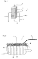
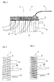
Ein piezokeramischer Vielschichtaktor ist schematisch in Figur 1 dargestellt. Die
Figur 2 zeigt in einem vergrößerten Ausschnitt den Aufbau der Außenelektrode
nach dem Stand der Technik und die Figur 3 einen typischen Rissverlauf nach
106 Belastungszyklen in dem keramischen Werkstoff unter einer Außenelektrode
nach dem Stand der Technik. Piezokeramische Vielschichtaktoren 1 werden als
Monolithen ausgeführt, das heißt, sie bestehen aus gestapelten dünnen
Schichten 2 piezoelektrisch aktiven Materials, beispielsweise Blei-Zirkonat-Titanat
(PZT), mit dazwischen angeordneten leitfähigen Innenelektroden 7, die
alternierend an die Aktoroberfläche geführt werden. Das aktive Material wird als
sogenannte Grün-Folie vor dem Sintern durch ein Siebdruckverfahren mit
Innenelektroden 7 versehen, zu einem Stapel verpresst, pyrolysiert und dann
gesintert, wodurch ein monolithischer Vielschichtaktor 1 entsteht.A piezoceramic multilayer actuator is shown schematically in FIG. 1. FIG. 2 shows an enlarged section of the structure of the outer electrode according to the prior art, and FIG. 3 shows a typical crack course after 10 6 load cycles in the ceramic material under an outer electrode according to the prior art. Piezoceramic multilayer actuators 1 are designed as monoliths, that is to say they consist of stacked
Außenelektroden 3, 4, 8 verbinden die Innenelektroden 7. Dadurch werden die
Innenelektroden 7 jeweils auf einer Seite des Aktors 1 elektrisch parallel
geschaltet und so zu einer Gruppe zusammengefasst. Die Außenelektroden 3, 4
sind die Anschlusspole des Aktors. Wird eine elektrische Spannung an die
Anschlusspole gelegt, so wird diese auf alle Innenelektroden 7 parallel
übertragen und verursacht ein elektrisches Feld in allen Schichten des aktiven
Materials, das sich dadurch mechanisch verformt. Die Summe aller dieser
mechanischen Verformungen steht an den Endflächen des Aktors als nutzbare
Dehnung 6 und/oder Kraft zur Verfügung.
Die Außenelektroden 3, 4, 8 an den piezokeramischen Vielschichtaktoren 1 sind
wie folgt aufgebaut: Auf die zu einem Stapel gepressten dünnen Schichten 2 des
piezoelektrisch aktiven Materials wird im Bereich der herausgeführten
Innenelektroden 10, beispielsweise durch galvanische Verfahren oder Siebdruck
von Metallpaste, eine Grundmetallisierung 3 aufgebracht. Diese
Grundmetallisierung 3 wird durch eine weitere Schicht 4 aus einem metallischen
Werkstoff verstärkt, beispielsweise durch ein strukturiertes Blech oder ein
Drahtnetz. Die Verbindung der Verstärkungsschicht 4 mit der
Grundmetallisierung 3 erfolgt beispielsweise mittels einer Lotschicht 8. An die
Verstärkungsschicht 4 wird der elektrische Anschlussdraht 5 gelötet.The
Derart aufgebaute Außenelektroden weisen einen gravierenden Nachteil auf.
Während des Betriebes wirken auf den Isolierbereich 11, der unter der
Grundmetallisierung 3 liegt, starke Zugspannungen. Da dieser Isolierbereich 11
zusammen mit der Grundmetallisierung 3 und der Verbindungsschicht 8, in der
Regel eine Lotschicht, eine homogene Einheit bildet, versagt diese beim
Überschreiten der Zugfestigkeit des schwächsten Gliedes und es bilden sich
Risse. Die Risse laufen gewöhnlich von der spröden und wenig zugfesten
Grundmetallisierung 3 in den Isolierbereich 11 und werden dort von Bereichen
mit hohen Zugspannungen eingefangen, bevorzugt an den Elektrodenspitzen 9
der nicht die Grundmetallisierung 3 berührenden Elektroden 12, oder sie
beginnen in den Bereichen maximaler Zugspannung an den Elektrodenspitzen 9
und verlaufen in Richtung Grundmetallisierung 3. Diese typischen Risse 14 sind
in Fig. 3 dargestellt.External electrodes constructed in this way have a serious disadvantage.
During operation, the
Die Ausbreitung eines Risses 13 entlang einer die Grundmetallisierung 3
berührenden Innenelektrode 10 ist als unkritisch einzustufen, da ein solcher
Rissverlauf die Funktion des Aktors nicht beeinträchtigt. Risse 14 dagegen, die
unkontrolliert durch den Isolierbereich 11 verlaufen, sind sehr kritisch, da sie den
Isolationsabstand verringern und die Wahrscheinlichkeit eines Aktorausfalls
durch Überschläge stark erhöhen. The spread of a
Problemlösungen werden zum Beispiel in den Patentanmeldungen DE 198 60 001 A1, DE 394 06 19 A1, DE 196 05 214 A1 beschrieben. Es wird dort vorgeschlagen, den Bereich zwischen einer nicht die Grundmetallisierung berührenden Elektrode und der Grundmetallisierung mit einem Füllmaterial geringer Zugfestigkeit oder einem Hohlraum zu versehen. Die wesentlichen Nachteile dieser Vorgehensweise sind darin zu sehen, dass das Füllmaterial mit einem zusätzlichen, komplexen Verfahrensschritt aufgebracht werden muss, dass das Füllmaterial unvermeidbar die Eigenschaften der Aktors negativ beeinflusst und im Falle der eingebrachten Hohlräume diese in einem weiteren Verfahrensschritt vor dem Aufbringen der Grundmetallisierung wieder geschlossen werden müssen.Problem solutions are, for example, in the patent applications DE 198 60 001 A1, DE 394 06 19 A1, DE 196 05 214 A1. It will there suggested the area between a not the basic metallization touching electrode and the base metallization with a filler low tensile strength or a cavity. The essential Disadvantages of this procedure can be seen in the fact that the filling material with an additional, complex process step has to be applied, that the filler material inevitably adversely affects the properties of the actuator influenced and in the case of the cavities introduced in another Process step before applying the base metallization again must be closed.
Eine andere Problemlösung wird in DE 199 28 178 A1 vorgeschlagen. Hier wird der monolithische Aufbau in kleine Teilbereiche zerlegt und alternierend mit inaktiven, elektrodenfreien Bereichen wieder aufgebaut. Hierbei soll innerhalb eines aktiven Bereiches die maximal mögliche Zugspannung unterhalb des zur Rissbildung notwendigen Wertes bleiben. Das Verfahren ist fertigungstechnisch schwierig und führt nicht zur notwendigen Reduktion der Spannungen im Isolierbereich, so dass immer eine latente Rissgefahr bestehen bleibt.Another solution to the problem is proposed in DE 199 28 178 A1. Here will the monolithic structure is broken down into small sections and alternating with inactive, electrode-free areas rebuilt. This is supposed to be within of an active area the maximum possible tension below the Cracks remain of the necessary value. The process is production engineering difficult and does not lead to the necessary reduction of tensions in the Isolation area so that there is always a latent risk of cracking.
Aufgabe der Erfindung ist es, die Außenelektroden an Vielschichtaktoren so zu gestalten, dass die Ursachen zur Rissbildung in den Aktoren möglichst vermieden werden und dass beim Auftreten von Rissen deren Verlauf so gesteuert wird, dass er nicht zur Zerstörung der Aktoren führt.The object of the invention is to so the outer electrodes on multilayer actuators design that causes the cracks in the actuators as possible be avoided and that when cracks occur, their course like this is controlled so that it does not lead to the destruction of the actuators.
Die Lösung der Aufgabe erfolgt erfindungsgemäß dadurch, dass die Grundmetallisierung der Außenelektrode nicht mehr eine geschlossene Fläche bildet, sondern strukturiert ist, wobei die Strukturierung durch Unterbrechungen oder Ausnehmungen gebildet wird. Weitere vorteilhafte Ausgestaltungen der Erfindung werden in den abhängigen Ansprüchen beansprucht. According to the invention, the object is achieved in that the Base metallization of the outer electrode is no longer a closed surface forms, but is structured, the structuring by interruptions or recesses is formed. Further advantageous embodiments of the Invention are claimed in the dependent claims.
Durch die Strukturierung der Grundmetallisierung in der Außenelektrode wird die Steifigkeit des Verbundes, bestehend aus Keramikoberfläche, Grundmetallisierung und Verbindungsschicht, insgesamt herabgesetzt, wodurch bei auftretenden Rissen Vorzugsrichtungen für die Rissausbreitung erzeugt werden. Die Strukturierung bewirkt, dass die mechanische Rückwirkung der Außenelektrode auf den Aktor und damit auch der Risseintrag verringert wird, ohne die Haftfestigkeit der Außenelektrode und die sichere Kontaktierung der Innenelektroden zu gefährden.By structuring the base metallization in the outer electrode, the Rigidity of the composite, consisting of ceramic surface, Base metallization and connection layer, overall reduced, whereby If cracks occur, preferred directions for crack propagation are generated become. The structuring causes the mechanical reaction of the Outer electrode on the actuator and thus the crack entry is reduced, without the adhesive strength of the outer electrode and the safe contacting of the Endangering internal electrodes.
Die durch die Strukturierung der Grundmetallisierung müssen allerdings Flächen verbleiben, die mindestens so groß sind, dass jeweils benachbarte Innenelektroden durch mindestens eine Fläche miteinander verbunden sind.However, the structuring of the basic metallization requires surfaces remain that are at least so large that neighboring ones Inner electrodes are connected to one another by at least one surface.
Weiterhin entstehen durch die Unterbrechung der Grundmetallisierung in der Außenelektrode an der Aktoroberfläche Bereiche, in denen zwischen der Verbindungsschicht, die die Verstärkungsschicht mit der Grundmetallisierung verbindet, insbesondere bei einer Lotschicht, und den nach außen führenden Innenelektroden eine Wechselwirkung stattfindet. Durch die Unterbrechungen in der Struktur der Grundmetallisierung kann beim Auflöten der Verstärkungsschicht Metall aus dem Lot in die Innenelektroden einlegiert werden. Die Folge ist, dass die Isolierbereiche an diesen Stellen geschwächt werden, wodurch Vorzugsstellen für mögliche Rissbildungen und den Rissverlauf entstehen. Durch die Steuerung von Lötzeit und Löttemperatur kann der Eindringeffekt so eingestellt werden, dass beim späteren Betrieb des Aktors nahezu jede Innenelektrode zur Leitfläche für einen entstehenden Riss wird. Das Gefüge des Isolierbereichs wird dadurch maximal entspannt, die Risse bleiben ungefährlich, es können sich keine Risse mehr bilden, die durch den Keramikwerkstoff verlaufen. Zur Durchführung im Fertigungsprozess wird kein zusätzlicher Verfahrensschritt benötigt. Aufgrund der geringen Prozesstemperatur beim Löten wird der Keramikwerkstoff nicht geschädigt. Furthermore, by interrupting the basic metallization in the Areas on the surface of the actuator in which the Connection layer, which is the reinforcement layer with the base metallization connects, especially with a solder layer, and the leading to the outside Interaction takes place inside electrodes. Due to the interruptions in The structure of the base metallization can be soldered to the reinforcement layer Metal from the solder can be alloyed into the internal electrodes. The result is that the isolation areas are weakened at these points, causing Preferential points for possible crack formation and the course of the crack arise. By the penetration effect can control the soldering time and temperature be set so that almost every Internal electrode becomes the guide surface for a crack that develops. The structure of the The insulation area is relaxed as much as possible, the cracks remain harmless, cracks can no longer form due to the ceramic material run. No additional is required for implementation in the manufacturing process Process step required. Due to the low process temperature when soldering the ceramic material is not damaged.
Bei Vielschichtaktoren mit der erfindungsgemäß strukturierten Grundmetallisierung erfolgt deshalb eine Rissbildung ausschließlich entlang der nach außen führenden Innenelektroden, die vorteilhaft unkritisch ist, weil sie die Funktion des Aktors nicht beeinträchtigt.In multi-layer actuators with the structured according to the invention Basic metallization therefore causes cracks to form exclusively along the internal electrodes leading to the outside, which is advantageously uncritical because they are the Function of the actuator is not impaired.
Anhand von Ausführungsbeispielen wird die Erfindung näher erläutert. Es zeigen:
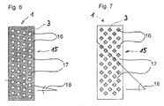
- Fig. 4
- eine Grundmetallisierung, die mittels Siebdruck mit einer Terminierungspaste erzeugt worden ist, mit einer erfindungsgemäßen Struktur aus einzelnen Punkten,
- Fig. 5
- mit einer erfindungsgemäßen Struktur aus einzelnen Linien,
- Fig. 6
- mit einer erfindungsgemäßen netzartigen Struktur und
- Fig. 7
- mit einer erfindungsgemäßen Struktur, die aus einer vollflächig gedruckten Metallisierung durch mechanisches Abtragen herausgearbeitet worden ist.
- Fig. 4
- a basic metallization, which was produced by means of screen printing with a termination paste, with a structure according to the invention from individual points
- Fig. 5
- with a structure of individual lines according to the invention,
- Fig. 6
- with a net-like structure according to the invention and
- Fig. 7
- with a structure according to the invention, which has been worked out from a full-surface printed metallization by mechanical removal.
Der schematische Aufbau der hier eingesetzten Vielschichtaktoren entspricht dem in Figur 1 dargestellten. Die erfindungsgemäßen Außenelektroden unterscheiden sich von der in den Figuren 2 und 3 dargestellten Außenelektrode durch die Strukturierung der Grundmetallisierung.The schematic structure of the multi-layer actuators used here corresponds that shown in Figure 1. The external electrodes according to the invention differ from the outer electrode shown in FIGS. 2 and 3 by structuring the base metallization.
Die erfindungsgemäße Strukturierung der Grundmetallisierung wurde an fünf Ausführungsbeispielen geprüft. Dazu wurden zunächst Grundkörper von Vielschichtaktoren entsprechend Figur 1 hergestellt, auf denen in unterschiedlichen Mustern die Grundmetallisierung aufgebracht wurde. Danach wurden die Außenelektroden der Aktoren vervollständigt.The structuring of the base metallization according to the invention was carried out on five Tested embodiments. For this purpose, basic bodies of Multi-layer actuators manufactured according to Figure 1, on which in different patterns the basic metallization was applied. After that the external electrodes of the actuators were completed.
Die Herstellung von Grundkörpern der Aktoren erfolgt wie nachstehend beschrieben: Aus einem niedrig sinternden piezokeramischen Werkstoff, Bindersystem eine 125 µm dicke Folie präpariert. Auf diese Folie wird eine Innenelektrodenpaste aus Silber-Palladium-Pulver in einem Gewichtsverhältnis von 70/30 und einem geeigneten Bindersystem mittels Siebdruck aufgebracht. Eine Vielzahl derartiger Folien wird gestapelt und zu einem Laminat verpresst. Das Laminat wird in einzelne, stabförmige. Aktoren getrennt, diese werden bei etwa 400 °C pyrolysiert und bei etwa 1100 °C gesintert. Anschließend werden die Aktorgrundkörper an allen Seiten mechanisch bearbeitet.The basic bodies of the actuators are produced as follows described: from a low-sintering piezoceramic material, Binder system prepared a 125 µm thick film. On this slide is a Inner electrode paste made of silver-palladium powder in a weight ratio of 70/30 and a suitable binder system applied by screen printing. A large number of such foils are stacked and pressed into a laminate. The laminate is cut into individual, rod-shaped. Actuators separated, these are at pyrolyzed at about 400 ° C and sintered at about 1100 ° C. Then be the actuator base body machined on all sides.
Die Grundmetallisierung 3, beispielsweise aus einer geeigneten Silber-Palladium-Terminierungspaste,
wird mittels Siebdruck aufgebracht, wobei
dadurch eine Struktur 15 entsteht, dass die bedruckten Flächen 16 von
unbedruckten Flächen 17 unterbrochen sind, wie es in den Figuren 4 bis 6
dargestellt ist. Anschließend erfolgt der Einbrennprozess. Das entstehende
punkt-, linien- oder netzartige Raster 15 aus bedruckten Flächen 16 soll so fein
wie möglich sein, wobei sichergestellt sein muss, dass jeweils benachbarte
Innenelektroden 10, die entsprechend Figur 2 an die Oberfläche des Aktors 1
führen, durch mindestens eine aufgedruckte Fläche 16 miteinander verbunden
werden. Um das zu erreichen ist es sinnvoll, das Raster 15 unter einem Winkel,
in den Figuren 4 bis 6 mit 18 gekennzeichnet, gegenüber der Richtung der
Innenelekroden 10 verlaufen zu lassen. Wird die Struktur zu fein, so sinkt die
Festigkeit des Verbundes zur später aufgebrachten Verstärkungsschicht,
beispielsweise einer aufgelöteten Netzelektrode. Bei einem Abstand der
Innenelektroden 10 von 100 µm hat sich als besonders vorteilhaft ein bedruckter
Bereich 16 der Grundmetallisierung 3 von 0,2 bis 0,3 mm mit gleich großen
Unterbrechungen 17 erwiesen.The
Die Grundmetallisierung kann auch durch örtliches mechanisches Abtragen einer
ganzflächig aufgetragenen Schicht strukturiert werden, beispielsweise durch
Einsägen oder Einritzen. Die Struktur kann weiterhin durch einen
elektrochemischen Prozess erzeugt werden, wobei die Tatsache genutzt wird,
dass elektrochemisch abgeschiedene Metalle porös sind. Eine derart erzeugte
Struktur 15 ist in Figur 7 dargestellt. The base metallization can also be done by local mechanical removal of a
can be structured over the entire surface, for example by
Sawing or scoring. The structure can still be defined by a
electrochemical process are generated, taking advantage of the fact
that electrodeposited metals are porous. One generated in this
Nach dem Einbrennen der Grundmetallisierung werden die Außenelektroden durch die Verstärkungsschicht vervollständigt, beispielsweise durch das Auflöten eines Metalldraht-Netzes. Anschließend können die Aktoren polarisiert und ihre Eigenschaften gemessen werden.After the basic metallization has been burned in, the outer electrodes are removed completed by the reinforcement layer, for example by soldering of a metal wire network. The actuators can then be polarized and their Properties are measured.
Nachstehend werden Proben von vier Ausführungsbeispielen mit erfindungsgemäßen Außenelektroden mit Proben mit Außenelektroden nach dem Stand der Technik verglichen.Below are samples from four embodiments with external electrodes according to the invention with samples with external electrodes compared to the prior art.
Die Aktorgrundkörper der Proben, die entsprechend dem oben beschriebenen Verfahren hergestellt worden sind, haben Abmessungen von 10 x 10 mm2 Grundfläche und 30 mm Höhe. Die Dicke einer Keramikeinzellage beträgt nach dem Sintern 100 µm, die Dicke einer Innenmetallisierungsschicht 2 µm. Die Aktorgrundkörper werden wie folgt weiterbehandelt:The actuator base bodies of the samples, which were produced according to the method described above, have dimensions of 10 x 10 mm 2 base area and 30 mm height. The thickness of a single ceramic layer is 100 µm after sintering, and the thickness of an inner metallization layer is 2 µm. The basic actuator bodies are treated as follows:
Für Aktoren nach dem Stand der Technik als Referenz wird die
Grundmetallisierung 3 aus einer geeigneten AgPd Terminierungspaste mittels
Siebdruck aufgebracht, wobei keine Struktur erzeugt wird. Die Schicht ist
gleichmäßig dick, die Schichtdicke beträgt 8 µm nach dem Einbrennen bei 800
°C.For actuators according to the prior art, the
Für das erste Ausführungsbeispiel wird die Grundmetallisierung 3 aus einer
geeigneten AgPd Terminierungspaste mittels Siebdruck aufgebracht, wobei eine
rasterartige Struktur 15 aus runden Punkten 16 erzeugt wird, vergleichbar dem
Muster in Figur 4. Der Punktdurchmesser beträgt 0,2 mm, der Freiraum 17
zwischen zwei Punkten ebenfalls 0,2 mm. Das Raster 15 ist unter einem Winkel
18 von 20° zur Richtung der Innenelektroden 10 geneigt, so dass jeweils
benachbarte Innenelektroden 10 durch mindestens eine aufgedruckte Fläche 16
miteinander verbunden werden. Die Schicht der Punkte ist gleichmäßig dick, die
Schichtdicke beträgt 9 µm nach dem Einbrennen bei 800 °C. For the first exemplary embodiment, the
Für das zweite Ausführungsbeispiel wird die Grundmetallisierung 3 aus einer
geeigneten AgPd Terminierungspaste mittels Siebdruck aufgebracht, wobei eine
linienartige Struktur 15 erzeugt wird, vergleichbar dem Muster in Figur 5. Die
Breite der Linien 16 beträgt 0,2 mm, der Abstand 17 zwischen zwei Linien beträgt
ebenfalls 0,2 mm. Die Linien 16 sind, wie beim ersten Ausführungsbeispiel, unter
einem Winkel 18 gegenüber der Richtung der Innenelektroden 10 geneigt. Die
Schicht der Linienstruktur 15 ist gleichmäßig dick, die Schichtdicke beträgt 9 µm
nach dem Einbrennen bei 800 °C.For the second exemplary embodiment, the
Für das dritte Ausführungsbeispiel wird die Grundmetallisierung 3 aus einer
geeigneten AgPd Terminierungspaste mittels Siebdruck aufgebracht, wobei
keine Struktur erzeugt wird. Die Schicht ist gleichmäßig dick, die Schichtdicke
beträgt 8 µm nach dem Einbrennen bei 800 °C. In der Grundmetallisierung 3 wird
ein Raster 15 aus Quadraten 16 erzeugt, indem mittels einer Diamantsäge die
Schicht in 0,2 mm große Quadrate 16 aufgetrennt wird, vergleichbar dem Muster
in Figur 7. Der Abstand 17 der Quadrate 16 beträgt 0,1 mm. Die
Verbindungslinien der Quadrate im Raster 15 verlaufen unter einem Winkel 18
von 35° zur Richtung der Innenelektroden, damit jeweils benachbarte
Innenelektroden durch mindestens ein Quadrat überdeckt werden.For the third exemplary embodiment, the
Für das fünfte Ausführungsbeispiel, das hier nicht dargestellt ist, wird die Grundmetallisierung elektrochemisch in Form einer Nickelschicht abgeschieden. Die Nickelschicht ist etwa 2 µm dick und wird von einer ebenfalls elektrochemisch abgeschiedenen, 0,1 µm dicken Goldschicht überdeckt. Die Goldschicht verbessert die Lötfähigkeit und hat keine andere Funktion. Die Nickelschicht ist verfahrensbedingt nicht völlig geschlossen und hat eine feine netzartige Struktur, wobei Durchbrüche in der Größenordnung des Keramikkorns liegen, etwa zwischen 5 und 10 µm.For the fifth embodiment, which is not shown here, the Base metallization deposited electrochemically in the form of a nickel layer. The nickel layer is about 2 µm thick and is also one electrochemically deposited, 0.1 µm thick gold layer covers. The Gold layer improves solderability and has no other function. The The nickel layer is not completely closed due to the process and has a fine layer reticulated structure, with openings in the order of magnitude of the ceramic grain lie between about 5 and 10 microns.
Auf die fünf Ausführungsbeispiele werden anschließend mit einem geeigneten Prozess die Außenelektroden durch ein aufgelötetes Drahtnetz vervollständigt. Als Netzwerkstoff wird ein dem thermischen Ausdehnungskoeffizienten der Keramik vergleichbarer Werkstoff, beispielsweise FeNi36, verwendet. Der Drahtdurchmesser beträgt 100 µm, die Maschenweite 200 µm. Das Netz ist galvanisch vorbehandelt, beispielsweise verkupfert, um die Lötbarkeit zu verbessern. Als Lot wird SnAg4 verwendet. Die Lötzeit beträgt 10 Minuten bei 240 °C.In the five exemplary embodiments, the outer electrodes are then completed by a soldered wire mesh using a suitable process. A material comparable to the thermal expansion coefficient of the ceramic, for example FeNi 36 , is used as the network material. The wire diameter is 100 µm, the mesh size is 200 µm. The network is pre-treated, for example copper-plated, to improve the solderability. SnAg 4 is used as the solder. The soldering time is 10 minutes at 240 ° C.
Nach dem Löten ist optisch erkennbar, dass bei den Varianten 2 bis 5 der
Ausführungsbeispiele das Lot die Innenelektroden auch auf den nicht mit
Grundmetallisierung versehenen Flächen benetzt hat.After soldering, it can be seen that
Die Aktoren werden gereinigt und mit einer geeigneten Lackierung isoliert. Nach dem Anlöten der Anschlussdrähte an die Elektrodennetze werden die Aktoren in Prüfrahmen mit 2000 N vorgespannt und mit einem Trapezsignal angesteuert. Dabei wird die Ansteuerspannung in 100 µs von 0 V auf 200 V angehoben, 1 ms auf 200 V gehalten, und dann in 100 µs auf 0 V erniedrigt. Die Wiederholfrequenz ist 200 Hz. Die Aktoren erreichen dabei Betriebstemperaturen von 150 bis 160 °C.The actuators are cleaned and insulated with a suitable paint. To When the connection wires are soldered to the electrode networks, the actuators in Test frame preloaded with 2000 N and controlled with a trapezoid signal. The control voltage is raised in 100 µs from 0 V to 200 V, 1 ms kept at 200 V, and then decreased to 0 V in 100 µs. The Repetition frequency is 200 Hz. The actuators reach operating temperatures from 150 to 160 ° C.
Die Variante 1 zeigt bereits bei 106 Zyklen eine deutliche und starke Rissbildung. Die Risse durchtrennen die Isolierzone in beliebigen Richtungen, Risse entlang der Innenelektroden sind eher selten.Variant 1 already shows a clear and strong crack formation at 10 6 cycles. The cracks cut through the insulation zone in any direction, cracks along the inner electrodes are rather rare.
Die Varianten 2 und 3 zeigen nahezu identisches Verhalten, das sich von
Variante 1 deutlich unterscheidet. Bei 106 Zyklen tritt eine kaum sichtbare
Rissbildung auf. Bei 107 Zyklen tritt Rissbildung auf. Die Risse verlaufen alle
entlang der Innenelektroden, treten etwa doppelt so häufig auf wie bei der
Variante 1, sind aber deutlich schwächer ausgeprägt. Auch nach 108 Zyklen
bleibt dieser Zustand unverändert.
Die Variante 4 zeigt das günstigste Rissverhalten. Erst ab 108 Zyklen tritt
deutliche Rissbildung auf. Die Risse verlaufen ebenfalls alle entlang der
Innenelektroden. Bei dieser Variante scheren jedoch die Quadrate des Quadrat-Rasters
16 leicht von der Keramik ab. Die Ursache lag darin, dass der Übergang
zwischen Grundmetallisierung und Keramik beim Sägeprozess am Rand der
Quadrate geschädigt wurde. Durch optimieren der Trennschnitte in der
Grundmetallisierung kann eine Beschädigung des Keramikwerkstoffs vermieden
werden. Durch geeignete Ätzverfahren kann eine Beschädigung des
Keramikwerkstoffs ebenfalls vermieden werden.
Die Variante 5 zeigt ein Rissverhalten wie die Varianten 2 und 3, jedoch ist die
Haftfestigkeit des Nickels auf der Keramik nicht ausreichend. Es treten nach und
nach örtlich Ablösungen der Grundmetallisierung von der Keramik auf, wodurch
die Funktion des Aktors bei langen Laufzeiten beeinträchtigt werden kann.The
Claims (26)
Applications Claiming Priority (4)
| Application Number | Priority Date | Filing Date | Title |
|---|---|---|---|
| DE10054735 | 2000-11-06 | ||
| DE10054735 | 2000-11-06 | ||
| DE10152490 | 2001-10-24 | ||
| DE10152490A DE10152490A1 (en) | 2000-11-06 | 2001-10-24 | External electrodes on piezoceramic multilayer actuators |
Publications (3)
| Publication Number | Publication Date |
|---|---|
| EP1204152A2 true EP1204152A2 (en) | 2002-05-08 |
| EP1204152A3 EP1204152A3 (en) | 2004-06-02 |
| EP1204152B1 EP1204152B1 (en) | 2006-05-17 |
Family
ID=26007567
Family Applications (1)
| Application Number | Title | Priority Date | Filing Date |
|---|---|---|---|
| EP01126097A Expired - Lifetime EP1204152B1 (en) | 2000-11-06 | 2001-11-02 | External electrodes for piezoceramic stack actuators |
Country Status (5)
| Country | Link |
|---|---|
| US (1) | US6798123B2 (en) |
| EP (1) | EP1204152B1 (en) |
| JP (1) | JP4338341B2 (en) |
| AT (1) | ATE326769T1 (en) |
| DE (2) | DE10152490A1 (en) |
Cited By (9)
| Publication number | Priority date | Publication date | Assignee | Title |
|---|---|---|---|---|
| WO2003073523A2 (en) * | 2002-02-22 | 2003-09-04 | Epcos Ag | Piezo actuator comprising a structured external electrode |
| WO2003105246A2 (en) * | 2002-06-07 | 2003-12-18 | Pi Ceramic Gmbh Keramische Technologien Und Bauelemente | Method for the production of a monolithic multilayer actuator, monolithic multilayer actuator made of a piezoceramic or electrostrictive material, and external electrical contact for a monolithic multilayer actuator |
| WO2004077583A1 (en) * | 2003-02-24 | 2004-09-10 | Epcos Ag | Electrical multilayered component and layer stack |
| EP1764844A1 (en) * | 2005-09-16 | 2007-03-21 | Delphi Technologies, Inc. | Piezoelectric actuator |
| WO2007118883A1 (en) * | 2006-04-19 | 2007-10-25 | Robert Bosch Gmbh | Piezo actuator and method for the production thereof |
| WO2007118878A1 (en) * | 2006-04-19 | 2007-10-25 | Robert Bosch Gmbh | Piezo actuator comprising externally contacted inner electrodes of a piezo element |
| CN103028538A (en) * | 2012-12-15 | 2013-04-10 | 山东力创科技有限公司 | Built-in polar surface piezoelectric ceramic piece for ultrasonic transducer of ultrasonic heat meter |
| WO2015082399A1 (en) * | 2013-12-04 | 2015-06-11 | Robert Bosch Gmbh | Piezo actuator and control valve with such a piezo actuator |
| EP3291316B1 (en) * | 2016-08-29 | 2021-12-15 | The Boeing Company | Actuator assemblies, mechanical assemblies including the actuator assemblies, and methods of fabricating the same |
Families Citing this family (24)
| Publication number | Priority date | Publication date | Assignee | Title |
|---|---|---|---|---|
| JP4808915B2 (en) * | 2003-09-24 | 2011-11-02 | 京セラ株式会社 | Multilayer piezoelectric element and injection device |
| JPWO2005064700A1 (en) * | 2003-12-26 | 2007-07-26 | 株式会社村田製作所 | Multilayer ceramic electronic components |
| JP4934988B2 (en) * | 2004-07-27 | 2012-05-23 | 株式会社デンソー | Multilayer piezoelectric element and injector using the same |
| DE102005017108A1 (en) * | 2005-01-26 | 2006-07-27 | Epcos Ag | Piezoelectric multi-layer component e.g. piezo-ceramic piezo actuator, has base with dielectric thicknesses and inner electrodes, and contact units of porous material running perpendicularly to electrodes |
| US20070046149A1 (en) * | 2005-08-23 | 2007-03-01 | Zipparo Michael J | Ultrasound probe transducer assembly and production method |
| JP5201646B2 (en) * | 2006-01-13 | 2013-06-05 | 日本碍子株式会社 | Multilayer piezoelectric element |
| JP4936306B2 (en) * | 2006-01-13 | 2012-05-23 | 日本碍子株式会社 | Multilayer piezoelectric element and manufacturing method thereof |
| EP2003707B1 (en) * | 2006-03-31 | 2012-03-14 | Murata Manufacturing Co. Ltd. | Piezoelectric actuator |
| JP4929875B2 (en) * | 2006-06-30 | 2012-05-09 | 株式会社デンソー | Multilayer piezoelectric element |
| CN101687716B (en) * | 2007-04-24 | 2013-11-13 | 陶瓷技术有限责任公司 | Method for producing a metallized component, corresponding component, and a substate for supporting the component during metalization |
| EP2237337B1 (en) * | 2007-12-26 | 2016-03-16 | Kyocera Corporation | Laminated piezoelectric element, and injection device and fuel injection system using the same |
| JP2011510505A (en) * | 2008-01-23 | 2011-03-31 | エプコス アクチエンゲゼルシャフト | Piezoelectric multilayer components |
| EP2232599B1 (en) * | 2008-01-23 | 2014-12-24 | Epcos AG | Piezoelectric multilayer component |
| JP5587793B2 (en) * | 2008-01-23 | 2014-09-10 | エプコス アクチエンゲゼルシャフト | Piezoelectric multilayer components |
| DE102008062021A1 (en) * | 2008-08-18 | 2010-03-04 | Epcos Ag | Piezo actuator in multilayer construction |
| JP5430106B2 (en) * | 2008-09-22 | 2014-02-26 | 京セラ株式会社 | Multilayer piezoelectric element, injection device including the same, and fuel injection system |
| JP5342846B2 (en) * | 2008-10-15 | 2013-11-13 | 京セラ株式会社 | Multilayer piezoelectric element, injection device including the same, and fuel injection system |
| JP2010109057A (en) * | 2008-10-29 | 2010-05-13 | Kyocera Corp | Stacked piezoelectric device, and injection apparatus and fuel injection system equipped with the same |
| DK2359419T3 (en) * | 2008-11-20 | 2013-04-15 | Ceramtec Gmbh | Multilayer actuator with outer electrodes made of a metallic, porous, expandable conductive layer |
| WO2010101056A1 (en) * | 2009-03-04 | 2010-09-10 | 京セラ株式会社 | Laminated piezoelectric element, jetting device provided with same, and fuel jetting system |
| DE102011014446A1 (en) * | 2011-03-18 | 2012-09-20 | Epcos Ag | Monolithic multilayer piezoelectric actuator for actuating injection valve in motor car, has outer electrode including contacted portions that are mechanically and electrically connected with electrode contact layer |
| JP5840997B2 (en) * | 2012-03-30 | 2016-01-06 | 京セラ株式会社 | Multilayer piezoelectric element and piezoelectric actuator, injection device, fuel injection system |
| JP6259092B2 (en) * | 2014-07-22 | 2018-01-10 | 京セラ株式会社 | Multilayer piezoelectric element, injection device including the same, and fuel injection system |
| JP6907493B2 (en) * | 2016-09-28 | 2021-07-21 | ブラザー工業株式会社 | Actuator device, connection structure of wiring members, liquid discharge device, and manufacturing method of actuator device |
Citations (8)
| Publication number | Priority date | Publication date | Assignee | Title |
|---|---|---|---|---|
| US4523121A (en) * | 1982-05-11 | 1985-06-11 | Nec Corporation | Multilayer electrostrictive element which withstands repeated application of pulses |
| DE3940619A1 (en) * | 1989-06-09 | 1990-12-13 | Avx Corp | ELECTROSTRICTIVE ACTUATORS |
| EP0427901A1 (en) * | 1989-11-14 | 1991-05-22 | Battelle Memorial Institute | Method of manufacturing a multilayer piezoelectric actuator stack |
| DE4224284A1 (en) * | 1991-07-25 | 1993-01-28 | Hitachi Metals Ltd | LAMINATE SHIFTING TRANSDUCER ELEMENT AND METHOD FOR THE PRODUCTION THEREOF |
| US5406164A (en) * | 1993-06-10 | 1995-04-11 | Brother Kogyo Kabushiki Kaisha | Multilayer piezoelectric element |
| EP0655790A1 (en) * | 1992-07-08 | 1995-05-31 | Kureha Kagaku Kogyo Kabushiki Kaisha | Piezoelectric device and process for production thereof |
| DE19860001A1 (en) * | 1998-12-23 | 2000-07-06 | Siemens Ag | Piezoelectric component, especially for controlling an internal combustion engine injection valve, has electrically insulating material-containing interspaces between its piezoceramic layers |
| DE19928178A1 (en) * | 1999-06-19 | 2000-08-10 | Bosch Gmbh Robert | Piezoactuator e.g. for valve, has multilayer construction of piezo layers, intermediate electrodes, alternating lateral electrode contacting, and division of multilayer structure into sub-actuators |
Family Cites Families (19)
| Publication number | Priority date | Publication date | Assignee | Title |
|---|---|---|---|---|
| JPS6098691A (en) * | 1983-11-04 | 1985-06-01 | Mitsubishi Rayon Co Ltd | Manufacture of laminated type piezoelectric actuator |
| JPS61283180A (en) * | 1985-06-07 | 1986-12-13 | Murata Mfg Co Ltd | Laminated piezoelectric substance |
| JPS61283182A (en) * | 1985-06-07 | 1986-12-13 | Murata Mfg Co Ltd | Compound piezoelectric substance |
| JPS62151359A (en) * | 1985-12-25 | 1987-07-06 | Alps Electric Co Ltd | Thermal head |
| JPS63142875A (en) * | 1986-12-05 | 1988-06-15 | Sumitomo Special Metals Co Ltd | Piezoelectric laminated actuator |
| US5103557A (en) * | 1988-05-16 | 1992-04-14 | Leedy Glenn J | Making and testing an integrated circuit using high density probe points |
| US5254212A (en) * | 1990-09-13 | 1993-10-19 | Hitachi Metals, Ltd. | Method of fabricating electrostrictive-effect device |
| US5339068A (en) * | 1992-12-18 | 1994-08-16 | Mitsubishi Materials Corp. | Conductive chip-type ceramic element and method of manufacture thereof |
| US5459371A (en) * | 1993-03-12 | 1995-10-17 | Brother Kogyo Kabushiki Kaisha | Multilayer piezoelectric element |
| JPH0758371A (en) * | 1993-08-17 | 1995-03-03 | Brother Ind Ltd | Stacked piezoelectric element |
| JPH07154006A (en) * | 1993-12-01 | 1995-06-16 | Brother Ind Ltd | Multilayer piezoelectric element and fabrication thereof |
| JPH07226541A (en) * | 1994-02-09 | 1995-08-22 | Brother Ind Ltd | Multilayered piezoelectric element |
| JPH07283453A (en) * | 1994-04-12 | 1995-10-27 | Brother Ind Ltd | Laminated piezoelectric element |
| JPH0832131A (en) * | 1994-07-20 | 1996-02-02 | Brother Ind Ltd | Laminated piezolectric element and its manufacture |
| DE19648545B4 (en) * | 1996-11-25 | 2009-05-07 | Ceramtec Ag | Monolithic multilayer actuator with external electrodes |
| DE19715488C1 (en) * | 1997-04-14 | 1998-06-25 | Siemens Ag | Piezoelectric actuator |
| US6183578B1 (en) * | 1998-04-21 | 2001-02-06 | Penn State Research Foundation | Method for manufacture of high frequency ultrasound transducers |
| EP1061591A4 (en) * | 1998-12-18 | 2007-05-02 | Denso Corp | Piezoelectric multilayer body |
| JP2002203999A (en) * | 2000-11-06 | 2002-07-19 | Denso Corp | Laminated type piezoelectric-substance element and the manufacturing method thereof |
-
2001
- 2001-10-24 DE DE10152490A patent/DE10152490A1/en not_active Withdrawn
- 2001-11-01 US US10/016,488 patent/US6798123B2/en not_active Expired - Fee Related
- 2001-11-02 AT AT01126097T patent/ATE326769T1/en not_active IP Right Cessation
- 2001-11-02 DE DE50109803T patent/DE50109803D1/en not_active Expired - Lifetime
- 2001-11-02 EP EP01126097A patent/EP1204152B1/en not_active Expired - Lifetime
- 2001-11-06 JP JP2001341148A patent/JP4338341B2/en not_active Expired - Fee Related
Patent Citations (8)
| Publication number | Priority date | Publication date | Assignee | Title |
|---|---|---|---|---|
| US4523121A (en) * | 1982-05-11 | 1985-06-11 | Nec Corporation | Multilayer electrostrictive element which withstands repeated application of pulses |
| DE3940619A1 (en) * | 1989-06-09 | 1990-12-13 | Avx Corp | ELECTROSTRICTIVE ACTUATORS |
| EP0427901A1 (en) * | 1989-11-14 | 1991-05-22 | Battelle Memorial Institute | Method of manufacturing a multilayer piezoelectric actuator stack |
| DE4224284A1 (en) * | 1991-07-25 | 1993-01-28 | Hitachi Metals Ltd | LAMINATE SHIFTING TRANSDUCER ELEMENT AND METHOD FOR THE PRODUCTION THEREOF |
| EP0655790A1 (en) * | 1992-07-08 | 1995-05-31 | Kureha Kagaku Kogyo Kabushiki Kaisha | Piezoelectric device and process for production thereof |
| US5406164A (en) * | 1993-06-10 | 1995-04-11 | Brother Kogyo Kabushiki Kaisha | Multilayer piezoelectric element |
| DE19860001A1 (en) * | 1998-12-23 | 2000-07-06 | Siemens Ag | Piezoelectric component, especially for controlling an internal combustion engine injection valve, has electrically insulating material-containing interspaces between its piezoceramic layers |
| DE19928178A1 (en) * | 1999-06-19 | 2000-08-10 | Bosch Gmbh Robert | Piezoactuator e.g. for valve, has multilayer construction of piezo layers, intermediate electrodes, alternating lateral electrode contacting, and division of multilayer structure into sub-actuators |
Cited By (18)
| Publication number | Priority date | Publication date | Assignee | Title |
|---|---|---|---|---|
| US7268471B2 (en) | 2002-02-22 | 2007-09-11 | Epcos Ag | Piezo actuator comprising a structured external electrode |
| WO2003073523A3 (en) * | 2002-02-22 | 2004-02-19 | Epcos Ag | Piezo actuator comprising a structured external electrode |
| WO2003073523A2 (en) * | 2002-02-22 | 2003-09-04 | Epcos Ag | Piezo actuator comprising a structured external electrode |
| WO2003105246A2 (en) * | 2002-06-07 | 2003-12-18 | Pi Ceramic Gmbh Keramische Technologien Und Bauelemente | Method for the production of a monolithic multilayer actuator, monolithic multilayer actuator made of a piezoceramic or electrostrictive material, and external electrical contact for a monolithic multilayer actuator |
| WO2003105246A3 (en) * | 2002-06-07 | 2004-06-10 | Pi Ceramic Gmbh Keramische Tec | Method for the production of a monolithic multilayer actuator, monolithic multilayer actuator made of a piezoceramic or electrostrictive material, and external electrical contact for a monolithic multilayer actuator |
| CN100483766C (en) * | 2002-06-07 | 2009-04-29 | Pi陶瓷技术及元件有限公司 | Method for the production of a monolithic multilayer actuator, monolithic multilayer actuator made of a piezoceramics or electrostrictive material, and external electrical contact for a monolithic mul |
| US7449077B2 (en) | 2002-06-07 | 2008-11-11 | Pi Ceramic Gmbh Keramische Technologien Und Bauelemente | Method for the production of monolithic multilayer actuator monolithic multilayer actuator made of a piezoceramic or electrostrictive material and external electrical contact for a monolithic multilayer actuator |
| WO2004077583A1 (en) * | 2003-02-24 | 2004-09-10 | Epcos Ag | Electrical multilayered component and layer stack |
| US7358655B2 (en) | 2003-02-24 | 2008-04-15 | Epcos Ag | Electrical multilayered component and layer stack |
| WO2007031700A1 (en) * | 2005-09-16 | 2007-03-22 | Delphi Technologies, Inc. | Piezoelectric actuator |
| EP1764844A1 (en) * | 2005-09-16 | 2007-03-21 | Delphi Technologies, Inc. | Piezoelectric actuator |
| US8358051B2 (en) | 2005-09-16 | 2013-01-22 | Delphi Technologies Holding S.Arl | Piezoelectric actuator |
| WO2007118883A1 (en) * | 2006-04-19 | 2007-10-25 | Robert Bosch Gmbh | Piezo actuator and method for the production thereof |
| WO2007118878A1 (en) * | 2006-04-19 | 2007-10-25 | Robert Bosch Gmbh | Piezo actuator comprising externally contacted inner electrodes of a piezo element |
| CN103028538A (en) * | 2012-12-15 | 2013-04-10 | 山东力创科技有限公司 | Built-in polar surface piezoelectric ceramic piece for ultrasonic transducer of ultrasonic heat meter |
| WO2015082399A1 (en) * | 2013-12-04 | 2015-06-11 | Robert Bosch Gmbh | Piezo actuator and control valve with such a piezo actuator |
| EP3291316B1 (en) * | 2016-08-29 | 2021-12-15 | The Boeing Company | Actuator assemblies, mechanical assemblies including the actuator assemblies, and methods of fabricating the same |
| US11871673B2 (en) | 2016-08-29 | 2024-01-09 | The Boeing Company | Methods of fabricating actuator assemblies |
Also Published As
| Publication number | Publication date |
|---|---|
| US6798123B2 (en) | 2004-09-28 |
| ATE326769T1 (en) | 2006-06-15 |
| JP4338341B2 (en) | 2009-10-07 |
| DE10152490A1 (en) | 2002-05-08 |
| EP1204152A3 (en) | 2004-06-02 |
| US20020089266A1 (en) | 2002-07-11 |
| DE50109803D1 (en) | 2006-06-22 |
| EP1204152B1 (en) | 2006-05-17 |
| JP2002171004A (en) | 2002-06-14 |
Similar Documents
| Publication | Publication Date | Title |
|---|---|---|
| EP1204152B1 (en) | External electrodes for piezoceramic stack actuators | |
| EP1636859B1 (en) | Piezoelectric component with a predetermined breaking point, method for producing the component and use of the component | |
| EP0958620B1 (en) | Piezo electric actuator with a new type of contacting and a method for the production thereof | |
| EP1597780B1 (en) | Electrical multilayered component and layer stack | |
| EP1512183B1 (en) | Method for the production of a monolithic multilayer actuator, monolithic multilayer actuator made of a piezoceramic or electrostrictive material, and external electrical contact for a monolithic multilayer actuator | |
| EP1908131B1 (en) | Method for producing a monolithic piezo actuator with stack elements, monilithic piezo actuator with stack elements, and use of the piezo actuator | |
| DE10042893A1 (en) | Laminated piezoelectric control element e.g. for optical arrangement, has alternating piezoelectric, inner electrode layers, outer electrodes in sides, top and bottom inactive ceramic layers and insulating blocks | |
| EP1239525B1 (en) | Piezoceramic multilayer actuators and method of manufacturing | |
| EP2359419B1 (en) | Multi-layered actuator with external electrodes made of a metallic, porous, expandable conductive layer | |
| DE102004031404B4 (en) | Piezoelectric component with predetermined breaking point and electrical connection element, method for producing the component and use of the component | |
| EP1476907B1 (en) | Piezo actuator comprising a structured external electrode | |
| EP2011170B1 (en) | Method for the production of a piezo actuator | |
| DE3832658A1 (en) | Laminated adjusting element | |
| WO2008025315A1 (en) | Piezoceramic surface actuator and method for the production thereof | |
| EP2543085B1 (en) | Piezoelectric component | |
| EP2232599B1 (en) | Piezoelectric multilayer component | |
| WO2006077245A1 (en) | Monolithic multilayer actuator and method for the production thereof | |
| WO2013167368A1 (en) | Method for producing a multi-layered structural element, and a multi-layered structural element produced according to said method | |
| DE102011109008A1 (en) | Method for producing a piezoelectric multilayer component | |
| EP4294135A1 (en) | Metallic structure as a precursor for electrical circuits and method of manufacturing an electrical circuit | |
| DE10246784B4 (en) | Acoustic wave device with low insertion loss and method of manufacture | |
| WO2010103127A1 (en) | Piezoactuator of multilayer design and method for fastening an outer electrode in a piezoactuator | |
| DE102004014455A1 (en) | Capacitor comprises substrate with dielectric layers, between which is electrode comprising central active zone and edge zones connected to it by intermediate zones with thin bridging connections, contacts being mounted on edge zones |
Legal Events
| Date | Code | Title | Description |
|---|---|---|---|
| PUAI | Public reference made under article 153(3) epc to a published international application that has entered the european phase |
Free format text: ORIGINAL CODE: 0009012 |
|
| AK | Designated contracting states |
Kind code of ref document: A2 Designated state(s): AT BE CH CY DE DK ES FI FR GB GR IE IT LI LU MC NL PT SE TR |
|
| AX | Request for extension of the european patent |
Free format text: AL;LT;LV;MK;RO;SI |
|
| PUAL | Search report despatched |
Free format text: ORIGINAL CODE: 0009013 |
|
| AK | Designated contracting states |
Kind code of ref document: A3 Designated state(s): AT BE CH CY DE DK ES FI FR GB GR IE IT LI LU MC NL PT SE TR |
|
| AX | Request for extension of the european patent |
Extension state: AL LT LV MK RO SI |
|
| RIC1 | Information provided on ipc code assigned before grant |
Ipc: 7H 01L 41/083 B Ipc: 7H 01L 41/047 A |
|
| 17P | Request for examination filed |
Effective date: 20041202 |
|
| AKX | Designation fees paid |
Designated state(s): AT BE CH CY DE DK ES FI FR GB GR IE IT LI LU MC NL PT SE TR |
|
| 17Q | First examination report despatched |
Effective date: 20050318 |
|
| GRAP | Despatch of communication of intention to grant a patent |
Free format text: ORIGINAL CODE: EPIDOSNIGR1 |
|
| GRAS | Grant fee paid |
Free format text: ORIGINAL CODE: EPIDOSNIGR3 |
|
| GRAA | (expected) grant |
Free format text: ORIGINAL CODE: 0009210 |
|
| AK | Designated contracting states |
Kind code of ref document: B1 Designated state(s): AT BE CH CY DE DK ES FI FR GB GR IE IT LI LU MC NL PT SE TR |
|
| PG25 | Lapsed in a contracting state [announced via postgrant information from national office to epo] |
Ref country code: IE Free format text: LAPSE BECAUSE OF FAILURE TO SUBMIT A TRANSLATION OF THE DESCRIPTION OR TO PAY THE FEE WITHIN THE PRESCRIBED TIME-LIMIT Effective date: 20060517 Ref country code: IT Free format text: LAPSE BECAUSE OF FAILURE TO SUBMIT A TRANSLATION OF THE DESCRIPTION OR TO PAY THE FEE WITHIN THE PRESCRIBED TIME-LIMIT;WARNING: LAPSES OF ITALIAN PATENTS WITH EFFECTIVE DATE BEFORE 2007 MAY HAVE OCCURRED AT ANY TIME BEFORE 2007. THE CORRECT EFFECTIVE DATE MAY BE DIFFERENT FROM THE ONE RECORDED. Effective date: 20060517 Ref country code: NL Free format text: LAPSE BECAUSE OF FAILURE TO SUBMIT A TRANSLATION OF THE DESCRIPTION OR TO PAY THE FEE WITHIN THE PRESCRIBED TIME-LIMIT Effective date: 20060517 Ref country code: FI Free format text: LAPSE BECAUSE OF FAILURE TO SUBMIT A TRANSLATION OF THE DESCRIPTION OR TO PAY THE FEE WITHIN THE PRESCRIBED TIME-LIMIT Effective date: 20060517 Ref country code: GB Free format text: LAPSE BECAUSE OF FAILURE TO SUBMIT A TRANSLATION OF THE DESCRIPTION OR TO PAY THE FEE WITHIN THE PRESCRIBED TIME-LIMIT Effective date: 20060517 |
|
| REG | Reference to a national code |
Ref country code: GB Ref legal event code: FG4D Free format text: NOT ENGLISH |
|
| REG | Reference to a national code |
Ref country code: CH Ref legal event code: EP |
|
| REG | Reference to a national code |
Ref country code: IE Ref legal event code: FG4D Free format text: LANGUAGE OF EP DOCUMENT: GERMAN |
|
| REF | Corresponds to: |
Ref document number: 50109803 Country of ref document: DE Date of ref document: 20060622 Kind code of ref document: P |
|
| PG25 | Lapsed in a contracting state [announced via postgrant information from national office to epo] |
Ref country code: SE Free format text: LAPSE BECAUSE OF FAILURE TO SUBMIT A TRANSLATION OF THE DESCRIPTION OR TO PAY THE FEE WITHIN THE PRESCRIBED TIME-LIMIT Effective date: 20060817 Ref country code: DK Free format text: LAPSE BECAUSE OF FAILURE TO SUBMIT A TRANSLATION OF THE DESCRIPTION OR TO PAY THE FEE WITHIN THE PRESCRIBED TIME-LIMIT Effective date: 20060817 |
|
| PG25 | Lapsed in a contracting state [announced via postgrant information from national office to epo] |
Ref country code: ES Free format text: LAPSE BECAUSE OF FAILURE TO SUBMIT A TRANSLATION OF THE DESCRIPTION OR TO PAY THE FEE WITHIN THE PRESCRIBED TIME-LIMIT Effective date: 20060828 |
|
| PG25 | Lapsed in a contracting state [announced via postgrant information from national office to epo] |
Ref country code: PT Free format text: LAPSE BECAUSE OF FAILURE TO SUBMIT A TRANSLATION OF THE DESCRIPTION OR TO PAY THE FEE WITHIN THE PRESCRIBED TIME-LIMIT Effective date: 20061017 |
|
| NLV1 | Nl: lapsed or annulled due to failure to fulfill the requirements of art. 29p and 29m of the patents act | ||
| PGFP | Annual fee paid to national office [announced via postgrant information from national office to epo] |
Ref country code: AT Payment date: 20061113 Year of fee payment: 6 |
|
| PG25 | Lapsed in a contracting state [announced via postgrant information from national office to epo] |
Ref country code: MC Free format text: LAPSE BECAUSE OF NON-PAYMENT OF DUE FEES Effective date: 20061130 Ref country code: LI Free format text: LAPSE BECAUSE OF NON-PAYMENT OF DUE FEES Effective date: 20061130 Ref country code: BE Free format text: LAPSE BECAUSE OF NON-PAYMENT OF DUE FEES Effective date: 20061130 Ref country code: CH Free format text: LAPSE BECAUSE OF NON-PAYMENT OF DUE FEES Effective date: 20061130 |
|
| GBV | Gb: ep patent (uk) treated as always having been void in accordance with gb section 77(7)/1977 [no translation filed] |
Effective date: 20060517 |
|
| REG | Reference to a national code |
Ref country code: IE Ref legal event code: FD4D |
|
| PLBE | No opposition filed within time limit |
Free format text: ORIGINAL CODE: 0009261 |
|
| STAA | Information on the status of an ep patent application or granted ep patent |
Free format text: STATUS: NO OPPOSITION FILED WITHIN TIME LIMIT |
|
| 26N | No opposition filed |
Effective date: 20070220 |
|
| EN | Fr: translation not filed | ||
| REG | Reference to a national code |
Ref country code: CH Ref legal event code: PL |
|
| BERE | Be: lapsed |
Owner name: CERAMTEC A.G. INNOVATIVE CERAMIC ENGINEERING Effective date: 20061130 |
|
| PG25 | Lapsed in a contracting state [announced via postgrant information from national office to epo] |
Ref country code: FR Free format text: LAPSE BECAUSE OF FAILURE TO SUBMIT A TRANSLATION OF THE DESCRIPTION OR TO PAY THE FEE WITHIN THE PRESCRIBED TIME-LIMIT Effective date: 20070309 Ref country code: GR Free format text: LAPSE BECAUSE OF FAILURE TO SUBMIT A TRANSLATION OF THE DESCRIPTION OR TO PAY THE FEE WITHIN THE PRESCRIBED TIME-LIMIT Effective date: 20060818 |
|
| PG25 | Lapsed in a contracting state [announced via postgrant information from national office to epo] |
Ref country code: TR Free format text: LAPSE BECAUSE OF FAILURE TO SUBMIT A TRANSLATION OF THE DESCRIPTION OR TO PAY THE FEE WITHIN THE PRESCRIBED TIME-LIMIT Effective date: 20060517 Ref country code: LU Free format text: LAPSE BECAUSE OF NON-PAYMENT OF DUE FEES Effective date: 20061102 |
|
| PG25 | Lapsed in a contracting state [announced via postgrant information from national office to epo] |
Ref country code: AT Free format text: LAPSE BECAUSE OF NON-PAYMENT OF DUE FEES Effective date: 20071102 |
|
| PG25 | Lapsed in a contracting state [announced via postgrant information from national office to epo] |
Ref country code: FR Free format text: LAPSE BECAUSE OF FAILURE TO SUBMIT A TRANSLATION OF THE DESCRIPTION OR TO PAY THE FEE WITHIN THE PRESCRIBED TIME-LIMIT Effective date: 20060517 Ref country code: CY Free format text: LAPSE BECAUSE OF FAILURE TO SUBMIT A TRANSLATION OF THE DESCRIPTION OR TO PAY THE FEE WITHIN THE PRESCRIBED TIME-LIMIT Effective date: 20060517 |
|
| REG | Reference to a national code |
Ref country code: DE Ref legal event code: R081 Ref document number: 50109803 Country of ref document: DE Owner name: CERAMTEC GMBH, DE Free format text: FORMER OWNER: CERAMTEC AG, 73207 PLOCHINGEN, DE Effective date: 20110216 |
|
| PGFP | Annual fee paid to national office [announced via postgrant information from national office to epo] |
Ref country code: DE Payment date: 20130131 Year of fee payment: 12 |
|
| REG | Reference to a national code |
Ref country code: DE Ref legal event code: R119 Ref document number: 50109803 Country of ref document: DE Effective date: 20140603 |
|
| PG25 | Lapsed in a contracting state [announced via postgrant information from national office to epo] |
Ref country code: DE Free format text: LAPSE BECAUSE OF NON-PAYMENT OF DUE FEES Effective date: 20140603 |