EP1204948B1 - Secure microcontroller against attacks based on current consumption values - Google Patents
Secure microcontroller against attacks based on current consumption values Download PDFInfo
- Publication number
- EP1204948B1 EP1204948B1 EP00953248A EP00953248A EP1204948B1 EP 1204948 B1 EP1204948 B1 EP 1204948B1 EP 00953248 A EP00953248 A EP 00953248A EP 00953248 A EP00953248 A EP 00953248A EP 1204948 B1 EP1204948 B1 EP 1204948B1
- Authority
- EP
- European Patent Office
- Prior art keywords
- microcontroller
- μce
- cap
- com
- efficient
- Prior art date
- Legal status (The legal status is an assumption and is not a legal conclusion. Google has not performed a legal analysis and makes no representation as to the accuracy of the status listed.)
- Expired - Lifetime
Links
Images


Classifications
-
- H—ELECTRICITY
- H01—ELECTRIC ELEMENTS
- H01L—SEMICONDUCTOR DEVICES NOT COVERED BY CLASS H10
- H01L23/00—Details of semiconductor or other solid state devices
- H01L23/57—Protection from inspection, reverse engineering or tampering
- H01L23/576—Protection from inspection, reverse engineering or tampering using active circuits
-
- G—PHYSICS
- G06—COMPUTING; CALCULATING OR COUNTING
- G06K—GRAPHICAL DATA READING; PRESENTATION OF DATA; RECORD CARRIERS; HANDLING RECORD CARRIERS
- G06K19/00—Record carriers for use with machines and with at least a part designed to carry digital markings
- G06K19/06—Record carriers for use with machines and with at least a part designed to carry digital markings characterised by the kind of the digital marking, e.g. shape, nature, code
- G06K19/067—Record carriers with conductive marks, printed circuits or semiconductor circuit elements, e.g. credit or identity cards also with resonating or responding marks without active components
- G06K19/07—Record carriers with conductive marks, printed circuits or semiconductor circuit elements, e.g. credit or identity cards also with resonating or responding marks without active components with integrated circuit chips
- G06K19/073—Special arrangements for circuits, e.g. for protecting identification code in memory
- G06K19/07309—Means for preventing undesired reading or writing from or onto record carriers
- G06K19/07363—Means for preventing undesired reading or writing from or onto record carriers by preventing analysis of the circuit, e.g. dynamic or static power analysis or current analysis
-
- H—ELECTRICITY
- H01—ELECTRIC ELEMENTS
- H01L—SEMICONDUCTOR DEVICES NOT COVERED BY CLASS H10
- H01L2224/00—Indexing scheme for arrangements for connecting or disconnecting semiconductor or solid-state bodies and methods related thereto as covered by H01L24/00
- H01L2224/01—Means for bonding being attached to, or being formed on, the surface to be connected, e.g. chip-to-package, die-attach, "first-level" interconnects; Manufacturing methods related thereto
- H01L2224/42—Wire connectors; Manufacturing methods related thereto
- H01L2224/47—Structure, shape, material or disposition of the wire connectors after the connecting process
- H01L2224/48—Structure, shape, material or disposition of the wire connectors after the connecting process of an individual wire connector
- H01L2224/4805—Shape
- H01L2224/4809—Loop shape
- H01L2224/48091—Arched
-
- H—ELECTRICITY
- H01—ELECTRIC ELEMENTS
- H01L—SEMICONDUCTOR DEVICES NOT COVERED BY CLASS H10
- H01L2224/00—Indexing scheme for arrangements for connecting or disconnecting semiconductor or solid-state bodies and methods related thereto as covered by H01L24/00
- H01L2224/01—Means for bonding being attached to, or being formed on, the surface to be connected, e.g. chip-to-package, die-attach, "first-level" interconnects; Manufacturing methods related thereto
- H01L2224/42—Wire connectors; Manufacturing methods related thereto
- H01L2224/47—Structure, shape, material or disposition of the wire connectors after the connecting process
- H01L2224/48—Structure, shape, material or disposition of the wire connectors after the connecting process of an individual wire connector
- H01L2224/481—Disposition
- H01L2224/48151—Connecting between a semiconductor or solid-state body and an item not being a semiconductor or solid-state body, e.g. chip-to-substrate, chip-to-passive
- H01L2224/48221—Connecting between a semiconductor or solid-state body and an item not being a semiconductor or solid-state body, e.g. chip-to-substrate, chip-to-passive the body and the item being stacked
- H01L2224/48225—Connecting between a semiconductor or solid-state body and an item not being a semiconductor or solid-state body, e.g. chip-to-substrate, chip-to-passive the body and the item being stacked the item being non-metallic, e.g. insulating substrate with or without metallisation
- H01L2224/48227—Connecting between a semiconductor or solid-state body and an item not being a semiconductor or solid-state body, e.g. chip-to-substrate, chip-to-passive the body and the item being stacked the item being non-metallic, e.g. insulating substrate with or without metallisation connecting the wire to a bond pad of the item
- H01L2224/48228—Connecting between a semiconductor or solid-state body and an item not being a semiconductor or solid-state body, e.g. chip-to-substrate, chip-to-passive the body and the item being stacked the item being non-metallic, e.g. insulating substrate with or without metallisation connecting the wire to a bond pad of the item the bond pad being disposed in a recess of the surface of the item
Definitions
- the invention relates to microcontrollers intended to be embedded in portable objects and, in particular, in such map-sized objects more commonly referred to as smart cards.
- Smart cards are generally used in applications in which security of storage and data processing confidential are essential. They are intended in particular for applications in the field of health, to television applications toll, or even banking applications for example electronic purse.
- Micro-controllers are programmed automatic controllers in the form of an integrated circuit. They apply a sequence of instructions logical data to data from their internal memories or from from the outside world, via an input / output pad.
- micro-smart card controllers are designed in CMOS technology. This technology makes it possible to integrate same circuit, subsets useful for the operation of the microcontroller, that is to say in particular a central processing unit CPU, non-volatile non-rewritable memories and read-only ROM (Read Only Memory), non-volatile memory Rewritable type Flash.
- EEPROM Electrically Erasable Programmable Read Only Memory
- FRAM Feromagnetic Random Access Memory
- volatile memory RAM Random Access Memory
- Fraudsters have developed so-called current attacks in order to to obtain confidential data managed by the micro-controller and for example keys intended for the implementation of algorithms of encryption implemented in micro-controllers such as algorithms known as DES (Data Encryption Standard) or RSA (Rivest Shamir Adelman).
- DES Data Encryption Standard
- RSA Raster Shamir Adelman
- the fraudsters connect in particular a resistor R of low value, in particular of 1 ⁇ , in series between a voltage supply source V ⁇ C of the microcontroller and its power supply pad VCC . They then display the variations of the voltage R Icc (t) as a function of time obtained in response to the execution of several hundreds or even thousands of instructions applied to identical, similar or different operands by means of a coupled computer. for example, to a digital oscilloscope that amplifies these variations, they sample and digitize the results obtained for a non-real-time analysis.
- US Pat. No. 4,932,053 relates to security confidential information contained in an integrated circuit.
- a circuit of protection is used. This protection circuit makes it possible to activate the simulation, according to a pseudo-random sequence generated by a generators, current consumption values identical to those real memory cells.
- US Pat. No. 4,827,451 relates to the field of memories constructed as a matrix of memory cells. Said cells, being accessible by the rows and columns, are connected to read and write circuits that are used to program them according to two states - "1" or "0" according to the data of inputs - and read the state thus programmed.
- the memory cells are type requiring a programming current in order to be programmed at "1” and does not require any current when programming at "0".
- Said security circuit consists of a simulation circuit activating when programming to "0" to deliver a current identical to the one delivered by a memory cell during a "1" programming.
- a technical problem proposes to solve the invention is to secure a portable object of the type smart card.
- the present invention is as defined in the reventications whose preambles are constituted by the characteristics described in US 4,932,053 and US 4,827,451.
- the means for varying the supply voltage of the effective data processing part comprise: a variable resistance as a function of time connected in series with the supply pad of the microcontroller, this variable resistor being for example an open switch during time intervals T off and closed during time intervals T on , the duty cycle T off / (T on + T off ) varying as a function of time, the period T on + T off varying in function of time.
- the means for varying the supply voltage of the effective part of data processing include advantageously a pulse generator, this generator of pulses comprising a synchronization circuit of crossing of voltage threshold across the effective part of data processing.
- the means for varying the supply voltage of the effective part of data processing furthermore comprise advantageously a capacitor, this capacitor being for example a capacity with a capacity greater than 0.1 nanofarad.
- the microcontroller comprises a main layer of silicon whose active face, which incorporates a circuit and carries the contact pads, is sealed to a complementary layer of protection by means of a sealing layer, the means for varying the tension feeding of the effective part of data processing being located in the complementary protective layer.
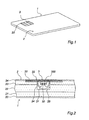
- an object portable device is in the form of a card 1 substantially parallelepipedal rectangular and thin one of which body 2 incorporates an electronic module 3.
- the card body 2 consists of five sheets 20, 21, 22, 23 and 24 laminated plastics and has a cavity 25 for the incorporation of module 3.
- the module 3 comprises a microcontroller 30 whose pads 300 electrically connected by means of wires 31 conductors, to flush contact pads 32 on the surface of the card body 2. These beaches 32 are based on a thickness 33 of a dielectric epoxy glass type.
- the microcontroller assembly 30 and wires 31 conductors is embedded in a protective resin 34.
- the microcontroller 30 is in the form of a rectangular parallelepiped whose thickness is of the order of 180 ⁇ m and whose surface is of the order of 10 mm 2 .
- This microcontroller 30 comprises a main layer 301 of silicon whose active face, which integrates a circuit and carries the studs 300 contact is sealed to a complementary layer 302 of protection of silicon by means of a sealing layer 303.
- This layer complementary 302 is provided with openings 304 located in line with pads 300 to allow their connection to the ranges 32.
- the pads 300 are five in number. These are VCC, RST, CLK, I / O and GND pads respectively connected to the tracks contact module VCC, RST, CLK, I / O and GND.
- VCC power supply is intended to power the microcontroller.
- the plot RST is intended for transmitting a delivery signal Zero to the microcontroller
- the clock pad CLK is intended for the transmission of a clock signal to the microcontroller
- the pad input / output I / O is intended to allow data exchange between the micro-controller and the outside world
- the plot of grounding GND allows the grounding of the microcontroller.
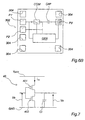
- the integrated circuit of the microcontroller 30 according to the invention has different active parts. These include a part microcontroller interface ⁇ CI and an effective part of treatment of ⁇ CE data shown in Figure 5.
- the micro-controller interface part or micro-interface controller ⁇ CI advantageously comprises only means which consume energy that is not likely to reveal information as to the confidential data processed by the microcontroller.
- the micro-controller interface ⁇ CI includes example a charge pump or interface circuits associated with RST, CLK and I / O pads. With regard to the RST plot, this is including means for detecting an initialization signal and associated means of initialization of the microcontroller. With regard to concerning the CLK pad, it is a means of detecting frequencies between a low limit and a high limit. Finally, with regard to concerning the I / O pad, these are means intended to allow the microcontroller communicate from an input mode to an output mode or vice versa.
- the effective part of data processing or micro-controller effective ⁇ CE is a part of the microcontroller 30 which includes subsets whose inverters are intended for the treatment of confidential data. It is therefore part of the microcontroller likely to give fraudsters information about these confidential data.
- it includes the central unit CPU processing, possibly a cryptoprocessor associated with this unit, data bus and address control circuits as well as RAM, ROM and EEPROM memories or any memories of a Another type.
- the microcontroller 30 also comprises a GEN pulse generator, CAP capacitor and switch COM.
- the pulse generator, the capacity and the switch are means for varying the supply voltage of the microcontroller effective.
- the GEN pulse generator is for example formed of two oscillators consisting, for each of them, of an inverter with hysteresis of Schmitt type on the input circuit, a capacitor connected between the input of the invertor and the ground and a resistor connected between the output of this inverter and its input, said two oscillators being coupled together by a resistor to form a modulated frequency signal source.
- the pulse generator GEN advantageously comprises a synchronization circuit crossing a threshold voltage V threshold of the voltage V ⁇ CE at the terminals of the effective microcontroller.
- This circuit may be formed of a voltage comparator whose positive input is connected to a reference voltage, the threshold voltage V, whose negative input is connected to the voltage at the terminals of the efficient microcontroller, and whose output is connected to the input D of a flip-flop synchronized by the synchronization signal from the modulated frequency signal source.
- CAP capacity has a capacity greater than about 0.1 nanofarad, in particular between about 1 nanofarad and about 10 nanofarads, for example of the order of 6 nanofarads.
- the electrodes with a capacity of 1.5 nanofarad have a surface of the order of 1 mm 2 .
- a capacity of 6 nanofarads has a surface of the order of 4mm 2 .
- the switch COM can be, in the invention, replaced by a variable resistance as a function of time connected in series with the VCC power supply pad of the micro-controller.
- the I / O, RST and CLK pads are connected by electrical connection lines to the microcontroller ⁇ CI interface.
- the GND pad is connected via electrical connection lines to the GEN pulse generator, the CAP capacitor, the efficient ⁇ CE microcontroller and the ⁇ CI microcontroller interface.
- the VCC pad is connected by electrical connection lines to the GEN pulse generator, the COM switch and the ⁇ CI interface microcontroller.
- the COM switch is connected by electrical connection lines to the GEN pulse generator and the CAP capacitor.
- an electrical connection line connects the effective micro-controller ⁇ CE to the electrical connection line connecting the capacitor CAP to the switch COM and an electrical connection line connects the GEN generator to the latter line so as to allow monitoring of the voltage V ⁇ CE for its comparison with the voltage V threshold .
- microcontroller of the type shown in FIG. said elements are arranged in the manner shown in Figs. 6A and 6B in which the complementary layer 302 (FIG. 6B) comprises GEN pulse generator, CAP capacitor and switch COM, and the main layer 301 ( Figure 6A), which carries the pads of contact, includes micro-controller effective parts ⁇ CE and micro-controller ⁇ CI interface.
- the complementary layer 302 comprises GEN pulse generator, CAP capacitor and switch COM
- main layer 301 Figure 6A
- Figure 6A which carries the pads of contact
- the main layer 301 comprises three studs interconnection P1, P2 and P3, a first pad P1 connected to the VCC pad, a second pad P2 connected to the effective microcontroller and a third P3 pad connected to the GND pad.
- the complementary layer 302 comprises three studs interconnection P1 ', P2' and P3 'intended to be placed in the microcontroller, in the vertical view of the studs P1, P2 and P3, respectively.
- the first pad P1 ' is connected, on the one hand, to COM switch and, on the other hand, to the GEN pulse generator, the second pad P2 'is connected to the common point between the switch COM and the capacitance CAP and the third pad P3 'is connected, on the one hand, CAP and the GEN pulse generator.
- the pads P1, P2 and P3 are respectively electrically connected to the pads P1 ', P2' and P3 ' via conductive bosses.
- micro-controller presented above does not constitute that an embodiment according to the invention and it is quite possible to provide other embodiments of micro-controllers do not not showing a layered structure but a structure more classic in which the various elements mentioned above: contact, micro-controllers interface and efficient, capacity, generator pulses and switch, are integrated in a single layer of silicon substrate not covered with a complementary layer.
- the energy Ec ⁇ CI consumed by the microcontroller interface is not indicative of the instructions executed by the microcontroller 30 and therefore not revealing the confidential data involved in the execution of said instructions.
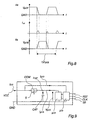
- the elementary gates of the efficient microcontroller are inverters 40 as shown in FIG. 7. These inverters 40 are formed of a P-type transistor 401 connected in series with an N-type transistor 402. The transistor P is brought to FIG. the voltage V ⁇ CE and the transistor N is grounded GND. A capacitor C i is associated with each inverter 40. This capacitance C i is the capacitance equivalent to the physical capacitances of the interconnection lines of the inverter and to the capacitances of the gates forming the transistors P and N of the inverter possibly connected downstream. of the inverter of Figure 7.
- the transistors P and N are controlled by a common control signal V e corresponding to the input voltage of the inverter.
- V e GND
- FIG. 8 shows the variations of the control signal V e , of the intensity of the supply current i cc and of the output signal V s as a function of time t, in the case where the working frequency of the inverter is equal to F ⁇ CE , which is in general the frequency of the clock imposed by the terminal via the pad CLK, but which may be a particular frequency, in the case where the microcontroller is provided with means for generating a clock internal.
- E cc is less than 20% of E d and E s is much smaller than E d .
- the energy E c consumed by the inverter i is mainly dynamic and it is estimated that E c is substantially equal to E d .
- the energy consumed by the efficient microcontroller therefore varies with the square of its supply voltage V ⁇ CE .
- the energy Ec M consumed by the means of the invention is equal to the energy Ec GEN consumed by the pulse generator GEN added to the energy Ec COM consumed by the switch COM and energy Ec CAP consumed by CAP capacity.
- Ec M Ec GEN + Ec COM + Ec CAP
- the energy Ec GEN consumed by the pulse generator GEN is of the same type as the energy consumed by the microcontroller interface. Indeed, it reveals no indication of the confidential data involved in the execution of the instructions.
- the EC COM energy consumed by the COM switch is in fact the energy dissipated by this switch when the capacitor CAP is charging.
- Ec COM Ec CAP during his charge.
- the Ec CAP energy consumed by the CAP capacitor depends on the open or closed state of the COM switch.
- the open or closed state of the switch COM is controlled by the pulse generator GEN. Indeed, this generator is able to send a control signal S to open or close the COM switch. Depending on the signal S received, this switch is closed or open. It is closed during time intervals T on . It is open during time intervals T off.
- a fraudster has access only to the intensity of the supply current of the microcontroller as a whole and consequently only to the energy consumed by the micro-controller as a whole.
- Ec ⁇ CI reveals no information on the switching of the inverters of the effective microcontroller and consequently no information on the confidential data processed. Also, thanks to the invention, the fraudster will not be able to access said data during time intervals T off .
- the energy consumed by the microcontroller is equal to the energy consumed by the microcontroller interface, added to the energy consumed by the means according to the invention and added to the energy consumed by the effective microcontroller.
- Ec C ⁇ Ec .mu.Ci + Ec ⁇ CE + Ec M .
- INS instruction applied to the same OPE operands and executed by the microcontroller according to the invention.
- this INS statement is executed on some clock transitions. AT each clock transition, part of the INS instruction is executed and some of the N inverters of the efficient microcontroller are the subject a change of state for this purpose.
- the energy consumed by the efficient microcontroller during such a transition is directly proportional to the square of the voltage V ⁇ CE at the terminals of said microcontroller.
- the voltage V ⁇ CE at the terminals of the efficient microcontroller is the same as the voltage V CAP across the capacitors CAP. Also, the voltage at the terminals of the efficient microcontroller varies constantly.
- the difference between the energies consumed by the efficient microcontroller is all the greater as they are functions of the square of the supply voltage V ⁇ CE of this microcontroller.
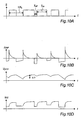
- FIGS. 10A to 10D respectively display the signal S, the current I CAP of the supply current of the capacitor CAP, the voltage V ⁇ CE of the supply of the efficient microcontroller and the intensity of the current Icc of the microphone supply. -controller as a function of time t.
- the cyclic ratio T off / (T on + T off ) thus varies over time and, advantageously, randomly and therefore unpredictable for the fraudster.
- T s due to the manner in which the pulse generator is produced, comprising two oscillators coupled with a Schmitt-type inverter.
- the current I CAP of the capacitor CAP power is positive during the time intervals T on during which the capacitor is charged.
- the capacity is at maximum load when the switch goes to the open state.
- the intensity of the current I CAP is negative in the time intervals T off during which the capacitance is discharged to supply the effective microcontroller.
- the supply voltage V ⁇ CE of the efficient microcontroller increases in the time intervals T on and decreases in the time intervals T off .
- ⁇ V represents the depth of modulation of the voltage across the capacitor.
- the intensity Icc of the supply current of the microcontroller is equal to I ⁇ CI in T off and then increases in T on , where it is equal to I ⁇ CI + I CAP + I ⁇ CE .
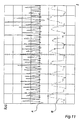
- FIG. 11 shows the variations of the intensity of the current Icc as a function of time t, on the one hand, in the case of a microcontroller according to the state of the art (signature A) and, on the other hand , in the case of the same microcontroller according to the invention (signature B) for the execution of identical instructions applied to the same operands.
- signature A the state of the art
- signature B the same microcontroller according to the invention
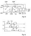
- capacitor CAP1 is discharged to a reference voltage, for example GND, through switch COM3 while switches COM1 and COM2 are open, before being recharged through switch COM1 while the switches COM2 and COM3 are open.
- the CAP1 capacitor once charged through the switch COM1, discharges into the capacitor CAP2 in parallel with the efficient microcontroller ⁇ CE through the switch COM2 while the switches COM1 and COM2 are open.
- FIG. 13 the course of the signals S 1 , S 2 and S 3 has been shown in time.
- the embodiment makes it possible to consume a constant energy independent of the activity of the ⁇ CE. It is no longer possible to obtain confidential information by analyzing the current Icc. This embodiment increases the energy consumption of the efficient microcontroller.
Abstract
Description
L'invention concerne des micro-contrôleurs destinés à être incorporés dans des objets portatifs et, en particulier, dans de tels objets au format carte plus communément appelés cartes à puce.The invention relates to microcontrollers intended to be embedded in portable objects and, in particular, in such map-sized objects more commonly referred to as smart cards.
Les cartes à puce sont en général utilisées dans des applications dans lesquelles la sécurité du stockage et du traitement de données confidentielles sont essentielles. Elles sont notamment destinées à des applications du domaine de la santé, à des applications de la télévision à péage, ou encore, à des applications bancaires par exemple dites de porte-monnaie électronique.Smart cards are generally used in applications in which security of storage and data processing confidential are essential. They are intended in particular for applications in the field of health, to television applications toll, or even banking applications for example electronic purse.
Les micro-contrôleurs sont des automates programmés réalisés sous forme de circuit intégré. Ils appliquent une suite d'instructions logiques aux données issues de leurs mémoires internes ou provenant du monde extérieur, par l'intermédiaire d'un plot d'entrée/sortie.Micro-controllers are programmed automatic controllers in the form of an integrated circuit. They apply a sequence of instructions logical data to data from their internal memories or from from the outside world, via an input / output pad.
Habituellement, les micro-contrôleurs de cartes à puce sont conçus en technologie CMOS. Cette technologie permet d'intégrer, dans un même circuit, des sous-ensembles utiles au fonctionnement du micro-contrôleur, c'est-à-dire notamment une unité centrale de traitement CPU, des mémoires non volatiles non réinscriptibles et en lecture seule de type ROM (Read Only Memory), des mémoires non volatiles réinscriptibles de type Flash. EEPROM (Electrically Erasable Programmable Read Only Memory) ou FRAM (Ferromagnetic Random Access Memory) et des mémoires volatiles RAM (Random Access Memory).Usually, micro-smart card controllers are designed in CMOS technology. This technology makes it possible to integrate same circuit, subsets useful for the operation of the microcontroller, that is to say in particular a central processing unit CPU, non-volatile non-rewritable memories and read-only ROM (Read Only Memory), non-volatile memory Rewritable type Flash. EEPROM (Electrically Erasable Programmable Read Only Memory) or FRAM (Ferromagnetic Random Access Memory) and volatile memory RAM (Random Access Memory).
Des fraudeurs ont développés des attaques dites en courant en vue d'obtenir des données confidentielles gérées par le micro-contrôleur et par exemple des clés destinées à la mise en oeuvre d'algorithmes de cryptage implementés dans les micro-contrôleurs tels que les algorithmes connus sous les noms de DES (Data Encryption Standard) ou de RSA (Rivest Shamir Adelman).Fraudsters have developed so-called current attacks in order to to obtain confidential data managed by the micro-controller and for example keys intended for the implementation of algorithms of encryption implemented in micro-controllers such as algorithms known as DES (Data Encryption Standard) or RSA (Rivest Shamir Adelman).
Ces attaques sont basées sur le principe suivant lequel l'énergie
EcµC consommée par un micro-contrôleur exécutant, dans un intervalle
de temps T, une instruction INS appliquée à des opérandes OPE, est
toujours la même et constitue une signature. Autrement dit :
On notera que, dans la relation ci-dessus, ainsi que dans les relations qui suivront dans la présente description, le signe "=" signifie "sensiblement égal".It should be noted that in the above relationship, as well as in the relations which will follow in the present description, the sign "=" means "substantially equal".
Pour la mise en oeuvre des attaques en courant, les fraudeurs connectent notamment une résistance R de faible valeur, notamment d' 1 Ω, en série entre une source d'alimentation en tension VµC du micro-contrôleur et son plot d'alimentation VCC. Ils visualisent alors les variations de la tension R Icc(t) en fonction du temps obtenues en réponse à l'exécution de plusieurs centaines voire plusieurs milliers d'instructions appliquées à des opérandes identiques, semblables ou différentes au moyen d'un ordinateur couplé, par exemple, à un oscilloscope numérique qui amplifient ces variations, les échantillonnent et numérisent les résultats obtenus en vue d'une analyse en temps différé.For the implementation of current attacks, the fraudsters connect in particular a resistor R of low value, in particular of 1 Ω, in series between a voltage supply source V μC of the microcontroller and its power supply pad VCC . They then display the variations of the voltage R Icc (t) as a function of time obtained in response to the execution of several hundreds or even thousands of instructions applied to identical, similar or different operands by means of a coupled computer. for example, to a digital oscilloscope that amplifies these variations, they sample and digitize the results obtained for a non-real-time analysis.
De telles attaques, qui ont la particularité d'être non destructives, sont redoutables.Such attacks, which have the distinction of being non-destructive, are formidable.
C'est la raison pour laquelle les fabricants de micro-contrôleurs et les fabricants de cartes ont développé des procédés destinés à sécuriser les micro-contrôleurs contre ces attaques.This is the reason why manufacturers of micro-controllers and card manufacturers have developed processes to secure the micro-controllers against these attacks.
La plupart de ces procédés proposent d'utiliser des programmes qui font intervenir un déclenchement d'opérations à des moments pseudo-aléatoires ou font intervenir des opérations qui génèrent un bruit riche en informations aléatoires ou erronées au cours de l'exécution des instructions par le micro-contrôleur.Most of these methods propose using programs that involve triggering operations at times pseudo-random or involve operations that generate a noise rich in random or erroneous information during the execution of instructions by the microcontroller.
Ces procédés montrent cependant de multiples inconvénients. Le temps d'exécution des programmes est long. L'espace mémoire qu'ils occupent est important. Enfin, les données confidentielles ne sont finalement pas protégées contre une analyse approfondie réalisée par les fraudeurs puisque la signature électrique, qui résulte de l'exécution des instructions, est toujours présente.These methods, however, show multiple disadvantages. The run time of programs is long. The memory space they occupy is important. Finally, confidential data are not finally not protected against a thorough analysis by fraudsters since the electrical signature, which results from the execution instructions, is always present.
Un autre procédé, décrit dans la demande de brevet français enregistrée sous le numéro 98 01305, et non rendue publique à la date de priorité de la présente demande, propose de filtrer le courant par une cellule de filtrage passe-bas. Ce procédé permet uniquement d'atténuer les signatures électriques et leur analyse précise permet en définitive d'accéder à certaines données confidentielles.Another method, described in the French patent application registered under number 98 01305, and not made public on the date priority of the present application, proposes to filter the current by a low-pass filter cell. This process only serves to attenuate electrical signatures and their precise analysis ultimately allows to access certain confidential data.
Le brevet US 4 932 053 concerne quant à lui, la sécurité d'informations confidentielles contenues dans un circuit intégré. Dans un certain nombre d'applications concernant des circuits intégrés et plus particulièrement dans des applications du type carte à puce, il est nécessaire d'interdire l'accès de certaines données confidentielles contenues dans la mémoire du circuit à des personnes non autorisées. Afin d'empêcher le fraudeur de procéder à un examen de la consommation en courant aux extrémités du circuit intégré lors d'une opération de lecture ou d'écriture dans la mémoire, un circuit de protection est utilisé. Ce circuit de protection permet d'activer la simulation, selon une séquence pseudo-aléatoire générée par un générateur, de valeurs de consommation en courant identiques à celles des cellules mémoires réelles. US Pat. No. 4,932,053 relates to security confidential information contained in an integrated circuit. In a number of applications concerning integrated circuits and more particularly in smart card type applications, it is necessary to prohibit access to certain confidential data contained in the circuit memory to unauthorized persons. To prevent the fraudster from conducting a review of the current consumption at the ends of the integrated circuit during a reading or writing operation in the memory, a circuit of protection is used. This protection circuit makes it possible to activate the simulation, according to a pseudo-random sequence generated by a generators, current consumption values identical to those real memory cells.
Notons enfin que le brevet US 4 827451 concerne le domaine des mémoires construites sous forme d'une matrice de cellules mémoires. Lesdites cellules, étant accessibles par les lignes et les colonnes , sont connectées à des circuits de lecture et d'écriture qui sont utilisés pour les programmer selon deux états - "1" ou "0" selon les données d'entrées - et lire l'état ainsi programmé. Les cellules mémoires sont du type nécessitant un courant de programmation afin d'être programmées à "1" et ne nécessitant aucun courant lors de la programmation à "0". Ledit circuit de sécurité consiste en un circuit de simulation s'activant lors d'une programmation à "0" pour délivrer un courant identique à celui délivré par une cellule mémoire lors d'une programmation à "1".Finally, note that US Pat. No. 4,827,451 relates to the field of memories constructed as a matrix of memory cells. Said cells, being accessible by the rows and columns, are connected to read and write circuits that are used to program them according to two states - "1" or "0" according to the data of inputs - and read the state thus programmed. The memory cells are type requiring a programming current in order to be programmed at "1" and does not require any current when programming at "0". Said security circuit consists of a simulation circuit activating when programming to "0" to deliver a current identical to the one delivered by a memory cell during a "1" programming.
Compte tenu de ce qui précède, un problème technique que se propose de résoudre l'invention est de sécuriser un objet portatif du type carte à puce.In view of the above, a technical problem proposes to solve the invention is to secure a portable object of the type smart card.
La présente invention est telle que définie dans les reventications dont les préambules sont constitués par les caractéristiques décrites dans US 4 932 053 et US 4 827 451. The present invention is as defined in the reventications whose preambles are constituted by the characteristics described in US 4,932,053 and US 4,827,451.
Etant donné que la consommation en énergie de ladite partie efficace de traitement de données peut être estimée comme étant directement proportionnelle au carré de sa tension d'alimentation, une variation de cette tension bouleverse les signatures électriques et rend leur analyse difficile voire impossible.Since the energy consumption of this part efficient data processing can be estimated as being directly proportional to the square of its supply voltage, a variation of this voltage upsets the electrical signatures and makes their analysis difficult or impossible.
De manière avantageuse, les moyens pour faire varier la tension d'alimentation de la partie efficace de traitement de données comprennent : - une résistance variable en fonction du temps connectée en série avec le plot d'alimentation du micro-contrôleur, cette résistance variable étant par exemple un commutateur ouvert pendant des intervalles de temps Toff et fermé pendant des intervalles de temps Ton, le rapport cyclique Toff/(Ton + Toff) variant en fonction du temps, la période Ton + Toff variant en fonction du temps.Advantageously, the means for varying the supply voltage of the effective data processing part comprise: a variable resistance as a function of time connected in series with the supply pad of the microcontroller, this variable resistor being for example an open switch during time intervals T off and closed during time intervals T on , the duty cycle T off / (T on + T off ) varying as a function of time, the period T on + T off varying in function of time.
Par ailleurs, les moyens pour faire varier la tension d'alimentation de la partie efficace de traitement de données comprennent avantageusement un générateur d'impulsions, ce générateur d'impulsions comprenant un circuit de synchronisation de franchissement de seuil de tension aux bornes de la partie efficace de traitement de données.Moreover, the means for varying the supply voltage of the effective part of data processing include advantageously a pulse generator, this generator of pulses comprising a synchronization circuit of crossing of voltage threshold across the effective part of data processing.
Enfin, les moyens pour faire varier la tension d'alimentation de la partie efficace de traitement de données comprennent en outre avantageusement un condensateur, ce condensateur étant par exemple une capacité dont la capacité est supérieure à 0,1 nanofarad.Finally, the means for varying the supply voltage of the effective part of data processing furthermore comprise advantageously a capacitor, this capacitor being for example a capacity with a capacity greater than 0.1 nanofarad.
Dans certains modes de réalisation avantageux de l'invention le micro-contrôleur comporte une couche principale de silicium dont la face active, qui intègre un circuit et porte les plots de contact, est scellée à une couche complémentaire de protection au moyen d'une couche de scellement, les moyens pour faire varier la tension d'alimentation de la partie efficace de traitement des données étant situés dans la couche complémentaire de protection. In some advantageous embodiments of the invention the microcontroller comprises a main layer of silicon whose active face, which incorporates a circuit and carries the contact pads, is sealed to a complementary layer of protection by means of a sealing layer, the means for varying the tension feeding of the effective part of data processing being located in the complementary protective layer.
L'invention sera mieux comprise à la lecture de l'exposé non limitatif qui suit, rédigé au regard des dessins annexés, dans lesquels :
- la figure 1 montre, en perspective, une carte à puce selon l'invention ;
- la figure 2 montre, en coupe transversale, une carte à puce selon l'invention ;
- la figure 3 montre, en vue de face, les plages de contact d'une carte à puce selon l'invention ;
- la figure 4 montre, en perspective, un micro-contrôleur selon l'invention ;
- la figure 5 schématise les différentes parties constitutives d'un micro-contrôleur selon l'invention ;
- la figure 6A représente la couche active du micro-contrôleur selon l'invention montré à la figure 4 ;
- la figure 6B représente la couche complémentaire du micro-contrôleur selon l'invention montré à la figure 4 ;
- la figure 7 schématise un inverseur CMOS d'une partie efficace de traitement des données d'un micro-contrôleur selon l'invention ;
- la figure 8 montre les variations du signal Ve de commande, de l'intensité icc d'alimentation et du signal Vs de sortie de l'inverseur CMOS de la figure 7 en fonction du temps ;
- la figure 9 est un schéma électrique d'un micro-contrôleur selon l'invention ;
- les figures 10A à 10D montrent, respectivement, les variations du signal S, de l'intensité du courant ICAP, de la tension VµCE et de l'intensité Icc du courant d'alimentation d'un micro-contrôleur selon l'invention en fonction du temps ;
- la figure 11 est un enregistrement comparatif des variations de l'intensité Icc du courant en fonction du temps dans le cas d'un micro-contrôleur selon l'état de la technique (signature A) puis dans le cas d'un micro-contrôleur sécurisé selon l'invention (signature B) ;
- la figure 12 est un schéma électrique d'un mode de réalisation particulier d'un micro-contrôleur selon l'invention ; et
- la figure 13 montre les variations des signaux S1, S2 et S3 en fonction du temps, dans le cas d'un micro-contrôleur correspondant au mode de réalisation de la figure 12.
- Figure 1 shows, in perspective, a smart card according to the invention;
- Figure 2 shows, in cross section, a smart card according to the invention;
- Figure 3 shows, in front view, the contact pads of a smart card according to the invention;
- FIG. 4 shows, in perspective, a microcontroller according to the invention;
- FIG. 5 schematizes the different constituent parts of a microcontroller according to the invention;
- FIG. 6A represents the active layer of the microcontroller according to the invention shown in FIG. 4;
- FIG. 6B represents the complementary layer of the microcontroller according to the invention shown in FIG. 4;
- FIG. 7 schematizes a CMOS inverter of an effective data processing part of a microcontroller according to the invention;
- FIG. 8 shows the variations of the control signal V e , of the power supply i cc and of the output signal V s of the CMOS inverter of FIG. 7 as a function of time;
- Figure 9 is an electrical diagram of a microcontroller according to the invention;
- FIGS. 10A to 10D show, respectively, the variations of the signal S, the intensity of the current I CAP , the voltage V μCE and the intensity Icc of the supply current of a microcontroller according to the invention according to time;
- FIG. 11 is a comparative record of the variations of the intensity Icc of the current as a function of time in the case of a microcontroller according to the state of the art (signature A) then in the case of a microcontroller secure according to the invention (signature B);
- Figure 12 is an electrical diagram of a particular embodiment of a microcontroller according to the invention; and
- FIG. 13 shows the variations of the signals S 1 , S 2 and S 3 as a function of time, in the case of a microcontroller corresponding to the embodiment of FIG. 12.
Dans le mode de réalisation montré aux figures 1, 2 et 3, un objet
portatif selon l'invention se présente sous la forme d'une carte 1
sensiblement parallélépipèdique rectangle et de faible épaisseur dont un
corps 2 intègre un module 3 électronique.In the embodiment shown in FIGS. 1, 2 and 3, an object
portable device according to the invention is in the form of a
Le corps 2 de carte est par exemple constitué de cinq feuilles 20,
21, 22, 23 et 24 plastiques laminées et comporte une cavité 25 pour
l'incorporation du module 3.For example, the
Le module 3 comprend un micro-contrôleur 30 dont des plots 300
de contact sont connectés électriquement, au moyen de fils 31
conducteurs, à des plages 32 de contact affleurantes à la surface du
corps 2 de carte. Ces plages 32 reposent sur une épaisseur 33 d'un
diélectrique du type verre époxy. L'ensemble micro-contrôleur 30 et fils
31 conducteurs est enrobé dans une résine 34 protectrice.The
Dans le mode de réalisation de la figure 4, le micro-contrôleur 30
se présente sous la forme d'un parallélépipède rectangle dont
l'épaisseur est de l'ordre de 180 µm et dont la surface est de l'ordre de
10 mm2.In the embodiment of FIG. 4, the
Ce micro-contrôleur 30 comporte une couche principale 301 de
silicium dont la face active, qui intègre un circuit et porte les plots 300
de contact, est scellée à une couche complémentaire 302 de protection
de silicium au moyen d'une couche de scellement 303. Cette couche
complémentaire 302 est munie d'ouvertures 304 situées à l'aplomb des
plots 300 en vue de permettre leur connexion aux plages 32.This
En pratique, les plots 300 sont au nombre de cinq. Il s'agit des
plots VCC, RST, CLK, I/O et GND respectivement connectés aux plages
de contact VCC, RST, CLK, I/O et GND du module 3. Le plot
d'alimentation VCC est destiné à alimenter le micro-contrôleur. Le plot
de remise à zéro RST est destiné à la transmission d'un signal de remise
à zéro au micro-contrôleur, le plot d'horloge CLK est destiné à la
transmission d'un signal d'horloge au micro-contrôleur, le plot
d'entrée/sortie I/O est destiné à permettre les échanges de données
logiques entre le micro-contrôleur et le monde extérieur et le plot de
mise à la masse GND permet la mise à la masse du micro-contrôleur.In practice, the
Le circuit intégré du micro-contrôleur 30 selon l'invention
comporte différentes parties actives. Il s'agit notamment d'une partie
micro-contrôleur interface µCI et d'une partie efficace de traitement des
données µCE montrées à la figure 5.The integrated circuit of the
La partie micro-contrôleur interface ou micro-contrôleur interface µCI comporte avantageusement uniquement des moyens qui consomment une énergie qui n'est pas susceptible de révéler des informations quant aux données confidentielles traitées par le micro-contrôleur. En pratique, le micro-contrôleur interface µCI comprend par exemple une pompe de charge ou des circuits d'interface associés aux plots RST, CLK et I/O. En ce qui concerne le plot RST, il s'agit notamment de moyens de détection d'un signal d'initialisation et de moyens associés d'initialisation du micro-contrôleur. En ce qui concerne le plot CLK, il s'agit de moyens de détection de fréquences comprises entre une limite basse et une limite haute. Enfin, en ce qui concerne le plot I/O, il s'agit de moyens destinés à permettre au micro-contrôleur communiquer en passant d'un mode entrée à un mode sortie ou réciproquement.The micro-controller interface part or micro-interface controller μCI advantageously comprises only means which consume energy that is not likely to reveal information as to the confidential data processed by the microcontroller. In practice, the micro-controller interface μCI includes example a charge pump or interface circuits associated with RST, CLK and I / O pads. With regard to the RST plot, this is including means for detecting an initialization signal and associated means of initialization of the microcontroller. With regard to concerning the CLK pad, it is a means of detecting frequencies between a low limit and a high limit. Finally, with regard to concerning the I / O pad, these are means intended to allow the microcontroller communicate from an input mode to an output mode or vice versa.
La partie efficace de traitement des données ou micro-contrôleur
efficace µCE est une partie du micro-contrôleur 30 qui comprend des
sous-ensembles dont des inverseurs sont destinés au traitement des
données confidentielles. Elle constitue de ce fait la partie du micro-contrôleur
susceptible de donner aux fraudeurs, des informations sur
ces données confidentielles. En pratique, elle comporte l'unité centrale
de traitement CPU, éventuellement un cryptoprocesseur associé à cette
unité, des circuits de commandes des bus de données et d'adresses
ainsi que les mémoires RAM, ROM et EEPROM ou toutes mémoires d'un
autre type.The effective part of data processing or micro-controller
effective μCE is a part of the
Le micro-contrôleur 30 selon l'invention comprend par ailleurs un
générateur d'impulsions GEN, une capacité CAP et un commutateur
COM. Le générateur d'impulsions, la capacité et le commutateur sont
des moyens pour faire varier la tension d'alimentation du micro-contrôleur
efficace.The
Le générateur d'impulsions GEN est par exemple formé de deux oscillateurs constitués, pour chacun d'entre eux, d'un inverseur avec hystérésis de type Schmitt sur le circuit d'entrée, d'une capacité connectée entre l'entrée de l'inverseur et la masse et d'une résistance connectée entre la sortie de cet inverseur et son entrée, lesdits deux oscillateurs étant couplés entre eux par une résistance pour constituer une source de signal à fréquence modulée. En outre, le générateur d'impulsions GEN comprend avantageusement un circuit de synchronisation de franchissement d'une tension de seuil Vseuil de la tension VµCE aux bornes du micro-contrôleur efficace. Ce circuit peut être formé d'un comparateur de tension dont l'entrée positive est reliée à une tension de référence, la tension Vseuil, dont l'entrée négative est connectée à la tension aux bornes du micro-contrôleur efficace, et dont la sortie est reliée à l'entrée D d'une bascule synchronisée par le signal de synchronisation issu de la source de signal à fréquence modulée.The GEN pulse generator is for example formed of two oscillators consisting, for each of them, of an inverter with hysteresis of Schmitt type on the input circuit, a capacitor connected between the input of the invertor and the ground and a resistor connected between the output of this inverter and its input, said two oscillators being coupled together by a resistor to form a modulated frequency signal source. In addition, the pulse generator GEN advantageously comprises a synchronization circuit crossing a threshold voltage V threshold of the voltage VμCE at the terminals of the effective microcontroller. This circuit may be formed of a voltage comparator whose positive input is connected to a reference voltage, the threshold voltage V, whose negative input is connected to the voltage at the terminals of the efficient microcontroller, and whose output is connected to the input D of a flip-flop synchronized by the synchronization signal from the modulated frequency signal source.
La capacité CAP a une capacité supérieure à environ 0,1 nanofarad, notamment comprise entre environ 1 nanofarad et environ 10 nanofarads, par exemple de l'ordre de 6 nanofarads. On notera que les électrodes d'une capacité de 1,5 nanofarad ont une surface de l'ordre de 1 mm2. Aussi, une capacité de 6 nanofarads a une surface de l'ordre de 4mm2.CAP capacity has a capacity greater than about 0.1 nanofarad, in particular between about 1 nanofarad and about 10 nanofarads, for example of the order of 6 nanofarads. Note that the electrodes with a capacity of 1.5 nanofarad have a surface of the order of 1 mm 2 . Also, a capacity of 6 nanofarads has a surface of the order of 4mm 2 .
Le commutateur COM peut être, dans l'invention, remplacé par une résistance variable en fonction du temps connecté en série avec le plot VCC d'alimentation du micro-contrôleur.The switch COM can be, in the invention, replaced by a variable resistance as a function of time connected in series with the VCC power supply pad of the micro-controller.
Dans l'invention, les plots I / O, RST et CLK sont connectés, par des lignes de connexion électrique, au micro-contrôleur interface µCI. Le plot GND est connecté, par des lignes de connexion électrique, au générateur d'impulsions GEN, à la capacité CAP, au micro-contrôleur efficace µCE et au micro-contrôleur interface µCI. D'autre part, le plot VCC est connecté, par des lignes de connexion électrique, au générateur d'impulsions GEN, au commutateur COM et au micro-contrôleur interface µCI. Par ailleurs, le commutateur COM est connecté, par des lignes de connexion électrique, au générateur d'impulsions GEN et à la capacité CAP. Enfin, une ligne de connexion électrique relie le micro-contrôleur efficace µCE à la ligne de connexion électrique reliant la capacité CAP au commutateur COM et une ligne de connexion électrique relie le générateur GEN à cette dernière ligne de manière à permettre la surveillance de la tension VµCE pour sa comparaison avec la tension Vseuil.In the invention, the I / O, RST and CLK pads are connected by electrical connection lines to the microcontroller μCI interface. The GND pad is connected via electrical connection lines to the GEN pulse generator, the CAP capacitor, the efficient μCE microcontroller and the μCI microcontroller interface. On the other hand, the VCC pad is connected by electrical connection lines to the GEN pulse generator, the COM switch and the μCI interface microcontroller. Furthermore, the COM switch is connected by electrical connection lines to the GEN pulse generator and the CAP capacitor. Finally, an electrical connection line connects the effective micro-controller μCE to the electrical connection line connecting the capacitor CAP to the switch COM and an electrical connection line connects the GEN generator to the latter line so as to allow monitoring of the voltage V μCE for its comparison with the voltage V threshold .
Dans le cas d'un micro-contrôleur du type de la figure 4, les éléments précités sont arrangés à la manière représentée aux figures 6A et 6B dans laquelle la couche complémentaire 302 (figure 6B) comprend le générateur d'impulsions GEN, la capacité CAP et le commutateur COM, et la couche principale 301 (figure 6A), qui porte les plots de contact, comprend les parties micro-contrôleur efficace µCE et micro-contrôleur interface µCI.In the case of a microcontroller of the type shown in FIG. said elements are arranged in the manner shown in Figs. 6A and 6B in which the complementary layer 302 (FIG. 6B) comprises GEN pulse generator, CAP capacitor and switch COM, and the main layer 301 (Figure 6A), which carries the pads of contact, includes micro-controller effective parts μCE and micro-controller μCI interface.
En outre, la couche principale 301 comprend trois plots
d'interconnexion P1, P2 et P3, un premier plot P1 connecté au plot VCC,
un second plot P2 connecté au micro-contrôleur efficace et un troisième
plot P3 connecté au plot GND.In addition, the
De même, la couche complémentaire 302 comprend trois plots
d'interconnexion P1', P2' et P3' destinés à venir se placer, dans le micro-contrôleur,
au regard et à la verticale des plots P1, P2 et P3,
respectivement. Le premier plot P1' est connecté, d'une part, au
commutateur COM et, d'autre part, au générateur d'impulsions GEN, le
second plot P2' est connecté au point commun entre le commutateur
COM et la capacité CAP et le troisième plot P3' est connecté, d'une part,
à la capacité CAP et, d'autre part, au générateur d'impulsions GEN.Similarly, the
Dans le micro-contrôleur 30 de la figure 4, les plots P1, P2 et P3
sont respectivement électriquement connectés aux plots P1', P2' et P3'
par l'intermédiaire de bossages conducteurs.In the
Bien entendu, le micro-contrôleur présenté ci-dessus ne constitue qu'un mode de réalisation selon l'invention et il est tout à fait possible de prévoir d'autres modes de réalisation de micro-contrôleurs ne montrant pas une structure en plusieurs couches mais une structure plus classique dans laquelle les différents éléments précités : plots de contact, micro-contrôleurs interface et efficace, capacité, générateur d'impulsions et commutateur, sont intégrés dans une mono-couche de substrat silicium non recouverte d'une couche complémentaire.Of course, the micro-controller presented above does not constitute that an embodiment according to the invention and it is quite possible to provide other embodiments of micro-controllers do not not showing a layered structure but a structure more classic in which the various elements mentioned above: contact, micro-controllers interface and efficient, capacity, generator pulses and switch, are integrated in a single layer of silicon substrate not covered with a complementary layer.
L'énergie EcµC consommée par un micro-contrôleur selon
l'invention est égale à la somme des énergies EcµCI, EcµCE et EcM
consommées respectivement par le micro-contrôleur interface, le micro-contrôleur
efficace et l'ensemble générateur d'impulsions/capacité/com
mutateur. On a donc la relation :
L'énergie EcµCI consommée par le micro-contrôleur interface n'est
pas révélatrice des instructions exécutées par le micro-contrôleur 30 et
par suite pas révélatrice des données confidentielles mises en jeu dans
l'exécution desdites instructions.The energy Ec μCI consumed by the microcontroller interface is not indicative of the instructions executed by the
Les portes élémentaires du micro-contrôleur efficace sont des
inverseurs 40 tels que montrés à la figure 7. Ces inverseurs 40 sont
formés d'un transistor 401 de type P connecté en série avec un
transistor 402 de type N. Le transistor P est porté à la tension VµCE et le
transistor N est mis à la masse GND. Une capacité Ci est associée à
chaque inverseur 40. Cette capacité Ci est la capacité équivalente aux
capacités physiques des lignes d'interconnexion de l'inverseur et aux
capacités des grilles formant les transistors P et N de l'inverseur
éventuellement connecté en aval de l'inverseur de la figure 7.The elementary gates of the efficient microcontroller are
D'un point de vue fonctionnel, les transistors P et N sont
commandés par un signal de commande commun Ve correspondant à la
tension en entrée de l'inverseur. Lorsque ce signal transporte un 0
logique (Ve = GND), le transistor P est passant et le transistor N est
bloqué de sorte que l'on obtienne un 1 logique en sortie (Vs = VµCE) et
que la capacité Ci se charge. Par contre, lorsque ce signal transporte un
1 logique (Ve = VµCE), le transistor P est bloqué et le transistor N est
passant de sorte que l'on obtienne un 0 logique en sortie (Vs = GND) et
que la capacité Ci se décharge.From a functional point of view, the transistors P and N are controlled by a common control signal V e corresponding to the input voltage of the inverter. When this signal carries a logic 0 (V e = GND), the transistor P is on and the transistor N is off so that a
La figure 8 montre les variations du signal de commande Ve, de l'intensité du courant d'alimentation icc et du signal de sortie Vs en fonction du temps t, dans le cas où la fréquence de travail de l'inverseur est égale à FµCE, qui est en général la fréquence de l'horloge imposée par le terminal via le plot CLK, mais qui peut être une fréquence particulière, dans le cas où le micro-contrôleur est pourvu de moyens de génération d'une horloge interne.FIG. 8 shows the variations of the control signal V e , of the intensity of the supply current i cc and of the output signal V s as a function of time t, in the case where the working frequency of the inverter is equal to F μCE , which is in general the frequency of the clock imposed by the terminal via the pad CLK, but which may be a particular frequency, in the case where the microcontroller is provided with means for generating a clock internal.
Lorsque la tension Ve est constante, les transistors P et N sont
bloqués et l'inverseur 40 est parcouru par un courant de fuite non
visible à la figure 8 dont la valeur moyenne est If sur une période
1/FµCE. L'énergie dissipée, ou énergie statique Es, est alors égale à :
Lorsque la tension Ve varie de manière que le signal à l'entrée de l'inverseur passe d'un 1 logique à un 0 logique ou réciproquement, l'intensité du courant icc varie à la manière indiquée à la figure 8.When the voltage V e varies so that the signal at the input of the inverter changes from a logical 1 to a logical 0 or vice versa, the intensity of the current i cc varies as shown in FIG. 8.
L'inverseur consomme une énergie de court circuit Ecc, qui est
égale à :
De surcroít, lorsque la tension Ve varie de manière que le signal à
l'entrée de l'inverseur passe d'un 1 logique à un 0 logique, la capacité Ci
se charge jusqu'à atteindre la valeur de tension VµCE et l'énergie
dynamique Ed alors consommée est égale à la somme de l'énergie
emmagasinée dans la capacité Ci sous forme d'énergie électrostatique et
de l'énergie dissipée dans la résistance équivalente de limitation du
courant de charge, ici le transistor de type P, soit :
Enfin, lorsque la tension Ve varie de manière que le signal à l'entrée
de l'inverseur passe d'un 0 logique à un 1 logique, la capacité Ci se
décharge au travers du transistor N en dissipant l'énergie
préalablement emmagasinée et égale à 1/2 Ci V2 µCE.Finally, when the voltage V e varies so that the signal at the input of the inverter goes from a logical 0 to a
Pour un inverseur réalisé en technologie CMOS, Ecc est inférieure à 20 % de Ed et Es est très inférieure à Ed. Aussi, l'énergie Ec consommée par l'inverseur i est principalement dynamique et on estime que Ec est sensiblement égale à Ed.For an inverter made in CMOS technology, E cc is less than 20% of E d and E s is much smaller than E d . Also, the energy E c consumed by the inverter i is mainly dynamic and it is estimated that E c is substantially equal to E d .
Aussi, l'énergie consommée par le micro-contrôleur efficace sur
une transition d'horloge est, lorsque ledit micro-contrôleur efficace est
alimenté par la tension VµCE, sensiblement égale à :
![]()
![]()
L'énergie consommée par le micro-contrôleur efficace varie donc avec le carré de sa tension d'alimentation VµCE.The energy consumed by the efficient microcontroller therefore varies with the square of its supply voltage V μCE .
L'énergie EcM consommée par les moyens de l'invention est égale à
l'énergie EcGEN consommée par le générateur d'impulsions GEN
additionnée à l'énergie EcCOM consommée par le commutateur COM et à
l'énergie EcCAP consommée par la capacité CAP. Aussi :
L'énergie EcGEN consommée par le générateur d'impulsions GEN est du même type que l'énergie consommée par le micro-contrôleur interface. En effet, elle ne révèle aucune indication sur les données confidentielles mises en jeu dans l'exécution des instructions.The energy Ec GEN consumed by the pulse generator GEN is of the same type as the energy consumed by the microcontroller interface. Indeed, it reveals no indication of the confidential data involved in the execution of the instructions.
L'énergie EcCOM consommée par le commutateur COM est en fait
l'énergie dissipée par ce commutateur lorsque la capacité CAP se
charge. Aussi :
L'énergie EcCAP consommée par la capacité CAP dépend de l'état ouvert ou fermé du commutateur COM. L'état ouvert ou fermé du commutateur COM est commandé par le générateur d'impulsions GEN. En effet, ce générateur est apte à envoyer un signal S de commande d'ouverture ou de fermeture du commutateur COM. Selon le signal S reçu, ce commutateur est fermé ou ouvert. Il est fermé pendant des intervalles de temps Ton. Il est ouvert pendant des intervalles de temps Toff.The Ec CAP energy consumed by the CAP capacitor depends on the open or closed state of the COM switch. The open or closed state of the switch COM is controlled by the pulse generator GEN. Indeed, this generator is able to send a control signal S to open or close the COM switch. Depending on the signal S received, this switch is closed or open. It is closed during time intervals T on . It is open during time intervals T off.
Dans l'intervalle de temps Toff la capacité se décharge et l'énergie
qu'elle consomme est égale à EcCAP(Toff) telle que :
Dans l'intervalle de temps Ton, la capacité, alimentée par le courant
d'intensité Icc, se charge, et son énergie consommé EcCAP (Ton) est égale
à :
Un fraudeur n'a accès qu'à l'intensité du courant d'alimentation du micro-contrôleur dans son ensemble et par suite qu'à l'énergie consommée par le micro-contrôleur dans son ensemble.A fraudster has access only to the intensity of the supply current of the microcontroller as a whole and consequently only to the energy consumed by the micro-controller as a whole.
Dans l'intervalle de temps Toff, l'énergie consommée par le micro-contrôleur
est égale à l'énergie consommée par le micro-contrôleur
interface. En effet, le micro-contrôleur efficace est alimenté par la
capacité CAP qui se décharge. Aussi, dans Toff :
Or, ainsi que cela a été vu plus haut, EcµCI ne révèle aucune information sur le basculement des inverseurs du micro-contrôleur efficace et par suite aucune information sur les données confidentielles traitées. Aussi, grâce à l'invention, le fraudeur ne pourra pas avoir accès auxdites données pendant les intervalles de temps Toff.However, as has been seen above, Ec μCI reveals no information on the switching of the inverters of the effective microcontroller and consequently no information on the confidential data processed. Also, thanks to the invention, the fraudster will not be able to access said data during time intervals T off .
Par contre, dans l'intervalle de temps Ton, l'énergie consommée par
le micro-contrôleur est égale à l'énergie consommée par le micro-contrôleur
interface, additionnée à l'énergie consommée par les moyens
selon l'invention et additionnée à l'énergie consommée par le micro-contrôleur
efficace. Aussi :
Soit une instruction INS appliquée sur les mêmes opérandes OPE et exécutée par le micro-contrôleur selon l'invention. En pratique, cette instruction INS est exécutée sur quelques transitions d'horloge. A chaque transition d'horloge, une partie de l'instruction INS est exécutée et certains des N inverseurs du micro-contrôleur efficace font l'objet d'un changement d'état à cet effet.An INS instruction applied to the same OPE operands and executed by the microcontroller according to the invention. In practice, this INS statement is executed on some clock transitions. AT each clock transition, part of the INS instruction is executed and some of the N inverters of the efficient microcontroller are the subject a change of state for this purpose.
L'énergie consommée par le micro-contrôleur efficace au cours d'une telle transition est directement proportionnelle au carré de la tension VµCE aux bornes dudit micro-contrôleur.The energy consumed by the efficient microcontroller during such a transition is directly proportional to the square of the voltage V μCE at the terminals of said microcontroller.
Comme la capacité CAP est connectée en parallèle avec le micro-contrôleur efficace, la tension VµCE aux bornes du micro-contrôleur efficace est la même que la tension VCAP aux bornes de la capacité CAP. Aussi, la tension aux bornes du micro-contrôleur efficace varie constamment.As the capacitance CAP is connected in parallel with the efficient microcontroller, the voltage V μCE at the terminals of the efficient microcontroller is the same as the voltage V CAP across the capacitors CAP. Also, the voltage at the terminals of the efficient microcontroller varies constantly.
C'est la raison pour laquelle l'énergie consommée pour l'exécution d'une partie d'instruction INS et, a fortiori, pour une instruction INS, n'est pas toujours la même.This is the reason why the energy consumed for the execution of an INS instruction part and, a fortiori, for an INS instruction, is not always the same.
En fait, dans le cas d'instructions identiques appliquées aux mêmes opérandes, la différence entre les énergies consommées par le micro-contrôleur efficace est d'autant plus grande qu'elles sont fonctions du carré de la tension d'alimentation VµCE de ce micro-contrôleur.In fact, in the case of identical instructions applied to the same operands, the difference between the energies consumed by the efficient microcontroller is all the greater as they are functions of the square of the supply voltage V μCE of this microcontroller.
Il résulte de ce qui précède que le principe cité dans le préambule de la présente description selon lequel EcµC (T ; INS ; OPE) = constante n'est plus vrai dans l'invention et le fraudeur ne pourra donc pas accéder aux informations confidentielles. It follows from the foregoing that the principle mentioned in the preamble of the present description according to which Ec μC (T, INS, OPE) = constant is no longer true in the invention and the fraudster will therefore not be able to access the confidential information. .
Les figures 10A à 10D visualisent respectivement le signal S, l'intensité ICAP du courant d'alimentation de la capacité CAP, la tension VµCE d'alimentation du micro-contrôleur efficace et l'intensité du courant Icc d'alimentation du micro-contrôleur en fonction du temps t.FIGS. 10A to 10D respectively display the signal S, the current I CAP of the supply current of the capacitor CAP, the voltage V μCE of the supply of the efficient microcontroller and the intensity of the current Icc of the microphone supply. -controller as a function of time t.
Ainsi que cela est montré à la figure 10A, les intervalles de temps Toff et Ton varient d'une période Ts = Toff + Ton à une autre. Le rapport cyclique Toff/(Ton + Toff) varie donc au cours du temps et, avantageusement, de manière aléatoire et par suite imprévisible pour le fraudeur. En outre, étant donné que la fermeture du commutateur COM n'est pas réalisée à l'instant précis où la tension aux bornes de la capacité atteint la valeur seuil Vseuil mais au premier coup d'horloge suivant cet instant, et que l'intervalle de temps entre ledit instant et ce premier coup d'horloge est variable, la valeur de Ts = 1/Fs varie de manière aléatoire. Aux variations de Ts décrites ci-avant, s'ajoutent des variations de Ts dues à la manière dont est réalisée le générateur d'impulsions, comprenant deux oscillateurs couplés avec inverseur de type Schmitt.As shown in FIG. 10A, the time intervals T off and T on vary from one period T s = T off + T on to another. The cyclic ratio T off / (T on + T off ) thus varies over time and, advantageously, randomly and therefore unpredictable for the fraudster. In addition, since the closing of the switch COM is not performed at the precise instant when the voltage across the capacitor reaches the threshold value V threshold but at the first clock stroke following this moment, and that the time interval between said instant and this first clock stroke is variable, the value of T s = 1 / F s varies randomly. In addition to the variations of T s described above, there are variations of T s due to the manner in which the pulse generator is produced, comprising two oscillators coupled with a Schmitt-type inverter.
D'autre part, ainsi que cela est montré à la figure 10B, l'intensité du courant ICAP d'alimentation de la capacité CAP est positive durant les intervalles de temps Ton au cours desquels la capacité se charge. Par contre, ICAP décroít dans ces intervalles jusqu'à ce que ICAP(t) = 0. De ce fait, la capacité est en charge maximale au moment où le commutateur passe à l'état ouvert. Par ailleurs, l'intensité du courant ICAP est négative dans les intervalles de temps Toff au cours desquels la capacité se décharge pour alimenter le micro-contrôleur efficace.On the other hand, as shown in FIG 10B, the current I CAP of the capacitor CAP power is positive during the time intervals T on during which the capacitor is charged. On the other hand, I CAP decreases in these intervals until I CAP (t) = 0. As a result, the capacity is at maximum load when the switch goes to the open state. On the other hand, the intensity of the current I CAP is negative in the time intervals T off during which the capacitance is discharged to supply the effective microcontroller.
Ainsi que cela est montré à la figure 10C, la tension d'alimentation VµCE du micro-contrôleur efficace croít dans les intervalles de temps Ton et décroít dans les intervalles de temps Toff. ΔV représente la profondeur de la modulation de la tension aux bornes de la capacité. As shown in FIG. 10C, the supply voltage V μCE of the efficient microcontroller increases in the time intervals T on and decreases in the time intervals T off . ΔV represents the depth of modulation of the voltage across the capacitor.
Enfin, ainsi que cela est montré à la figure 10D, l'intensité Icc du courant d'alimentation du micro-contrôleur est égale à IµCI dans Toff puis augmente dans Ton, où elle est égale à IµCI + ICAP + IµCE.Finally, as shown in FIG. 10D, the intensity Icc of the supply current of the microcontroller is equal to I μCI in T off and then increases in T on , where it is equal to I μCI + I CAP + I μCE .
La figure 11 montre les variations de l'intensité du courant Icc en fonction du temps t, d'une part, dans le cas d'un micro-contrôleur selon l'état de la technique (signature A) et, d'autre part, dans le cas d'un même micro-contrôleur selon l'invention (signature B) pour l'exécution d'instructions identiques appliquées sur des mêmes opérandes. Bien que l'exécution de ces instructions se déroule de la même manière dans le temps, les courbes sont totalement différentes. Les pics d'intensité visibles sur la première courbe ne le sont plus sur la seconde courbe. Les intervalles de temps Toff et Ton apparaissent clairement sur la seconde courbe. Il est ainsi particulièrement difficile de déterminer quoi que ce soit concernant les données confidentielles à partir de la seconde courbe.FIG. 11 shows the variations of the intensity of the current Icc as a function of time t, on the one hand, in the case of a microcontroller according to the state of the art (signature A) and, on the other hand , in the case of the same microcontroller according to the invention (signature B) for the execution of identical instructions applied to the same operands. Although the execution of these instructions takes place in the same way in time, the curves are totally different. The intensity peaks visible on the first curve are no longer on the second curve. The time intervals T off and T on appear clearly on the second curve. It is thus particularly difficult to determine anything about the confidential data from the second curve.
Bien entendu, la description du mode de réalisation de l'invention exposé ci-dessus n'est nullement limitative de l'invention qui doit se comprendre de manière large. D'autres modes de réalisation plus complexes sont susceptibles de donner des résultats particulièrement intéressants. Il s'agit par exemple du mode de réalisation présenté à la figure 12 montrant un micro-contrôleur muni de deux capacités CAP1 et CAP2, trois commutateurs COM1, COM2 et COM3 et trois signaux S1, S2 et S3 de commande de l'ouverture et de la fermeture des trois commutateurs COM1, COM2 et COM3, respectivement. Dans ce mode de réalisation, la capacité CAP1 est déchargée à une tension de référence, par exemple GND, au travers du commutateur COM3 alors que les commutateurs COM1 et COM2 sont ouverts, avant d'être rechargée au travers du commutateur COM1 alors que les commutateurs COM2 et COM3 sont ouverts. La capacité CAP1, une fois chargée au travers du commutateur COM1, se décharge dans la capacité CAP2 en parallèle avec le micro-contrôleur efficace µCE au travers du commutateur COM2 alors que les commutateurs COM1 et COM2 sont ouverts. A la figure 13, on a montré le déroulement des signaux S1, S2 et S3 dans le temps. Le mode de réalisation permet de consommer une énergie constante indépendante de l'activité du µCE. Il n'est plus possible d'obtenir des informations confidentielles en analysant le courant Icc. Ce mode de réalisation augmente la consommation énergétique du micro-contrôleur efficace.Of course, the description of the embodiment of the invention set out above is in no way limiting of the invention which must be understood in a broad manner. Other more complex embodiments are likely to give particularly interesting results. This is for example the embodiment shown in FIG. 12 showing a microcontroller equipped with two capacitors CAP1 and CAP2, three switches COM1, COM2 and COM3 and three signals S1, S2 and S3 controlling the opening and closing the three switches COM1, COM2 and COM3, respectively. In this embodiment, capacitor CAP1 is discharged to a reference voltage, for example GND, through switch COM3 while switches COM1 and COM2 are open, before being recharged through switch COM1 while the switches COM2 and COM3 are open. The CAP1 capacitor, once charged through the switch COM1, discharges into the capacitor CAP2 in parallel with the efficient microcontroller μCE through the switch COM2 while the switches COM1 and COM2 are open. In FIG. 13, the course of the signals S 1 , S 2 and S 3 has been shown in time. The embodiment makes it possible to consume a constant energy independent of the activity of the μCE. It is no longer possible to obtain confidential information by analyzing the current Icc. This embodiment increases the energy consumption of the efficient microcontroller.
Claims (7)
- Microcontroller (30) intended to be incorporated in a portable object (1) of type smartcard, the microcontroller comprising:characterized in that an interface circuit (GEN, CAP, COM) through which the efficient data processing part (µCE) receives a supply voltage (VµCE), said being interface circuit (COM,GEN, CAP) being arranged to vary the supply voltage of the efficient data processing part (µCE) by modulating the electrical couple between the contact stud (VCC) and the efficient data processing part (µCE) to secure said confidential data against current attacks.a contact stud (VCC) to supply said microcontroller (30) with current;a data input and/or output contact stud (I/O);an efficient data processing part (µCE) to process data, the data comprising confidential data;
- Portable object (1) of type smartcard, comprising a micro-controller (30) according to claim 1.
- Portable object of type smartcard according to claim 2 characterized in that the interface circuit comprises:a switch (COM) between said contact stud (Vcc) and a supplying stud of the efficient data processing part (µCE);a capacitor (CAP) connected between said supplying stud of the efficient part of microcontroller (µCE) and an other supplying stud of the efficient part (µCE).
- Portable object of smartcard type according to claim 3 characterized in that the interface circuit comprises a pulse generator (GEN) to control the switch (COM) in a non synchronous manner regarding said data processing.
- Portable object of smartcard type according to claim 4 or 3 characterized in that the capacitor has a capacitance of greater than 1 nanofarad.
- Portable object of smartcard type characterized in that the microcontroller comprises a main layer (301) of silicon whose active face, which includes a circuit and supports the contact studs (300), is sealed to an additional protective layer (302) using a sealing layer (303).
- Portable object of smartcard type according to claim 6 characterized in that the interface circuit (COM, CAP, GEN) is located in the additional protective layer (302):
Applications Claiming Priority (3)
| Application Number | Priority Date | Filing Date | Title |
|---|---|---|---|
| FR9909555A FR2796738B1 (en) | 1999-07-22 | 1999-07-22 | SECURE MICRO-CONTROLLER AGAINST CURRENT ATTACKS |
| FR9909555 | 1999-07-22 | ||
| PCT/FR2000/002058 WO2001008088A1 (en) | 1999-07-22 | 2000-07-17 | Secure microcontroller against attacks based on current consumption values |
Publications (2)
| Publication Number | Publication Date |
|---|---|
| EP1204948A1 EP1204948A1 (en) | 2002-05-15 |
| EP1204948B1 true EP1204948B1 (en) | 2004-02-25 |
Family
ID=9548428
Family Applications (1)
| Application Number | Title | Priority Date | Filing Date |
|---|---|---|---|
| EP00953248A Expired - Lifetime EP1204948B1 (en) | 1999-07-22 | 2000-07-17 | Secure microcontroller against attacks based on current consumption values |
Country Status (8)
| Country | Link |
|---|---|
| US (1) | US6848619B1 (en) |
| EP (1) | EP1204948B1 (en) |
| JP (1) | JP4769398B2 (en) |
| CN (1) | CN1183483C (en) |
| AT (1) | ATE260494T1 (en) |
| DE (1) | DE60008544T9 (en) |
| FR (1) | FR2796738B1 (en) |
| WO (1) | WO2001008088A1 (en) |
Cited By (3)
| Publication number | Priority date | Publication date | Assignee | Title |
|---|---|---|---|---|
| US7668310B2 (en) | 1998-06-03 | 2010-02-23 | Cryptography Research, Inc. | Cryptographic computation using masking to prevent differential power analysis and other attacks |
| US7941666B2 (en) | 1998-07-02 | 2011-05-10 | Cryptography Research, Inc. | Payment smart cards with hierarchical session key derivation providing security against differential power analysis and other attacks |
| US8879724B2 (en) | 1998-01-02 | 2014-11-04 | Rambus Inc. | Differential power analysis—resistant cryptographic processing |
Families Citing this family (18)
| Publication number | Priority date | Publication date | Assignee | Title |
|---|---|---|---|---|
| FR2811790A1 (en) * | 2000-07-11 | 2002-01-18 | Schlumberger Systems & Service | Smart card microcontroller secured against current attacks, uses module between processor and external supply which chaotically encrypts supply current fluctuations |
| JP3977592B2 (en) * | 2000-12-28 | 2007-09-19 | 株式会社東芝 | Data processing device |
| FR2822988B1 (en) * | 2001-04-02 | 2003-08-15 | Oberthur Card Syst Sa | METHOD FOR PROTECTING AN ELECTRONIC ENTITY WITH A MICROCIRCUIT AND ELECTRONIC ENTITY PROVIDED WITH SUCH PROTECTION |
| DE10162309A1 (en) | 2001-12-19 | 2003-07-03 | Philips Intellectual Property | Method and arrangement for increasing the security of circuits against unauthorized access |
| GB0221240D0 (en) | 2002-09-13 | 2002-10-23 | Koninkl Philips Electronics Nv | Current source for cryptographic processor |
| DE10245747B4 (en) * | 2002-10-01 | 2005-12-01 | Infineon Technologies Ag | Contactless data carrier |
| EP1486908A1 (en) * | 2003-06-12 | 2004-12-15 | Axalto S.A. | Smart card with two I/O ports for linking secure and insecure environments |
| CN1902600A (en) * | 2003-06-17 | 2007-01-24 | 皇家飞利浦电子股份有限公司 | Microcontroller and addressing method |
| FR2870406A1 (en) | 2004-05-14 | 2005-11-18 | St Microelectronics Sa | LOAD MODULATION OF A CARRIER |
| EP2135193A1 (en) * | 2007-03-12 | 2009-12-23 | Incard SA | Method and apparatus for detecting possible correlations between signal patterns |
| EP2235874A1 (en) | 2007-12-13 | 2010-10-06 | Nxp B.V. | Electronic circuit and method of masking current requirements of an electronic circuit |
| JP5482048B2 (en) * | 2009-09-18 | 2014-04-23 | ソニー株式会社 | Integrated circuits and electronic equipment |
| FR2953960B1 (en) * | 2009-12-14 | 2012-01-13 | Oberthur Technologies | ELECTRONIC COMPONENT FOR DETECTING ATTACKS BY ENERGY DELIVERY |
| US8635467B2 (en) | 2011-10-27 | 2014-01-21 | Certicom Corp. | Integrated circuit with logic circuitry and multiple concealing circuits |
| US8334705B1 (en) | 2011-10-27 | 2012-12-18 | Certicom Corp. | Analog circuitry to conceal activity of logic circuitry |
| US10210350B2 (en) | 2015-08-10 | 2019-02-19 | Samsung Electronics Co., Ltd. | Electronic device against side channel attacks |
| FR3061580A1 (en) | 2017-01-03 | 2018-07-06 | Stmicroelectronics (Rousset) Sas | METHOD AND DEVICE FOR MANAGING POWER CONSUMPTION OF AN INTEGRATED MODULE. |
| FR3073645A1 (en) | 2017-11-13 | 2019-05-17 | Stmicroelectronics (Rousset) Sas | METHOD FOR RANDOM MODIFYING THE CONSUMPTION PROFILE OF A LOGIC CIRCUIT, AND ASSOCIATED DEVICE |
Family Cites Families (25)
| Publication number | Priority date | Publication date | Assignee | Title |
|---|---|---|---|---|
| US3911202A (en) * | 1973-01-31 | 1975-10-07 | Moore & Co Samuel | Electron cured plastic insulated conductors |
| US3843829A (en) * | 1973-03-02 | 1974-10-22 | Bendix Corp | Center strength member cable |
| FR2535488B1 (en) * | 1982-10-29 | 1988-06-17 | Thomson Csf | ELECTRONIC PORTABLE OBJECT FOR STORING INFORMATION |
| JPS62105293A (en) * | 1985-10-31 | 1987-05-15 | Toshiba Corp | Reading/writing device for portable recording medium |
| FR2604554B1 (en) * | 1986-09-30 | 1988-11-10 | Eurotechnique Sa | SECURITY DEVICE FOR PROGRAMMING AN ELECTRICALLY PROGRAMMABLE NON-VOLATILE MEMORY |
| US4860343A (en) * | 1986-12-22 | 1989-08-22 | Zetena Jr Maurice F | Composite cable for use in high frequency data and voice transmission |
| FR2638869B1 (en) * | 1988-11-10 | 1990-12-21 | Sgs Thomson Microelectronics | SECURITY DEVICE AGAINST UNAUTHORIZED DETECTION OF PROTECTED DATA |
| JPH0738188B2 (en) * | 1989-10-17 | 1995-04-26 | 三菱電機株式会社 | Microcomputer and non-contact IC card using the same |
| US5037999A (en) * | 1990-03-08 | 1991-08-06 | W. L. Gore & Associates | Conductively-jacketed coaxial cable |
| US5149915A (en) * | 1991-06-06 | 1992-09-22 | Molex Incorporated | Hybrid shielded cable |
| US5744757A (en) * | 1995-03-28 | 1998-04-28 | Belden Wire & Cable Company | Plenum cable |
| US5486649A (en) * | 1994-03-17 | 1996-01-23 | Belden Wire & Cable Company | Shielded cable |
| US5956445A (en) * | 1994-05-20 | 1999-09-21 | Belden Wire & Cable Company | Plenum rated cables and shielding tape |
| US5574250A (en) * | 1995-02-03 | 1996-11-12 | W. L. Gore & Associates, Inc. | Multiple differential pair cable |
| US6164550A (en) * | 1995-12-22 | 2000-12-26 | Thomson Licensing S.A. | Fault detection and modification circuit |
| US5767442A (en) * | 1995-12-22 | 1998-06-16 | Amphenol Corporation | Non-skew cable assembly and method of making the same |
| FR2743647B1 (en) * | 1996-01-12 | 1998-02-13 | Bull Cp8 | COUPLER FOR MANAGING A COMMUNICATION BETWEEN A PORTABLE DATA MEDIUM AND A DATA EXCHANGE DEVICE, AND ASSOCIATED DATA EXCHANGE DEVICE |
| US6010788A (en) * | 1997-12-16 | 2000-01-04 | Tensolite Company | High speed data transmission cable and method of forming same |
| US6403887B1 (en) * | 1997-12-16 | 2002-06-11 | Tensolite Company | High speed data transmission cable and method of forming same |
| EP0964361A1 (en) * | 1998-06-08 | 1999-12-15 | International Business Machines Corporation | Protection of sensitive information contained in integrated circuit cards |
| US6594760B1 (en) * | 1998-12-21 | 2003-07-15 | Pitney Bowes Inc. | System and method for suppressing conducted emissions by a cryptographic device |
| DE19907575A1 (en) * | 1999-02-23 | 2000-08-24 | Philips Corp Intellectual Pty | Circuit arrangement for supplying a feed current |
| JP3827050B2 (en) * | 1999-03-09 | 2006-09-27 | 株式会社ルネサステクノロジ | IC card and semiconductor integrated circuit device |
| US6419159B1 (en) * | 1999-06-14 | 2002-07-16 | Microsoft Corporation | Integrated circuit device with power analysis protection circuitry |
| FR2800490B1 (en) * | 1999-11-02 | 2002-01-04 | Sagem | METHOD FOR ENSURING THE INVIOLABILITY OF A SMART CARD MICROMODULE AGAINST AN ANALYSIS OF ITS CURRENT CONSUMPTION AND MICROMODULE AGENCY FOR ITS IMPLEMENTATION |
-
1999
- 1999-07-22 FR FR9909555A patent/FR2796738B1/en not_active Expired - Fee Related
-
2000
- 2000-07-17 AT AT00953248T patent/ATE260494T1/en not_active IP Right Cessation
- 2000-07-17 US US10/031,681 patent/US6848619B1/en not_active Expired - Lifetime
- 2000-07-17 EP EP00953248A patent/EP1204948B1/en not_active Expired - Lifetime
- 2000-07-17 WO PCT/FR2000/002058 patent/WO2001008088A1/en active IP Right Grant
- 2000-07-17 DE DE60008544T patent/DE60008544T9/en active Active
- 2000-07-17 CN CNB008124728A patent/CN1183483C/en not_active Expired - Lifetime
- 2000-07-17 JP JP2001513101A patent/JP4769398B2/en not_active Expired - Lifetime
Cited By (6)
| Publication number | Priority date | Publication date | Assignee | Title |
|---|---|---|---|---|
| US8879724B2 (en) | 1998-01-02 | 2014-11-04 | Rambus Inc. | Differential power analysis—resistant cryptographic processing |
| US9419790B2 (en) | 1998-01-02 | 2016-08-16 | Cryptography Research, Inc. | Differential power analysis—resistant cryptographic processing |
| US7668310B2 (en) | 1998-06-03 | 2010-02-23 | Cryptography Research, Inc. | Cryptographic computation using masking to prevent differential power analysis and other attacks |
| US7787620B2 (en) | 1998-06-03 | 2010-08-31 | Cryptography Research, Inc. | Prevention of side channel attacks against block cipher implementations and other cryptographic systems |
| US7941666B2 (en) | 1998-07-02 | 2011-05-10 | Cryptography Research, Inc. | Payment smart cards with hierarchical session key derivation providing security against differential power analysis and other attacks |
| US9852572B2 (en) | 1998-07-02 | 2017-12-26 | Cryptography Research, Inc. | Cryptographic token with leak-resistant key derivation |
Also Published As
| Publication number | Publication date |
|---|---|
| CN1183483C (en) | 2005-01-05 |
| JP4769398B2 (en) | 2011-09-07 |
| DE60008544T2 (en) | 2004-12-23 |
| DE60008544T9 (en) | 2005-05-04 |
| JP2003505797A (en) | 2003-02-12 |
| US6848619B1 (en) | 2005-02-01 |
| EP1204948A1 (en) | 2002-05-15 |
| CN1372676A (en) | 2002-10-02 |
| FR2796738A1 (en) | 2001-01-26 |
| DE60008544D1 (en) | 2004-04-01 |
| WO2001008088A1 (en) | 2001-02-01 |
| ATE260494T1 (en) | 2004-03-15 |
| FR2796738B1 (en) | 2001-09-14 |
Similar Documents
| Publication | Publication Date | Title |
|---|---|---|
| EP1204948B1 (en) | Secure microcontroller against attacks based on current consumption values | |
| EP2108164B1 (en) | Limitation of access to a resource of an electronic circuit | |
| EP0270410B1 (en) | Integrated circuit of the logic type with an eprom | |
| EP2108163A1 (en) | Protection of information contained in an electronic circuit | |
| FR2533047A1 (en) | MEMORY CARD WITH INCORPORATED INTEGRATED CIRCUIT | |
| FR2851065A1 (en) | MICROPROCESSOR CARDS HAVING PROTECTION CIRCUITS THAT PREVENT POWER ANALYSIS ATTACKS, AND METHODS OF OPERATING SAME | |
| EP1293856A1 (en) | Secure integrated circuit having confidential parts and a method for activating the circuit | |
| FR2904464A1 (en) | EEPROM LOAD RETENTION CIRCUIT FOR TIME MEASUREMENT | |
| EP2162846A2 (en) | Cryptoprocessor with improved data protection | |
| EP0965994B1 (en) | Integrated circuit device secured by complementary bus lines | |
| EP0750244B1 (en) | Negative voltage generating charge pump circuit | |
| EP1012972A1 (en) | Random signal generator | |
| EP0323367B1 (en) | Power-on reset circuit for a mos integrated circuit | |
| EP1053531B1 (en) | Device with integrated circuit made secure by attenuation of electric signatures | |
| FR2811790A1 (en) | Smart card microcontroller secured against current attacks, uses module between processor and external supply which chaotically encrypts supply current fluctuations | |
| CA2212951C (en) | Connector for an apparatus for reading smart cards | |
| FR2768532A1 (en) | CHIP CARD WITH ELECTRONICALLY ACTIVE LOGOS | |
| WO2017050911A1 (en) | Device for protecting an electronic circuit with detection of a change of electrical reactance | |
| EP0678868B1 (en) | Voltage multiplying circuit | |
| FR2534751A1 (en) | RESTORATION CIRCUIT AT POWER ON FOR AN ELECTRICAL CONTROL SYSTEM | |
| EP1317701A1 (en) | Method for jamming power consumption of an integrated circuit | |
| EP3876138A1 (en) | Method for writing data in a memory of a contactless transponder, and corresponding contactless transponder device | |
| FR3041455A1 (en) | SYSTEM FOR INTRUSION DETECTION BY RECONFIGURATION | |
| FR2810438A1 (en) | Detection of use of secure circuits in a smart card | |
| WO2004029873A1 (en) | Secure electronic unit comprising time management system |
Legal Events
| Date | Code | Title | Description |
|---|---|---|---|
| PUAI | Public reference made under article 153(3) epc to a published international application that has entered the european phase |
Free format text: ORIGINAL CODE: 0009012 |
|
| 17P | Request for examination filed |
Effective date: 20020221 |
|
| AK | Designated contracting states |
Kind code of ref document: A1 Designated state(s): AT BE CH CY DE DK ES FI FR GB GR IE IT LI LU MC NL PT SE |
|
| 17Q | First examination report despatched |
Effective date: 20020611 |
|
| GRAP | Despatch of communication of intention to grant a patent |
Free format text: ORIGINAL CODE: EPIDOSNIGR1 |
|
| GRAS | Grant fee paid |
Free format text: ORIGINAL CODE: EPIDOSNIGR3 |
|
| GRAA | (expected) grant |
Free format text: ORIGINAL CODE: 0009210 |
|
| AK | Designated contracting states |
Kind code of ref document: B1 Designated state(s): AT BE CH CY DE DK ES FI FR GB GR IE IT LI LU MC NL PT SE |
|
| PG25 | Lapsed in a contracting state [announced via postgrant information from national office to epo] |
Ref country code: AT Free format text: LAPSE BECAUSE OF FAILURE TO SUBMIT A TRANSLATION OF THE DESCRIPTION OR TO PAY THE FEE WITHIN THE PRESCRIBED TIME-LIMIT Effective date: 20040225 Ref country code: IE Free format text: LAPSE BECAUSE OF FAILURE TO SUBMIT A TRANSLATION OF THE DESCRIPTION OR TO PAY THE FEE WITHIN THE PRESCRIBED TIME-LIMIT Effective date: 20040225 Ref country code: NL Free format text: LAPSE BECAUSE OF FAILURE TO SUBMIT A TRANSLATION OF THE DESCRIPTION OR TO PAY THE FEE WITHIN THE PRESCRIBED TIME-LIMIT Effective date: 20040225 Ref country code: CY Free format text: LAPSE BECAUSE OF FAILURE TO SUBMIT A TRANSLATION OF THE DESCRIPTION OR TO PAY THE FEE WITHIN THE PRESCRIBED TIME-LIMIT Effective date: 20040225 Ref country code: FI Free format text: LAPSE BECAUSE OF FAILURE TO SUBMIT A TRANSLATION OF THE DESCRIPTION OR TO PAY THE FEE WITHIN THE PRESCRIBED TIME-LIMIT Effective date: 20040225 |
|
| REG | Reference to a national code |
Ref country code: GB Ref legal event code: FG4D Free format text: NOT ENGLISH |
|
| REG | Reference to a national code |
Ref country code: CH Ref legal event code: EP |
|
| REG | Reference to a national code |
Ref country code: IE Ref legal event code: FG4D Free format text: FRENCH |
|
| REF | Corresponds to: |
Ref document number: 60008544 Country of ref document: DE Date of ref document: 20040401 Kind code of ref document: P |
|
| PG25 | Lapsed in a contracting state [announced via postgrant information from national office to epo] |
Ref country code: GR Free format text: LAPSE BECAUSE OF FAILURE TO SUBMIT A TRANSLATION OF THE DESCRIPTION OR TO PAY THE FEE WITHIN THE PRESCRIBED TIME-LIMIT Effective date: 20040525 Ref country code: SE Free format text: LAPSE BECAUSE OF FAILURE TO SUBMIT A TRANSLATION OF THE DESCRIPTION OR TO PAY THE FEE WITHIN THE PRESCRIBED TIME-LIMIT Effective date: 20040525 Ref country code: DK Free format text: LAPSE BECAUSE OF FAILURE TO SUBMIT A TRANSLATION OF THE DESCRIPTION OR TO PAY THE FEE WITHIN THE PRESCRIBED TIME-LIMIT Effective date: 20040525 |
|
| PG25 | Lapsed in a contracting state [announced via postgrant information from national office to epo] |
Ref country code: ES Free format text: LAPSE BECAUSE OF FAILURE TO SUBMIT A TRANSLATION OF THE DESCRIPTION OR TO PAY THE FEE WITHIN THE PRESCRIBED TIME-LIMIT Effective date: 20040605 |
|
| GBT | Gb: translation of ep patent filed (gb section 77(6)(a)/1977) |
Effective date: 20040617 |
|
| PG25 | Lapsed in a contracting state [announced via postgrant information from national office to epo] |
Ref country code: LU Free format text: LAPSE BECAUSE OF NON-PAYMENT OF DUE FEES Effective date: 20040717 |
|
| PG25 | Lapsed in a contracting state [announced via postgrant information from national office to epo] |
Ref country code: BE Free format text: LAPSE BECAUSE OF NON-PAYMENT OF DUE FEES Effective date: 20040731 Ref country code: MC Free format text: LAPSE BECAUSE OF NON-PAYMENT OF DUE FEES Effective date: 20040731 Ref country code: LI Free format text: LAPSE BECAUSE OF NON-PAYMENT OF DUE FEES Effective date: 20040731 Ref country code: CH Free format text: LAPSE BECAUSE OF NON-PAYMENT OF DUE FEES Effective date: 20040731 |
|
| NLV1 | Nl: lapsed or annulled due to failure to fulfill the requirements of art. 29p and 29m of the patents act | ||
| REG | Reference to a national code |
Ref country code: IE Ref legal event code: FD4D |
|
| RAP2 | Party data changed (patent owner data changed or rights of a patent transferred) |
Owner name: AXALTO S.A. |
|
| PLBE | No opposition filed within time limit |
Free format text: ORIGINAL CODE: 0009261 |
|
| STAA | Information on the status of an ep patent application or granted ep patent |
Free format text: STATUS: NO OPPOSITION FILED WITHIN TIME LIMIT |
|
| BERE | Be: lapsed |
Owner name: *SCHLUMBERGER SYSTEMES Effective date: 20040731 |
|
| 26N | No opposition filed |
Effective date: 20041126 |
|
| REG | Reference to a national code |
Ref country code: CH Ref legal event code: PL |
|
| REG | Reference to a national code |
Ref country code: FR Ref legal event code: CA Ref country code: FR Ref legal event code: CD |
|
| BERE | Be: lapsed |
Owner name: *SCHLUMBERGER SYSTEMES Effective date: 20040731 |
|
| PG25 | Lapsed in a contracting state [announced via postgrant information from national office to epo] |
Ref country code: PT Free format text: LAPSE BECAUSE OF NON-PAYMENT OF DUE FEES Effective date: 20040725 |
|
| REG | Reference to a national code |
Ref country code: DE Ref legal event code: R082 Ref document number: 60008544 Country of ref document: DE |
|
| REG | Reference to a national code |
Ref country code: DE Ref legal event code: R081 Ref document number: 60008544 Country of ref document: DE Owner name: GEMALTO SA, FR Free format text: FORMER OWNER: AXALTO S.A., MONTROUGE, FR Effective date: 20111013 |
|
| REG | Reference to a national code |
Ref country code: FR Ref legal event code: PLFP Year of fee payment: 17 |
|
| REG | Reference to a national code |
Ref country code: FR Ref legal event code: PLFP Year of fee payment: 18 |
|
| REG | Reference to a national code |
Ref country code: FR Ref legal event code: PLFP Year of fee payment: 19 |
|
| PGFP | Annual fee paid to national office [announced via postgrant information from national office to epo] |
Ref country code: IT Payment date: 20190624 Year of fee payment: 20 |
|
| PGFP | Annual fee paid to national office [announced via postgrant information from national office to epo] |
Ref country code: FR Payment date: 20190621 Year of fee payment: 20 |
|
| PGFP | Annual fee paid to national office [announced via postgrant information from national office to epo] |
Ref country code: DE Payment date: 20190620 Year of fee payment: 20 Ref country code: GB Payment date: 20190624 Year of fee payment: 20 |
|
| REG | Reference to a national code |
Ref country code: DE Ref legal event code: R071 Ref document number: 60008544 Country of ref document: DE |
|
| REG | Reference to a national code |
Ref country code: GB Ref legal event code: PE20 Expiry date: 20200716 |
|
| PG25 | Lapsed in a contracting state [announced via postgrant information from national office to epo] |
Ref country code: GB Free format text: LAPSE BECAUSE OF EXPIRATION OF PROTECTION Effective date: 20200716 |