EP1209809A1 - Device and method for generating synchronous numeric signals - Google Patents
Device and method for generating synchronous numeric signals Download PDFInfo
- Publication number
- EP1209809A1 EP1209809A1 EP00830775A EP00830775A EP1209809A1 EP 1209809 A1 EP1209809 A1 EP 1209809A1 EP 00830775 A EP00830775 A EP 00830775A EP 00830775 A EP00830775 A EP 00830775A EP 1209809 A1 EP1209809 A1 EP 1209809A1
- Authority
- EP
- European Patent Office
- Prior art keywords
- signal
- frequency
- timing signal
- dec
- input
- Prior art date
- Legal status (The legal status is an assumption and is not a legal conclusion. Google has not performed a legal analysis and makes no representation as to the accuracy of the status listed.)
- Withdrawn
Links
Images


Classifications
-
- H—ELECTRICITY
- H03—ELECTRONIC CIRCUITRY
- H03K—PULSE TECHNIQUE
- H03K5/00—Manipulating of pulses not covered by one of the other main groups of this subclass
- H03K5/15—Arrangements in which pulses are delivered at different times at several outputs, i.e. pulse distributors
-
- G—PHYSICS
- G11—INFORMATION STORAGE
- G11B—INFORMATION STORAGE BASED ON RELATIVE MOVEMENT BETWEEN RECORD CARRIER AND TRANSDUCER
- G11B20/00—Signal processing not specific to the method of recording or reproducing; Circuits therefor
- G11B20/10—Digital recording or reproducing
-
- H—ELECTRICITY
- H03—ELECTRONIC CIRCUITRY
- H03K—PULSE TECHNIQUE
- H03K5/00—Manipulating of pulses not covered by one of the other main groups of this subclass
- H03K5/13—Arrangements having a single output and transforming input signals into pulses delivered at desired time intervals
- H03K5/135—Arrangements having a single output and transforming input signals into pulses delivered at desired time intervals by the use of time reference signals, e.g. clock signals
-
- H—ELECTRICITY
- H03—ELECTRONIC CIRCUITRY
- H03L—AUTOMATIC CONTROL, STARTING, SYNCHRONISATION, OR STABILISATION OF GENERATORS OF ELECTRONIC OSCILLATIONS OR PULSES
- H03L7/00—Automatic control of frequency or phase; Synchronisation
- H03L7/06—Automatic control of frequency or phase; Synchronisation using a reference signal applied to a frequency- or phase-locked loop
-
- H—ELECTRICITY
- H03—ELECTRONIC CIRCUITRY
- H03K—PULSE TECHNIQUE
- H03K5/00—Manipulating of pulses not covered by one of the other main groups of this subclass
- H03K2005/00013—Delay, i.e. output pulse is delayed after input pulse and pulse length of output pulse is dependent on pulse length of input pulse
- H03K2005/0015—Layout of the delay element
- H03K2005/00234—Layout of the delay element using circuits having two logic levels
- H03K2005/00247—Layout of the delay element using circuits having two logic levels using counters
Definitions
- the present invention refers to a device and method for generating synchronous numeric signals.
- numeric control systems As is known, the use of numeric-type control systems is increasingly widespread in various fields. As compared to traditional purely analog control systems, in fact, numeric control systems are extremely versatile and are, moreover, very often simpler to design, less subject to failure, and less costly.
- a microprocessor, or digital signal processor receives, through an analog-to-digital converter, a measured signal correlated to a quantity to be controlled that is present in a system controlled and sampled at a preset control frequency. The measured signal is numerically processed to generate a control signal (having a frequency equal to the control frequency), which is supplied to an actuator for modifying the state of the controlled system and for keeping the quantity to be controlled close to a target value.
- DSP digital signal processor
- A-D converters of sigma-delta type are in some cases preferred to traditional A-D converters.
- sigma-delta A-D converters have a very simple circuit structure and normally require a single reference voltage to be generated: their fabrication thus involves less complex and less costly processing steps and, in addition, sigma-delta converters are less sensitive to process-induced variations.
- a sigma-delta converter receives an analog signal and outputs a sequence of bits that represent the sign of the variations of the analog signal at each operating cycle of the converter.
- To reconstruct a sample representing the value of the analog signal at a given instant it is first of all necessary to oversample the analog signal, feeding the sigma-delta converter with a timing signal having a higher frequency than the control frequency. Then, by through a decimator, it is necessary to filter the bit sequence supplied by the sigma-delta converter and to select filtered samples, eliminating excess samples, so as to obtain a decimated signal having a decimation frequency equal to the required control frequency.
- the decimation frequency is only approximately equal to the control frequency in that it is impossible to guarantee that the frequency of the timing signal will be exactly equal to an integer multiple of the sampling frequency. Consequently, it may occur that, in certain control cycles, no sample of the decimated signal will be supplied to the microprocessor, or else that, instead, a more recent sample will overwrite an older sample which has not yet been used by the microprocessor.
- Figures 1a-1e show: the plot of a timing signal synchronous with the control signal and activating control cycles ( Figure 1a); a sequence of decimation pulses ( Figure 1b); switchings of the decimated signal ( Figure 1c); the latency of the samples of the decimated signal, i.e., the time intervals between each decimation and when the selected sample is made available to the microprocessor ( Figure 1d); and the instants at which a new value of the control signal is supplied ( Figure 1e).
- control cycles no sample is taken (i.e., no decimation pulses are present); consequently, in the immediately following control cycles, the microprocessor is not able to supply new values of the control signal, and wait cycles with no control action occur.
- the sequence of samples supplied by the sigma-delta converter is initially filtered with a reconstructing filter to generate a sequence of reconstructed samples, and is then expanded, inserting between two successive samples a first preset integer L of zero samples corresponding to instants comprised in a same sampling interval.
- the expanded sequence of data is then filtered through a low-pass filter so as to replace the zero samples with interpolated samples.
- a decimation of the expanded sequence of data is performed, keeping one sample every M samples (M being a second pre-set integer) and eliminating all the others.
- frequency conversion causes an increase in the phase margin, and hence adversely affects the stability of the control system.
- frequency conversion is performed using microprograms (firmware), and this entails both problems of bulk in so far as it is necessary to provide nonvolatile memories, and an increase in the required processing power.
- the aim of the present invention is to overcome the drawbacks of known devices and, in particular, to generate a numeric signal synchronized in frequency and in phase with a reference numeric signal.
- the invention is applied to a R/W device for hard disks.
- an R/W device 1 for hard disks is housed inside a casing 2 and comprises a plurality of magnetic disks 7, a head-actuator assembly 4, and a control card 5.
- the magnetic disks 7 are mounted coaxially and rotationally integral to a shaft 8 of a motor (not shown) and have each a top surface 7a and a bottom surface 7b.
- control information is stored, in a per se known manner, in preset sectors of the magnetic disks 7.
- the head-actuator assembly 4 comprises a rotating support 13 (generally referred to as E-block on account of its shape), a plurality of suspension arms 11, integrally connected to the rotating support 13, and a plurality of R/W heads 12 carried by respective suspension arms 11; in use, each head 12 faces a respective surface 7a, 7b of the magnetic disks 7, for reading and writing.
- a motor 14 is connected to and drives the rotating support 13 for positioning the R/W heads 12 on a desired data track 15.
- the control card 5 is carried by the casing 2 and comprises a control unit 16 and a sensor assembly 17.
- the control card 5 is connected to the motor 14 through a connector of a known type (not shown).
- control unit 16 comprises a logic unit 20, a controller 21, a compensation block 22, a subtracting node 23, and an adding node 24.
- the logic unit 20 generates, in a known way, a reference signal S REF indicative of a target position for the read heads 12.
- the subtracting node 23 receives the reference signal S REF , as well as a position signal S POS fed on a first output of the head-actuator assembly 4, in a known way.
- the output of the subtracting node 23 is connected to an input of the controller 21.
- the controller 21 has an output connected to the adding node 24 and supplying a control signal S CONTR .
- the head-actuator assembly 4 has an input connected to the adding node 24 and a second output connected to the sensor assembly 17 and supplying a first timing signal T 1 .
- the control signal S CONTR and the first timing signal T 1 have a first frequency F 1 determined by the rotation rate of the disks 7 and by the number of control sectors. For instance, in a disk having an angular speed of 5400 rpm and 60 control sectors, the first frequency F 1 is 5400 Hz.
- the sensor assembly 17 which will be described in detail later on with reference to Figure 5 and is preferably made as a single integrated device, has an output connected to an input of the compensation block 22.
- the sensor assembly 17 supplies, on its output, an acceleration signal S ACC synchronized with the control signal S CONTR and representative of an acceleration A due to noise forces, such as mechanical vibrations, acting on the R/W device 1.
- the compensation block 22 has an output connected to the adding node 24 and supplying a compensation signal S COMP .
- the senor assembly 17 and the compensation block 22 form an open loop compensation line 27. Furthermore, the controller 21, the head-actuator assembly 4, the subtracting node 23 and adding node 24 form a control loop 25.
- the position signal S POS supplied by the head-actuator assembly 4 is representative of the distance of the read heads 12 from a center-of-track position and is generated when the read heads 12 fly on the sectors of the magnetic disks 7 storing the control information.
- the signal S POS is obtained, in a known way, by sampling an analog signal at the first frequency F 1 .
- the error signal S ERR and the control signal S CONTR generated within the control loop 25 are synchronous with the position signal S POS , and hence have the first frequency F 1 .
- the subtracting node 23 subtracts the position signal S POS from the reference signal S REF and generates an error signal S ERR .
- the error signal S ERR is then used in the controller 21 to obtain the control signal S CONTR , using any known control technique (for example, a PID control technique).
- the adding node 24 receives the control signal S CONTR and the compensation signal S COMP (synchronized to each other) and adds them, to generate an actuation signal S ATT supplied to the head-actuator assembly 4 to correct the position of the read heads 12.
- the sensor assembly 17 comprises a sensing element 30, an acquisition stage 31, a synchronization stage 32, and an interface circuit 35.
- the sensing element 30 preferably an acceleration sensor of the rotational type, made using the MEMS (Micro-Electro-Mechanical Systems) technology, detects the rotational component of the acceleration A acting onto the R/W device 1, for example on account of mechanical vibrations, and has an output supplying a measure analog signal V M correlated to the acceleration A.
- MEMS Micro-Electro-Mechanical Systems
- the acquisition stage 31 is connected between the sensing element 30 and the interface 35, and comprises an analog-to-digital converter 37, preferably of the sigma-delta type, a decimator 38, a numeric filter 39, a correction block 40, and an output register 41, cascade-connected together.
- the A/D converter 37 has a control output 37d connected to a control input of the sensing element 30.
- the sensing element 30 and the A/D converter 37 form an acquisition loop of the sigma-delta type, in itself known and described, for example, in M. Lemkin and B. Boser, "A Three Axis Micromachined Accelerometer with a CMOS Position-Sense Interface and Digital Offset-Trim Electronics", IEEE Journal of Solid State Circuits, Vol. 34, No. 4.
- the synchronization stage 32 comprises a phase locked loop (PLL) 42 and a phase generator circuit 43.
- the PLL 42 has an input 42a receiving the first timing signal T 1 , a first output 42b connected to a first input 37a of the A/D converter 37 and supplying a second timing signal T 2 , and a second output 42c connected to the timing input 38a of the decimator 38 and to a timing input 39b of the numeric filter 39 and supplying a third timing signal T 3 .
- the second timing signal T 2 and the third timing signal T 3 are generated as described below, starting from the first timing signal T 1 .
- the phase generator circuit 43 has inputs 43a and 43b receiving the first timing signal T 1 and, respectively, the third timing signal T 3 , and an output 43c connected to a decimation input 38b of the decimator 38 and to an activation input 39c of the numeric filter 39.
- the output 43c of the phase generator circuit 43 supplies decimation pulses T DEC at the first frequency F 1 and with a preset delay with respect to the first timing signal T 1 .
- the second timing signal T 2 has a second frequency F 2 not lower than the first frequency F 1
- the third timing signal T 3 has a third frequency F 3 comprised between the second frequency F 2 and the first frequency F 1 .
- F 2 M*F 1
- F 3 N*F 1
- the decimation pulses T DEC have the first frequency F 1 of the control signal S CONTR .
- the PLL 42 locks to the first timing signal T 1 of the control loop 25 and generates the second timing signal T 2 and the third timing signal T 3 .
- the phase generator circuit 43 generates decimation pulses T DEC with a preset delay K with respect to the edges of the first timing signal T 1 .
- the delay K is representative of the sample to be selected by the decimator 38.
- the A/D converter 37 receives, on a second input 37b, the analog measure signal V M and, using the second timing signal T 2 as internal timing signal, issues, on an output 37c, a sampled signal BS formed by a flow of bits oversampled with respect to the first frequency F 1 .
- the A/D converter 37 is of the sigma-delta type, the individual bits of the sampled signal BS are produced by the A/D converter 37 at the third frequency F 3 .
- the decimator 38 filters the sampled signal BS received from the A/D converter 37 in order to reconstruct an oversampled numeric signal, wherein every sample includes a preset number of bits, and in order to eliminate any high frequency components introduced by the analog measure signal V M . Indeed, if these component are not eliminated, decimation would cause a spectrum folding that, as known, causes distortions.
- the decimator 38 selects and supplies a sample to a data input 39a of the numeric filter 39, while the other samples are eliminated.
- the K-th sample following the rising edge of the first timing signal T 1 is selected, as illustrated in Figure 6, where the delay K is an integer number comprised between 0 and N - 1. Since a decimation pulse T DEC is generated at each cycle of the first timing signal T 1 , the decimator 38 outputs samples that have the same frequency F 1 as the first timing signal T 1 of the control loop 25.
- the numeric filter 39 which is preferably a second order self-regression filter (or infinite impulse response IIR filter) of a known type, filters the data received from the decimator 38 to eliminate the high frequency noise components and carry out a phase equalization in the frequency band of interest (for example, from 0 Hz to 800 Hz). This enables the phase delay introduced by the decimator 38 to be compensated and reduced to the minimum.
- a second order self-regression filter or infinite impulse response IIR filter
- the correction block 40 compensates the offsets and the gain losses introduced by the acquisition stage 31 by adding an offset term to the samples received and, respectively, by multiplying the samples by a preset gain factor.
- the signal at the output of the correction block 40 is the acceleration signal S' ACC , which is stored in the FIFO type output register 41 to be read preferably in an immediately successive cycle of the first timing signal T 1 .
- each sample of the acceleration signal S ACC is representative of the acceleration detected by the sensing element 30 during the cycle that precedes the first timing signal T 1 and is made available through the interface 35 to be used by the compensation block 22 from the start of a cycle that immediately follows (as represented by the arrow in Figure 6).
- the acceleration signal S ACC has the first frequency F 1 and is therefore synchronous with the signals present in the control loop 25 (in particular, it is synchronous with the control signal S CONTR ).
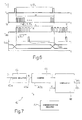
- the phase generator circuit 43 comprises an edge detector 45, a counter 46, a synchronization register 47, and a comparator 48.
- the edge detector 45 is connected to the first input 43a of the phase generator circuit 43 (fed with the first timing signal T 1 ) and supplies reset pulses R at rising edges of the first timing signal T 1 .
- the counter 46 has a reset input 46a receiving the reset pulses R, is connected to the second input 43b of the phase generator circuit 43 (fed with the third timing signal T 3 ) and has an output supplying a counting signal C which is incremented at each cycle of the third timing signal T 3 and hence has the third frequency F 3 .
- the comparator 48 has a first input connected to the output of the counter 46, and a second input connected to an output of the synchronization register 47, which supplies the delay K.
- an output 43c of the comparator 48 switches, supplying a decimation pulse T DEC .
- the delay K may be programmed by writing the synchronization register 47.
- the present noise compensating device generates a sampled signal BS having a frequency correlated to the signals present in the control loop 25.
- an acceleration signal S ACC may be generated, which represents accelerations due to disturbance forces acting on the R/W device 1 and is synchronous with the control signal S CONTR , without the need of sampling frequency conversions.
- the samples of the acceleration signal S ACC may be generated immediately before being used by the compensation block 22.
- the phase of the compensation signal S COMP is not degraded. Rather, the use of the numeric filter 39 to perform an equalization, enables minimization of the phase delay, and thus ensures a high effectiveness of the open loop noise compensation.
- Synchronization is moreover performed using a hardware circuit instead of a firmware procedure.
- the design phase is thus simplified, and it is possible to reduce both the size of the nonvolatile memory storing the firmware and the required processing power.
- the numeric filter 39 eliminates any noise outside of the frequency band, and in particular high frequency noise. Furthermore, the fact that the sensor assembly 17 is implemented by a single integrated device means that the noise affecting the acceleration signal S ACC is very contained.
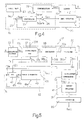
- a second embodiment hereinafter described with reference to Figure 8, regards a braking control system 50 for motor vehicles, in particular of the type commonly referred to as anti-lock braking system (ABS - from the German “AntiBlockierSystem”).
- ABS anti-lock braking system
- the braking control system 50 comprises a control unit 51, connected to a brake-operating device 52 for a wheel 53, an angular-velocity sensor 55, an acquisition stage 56, and a synchronization stage 57 identical to the synchronization stage 32 illustrated in Figures 5 and 7.
- the synchronization stage 57 comprises a phase-locked loop (PLL) 59 and a phase-generating circuit 60.
- the control unit 51 carries out separate and independent control of each wheel of the vehicle on which the braking control system 50 is mounted. For reasons of simplicity, in Figure 8 the components corresponding to the braking control of a single wheel 53 are illustrated.
- the control unit 51 which operates at an internal frequency, for example 5 MHz, has a first output 51a connected to an input of the brake-operating device 52 and supplying a brake control signal S BC , and a second output, connected to an input 59a of the PLL 59 and to an input 60a of the phase-generating circuit 60.
- the second output 51b of the control unit 51 supplies a timing control signal T CC which has a control frequency F CC equal to the frequency of the brake control signal S BC .
- the angular-velocity sensor 55 for example a dynamo driven by the wheel 53, has an output 55a supplying an analog angular-velocity signal V ⁇ , representative of the angular velocity of the wheel 53.
- the acquisition stage 56 is connected between the output 55a of the angular-velocity sensor 55 and an input 51c of the processing unit 51, and comprises a sigma-delta converter 61 and a decimator 62, cascade-connected.
- the acquisition stage 56 supplies, to the processing unit 51, a numeric angular-velocity signal S ⁇ , obtained from the analog angular-velocity signal V ⁇ .
- the control unit 51, the brake-operating device 52, the sensor 54, and the acquisition stage 56 form a control loop 63.
- the processing unit 51 detects locking of the wheel 53 and, in a per se known manner, acts on the brake-operating device 52 through the brake control signal S BC , so as to restore an optimal adherence of the wheel 53.
- the PLL 59 has an input 59a receiving the timing control signal T CC , a first output 59b, connected to a first input 61a of the A-D converter 61 and supplying a first oversampling signal T OS1 , and a second output 59c, connected to a timing input 62a of the decimator 62 and supplies a second oversampling signal T OS2 .
- the PLL 59 locks to the timing control signal T CC of the control loop 63 and generates the first oversampling signal T OS1 and the second oversampling signal T OS2 .
- These signals have, respectively, a first oversampling frequency F OS1 and a second oversampling frequency F OS2 , equal to respective integer multiples of the control frequency F CC of the timing control signal T CC and of the brake control signal S BC .
- first oversampling frequency F OS1 and the second oversampling frequency F OS2 may be equal to one another if the sigma-delta converter is able to output a new bit for each cycle of the first oversampling signal T OS1 ; otherwise, the first oversampling frequency F OS1 is higher than the second oversampling frequency F OS2 .
- the phase-generating circuit 60 has a first input 60a and a second input 60b which respectively receive the timing control signal T CC and the second oversampling signal T OS2 , and an output 60c, connected to a decimation input 62b of the decimator 62.
- the output 60c of the phase-generating circuit 60 supplies decimation pulses T DEC ' having a control frequency F CC and a delay K' which is preset and constant with respect to the timing control signal T CC .
- the delay K' indicates the signal to be selected by the decimator 62.
- the sigma-delta converter 61 receives, on a second input 59b, the analog angular-velocity signal V ⁇ and, using the first oversampling signal T OS1 as an internal timing signal, supplies, on an output 59c, a sampled signal BS' made up of a bit stream having the second oversampling frequency F OS2 .
- the brake control signal S BC works as a reference signal, and the control frequency F CC is used as a reference frequency.
- the PLL 59 locks to the timing control signal T CC , generated by the processing unit 51 synchronously with the brake control signal S BC . Thereby, the PLL 59 detects the control frequency F CC and generates the oversampling signals T OS1 , T OS2 with the respective oversampling frequencies F OS1 , F OS2 . These signals are then used to time the sigma-delta converter 61 and the decimator 62, as well as to generate the decimation pulses T DEC ' with a delay K' with respect to the timing control signal T CC .
- the phase generating circuit 60 comprises an edge detector 65, a counter 66, a synchronization register 67, and a comparator 68.
- the edge detector 65 is connected to the first input 60a of the phase generator 60 (receiving the timing control signal T CC ) and outputs reset pulses R' upon detection of rising edges of the first timing control signal T CC .
- the counter 66 has a reset input 66a receiving the reset pulses R', is connected to the second input 60b of the phase generator 60 (receiving the second oversampling signal T OS2 ), and has an output supplying a counting signal C' which is incremented at each cycle of the second oversampling signal T OS2 .
- the comparator 68 has a first input connected to the output of the counter 66 and a second input connected to an output of the synchronization register 67 which supplies the delay K'.
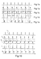
- the output of the comparator 68 switches, supplying a decimation pulse T DEC '. Consequently, at each cycle of the timing control signal T CC , exactly one decimation pulse T DEC ' is generated having a preset and constant delay K' from the respective edge of the timing control signal T CC , as illustrated in Figure 10.
- the delay K' is programmable by writing the synchronization register 67.
- the latency T L of the selected samples ( Figure 8), i.e., the time interval that elapses between a decimation pulse T DEC ' and the instant when the selected sample becomes usable by the processing unit 51, is reduced to a minimum. Consequently, also the phase margin of the braking-control system 50 is constant and may be optimized.
- the invention enables an advantageous utilization of sigma-delta converters also in closed-loop control systems, avoiding any degradation of the phase margin and any impairment of stability, since the invention carries out a high-precision, frequency and phase synchronization of two signals of numeric type, one of which is generated by a sigma-delta converter.
- the invention may be applied in all cases where it is necessary to generate a numeric signal that is synchronized both in frequency and in phase with a reference numeric signal.
Abstract
A device for generating synchronous numeric signals, including a
reference generating device supplying a reference signal and a first
timing signal (T1), both having a reference frequency
(F1); and a timed generating device (30,31,35) supplying a
synchronized signal (SACC) having the reference frequency
(F1). The device further includes a synchronization stage
generating a second timing signal (T2) having a first
controlled frequency (F2) correlated to the reference frequency
(F1), and phase synchronization pulses (TDEC) having
the first frequency (F1) and a preset delay (K) programmable
with respect to the first timing signal (T1).

Description
The present invention refers to a device and method for
generating synchronous numeric signals.
As is known, the use of numeric-type control systems is
increasingly widespread in various fields. As compared to
traditional purely analog control systems, in fact, numeric
control systems are extremely versatile and are, moreover,
very often simpler to design, less subject to failure, and
less costly. In practice, in numeric control systems a
microprocessor, or digital signal processor (DSP), receives,
through an analog-to-digital converter, a measured signal
correlated to a quantity to be controlled that is present in a
system controlled and sampled at a preset control frequency.
The measured signal is numerically processed to generate a
control signal (having a frequency equal to the control
frequency), which is supplied to an actuator for modifying the
state of the controlled system and for keeping the quantity to
be controlled close to a target value.
For numeric control systems to be efficient, it is, however,
necessary to provide accurate analog-to-digital converters
that convert with sufficient precision the signals supplied by
the sensors and/or transducers that are present. In
traditional A-D converters, the above aim is achieved by
generating a plurality of reference voltages, the values
whereof are normally determined by very precise resistive or
capacitive ratios. On the other hand, the fabrication of
resistive and capacitive components of controlled value
("matching") involves the use of sophisticated and costly
processing steps to minimize the inevitable process-induced
dispersions. In addition, all the resistive or capacitive
components used for generating the reference voltages should
respond in a homogeneous way to external stresses, for example
thermal stresses.
To overcome the problems outlined above, A-D converters of
sigma-delta type are in some cases preferred to traditional A-D
converters. In fact, sigma-delta A-D converters have a very
simple circuit structure and normally require a single
reference voltage to be generated: their fabrication thus
involves less complex and less costly processing steps and, in
addition, sigma-delta converters are less sensitive to
process-induced variations.
The use of these converters involves, however, a number of
problems. It is, in fact, known that a sigma-delta converter
receives an analog signal and outputs a sequence of bits that
represent the sign of the variations of the analog signal at
each operating cycle of the converter. To reconstruct a sample
representing the value of the analog signal at a given
instant, it is first of all necessary to oversample the analog
signal, feeding the sigma-delta converter with a timing signal
having a higher frequency than the control frequency. Then, by
through a decimator, it is necessary to filter the bit
sequence supplied by the sigma-delta converter and to select
filtered samples, eliminating excess samples, so as to obtain
a decimated signal having a decimation frequency equal to the
required control frequency.
Normally, however, the decimation frequency is only
approximately equal to the control frequency in that it is
impossible to guarantee that the frequency of the timing
signal will be exactly equal to an integer multiple of the
sampling frequency. Consequently, it may occur that, in
certain control cycles, no sample of the decimated signal will
be supplied to the microprocessor, or else that, instead, a
more recent sample will overwrite an older sample which has
not yet been used by the microprocessor.
For more clarity, a condition with the decimation frequency
lower than the control frequency is illustrated in Figures 1a-1e,
which show: the plot of a timing signal synchronous with
the control signal and activating control cycles (Figure 1a);
a sequence of decimation pulses (Figure 1b); switchings of the
decimated signal (Figure 1c); the latency of the samples of
the decimated signal, i.e., the time intervals between each
decimation and when the selected sample is made available to
the microprocessor (Figure 1d); and the instants at which a
new value of the control signal is supplied (Figure 1e).
As may be noted, in some control cycles no sample is taken
(i.e., no decimation pulses are present); consequently, in the
immediately following control cycles, the microprocessor is
not able to supply new values of the control signal, and wait
cycles with no control action occur.
On the other hand, it is known that the recurrent presence of
wait cycles, in which control actions cannot be performed,
significantly degrades the performance of the control system.
In addition, the phase delay of the decimated signal which is
read by the microprocessor and affects the stability of the
control system is variable and unpredictable, in so far as the
latency of the samples is variable.
Alternatively, it is possible to carry out a frequency
conversion before the data generated are read by the
microprocessor. In this case, the sequence of samples supplied
by the sigma-delta converter is initially filtered with a
reconstructing filter to generate a sequence of reconstructed
samples, and is then expanded, inserting between two
successive samples a first preset integer L of zero samples
corresponding to instants comprised in a same sampling
interval. The expanded sequence of data is then filtered
through a low-pass filter so as to replace the zero samples
with interpolated samples. Next, a decimation of the expanded
sequence of data is performed, keeping one sample every M
samples (M being a second pre-set integer) and eliminating all
the others. By choosing the numbers L and M in such a way that
the following condition is satisfied:
FC = L + 1 M FS
where FC is the control frequency and FS is the frequency of
the sequence of reconstructed samples, the decimated sequence
of data has a frequency equal to the control frequency FC and
may thus be used to generate the control signal.
However, also the frequency conversion causes an increase in
the phase margin, and hence adversely affects the stability of
the control system. Furthermore, frequency conversion is
performed using microprograms (firmware), and this entails
both problems of bulk in so far as it is necessary to provide
nonvolatile memories, and an increase in the required
processing power.
From the above, it is evident that the use of sigma-delta
converters that are not properly synchronized involves even
serious difficulties. In particular, the stability of the
control systems may be impaired.
The aim of the present invention is to overcome the drawbacks
of known devices and, in particular, to generate a numeric
signal synchronized in frequency and in phase with a reference
numeric signal.
According to the present invention there are provided a device
and a method for generating synchronous numeric signals, as
respectively claimed in Claim 1 and Claim 12.
For a better understanding of the present invention, a
preferred embodiment thereof is now described, purely as a
non-limiting example, with reference to the attached drawings,
wherein:
- Figures 1a-1e show plots versus time of quantities taken in a known control system ;
- Figure 2 is a simplified top plan view of a R/W system for a hard disk;
- Figure 3 is a side view of the device of Figure 2, in a section taken along plane III-III;
- Figure 4 is a simplified block diagram of a noise compensating device according to the present invention;
- Figure 5 is a more detailed block diagram of one part of the diagram of Figure 4, including a synchronization device according to a first embodiment of the present invention;
- Figure 6 shows the plot of quantities taken in the device of Figures 4 and 5;
- Figure 7 is a more detailed block diagram of one part of the diagram of Figure 5;
- Figure 8 shows a control system including a synchronization device according to a second embodiment of the present invention;
- Figure 9 is a more detailed block diagram of a part of the diagram of Figure 8; and
- Figure 10 shows the plot of quantities taken in the device according to Figures 8 and 9.
In the first described embodiment, the invention is applied to
a R/W device for hard disks.
With reference to Figures 2 and 3, an R/W device 1 for hard
disks is housed inside a casing 2 and comprises a plurality of
magnetic disks 7, a head-actuator assembly 4, and a control
card 5.
The magnetic disks 7 are mounted coaxially and rotationally
integral to a shaft 8 of a motor (not shown) and have each a
top surface 7a and a bottom surface 7b. In addition, control
information is stored, in a per se known manner, in preset
sectors of the magnetic disks 7.
The head-actuator assembly 4 comprises a rotating support 13
(generally referred to as E-block on account of its shape), a
plurality of suspension arms 11, integrally connected to the
rotating support 13, and a plurality of R/W heads 12 carried
by respective suspension arms 11; in use, each head 12 faces a
respective surface 7a, 7b of the magnetic disks 7, for reading
and writing. A motor 14 is connected to and drives the
rotating support 13 for positioning the R/W heads 12 on a
desired data track 15.
The control card 5 is carried by the casing 2 and comprises a
control unit 16 and a sensor assembly 17. In addition, the
control card 5 is connected to the motor 14 through a
connector of a known type (not shown).
As illustrated in Figure 4, the control unit 16 comprises a
logic unit 20, a controller 21, a compensation block 22, a
subtracting node 23, and an adding node 24.
The logic unit 20 generates, in a known way, a reference
signal SREF indicative of a target position for the read heads
12. The subtracting node 23 receives the reference signal SREF,
as well as a position signal SPOS fed on a first output of the
head-actuator assembly 4, in a known way. The output of the
subtracting node 23 is connected to an input of the controller
21. The controller 21 has an output connected to the adding
node 24 and supplying a control signal SCONTR. The head-actuator
assembly 4 has an input connected to the adding node 24 and a
second output connected to the sensor assembly 17 and
supplying a first timing signal T1. The control signal SCONTR
and the first timing signal T1 have a first frequency F1
determined by the rotation rate of the disks 7 and by the
number of control sectors. For instance, in a disk having an
angular speed of 5400 rpm and 60 control sectors, the first
frequency F1 is 5400 Hz.
The sensor assembly 17, which will be described in detail
later on with reference to Figure 5 and is preferably made as
a single integrated device, has an output connected to an
input of the compensation block 22. In addition, the sensor
assembly 17 supplies, on its output, an acceleration signal
SACC synchronized with the control signal SCONTR and
representative of an acceleration A due to noise forces, such
as mechanical vibrations, acting on the R/W device 1. The
compensation block 22 has an output connected to the adding
node 24 and supplying a compensation signal SCOMP.
In this way, the sensor assembly 17 and the compensation block
22 form an open loop compensation line 27. Furthermore, the
controller 21, the head-actuator assembly 4, the subtracting
node 23 and adding node 24 form a control loop 25.
The position signal SPOS supplied by the head-actuator assembly
4 is representative of the distance of the read heads 12 from
a center-of-track position and is generated when the read
heads 12 fly on the sectors of the magnetic disks 7 storing
the control information. In particular, the signal SPOS is
obtained, in a known way, by sampling an analog signal at the
first frequency F1. The error signal SERR and the control signal
SCONTR generated within the control loop 25 are synchronous with
the position signal SPOS, and hence have the first frequency F1.
The subtracting node 23 subtracts the position signal SPOS from
the reference signal SREF and generates an error signal SERR.
The error signal SERR is then used in the controller 21 to
obtain the control signal SCONTR, using any known control
technique (for example, a PID control technique).
The adding node 24 receives the control signal SCONTR and the
compensation signal SCOMP (synchronized to each other) and adds
them, to generate an actuation signal SATT supplied to the
head-actuator assembly 4 to correct the position of the read
heads 12.
With reference to Figure 5, the structure of the sensor
assembly 17 is now described, the output signal whereof
(acceleration signal SACC) is synchronized with the control
signal SCONTR.
The sensor assembly 17 comprises a sensing element 30, an
acquisition stage 31, a synchronization stage 32, and an
interface circuit 35.
The sensing element 30, preferably an acceleration sensor of
the rotational type, made using the MEMS (Micro-Electro-Mechanical
Systems) technology, detects the rotational
component of the acceleration A acting onto the R/W device 1,
for example on account of mechanical vibrations, and has an
output supplying a measure analog signal VM correlated to the
acceleration A.
The acquisition stage 31 is connected between the sensing
element 30 and the interface 35, and comprises an analog-to-digital
converter 37, preferably of the sigma-delta type, a
decimator 38, a numeric filter 39, a correction block 40, and
an output register 41, cascade-connected together. In
addition, the A/D converter 37 has a control output 37d
connected to a control input of the sensing element 30.
Thereby, the sensing element 30 and the A/D converter 37 form
an acquisition loop of the sigma-delta type, in itself known
and described, for example, in M. Lemkin and B. Boser, "A
Three Axis Micromachined Accelerometer with a CMOS Position-Sense
Interface and Digital Offset-Trim Electronics", IEEE
Journal of Solid State Circuits, Vol. 34, No. 4.
The synchronization stage 32 comprises a phase locked loop
(PLL) 42 and a phase generator circuit 43. The PLL 42 has an
input 42a receiving the first timing signal T1, a first output
42b connected to a first input 37a of the A/D converter 37 and
supplying a second timing signal T2, and a second output 42c
connected to the timing input 38a of the decimator 38 and to a
timing input 39b of the numeric filter 39 and supplying a
third timing signal T3. In the PLL 42, the second timing
signal T2 and the third timing signal T3 are generated as
described below, starting from the first timing signal T1.
The phase generator circuit 43 has inputs 43a and 43b
receiving the first timing signal T1 and, respectively, the
third timing signal T3, and an output 43c connected to a
decimation input 38b of the decimator 38 and to an activation
input 39c of the numeric filter 39. The output 43c of the
phase generator circuit 43 supplies decimation pulses TDEC at
the first frequency F1 and with a preset delay with respect to
the first timing signal T1.
The second timing signal T2 has a second frequency F2 not lower
than the first frequency F1, and the third timing signal T3 has
a third frequency F3 comprised between the second frequency F2
and the first frequency F1. In particular, the following
relationship apply: F2 = M*F1, and F3 = N*F1, where M and N are
two integers, with M ≥ N (for example, M = 224 and N = 32).
Consequently, since F2 = (M/N)*F3, the second frequency F2 is
greater than or equal to the third frequency F3. In addition,
the decimation pulses TDEC have the first frequency F1 of the
control signal SCONTR.
During operation of the R/W device 1, the PLL 42 locks to the
first timing signal T1 of the control loop 25 and generates
the second timing signal T2 and the third timing signal T3. In
turn, the phase generator circuit 43 generates decimation
pulses TDEC with a preset delay K with respect to the edges of
the first timing signal T1. The delay K is representative of
the sample to be selected by the decimator 38.
The A/D converter 37, preferably of the sigma-delta type,
receives, on a second input 37b, the analog measure signal VM
and, using the second timing signal T2 as internal timing
signal, issues, on an output 37c, a sampled signal BS formed
by a flow of bits oversampled with respect to the first
frequency F1. In particular, since the A/D converter 37 is of
the sigma-delta type, the individual bits of the sampled
signal BS are produced by the A/D converter 37 at the third
frequency F3.
In a per se known manner, the decimator 38 filters the sampled
signal BS received from the A/D converter 37 in order to
reconstruct an oversampled numeric signal, wherein every
sample includes a preset number of bits, and in order to
eliminate any high frequency components introduced by the
analog measure signal VM. Indeed, if these component are not
eliminated, decimation would cause a spectrum folding that, as
known, causes distortions. In addition, at each decimation
pulse TDEC, the decimator 38 selects and supplies a sample to a
data input 39a of the numeric filter 39, while the other
samples are eliminated. For example, at each cycle, the K-th
sample following the rising edge of the first timing signal T1
is selected, as illustrated in Figure 6, where the delay K is
an integer number comprised between 0 and N - 1. Since a
decimation pulse TDEC is generated at each cycle of the first
timing signal T1, the decimator 38 outputs samples that have
the same frequency F1 as the first timing signal T1 of the
control loop 25.
The numeric filter 39, which is preferably a second order
self-regression filter (or infinite impulse response IIR
filter) of a known type, filters the data received from the
decimator 38 to eliminate the high frequency noise components
and carry out a phase equalization in the frequency band of
interest (for example, from 0 Hz to 800 Hz). This enables the
phase delay introduced by the decimator 38 to be compensated
and reduced to the minimum.
The correction block 40 compensates the offsets and the gain
losses introduced by the acquisition stage 31 by adding an
offset term to the samples received and, respectively, by
multiplying the samples by a preset gain factor.
The signal at the output of the correction block 40 is the
acceleration signal S'ACC, which is stored in the FIFO type
output register 41 to be read preferably in an immediately
successive cycle of the first timing signal T1. In practice,
each sample of the acceleration signal SACC is representative
of the acceleration detected by the sensing element 30 during
the cycle that precedes the first timing signal T1 and is made
available through the interface 35 to be used by the
compensation block 22 from the start of a cycle that
immediately follows (as represented by the arrow in Figure 6).
In addition, thanks to the use of the timing signals T2, T3 and
the decimation pulses, respectively generated by the PLL 42
and by the phase generator circuit 43 starting from the first
timing signal T1, the acceleration signal SACC has the first
frequency F1 and is therefore synchronous with the signals
present in the control loop 25 (in particular, it is
synchronous with the control signal SCONTR).
As shown in Figure 7, the phase generator circuit 43 comprises
an edge detector 45, a counter 46, a synchronization register
47, and a comparator 48.
The edge detector 45 is connected to the first input 43a of
the phase generator circuit 43 (fed with the first timing
signal T1) and supplies reset pulses R at rising edges of the
first timing signal T1. The counter 46 has a reset input 46a
receiving the reset pulses R, is connected to the second input
43b of the phase generator circuit 43 (fed with the third
timing signal T3) and has an output supplying a counting
signal C which is incremented at each cycle of the third
timing signal T3 and hence has the third frequency F3.
The comparator 48 has a first input connected to the output of
the counter 46, and a second input connected to an output of
the synchronization register 47, which supplies the delay K.
When the counting signal C is equal to the delay K, an output
43c of the comparator 48 switches, supplying a decimation
pulse TDEC. Preferably, the delay K may be programmed by
writing the synchronization register 47.
Consequently, the present noise compensating device generates
a sampled signal BS having a frequency correlated to the
signals present in the control loop 25. Thereby, an
acceleration signal SACC may be generated, which represents
accelerations due to disturbance forces acting on the R/W
device 1 and is synchronous with the control signal SCONTR,
without the need of sampling frequency conversions. Moreover,
the samples of the acceleration signal SACC may be generated
immediately before being used by the compensation block 22. As
a consequence, the phase of the compensation signal SCOMP is not
degraded. Rather, the use of the numeric filter 39 to perform
an equalization, enables minimization of the phase delay, and
thus ensures a high effectiveness of the open loop noise
compensation.
Synchronization is moreover performed using a hardware circuit
instead of a firmware procedure. The design phase is thus
simplified, and it is possible to reduce both the size of the
nonvolatile memory storing the firmware and the required
processing power.
In addition, the numeric filter 39 eliminates any noise
outside of the frequency band, and in particular high
frequency noise. Furthermore, the fact that the sensor
assembly 17 is implemented by a single integrated device means
that the noise affecting the acceleration signal SACC is very
contained.
A second embodiment, hereinafter described with reference to
Figure 8, regards a braking control system 50 for motor
vehicles, in particular of the type commonly referred to as
anti-lock braking system (ABS - from the German
"AntiBlockierSystem").
The braking control system 50 comprises a control unit 51,
connected to a brake-operating device 52 for a wheel 53, an
angular-velocity sensor 55, an acquisition stage 56, and a
synchronization stage 57 identical to the synchronization
stage 32 illustrated in Figures 5 and 7. In particular, the
synchronization stage 57 comprises a phase-locked loop (PLL)
59 and a phase-generating circuit 60. Preferably, the control
unit 51 carries out separate and independent control of each
wheel of the vehicle on which the braking control system 50 is
mounted. For reasons of simplicity, in Figure 8 the components
corresponding to the braking control of a single wheel 53 are
illustrated.
The control unit 51, which operates at an internal frequency,
for example 5 MHz, has a first output 51a connected to an
input of the brake-operating device 52 and supplying a brake
control signal SBC, and a second output, connected to an input
59a of the PLL 59 and to an input 60a of the phase-generating
circuit 60. The second output 51b of the control unit 51
supplies a timing control signal TCC which has a control
frequency FCC equal to the frequency of the brake control
signal SBC.
The angular-velocity sensor 55, for example a dynamo driven by
the wheel 53, has an output 55a supplying an analog angular-velocity
signal VΩ, representative of the angular velocity of
the wheel 53.
The acquisition stage 56 is connected between the output 55a
of the angular-velocity sensor 55 and an input 51c of the
processing unit 51, and comprises a sigma-delta converter 61
and a decimator 62, cascade-connected. In particular, the
acquisition stage 56 supplies, to the processing unit 51, a
numeric angular-velocity signal SΩ, obtained from the analog
angular-velocity signal VΩ. In addition, the control unit 51,
the brake-operating device 52, the sensor 54, and the
acquisition stage 56 form a control loop 63.
If the numeric angular-velocity signal SΩ decreases rapidly
and approaches zero, the processing unit 51 detects locking of
the wheel 53 and, in a per se known manner, acts on the brake-operating
device 52 through the brake control signal SBC, so as
to restore an optimal adherence of the wheel 53.
The PLL 59 has an input 59a receiving the timing control
signal TCC, a first output 59b, connected to a first input 61a
of the A-D converter 61 and supplying a first oversampling
signal TOS1, and a second output 59c, connected to a timing
input 62a of the decimator 62 and supplies a second
oversampling signal TOS2.
During operation of the braking-control system 50, the PLL 59
locks to the timing control signal TCC of the control loop 63
and generates the first oversampling signal TOS1 and the second
oversampling signal TOS2. These signals have, respectively, a
first oversampling frequency FOS1 and a second oversampling
frequency FOS2, equal to respective integer multiples of the
control frequency FCC of the timing control signal TCC and of
the brake control signal SBC. In addition, the first
oversampling frequency FOS1 and the second oversampling
frequency FOS2 may be equal to one another if the sigma-delta
converter is able to output a new bit for each cycle of the
first oversampling signal TOS1; otherwise, the first
oversampling frequency FOS1 is higher than the second
oversampling frequency FOS2.
The phase-generating circuit 60 has a first input 60a and a
second input 60b which respectively receive the timing control
signal TCC and the second oversampling signal TOS2, and an
output 60c, connected to a decimation input 62b of the
decimator 62. The output 60c of the phase-generating circuit
60 supplies decimation pulses TDEC' having a control frequency
FCC and a delay K' which is preset and constant with respect to
the timing control signal TCC. The delay K' indicates the
signal to be selected by the decimator 62.
The sigma-delta converter 61 receives, on a second input 59b,
the analog angular-velocity signal VΩ and, using the first
oversampling signal TOS1 as an internal timing signal,
supplies, on an output 59c, a sampled signal BS' made up of a
bit stream having the second oversampling frequency FOS2.
In practice, the brake control signal SBC works as a reference
signal, and the control frequency FCC is used as a reference
frequency. The PLL 59, in fact, locks to the timing control
signal TCC, generated by the processing unit 51 synchronously
with the brake control signal SBC. Thereby, the PLL 59 detects
the control frequency FCC and generates the oversampling
signals TOS1, TOS2 with the respective oversampling frequencies
FOS1, FOS2. These signals are then used to time the sigma-delta
converter 61 and the decimator 62, as well as to generate the
decimation pulses TDEC' with a delay K' with respect to the
timing control signal TCC.
As shown in Figure 9, the phase generating circuit 60
comprises an edge detector 65, a counter 66, a synchronization
register 67, and a comparator 68.
The edge detector 65 is connected to the first input 60a of
the phase generator 60 (receiving the timing control signal
TCC) and outputs reset pulses R' upon detection of rising edges
of the first timing control signal TCC. The counter 66 has a
reset input 66a receiving the reset pulses R', is connected to
the second input 60b of the phase generator 60 (receiving the
second oversampling signal TOS2), and has an output supplying a
counting signal C' which is incremented at each cycle of the
second oversampling signal TOS2.
The comparator 68 has a first input connected to the output of
the counter 66 and a second input connected to an output of
the synchronization register 67 which supplies the delay K'.
When the counting signal C' is equal to the delay K', the
output of the comparator 68 switches, supplying a decimation
pulse TDEC'. Consequently, at each cycle of the timing control
signal TCC, exactly one decimation pulse TDEC' is generated
having a preset and constant delay K' from the respective edge
of the timing control signal TCC, as illustrated in Figure 10.
Preferably, the delay K' is programmable by writing the
synchronization register 67. Thereby, the latency TL of the
selected samples (Figure 8), i.e., the time interval that
elapses between a decimation pulse TDEC' and the instant when
the selected sample becomes usable by the processing unit 51,
is reduced to a minimum. Consequently, also the phase margin
of the braking-control system 50 is constant and may be
optimized.
From the above, it is clear that the invention enables an
advantageous utilization of sigma-delta converters also in
closed-loop control systems, avoiding any degradation of the
phase margin and any impairment of stability, since the
invention carries out a high-precision, frequency and phase
synchronization of two signals of numeric type, one of which
is generated by a sigma-delta converter.
More in general, the invention may be applied in all cases
where it is necessary to generate a numeric signal that is
synchronized both in frequency and in phase with a reference
numeric signal.
Claims (17)
- A device (4, 16, 17; 50) for generating synchronous numeric signals, comprising:characterized by synchronization means (32; 57) generating a second timing signal (T2; TOS1) having a first controlled frequency (F2; FOS1) correlated to said reference frequency (F1; FCC), and phase synchronization pulses (TDEC; TDEC') having said reference frequency (F1; FCC) and a preset delay (K; K') programmable with respect to said first timing signal (T1; TCC).reference generating means (4, 21; 51) supplying a reference signal (SCONTR; SBC) and a first timing signal (T1; TCC), both having a reference frequency (F1; FCC);timed generating means (30, 31, 35; 56) supplying a synchronized signal (SACC; SΩ) having said reference frequency (F1; FCC);
- A device according to Claim 1, characterized in that said timed generating means (30, 31, 35; 56) comprise:sampling means (37; 61) receiving an analog signal (VM; VΩ) and supplying a sampled signal (BS; BS') having a second controlled frequency (F3; FOS2) correlated to said reference frequency (F1; FCC) ; anda decimating stage (38-41, 35; 62) receiving said sampled signal (BS; BS') and said phase synchronization pulses (TDEC; TDEC') and generating said synchronized signal (SACC; SΩ) having said reference frequency (F1; FCC).
- A device according to Claim 2, characterized in that said synchronization means (32; 57) comprise:frequency generating means (42; 59) receiving said first timing signal (T1; TCC) and supplying said second timing signal (T2; TOS1) and a third timing signal (T3; TOS2) having said second controlled frequency (F3; FOS2) ; andphase generating means (43; 60) receiving said first timing signal (T1; TCC) and said third timing signal (T3; TOS2), and having an output (43c; 60c) connected to said decimating stage (38-41, 35, 22; 62) and supplying said synchronization pulses (TDEC; TDEC').
- A device according to Claim 3, characterized in that said first controlled frequency (F2; FOS1) and said second controlled frequency (F3; FOS2) are integer multiples (M, N) of said reference frequency (F1; FCC).
- A device according to Claim 3 or 4, characterized in that said sampling means (37; 61) have a timing input (37a; 61a), and in that said frequency generating means (42; 59) have a frequency sensing input (42a; 59a) receiving said first timing signal (T1; TCC), and a first output (42b; 59b) connected to said timing input (37a; 61a) and supplying said second timing signal (T2; TOS1).
- A device according to any of Claims 3-5, characterized in that said decimating stage (38-41, 35; 62) comprises a decimator circuit (38; 62) having a timing input (38a; 62a) connected to a second output (42c; 59c) of said frequency generating means (42; 59) and receiving said third timing signal (T3; TOS2), and a decimation input (38b; 62b) connected to said output (43c; 60c) of said phase generating means (43; 60) and receiving said synchronization pulses (TDEC; TDEC').
- A device according to any of Claims 3-6, characterized in that said frequency-generating means (42; 59) comprise a phase-locked loop (42; 59).
- A device according to any of Claims 3-7, characterized in that said phase-generating means (43; 60) comprise:counter means (46; 66) having a counting input (43b; 60b) receiving said third timing signal (T3; TOS2), a reset input (46a; 66a), and an output supplying a counting signal (C; C') which has said second controlled frequency (F3; FOS2) ; andreset means (45; 65) having an input (43a; 60a) and an output, said input of said reset means receiving said first timing signal (T1; TCC), and said output being connected to said reset input (46a; 66a) of said counter means (46; 66) and supplying reset pulses (R; R') at preset switching edges of said first timing signal (T1; TCC).
- A device according to Claim 8, characterized in that said phase generating means (43; 60) further comprise comparator means (48; 68) and memory means (47; 67); said memory means having an output supplying said delay (K; K'); and said comparator means (48; 68) having a first input connected to said output of said counter means (46; 66), a second input connected to said output of said memory means (47; 67), and an output (43c; 60c) supplying said synchronization pulses (TDEC; TDEC' ) when said counting signal (C; C') and said delay signal (K; K') are equal.
- A device according to Claim 9, characterized in that said delay (K; K') is programmable by writing said memory means (47; 67).
- A device according to any of the foregoing claims, characterized in that said sampling means (37; 61) comprise a sigma-delta converter.
- A method for generating synchronous numeric signals, comprising the step of:characterized by the step of:generating a reference signal (SCONTR; SBC) and a first timing signal (T1; TCC), both having a reference frequency (F1; FCC) ;generating, from said first timing signal (T1; TCC), a second timing signal (T2; TOS1) having a first controlled frequency (F2; FOS1) correlated to said reference frequency (F1; FCC), and phase synchronization pulses (TDEC; TDEC') having said reference frequency (F1; FCC) and a preset delay (K; K') programmable with respect to said first timing signal (T1; TCC).
- A method according to Claim 12, characterized by the steps of:sampling an analog signal (VM; VΩ), using said second timing signal (T2; TOS1), to generate a sampled signal (BS; BS') having a second controlled frequency (F3; FOS2) correlated to said reference frequency (F1; FCC) ;generating a third timing signal (T3; TOS2) having said second controlled frequency (F3; FOS2); anddecimating said sampled signal (BS; BS') using said third timing signal (T3; TOS2) and said phase synchronization pulses (TDEC; TDEC' ) to generate a synchronized signal (SACC; SΩ) having said reference frequency (F1; FCC).
- A method according to Claim 13, characterized in that said first controlled frequency (F2; FOS1) and said second controlled frequency (F3; FOS2) are integer multiples (M, N) of said reference frequency (F1; FCC).
- A method according to Claim 13 or 14, characterized in that said sampling step comprises performing an analog-to-digital conversion, and in that said decimation step comprises the step of selecting, for each cycle of said first timing signal (T1; TCC), a sample having said delay (K; K') with respect to preset switching edges of said first timing signal (T1; TCC).
- A method according to Claim 15, characterized in that said step of performing an analog-to-digital conversion is carried out by using a sigma-delta converter (37; 61) timed with said second timing signal (T2; TOS1).
- A method according to any of Claims 12-16, characterized by the step of programming said delay (K; K').
Priority Applications (3)
| Application Number | Priority Date | Filing Date | Title |
|---|---|---|---|
| EP00830775A EP1209809A1 (en) | 2000-11-24 | 2000-11-24 | Device and method for generating synchronous numeric signals |
| US10/032,862 US6661359B2 (en) | 2000-11-20 | 2001-10-25 | Device and method for generating synchronous numeric signals |
| JP2001359716A JP2002204158A (en) | 2000-11-24 | 2001-11-26 | Device and method for generating synchronous numeric signals |
Applications Claiming Priority (1)
| Application Number | Priority Date | Filing Date | Title |
|---|---|---|---|
| EP00830775A EP1209809A1 (en) | 2000-11-24 | 2000-11-24 | Device and method for generating synchronous numeric signals |
Publications (1)
| Publication Number | Publication Date |
|---|---|
| EP1209809A1 true EP1209809A1 (en) | 2002-05-29 |
Family
ID=8175565
Family Applications (1)
| Application Number | Title | Priority Date | Filing Date |
|---|---|---|---|
| EP00830775A Withdrawn EP1209809A1 (en) | 2000-11-20 | 2000-11-24 | Device and method for generating synchronous numeric signals |
Country Status (3)
| Country | Link |
|---|---|
| US (1) | US6661359B2 (en) |
| EP (1) | EP1209809A1 (en) |
| JP (1) | JP2002204158A (en) |
Cited By (1)
| Publication number | Priority date | Publication date | Assignee | Title |
|---|---|---|---|---|
| CN115996111A (en) * | 2023-03-24 | 2023-04-21 | 湖南迈克森伟电子科技有限公司 | Sampling clock signal generation method, symbol synchronization method and related device |
Families Citing this family (7)
| Publication number | Priority date | Publication date | Assignee | Title |
|---|---|---|---|---|
| DE10028033A1 (en) * | 2000-06-06 | 2001-12-13 | Kostal Leopold Gmbh & Co Kg | Providing digital current ripple signal from analog armature current signal of DC motor, involves including current ripple detected from oversampling in further evaluation when non-conformance is detected |
| ITTO20010693A1 (en) * | 2001-07-13 | 2003-01-13 | St Microelectronics Srl | DEVICE AND METHOD FOR THE GENERATION OF SYNCHRONOUS NUMERICAL SIGNALS WITH MINIMIZATION OF THE PHASE DELAY, IN CONTROL SYSTEMS WITH COM |
| JPWO2008152981A1 (en) * | 2007-06-12 | 2010-08-26 | 株式会社アルバック | Process management system |
| US8156264B2 (en) * | 2009-04-03 | 2012-04-10 | Analog Devices, Inc. | Digital output sensor FIFO buffer with single port memory |
| US8700205B2 (en) * | 2011-08-05 | 2014-04-15 | GM Global Technology Operations LLC | Moving stop station for robotic assembly |
| CN106571811B (en) * | 2015-10-09 | 2023-06-02 | 张伟林 | Synchronous compensation type three-phase motor synchronous control circuit |
| CN114252697B (en) * | 2020-09-23 | 2024-02-13 | 麦克维尔空调制冷(武汉)有限公司 | APF oversampling method, system and storage medium |
Citations (7)
| Publication number | Priority date | Publication date | Assignee | Title |
|---|---|---|---|---|
| US4746899A (en) * | 1986-10-07 | 1988-05-24 | Crystal Semiconductor Corporation | Method for reducing effects of electrical noise in an analog-to-digital converter |
| EP0384595A2 (en) * | 1989-02-22 | 1990-08-29 | Stc Plc | Digital phase shifter |
| EP0419823A1 (en) * | 1989-09-05 | 1991-04-03 | Motorola, Inc. | Digital time base generator with adjustable delay between two outputs |
| US5087829A (en) * | 1988-12-07 | 1992-02-11 | Hitachi, Ltd. | High speed clock distribution system |
| EP0602718A2 (en) * | 1992-12-16 | 1994-06-22 | Koninklijke Philips Electronics N.V. | Analog-to-digital converter for converting a multitude of analog input signals into digital output signals by means of one sigma-delta modulator |
| US5767720A (en) * | 1995-07-26 | 1998-06-16 | Kabushiki Kaisha Toshiba | Clock signal supplying circuit |
| US6057791A (en) * | 1998-02-18 | 2000-05-02 | Oasis Design, Inc. | Apparatus and method for clocking digital and analog circuits on a common substrate to enhance digital operation and reduce analog sampling error |
Family Cites Families (12)
| Publication number | Priority date | Publication date | Assignee | Title |
|---|---|---|---|---|
| US4472785A (en) | 1980-10-13 | 1984-09-18 | Victor Company Of Japan, Ltd. | Sampling frequency converter |
| US4902979A (en) * | 1989-03-10 | 1990-02-20 | General Electric Company | Homodyne down-converter with digital Hilbert transform filtering |
| US4965531A (en) * | 1989-11-22 | 1990-10-23 | Carleton University | Frequency synthesizers having dividing ratio controlled by sigma-delta modulator |
| US5619202A (en) * | 1994-11-22 | 1997-04-08 | Analog Devices, Inc. | Variable sample rate ADC |
| US5387913A (en) * | 1993-11-09 | 1995-02-07 | Motorola, Inc. | Receiver with digital tuning and method therefor |
| JP3674092B2 (en) * | 1995-08-09 | 2005-07-20 | ソニー株式会社 | Playback device |
| JP3321354B2 (en) | 1996-03-28 | 2002-09-03 | 株式会社日立製作所 | Positioning method, positioning device, and rotary storage device |
| US6172828B1 (en) * | 1996-05-16 | 2001-01-09 | Hitachi, Ltd. | Signal processing apparatus and a disk control apparatus, with head positioning control based on digitized servo data |
| JP3087833B2 (en) * | 1997-03-12 | 2000-09-11 | 日本電気株式会社 | Sample frequency converter |
| US6215423B1 (en) * | 1998-08-26 | 2001-04-10 | Motorola Inc. | Method and system for asynchronous sample rate conversion using a noise-shaped numerically control oscillator |
| US6341048B1 (en) | 1999-01-25 | 2002-01-22 | Seagate Technology Llc | Method and apparatus for servo data synchronization in a disc drive |
| US6580383B1 (en) * | 2000-11-01 | 2003-06-17 | Telasic Communications, Inc. | High resolution ADC based on an oversampled subranging ADC |
-
2000
- 2000-11-24 EP EP00830775A patent/EP1209809A1/en not_active Withdrawn
-
2001
- 2001-10-25 US US10/032,862 patent/US6661359B2/en not_active Expired - Lifetime
- 2001-11-26 JP JP2001359716A patent/JP2002204158A/en active Pending
Patent Citations (7)
| Publication number | Priority date | Publication date | Assignee | Title |
|---|---|---|---|---|
| US4746899A (en) * | 1986-10-07 | 1988-05-24 | Crystal Semiconductor Corporation | Method for reducing effects of electrical noise in an analog-to-digital converter |
| US5087829A (en) * | 1988-12-07 | 1992-02-11 | Hitachi, Ltd. | High speed clock distribution system |
| EP0384595A2 (en) * | 1989-02-22 | 1990-08-29 | Stc Plc | Digital phase shifter |
| EP0419823A1 (en) * | 1989-09-05 | 1991-04-03 | Motorola, Inc. | Digital time base generator with adjustable delay between two outputs |
| EP0602718A2 (en) * | 1992-12-16 | 1994-06-22 | Koninklijke Philips Electronics N.V. | Analog-to-digital converter for converting a multitude of analog input signals into digital output signals by means of one sigma-delta modulator |
| US5767720A (en) * | 1995-07-26 | 1998-06-16 | Kabushiki Kaisha Toshiba | Clock signal supplying circuit |
| US6057791A (en) * | 1998-02-18 | 2000-05-02 | Oasis Design, Inc. | Apparatus and method for clocking digital and analog circuits on a common substrate to enhance digital operation and reduce analog sampling error |
Cited By (2)
| Publication number | Priority date | Publication date | Assignee | Title |
|---|---|---|---|---|
| CN115996111A (en) * | 2023-03-24 | 2023-04-21 | 湖南迈克森伟电子科技有限公司 | Sampling clock signal generation method, symbol synchronization method and related device |
| CN115996111B (en) * | 2023-03-24 | 2023-06-27 | 湖南迈克森伟电子科技有限公司 | Sampling clock signal generation method, symbol synchronization method and related device |
Also Published As
| Publication number | Publication date |
|---|---|
| US20020087217A1 (en) | 2002-07-04 |
| US6661359B2 (en) | 2003-12-09 |
| JP2002204158A (en) | 2002-07-19 |
Similar Documents
| Publication | Publication Date | Title |
|---|---|---|
| CN107367271B (en) | Digital controller for micro-electromechanical gyroscope | |
| US7529320B2 (en) | Format efficient timing acquisition for magnetic recording read channels | |
| CN109073381B (en) | Secondary sensing loop with force feedback capability | |
| KR100570558B1 (en) | Synchronous digital demodulator with integrated read and servo channels | |
| EP1015849B1 (en) | A digital control system for a vibrating structure gyroscope | |
| US6591283B1 (en) | Efficient interpolator for high speed timing recovery | |
| US6487672B1 (en) | Digital timing recovery using baud rate sampling | |
| EP1209809A1 (en) | Device and method for generating synchronous numeric signals | |
| US6125154A (en) | Digital servo channel for recording apparatus | |
| US6985543B1 (en) | Digital servo channel for recording apparatus | |
| US5455813A (en) | Digital signal reproducing apparatus | |
| US6311140B1 (en) | Method and apparatus for servo data synchronization in a disc drive | |
| JP2004533740A (en) | Apparatus and method for adjusting a filter frequency in relation to a sampling frequency. | |
| US6492926B2 (en) | Noise compensation device and method in a discrete time control system | |
| US6078444A (en) | Read channel auxiliary high precision data conversion | |
| EP1115197B1 (en) | Digital FM stereo demodulator and method | |
| US20030039054A1 (en) | Device and method for generating synchronous numeric signals with phase-delay minimization in control systems with open-loop compensation | |
| EP1209677A1 (en) | Noise compensation device and method in a discrete time control system | |
| JP2006087059A (en) | Apparatus and method for generating equaly spaced pulse train | |
| JPH0681538B2 (en) | Rotating body control device | |
| JPH0475488A (en) | Digital servo apparatus |
Legal Events
| Date | Code | Title | Description |
|---|---|---|---|
| PUAI | Public reference made under article 153(3) epc to a published international application that has entered the european phase |
Free format text: ORIGINAL CODE: 0009012 |
|
| AK | Designated contracting states |
Kind code of ref document: A1 Designated state(s): AT BE CH CY DE DK ES FI FR GB GR IE IT LI LU MC NL PT SE TR |
|
| AX | Request for extension of the european patent |
Free format text: AL;LT;LV;MK;RO;SI |
|
| 17P | Request for examination filed |
Effective date: 20021128 |
|
| AKX | Designation fees paid |
Designated state(s): DE FR GB IT |
|
| 17Q | First examination report despatched |
Effective date: 20030129 |
|
| STAA | Information on the status of an ep patent application or granted ep patent |
Free format text: STATUS: THE APPLICATION IS DEEMED TO BE WITHDRAWN |
|
| 18D | Application deemed to be withdrawn |
Effective date: 20060601 |