EP1214780B1 - Emetteur de signaux radioelectriques modules a polarisation d'amplification auto-adaptee - Google Patents
Emetteur de signaux radioelectriques modules a polarisation d'amplification auto-adaptee Download PDFInfo
- Publication number
- EP1214780B1 EP1214780B1 EP00964349A EP00964349A EP1214780B1 EP 1214780 B1 EP1214780 B1 EP 1214780B1 EP 00964349 A EP00964349 A EP 00964349A EP 00964349 A EP00964349 A EP 00964349A EP 1214780 B1 EP1214780 B1 EP 1214780B1
- Authority
- EP
- European Patent Office
- Prior art keywords
- bias
- amplitude
- signals
- output
- voltage
- Prior art date
- Legal status (The legal status is an assumption and is not a legal conclusion. Google has not performed a legal analysis and makes no representation as to the accuracy of the status listed.)
- Expired - Lifetime
Links
Images

Classifications
-
- H—ELECTRICITY
- H04—ELECTRIC COMMUNICATION TECHNIQUE
- H04B—TRANSMISSION
- H04B1/00—Details of transmission systems, not covered by a single one of groups H04B3/00 - H04B13/00; Details of transmission systems not characterised by the medium used for transmission
- H04B1/02—Transmitters
- H04B1/04—Circuits
-
- H—ELECTRICITY
- H03—ELECTRONIC CIRCUITRY
- H03F—AMPLIFIERS
- H03F1/00—Details of amplifiers with only discharge tubes, only semiconductor devices or only unspecified devices as amplifying elements
- H03F1/02—Modifications of amplifiers to raise the efficiency, e.g. gliding Class A stages, use of an auxiliary oscillation
- H03F1/0205—Modifications of amplifiers to raise the efficiency, e.g. gliding Class A stages, use of an auxiliary oscillation in transistor amplifiers
- H03F1/0211—Modifications of amplifiers to raise the efficiency, e.g. gliding Class A stages, use of an auxiliary oscillation in transistor amplifiers with control of the supply voltage or current
- H03F1/0216—Continuous control
- H03F1/0222—Continuous control by using a signal derived from the input signal
- H03F1/0227—Continuous control by using a signal derived from the input signal using supply converters
-
- H—ELECTRICITY
- H03—ELECTRONIC CIRCUITRY
- H03F—AMPLIFIERS
- H03F1/00—Details of amplifiers with only discharge tubes, only semiconductor devices or only unspecified devices as amplifying elements
- H03F1/02—Modifications of amplifiers to raise the efficiency, e.g. gliding Class A stages, use of an auxiliary oscillation
- H03F1/0205—Modifications of amplifiers to raise the efficiency, e.g. gliding Class A stages, use of an auxiliary oscillation in transistor amplifiers
- H03F1/0261—Modifications of amplifiers to raise the efficiency, e.g. gliding Class A stages, use of an auxiliary oscillation in transistor amplifiers with control of the polarisation voltage or current, e.g. gliding Class A
-
- H—ELECTRICITY
- H03—ELECTRONIC CIRCUITRY
- H03F—AMPLIFIERS
- H03F3/00—Amplifiers with only discharge tubes or only semiconductor devices as amplifying elements
- H03F3/20—Power amplifiers, e.g. Class B amplifiers, Class C amplifiers
- H03F3/24—Power amplifiers, e.g. Class B amplifiers, Class C amplifiers of transmitter output stages
-
- H—ELECTRICITY
- H04—ELECTRIC COMMUNICATION TECHNIQUE
- H04B—TRANSMISSION
- H04B1/00—Details of transmission systems, not covered by a single one of groups H04B3/00 - H04B13/00; Details of transmission systems not characterised by the medium used for transmission
- H04B1/02—Transmitters
- H04B1/04—Circuits
- H04B2001/0408—Circuits with power amplifiers
Definitions
- Modulated radio signal transmitters are known for a long time and can be extremely varied. Modulation can be a phase and / or amplitude and / or frequency modulation. In the case amplitude modulation, and also in the case of certain modulation of phase, the modulated signals received at the input and those delivered at the output of the means power amplifiers have a continuously varying amplitude discreetly, that is, being able to take one of the values of a plurality predetermined discrete of distinct amplitude levels.
- EER envelope elimination / restoration in which we detect the envelope of the modulated signals from the modulator, the envelope of the signals modulated using an amplitude limiter, the transistor is saturated output power with high input power, we use for the polarization a PWM (pulse width modulation) switching converter with high frequency (the switching frequency must be much higher than that of the envelope of the modulated signals) which are piloted according to the envelope beforehand detected, so that the variation of the polarization provided by this converter allows to restore the envelope on the modulated signals at the output of the transistor output power.
- PWM pulse width modulation
- This technique is however limited by the values of switching frequency and is therefore not easily applicable to very high envelope frequencies, particularly in the field of transmission of high speed digital data (typically several megabits per second or tens of megabits per second between space systems - notably the satellites- and Earth).
- the realization of the envelope detector, the limiter, and of the converter is relatively complex - notably in the high speed transmission domain where the modulated signals have a carrier hyperfréquence-.
- the document "MICROWAVE POWER AMPLIFIER EFFICIENCY IMPROVEMENT WITH A 10MHz HBT DC-DC CONVERTER” Gary Hanington et al, International Microwave Symposium, Baltimore, 1998 IEEE MTT-S Digest WE2C-6 p. 589-592 teaches to detect the power of the modulated input signal of the amplifier with an RF coupler and an envelope detector, and to control the value of the bias voltage of the power amplification stage supplied by a PWM switching converter. Again, this solution is limited in frequency (the modulated signals can have a variation spectrum not exceeding 2 MHz for a chopping frequency between 10 and 20 MHz). In addition, its realization is relatively complex, especially when the modulated signals have a microwave carrier.
- the invention therefore aims to overcome all of these disadvantages and to propose a transmitter as mentioned and in which at minus the output power transistor (s) -especially all the transistors of power- present (s) a yield which remains optimized, i.e. is in always the best possible, even for low amplitude levels input signals, and which moreover is simple and inexpensive to produce and easily applicable in all signal carrier frequency ranges -including in the microwave field- and in all areas of signal variation frequency -including for high transmissions debit-.
- the invention thus aims to allow the implementation of a modulation such as an amplitude modulation of the M-QAM type in quadrature at M states, M being a power of 2, generating modulated signals at the input of amplification means whose amplitude varies according to a discrete plurality of amplitude levels, without significantly reducing the power consumption of the transmitter compared to other types of modulation in which the amplitude of the modulated input signals remains at least substantially constant, and this in a simple, economical and applicable to all areas of frequency, including microwave carriers and / or high transmissions debit.
- a modulation such as an amplitude modulation of the M-QAM type in quadrature at M states, M being a power of 2
- M being a power of 2
- the invention aims in particular to propose such a transmitter which does not require the use of a high PWM switching converter switching frequency, and which does not in fact impose any particular constraint on the frequency or technique of cutting, or even the use of such technique, to ensure the polarization of the power transistors.
- the invention also aims to propose such a transmitter in which the number of circuits crossed by the modulated signals, and which must transmit the carrier or be compatible with its frequency, is as low as possible.
- the invention aims to minimize the number of circuits transmitter microwave.
- the invention also aims to propose such a transmitter, the operation is reliable and precise, i.e. providing a modulated signal from Error-free amplitude level output.
- the invention also aims to propose such a transmitter which is in particularly suitable for space transmissions and which can be advantageously integrated aboard a spacecraft such as an artificial satellite - notably a terrestrial microsatellite - simple and economical.
- the transmitter according to the invention can be produced so extremely simple and economical, and in particular does not require any complex and efficient converter for the polarization of the transistors of power.
- the transmitter according to the invention also requires no circuit additional crossed by the carrier, or compatible with the frequency of the carrier - notably no microwave circuit when the carrier signal is in the microwave domain.
- the transmitter according to the invention does not in fact comprises only means for analyzing the control signals digital, and switching means, controlled at the rate of variations amplitude of the modulated output signals.
- the detection carried out for adapt the bias voltage of each power transistor in real time output does not operate on analog signals or at the modulation known in the prior art, which required detection relatively complex envelope.
- this detection is carried out by the means of analysis from the instantaneous digital value of the signals of digital controls (baseband), by a determination - notably by a logic circuit- of the amplitude level that the modulated output signals must present to code this numerical value, according to the modulation performed by the transmitter, which we also know the characteristics and logic.
- the invention does not use this determination (unlike the EER technique and the document cited) to develop the selection signal, but uses specific means of analysis which determine and / or calculate in parallel logically to from digital control signals (baseband) level amplitude corresponding to these digital control signals.
- the polarization means, the analysis means, and the switching means realize means for real-time adaptation of the bias voltage delivered by the bias means for at least one terminal of each output power transistor of the amplification means power, according to the instantaneous value to be taken by the modulated signals Release. And this adaptation is made not from the envelope of modulated signals from a modulation circuit, but from the signals control digital signals (baseband) to be transmitted. We thus obtain a much more precise and reliable adaptation, without high frequency circuit additional, and with simple and reliable polarization means.
- the polarization of the amplification means being controlled at from digital signals, errors or noise due to modulation are not not affected by the operation of power transistors, which is more reliable and precise.
- the means polarization delivering a discrete plurality of voltage levels are simpler, more economical and more reliable than in the prior art where it was necessary to use a PWM converter whose switching frequency and properties were to be adapted to provide a voltage that can be continuously variable.
- the switching frequency, the characteristics and the performance of the biasing means which provide levels of always identical voltage are in no way affected by amplitude variations of the modulated signals.
- the invention involves a some redundancy in determining the amplitude of modulation levels, this redundancy does not make the transmitter more complex and, in fact, induced on the contrary, great simplification and increased performance, including in the microwave domain.
- the analysis means are made up of a suitable electronic logic circuit to determine, from the instantaneous digital value of the digital control signals, said instantaneous amplitude level and to develop the representative selection signal of this instantaneous amplitude level.
- the logic circuit is adapted, depending on the modulation used, to determine the amplitude level of the modulated signals output corresponding to each bit stream of control signals digital. It is therefore a simple and reliable combinational logic, whose results are independent of errors and noise in analog circuits or microwave circuits.
- the invention relates to a transmitter such as mentioned above including a modulation circuit adapted to convert digital control signals into modulated analog signals, at least in amplitude, according to a discrete plurality of distinct amplitude levels predetermined, characterized in that the analysis means are suitable for develop and deliver, from digital control signals, a signal selection whose instantaneous value is representative of the amplitude level snapshot of the signals delivered by the modulation circuit.
- the amplitude modulation can be advantageously carried out by a specific circuit distinct from the means power amplification and polarization means.
- the amplitude modulation can be carried out, partially or entirely, by power amplification transistors, thanks to variations in polarization voltages.
- the modulation may only perform phase modulation (known as "PSK").
- PSK phase modulation
- the influence of the amplification means in the amplitude modulation depends the assembly of the power transistors, the operating class, and the how their different terminals are polarized from the means of polarization.
- the switching means For example, to avoid any effect of variations in polarization of the power transistors on the amplitude of the modulated signals of output, is varied, using the switching means, simultaneously the bias voltages of two terminals of each transistor (for example the bias voltage of the drain and the gate bias voltage for a common source field effect transistor).
- This double variation can be obtained at least in part by an appropriate choice of the operating class of the transistor, for example in class B for a field effect transistor. AT the opposite if only one terminal sees its bias voltage which varies, the transistor power will most often (except in class B) cause modulation amplitude of the modulated output signals.
- the means of modulation are M-QAM amplitude modulation means in quadrature at M states, M being a power of 2. It should be noted that the number of levels amplitude is not equal to the number of modulation states addressed in the plane complex. For example, for 16-QAM modulation, the modulated signals have only three amplitude levels.
- said plurality of discrete levels of bias voltage includes an integer N> 1 of bias voltage levels equal to the number of amplitude levels of said discrete plurality of amplitude levels of the modulated output signals, each level of bias voltage being associated and adapted to one and only one amplitude level.
- the same level of bias voltage can be associated and adapted to several amplitude levels, for example if the levels amplitude can be grouped into several groups of neighboring levels.
- each level of bias voltage is adapted so that the efficiency of each transistor of polarized output power with this level of bias voltage be optimum for the amplitude level of the modulated SMS output signals it delivers. More particularly, advantageously and according to the invention, each bias voltage level is adapted so that each transistor of polarized output power with this level of bias voltage delivers a output power which is of the order of its saturation start power for the amplitude level of the modulated output signals which it delivers.
- each transistor of output power of the amplification means is a field effect transistor receiving modulated input signals on its grid and delivering the signals output modules on its drain, in that the biasing means are adapted to be able to deliver a discrete plurality of voltage levels VD of polarization of the drain, and in that the switching means are suitable for control the value of the voltage VD for biasing the drain of each transistor of output power according to the value of the selection signal.
- the means polarization are also adapted to be able to deliver a discrete plurality of LV bias voltage levels of the gate, and in that the means of switching are suitable for controlling the value of the LV bias voltage of the gate of each output power transistor according to the value of the signal selection.
- the gain of the amplitude transistor can be maintained at less substantially constant despite variations in the bias voltage of the drain.
- the bias voltage of the VG gate allows control the average intensity of the current in the drain.
- the same effect can be obtained at least in part automatically from signals input modulated, if the power transistor is placed in a class of operation which allows such self-adaptation of the gain, for example by class B.
- the invention makes it possible to obtain a variation of the bias voltage of the drain and the average intensity in the drain allowing obtain optimum performance for each amplitude level, including lowest levels.
- the switching means are suitable for controlling the voltage value of polarization of at least one terminal of predetermined nature (identical for all similarly mounted transistors) of each transistor according to the value of selection signal. For example, we control the drain bias voltage of all transistors mounted in common source.
- each transistor of power of each stage is controlled by the selection signal.
- the Transmitter performance depends mainly on that of the output stage.
- the switching means are adapted to drive only each power transistor of the output stage of the means of amplification.
- Such a transmitter can find many applications and be suitable for many frequency ranges. He can nevertheless advantageously be suitable for transmitting signals with a carrier in the microwave domain, capable of transmitting digital data with a speed between 1 Mbits / s and 100 Mbits / s.
- the invention also relates to a transmitter characterized in combination for all or part of the characteristics mentioned above or below.
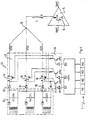
- the transmitter according to the invention schematically represented figure 1 receives digital data, say digital control signals 1, to be transmitted, which, in the example shown comprise four bits N1, N2, N3, N4.
- Digital control signals 1 are supplied to a converter digital / analog 2 which delivers two analog signals I, Q in quadrature, which, in turn, are supplied to a modulator circuit 3, the output of which supplies signals, called SME input modulated signals modulated on a delivered carrier by an oscillator 4 to the modulator circuit 3.
- the modulated SME input signals are supplied to a power amplifier 5 comprising at least one transistor of power 6, including at least one output power transistor which delivers modulated SMS output signals supplied to a transmitting antenna (not shown).
- Each power transistor 6 means amplifier 5 is polarized by polarization means 7 providing the bias voltages VD of drain and VG of gate of the power transistors 6 field effect.
- polarization means 7 comprise a source of direct voltage 8, which is for example the unregulated bar on board a satellite, or a storage battery or cells, means 9 converters to PWM cutting adapted to be able to deliver a discrete plurality predetermined separate bias voltage levels for the voltage of drain bias and / or for gate bias voltage, and means 10 switching devices adapted to apply at each instant to each of the terminals to bias a bias voltage from the converter means 9.
- a logic analysis circuit 11 collects the digital control signals 1, and is suitable for developing in real time, from the instantaneous value of digital control signals, a selection signal SS whose value instantaneous is representative of the instantaneous amplitude level to be taken by the modulated SMS output signals to be sent corresponding to this value instantaneous digital control signals 1.
- the modulator circuit 3 is a modulator, called 16 QAM, carrying out an amplitude modulation with 16 states.
- the signal amplitude can actually take three separate values A1, A2, A3. So; according to the value taken by the 4 bits N1, N2, N3, N4 of the digital control signals 1, and according to the value of the signals I and Q from converter 2, we can logically determine what the amplitude level A1, A2, A3 which must be taken by the modulated signals of SMS output.
- This combinatorial logic calculation is carried out by the logic circuit 11 which delivers a selection signal SS formed by 3 control bits B1, B2, B3 corresponding respectively to each of the amplitude levels A1, A2, A3. At each instant, only one of the control bits B1, B2, B3 is equal to 1, so that the selection signal SS is representative of the amplitude level A1, A2, A3 of the modulated SMS output signals.
- This SS selection signal is supplied to the switching means 10.
- Figure 4 shows in more detail the circuit for delivering the drain bias voltage VD to the amplification means 5.
- the means 9 converters are adapted to supply three bias voltages separate drain VD1, VD2, VD3, regulated by the converter means, and corresponding respectively to the amplitude levels A1, A2, A3 of the signals SMS output modules.
- the value of these bias voltages can be determined to adapt the operation of the power transistor 6 so that the latter has the best efficiency, depending on the input power Pe that it receives on its grid.
- the modulated input signals are amplitude modulated by the modulator circuit 3 and therefore have also three distinct amplitude levels corresponding to the three levels amplitude A1, A2, A3 of the modulated SMS output signals.
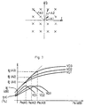
- Figure 3 shows the different curves representative of the output power Ps as a function of the input power Pe of a field effect output power transistor, according to the different bias voltages VD1, VD2, VD3. From a certain value of the input power, the power transistor exhibits a phenomenon of saturation. Also shown in Figure 3 are the curves illustrating the variations of the added efficiency ⁇ aj of the power transistor as a function of the power input Pe. As can be seen, when the drain bias voltage VD varies, the added efficiency ⁇ aj does not vary in maximum value, but shifts, the maximum of its yield being always located near the beginning of saturation of the transistor.
- Palim represents the power supply on the drain, i.e. is equal to the product of the drain bias voltage VD multiplied by the corresponding current ID.
- VD3 polarization of higher value
- the bias voltage VD2 is adapted so that the corresponding Ps (A2) output power is located at the start point of saturation, the efficiency added for this bias voltage VD being at its maximum.
- the voltage VD1 for which the power of Ps (A1) output of the lowest amplitude level is located at the limit value of saturation, the added yield still being at its maximum value.
- the switching means 10 comprise a switching circuit 12 receiving the different voltage values VD1, VD2, VD3 from converters 9, as well as the selection signal SS via a adaptation circuit 13 which enables three switching commands field effect transistors 14 used as circuit switches switching 12.
- These three transistors 14 are MOSFET transistors receiving at their source the voltage from converter 9 via a diode non-return 15.
- the adaptation circuit 13 receives the three digital signals B1, B2, B3 of the selection signal SS and includes, for each of them, a amplifier 16 supplying the base of a bipolar transistor 17 whose emitter is connected to ground and the collector is connected to the gate of the MOSFET transistor 14 corresponding, and, via a resistor 18, between the source of the MOSFET transistor 14 and diode 15. In this way, when bit B1 is equal to 1, the corresponding switching transistor 14 is in the on state and the circuit switching supplies the voltage VD1. Bits B2 and B3 being equal both at zero, the other two transistors 14 are in the off state.
- the three drains of transistors 14 being connected to a common node at output 19, this node 19 receives only one of the bias voltages VD1, VD2, VD3, and this as a function the value of bits B1, B2, B3 of the selection signal SS, itself determined to be representative of the amplitude level A1, A2, A3 of the modulated signals SMS output.
- the switching means 10 therefore select and apply at node 19 the optimum drain bias voltage level for the output power transistor 6. Under these conditions, it is understood that the added efficiency ⁇ aj of the power transistor 6 is always optimum.
- switching means 10 and the means 9 converters, as well as the logic analysis circuit 11 are extremely simple circuits which in no way convey the high frequency signals.
- the gate bias voltage VG can also be controlled, from similarly, so that the modulated SMS output signals do not have their amplitude modified according to the variations of the drain bias voltage VD. This result can also be obtained at least in part by choosing a appropriate operating class of output power transistor 6, for example class B.
- the circuit modulator 3 is not an amplitude modulator circuit, i.e. does not realize than PSK type phase modulation, so that the modulated signals EMS input always have at least substantially the same level amplitude.
- Amplitude modulation can then be carried out by means 5 amplification by choosing appropriate values from the different levels of bias voltage VD delivered to node 19 for power transistors 6. Indeed, the different levels of drain bias voltage vary like digital control signals 1 and like amplitude level correspondent for the modulated SMS output signals.
- the means modulation are therefore partly formed of the amplification means 5, and 11 analysis and 10 switching means.
- the invention is applicable to other types of modulation than 16-QAM modulation, and in particular with modulation having a greater number of states (32-QAM, 64-QAM ).
Description
- des moyens de modulation adaptés pour convertir les signaux de commande numériques en signaux modulés, dits signaux modulés d'entrée,
- des moyens d'amplification de puissance à état solide comportant au moins un transistor de puissance, dont au moins un transistor de puissance de sortie délivrant des signaux modulés de sortie,
- des moyens de polarisation comportant au moins une source de tension, et adaptés pour polariser chaque transistor de puissance des moyens d'amplification.
et en ce qu'il comprend :
- des moyens, dits moyens d'analyse, adaptés pour élaborer en temps réel à partir de la valeur instantanée des signaux de commande numériques, un signal, dit signal de sélection, dont la valeur instantanée est représentative du niveau d'amplitude instantané devant être pris par les signaux modulés de sortie à émettre correspondant à cette valeur instantanée des signaux de commande numériques, la valeur instantanée du signal de sélection variant avec les signaux de commande numériques selon une pluralité discrète de valeurs correspondant aux différents niveaux d'amplitude des signaux modulés de sortie,
- des moyens de commutation recevant le signal de sélection et adaptés pour sélectionner et appliquer à chaque instant, sur ladite borne à polariser, une tension de polarisation délivrée par les moyens de polarisation dont la valeur est égale au niveau de tension de polarisation associé et adapté au niveau d'amplitude représenté par la valeur instantanée du signal de sélection.
- la figure 1 est un schéma général d'un émetteur selon l'invention,
- la figure 2 est un diagramme illustrant un exemple de constellation dans le plan complexe correspondant à une modulation d'amplitude à 16 états,
- la figure 3 est un diagramme illustrant les variations des courbes de puissance de sortie et de rendement ajouté selon la tension de polarisation de drain VD d'un transistor de puissance à effet de champ monté en source commune,
- la figure 4 est un schéma d'un exemple de réalisation d'un émetteur selon l'invention.
Claims (10)
- Emetteur de signaux radioélectriques, dits signaux modulés de sortie (SMS), modulés au moins en amplitude selon une pluralité discrète de niveaux d'amplitude distincts prédéterminés (A1, A2, A3), à partir de signaux de commande numériques (1), comprenant :caractérisé en ce que les moyens (7) de polarisation sont adaptés pour pouvoir délivrer, pour au moins une borne à polariser de chaque transistor de puissance de sortie (6) des moyens (5) d'amplification, une pluralité discrète prédéterminée de niveaux de tension de polarisation distincts (VD1, VD2, VD3), chaque niveau de tension de polarisation étant associé et adapté à l'un au moins desdits niveaux d'amplitude (A1, A2, A3) des signaux modulés de sortie (SMS),des moyens (3) de modulation adaptés pour convertir les signaux de commande numériques (1) en signaux modulés, dits signaux modulés d'entrée (SME),des moyens (5) d'amplification de puissance à état solide comportant au moins un transistor de puissance, dont au moins un transistor de puissance de sortie (6) délivre des signaux modulés de sortie (SMS),des moyens (7) de polarisation comportant au moins une source de tension, et adaptés pour polariser chaque transistor de puissance des moyens (5) d'amplification,
et en ce qu'il comprend :des moyens, dits moyens (11) d'analyse, adaptés pour élaborer en temps réel à partir de la valeur instantanée des signaux de commande numériques (1), un signal, dit signal de sélection (SS), dont la valeur instantanée est représentative du niveau d'amplitude instantané devant être pris par les signaux modulés de sortie (SMS) à émettre correspondant à cette valeur instantanée des signaux de commande numériques (1), la valeur instantanée du signal de sélection (SS) variant avec les signaux de commande numériques (1) selon une pluralité discrète de valeurs correspondant aux différents niveaux d'amplitude (A1, A2, A3) des signaux modulés de sortie (SMS),des moyens (10) de commutation recevant le signal de sélection (SS) et adaptés pour sélectionner et appliquer à chaque instant, sur ladite borne à polariser, une tension de polarisation délivrée par les moyens (7) de polarisation dont la valeur est égale au niveau de tension de polarisation associé et adapté au niveau d'amplitude représenté par la valeur instantanée du signal de sélection (SS). - Emetteur selon la revendication 1, caractérisé en ce que les moyens (11) d'analyse sont formés d'un circuit électronique logique (11) adapté pour déterminer, à partir de la valeur numérique instantanée des signaux de commande numériques (1), ledit niveau d'amplitude instantané et pour élaborer le signal de sélection (SS) représentatif de ce niveau d'amplitude instantané.
- Emetteur selon l'une des revendications 1 et 2, comprenant un circuit de modulation (3) adapté pour convertir les signaux de commande numériques (1) en signaux analogiques modulés, au moins en amplitude, selon une pluralité discrète de niveaux d'amplitude distincts prédéterminés,
caractérisé en ce que les moyens (11) d'analyse sont adaptés pour élaborer et délivrer, à partir des signaux de commande numériques (1), un signal de sélection (SS) dont la valeur instantanée est représentative du niveau d'amplitude instantané des signaux délivrés par le circuit de modulation (3). - Emetteur selon l'une des revendications 1 à 3, caractérisé en ce que les moyens (3) de modulation sont des moyens de modulation d'amplitude M-QAM en quadrature à M états, M étant une puissance de 2.
- Emetteur selon l'une des revendications 1 à 4, caractérisé en ce que ladite pluralité discrète de niveaux de tension de polarisation comprend un nombre entier N>1 de niveaux de tension de polarisation (VD1, VD2, VD3) égal au nombre de niveaux d'amplitude (A1, A2, A3) de ladite pluralité discrète de niveaux d'amplitude des signaux modulés de sorte (SMS), chaque niveau de tension de polarisation étant associé et adapté à un et un seul niveau d'amplitude.
- Emetteur selon l'une des revendications 1 à 5, caractérisé en ce que chaque niveau de tension de polarisation est adapté pour que le rendement de chaque transistor de puissance de sortie (6) polarisé avec ce niveau de tension de polarisation soit optimum pour le niveau d'amplitude des signaux modulés de sortie (SMS) qu'il délivre.
- Emetteur selon l'une des revendications 1 à 6, caractérisé en ce que chaque niveau de tension de polarisation est adapté pour que chaque transistor de puissance de sortie (6) polarisé avec ce niveau de tension de polarisation délivre une puissance de sortie (Ps) qui est de l'ordre de sa puissance de début de saturation pour le niveau d'amplitude des signaux modulés de sortie (SMS) qu'il délivre.
- Emetteur selon l'une des revendications 1 à 7, caractérisé en ce que chaque transistor de puissance de sortie (6) des moyens (5) d'amplification est un transistor à effet de champ recevant des signaux modulés d'entrée (SME) sur sa grille et délivrant les signaux modulés de sortie (SMS) sur son drain, en ce que les moyens (7) de polarisation sont adaptés pour pouvoir délivrer une pluralité discrète de niveaux de tension VD de polarisation du drain, et en ce que les moyens (10) de commutation sont adaptés pour piloter la valeur de la tension VD de polarisation du drain de chaque transistor de puissance de sortie (6) selon la valeur du signal de sélection (SS).
- Emetteur selon l'une des revendications 1 à 8, caractérisé en ce que chaque transistor de puissance de sortie (6) des moyens (5) d'amplification est un transistor à effet de champ recevant des signaux modulés d'entrée (SME) sur sa grille et délivrant les signaux modulés de sortie (SMS) sur son drain, en ce que les moyens (7) de polarisation sont adaptés pour pouvoir délivrer une pluralité discrète de niveaux de tension VG de polarisation de la grille, et en ce que les moyens (10) de commutation sont adaptés pour piloter la valeur de la tension VG de polarisation de la grille de chaque transistor de puissance de sortie (6) selon la valeur du signal de sélection (SS).
- Emetteur selon l'une des revendications 1 à 9, caractérisé en ce qu'il est adapté pour l'émission de signaux avec une porteuse dans le domaine des hyperfréquences, et aptes à transmettre des données numériques avec un débit compris entre 1 Mbits/s et 100 Mbits/s.
Applications Claiming Priority (3)
| Application Number | Priority Date | Filing Date | Title |
|---|---|---|---|
| FR9911943A FR2799063B1 (fr) | 1999-09-24 | 1999-09-24 | Emetteur de signaux radioelectriques modules a polarisation d'amplification auto-adaptee |
| FR9911943 | 1999-09-24 | ||
| PCT/FR2000/002628 WO2001022572A1 (fr) | 1999-09-24 | 2000-09-22 | Emetteur de signaux radioelectriques modules a polarisation d'amplification auto-adaptee |
Publications (2)
| Publication Number | Publication Date |
|---|---|
| EP1214780A1 EP1214780A1 (fr) | 2002-06-19 |
| EP1214780B1 true EP1214780B1 (fr) | 2003-05-14 |
Family
ID=9550205
Family Applications (1)
| Application Number | Title | Priority Date | Filing Date |
|---|---|---|---|
| EP00964349A Expired - Lifetime EP1214780B1 (fr) | 1999-09-24 | 2000-09-22 | Emetteur de signaux radioelectriques modules a polarisation d'amplification auto-adaptee |
Country Status (7)
| Country | Link |
|---|---|
| US (1) | US7103114B1 (fr) |
| EP (1) | EP1214780B1 (fr) |
| JP (1) | JP2003510874A (fr) |
| AT (1) | ATE240607T1 (fr) |
| DE (1) | DE60002738T2 (fr) |
| FR (1) | FR2799063B1 (fr) |
| WO (1) | WO2001022572A1 (fr) |
Families Citing this family (46)
| Publication number | Priority date | Publication date | Assignee | Title |
|---|---|---|---|---|
| US6784748B1 (en) * | 2000-02-24 | 2004-08-31 | Skyworks Solutions, Inc. | Power amplifying system with supply and bias enhancements |
| EP1341300A1 (fr) * | 2002-02-27 | 2003-09-03 | Lucent Technologies Inc. | Amplificateur de puissance à courant de repos ajustable |
| AU2003272918A1 (en) * | 2002-10-03 | 2004-04-23 | Matsushita Electric Industrial Co., Ltd. | Transmitting method and transmitter apparatus |
| JP3985649B2 (ja) * | 2002-10-03 | 2007-10-03 | 松下電器産業株式会社 | 送信方法及び送信装置 |
| JP2005167805A (ja) * | 2003-12-04 | 2005-06-23 | Matsushita Electric Ind Co Ltd | 送信機 |
| JP2005252471A (ja) * | 2004-03-02 | 2005-09-15 | Fujitsu Ltd | 無線通信装置及びその増幅回路の制御方法 |
| DE102005034440A1 (de) | 2005-07-22 | 2007-02-01 | Infineon Technologies Ag | Verstärkeranordnung, Polartransmitter mit der Verstärkeranordnung und Verfahren zur Signalverstärkung |
| US8093946B2 (en) * | 2006-03-17 | 2012-01-10 | Nujira Limited | Joint optimisation of supply and bias modulation |
| GB2438457B (en) * | 2006-03-17 | 2011-09-14 | Nujira Ltd | Joint optimisation of supply and bias modulation |
| JP2009017388A (ja) * | 2007-07-06 | 2009-01-22 | Denso Corp | 差動増幅器および演算増幅器 |
| US8212541B2 (en) | 2008-05-08 | 2012-07-03 | Massachusetts Institute Of Technology | Power converter with capacitive energy transfer and fast dynamic response |
| JP5440498B2 (ja) * | 2008-06-13 | 2014-03-12 | 日本電気株式会社 | 電力増幅器及びその増幅方法、それを用いた電波送信機 |
| US8026763B2 (en) * | 2008-11-11 | 2011-09-27 | Massachusetts Institute Of Technology | Asymmetric multilevel outphasing architecture for RF amplifiers |
| JP5212316B2 (ja) * | 2009-09-03 | 2013-06-19 | 富士通株式会社 | 無線通信装置及び無線通信方法 |
| US8760148B1 (en) * | 2010-07-21 | 2014-06-24 | Anritsu Company | Pulse modulated PIM measurement instrument |
| JP5725026B2 (ja) * | 2010-08-03 | 2015-05-27 | 日本電気株式会社 | 電源変調器及びその制御方法 |
| EP2432118B1 (fr) | 2010-09-15 | 2012-12-26 | Agence Spatiale Européenne | Amplificateur d'alimentation de fréquence radio à suivi d'enveloppe rapide |
| JP2012129787A (ja) * | 2010-12-15 | 2012-07-05 | Hitachi Kokusai Electric Inc | 電源回路 |
| US10389235B2 (en) | 2011-05-05 | 2019-08-20 | Psemi Corporation | Power converter |
| US9882471B2 (en) | 2011-05-05 | 2018-01-30 | Peregrine Semiconductor Corporation | DC-DC converter with modular stages |
| CN103650313B (zh) | 2011-05-05 | 2018-09-21 | 北极砂技术有限公司 | 具有模块化的级的dc-dc转换器 |
| US10680515B2 (en) | 2011-05-05 | 2020-06-09 | Psemi Corporation | Power converters with modular stages |
| US9166536B2 (en) | 2012-10-30 | 2015-10-20 | Eta Devices, Inc. | Transmitter architecture and related methods |
| US8829993B2 (en) | 2012-10-30 | 2014-09-09 | Eta Devices, Inc. | Linearization circuits and methods for multilevel power amplifier systems |
| US9537456B2 (en) | 2012-10-30 | 2017-01-03 | Eta Devices, Inc. | Asymmetric multilevel backoff amplifier with radio-frequency splitter |
| US8824978B2 (en) | 2012-10-30 | 2014-09-02 | Eta Devices, Inc. | RF amplifier architecture and related techniques |
| US9210598B1 (en) | 2013-03-14 | 2015-12-08 | Anritsu Company | Systems and methods for measuring passive intermodulation (PIM) and return loss |
| US8619445B1 (en) | 2013-03-15 | 2013-12-31 | Arctic Sand Technologies, Inc. | Protection of switched capacitor power converter |
| US9331633B1 (en) | 2013-03-15 | 2016-05-03 | Anritsu Company | System and method for eliminating intermodulation |
| WO2014168911A1 (fr) | 2013-04-09 | 2014-10-16 | Massachusetts Institute Of Technology | Conversion de puissance à facteur de puissance élevé |
| US9654055B2 (en) | 2013-04-15 | 2017-05-16 | Agence Spatiale Europeenne | Radio-frequency high power amplifier with broadband envelope tracking by means of reversed buck converter |
| US9588212B1 (en) | 2013-09-10 | 2017-03-07 | Anritsu Company | Method of calibrating a measurement instrument for determining direction and distance to a source of passive intermodulation (PIM) |
| US10840805B2 (en) | 2013-09-24 | 2020-11-17 | Eta Devices, Inc. | Integrated power supply and modulator for radio frequency power amplifiers |
| US9755672B2 (en) | 2013-09-24 | 2017-09-05 | Eta Devices, Inc. | Integrated power supply and modulator for radio frequency power amplifiers |
| WO2015069516A1 (fr) | 2013-10-29 | 2015-05-14 | Massachusetts Institute Of Technology | Circuit de conversion d'énergie de transformateur à entraînement partagé à condensateur commuté |
| WO2016004427A1 (fr) | 2014-07-03 | 2016-01-07 | Massachusetts Institute Of Technology | Conversion de correction de facteur de puissance à haute fréquence et à haute densité pour interface de grille d'entrée universelle |
| US9768731B2 (en) | 2014-07-23 | 2017-09-19 | Eta Devices, Inc. | Linearity and noise improvement for multilevel power amplifier systems using multi-pulse drain transitions |
| US9455792B1 (en) | 2015-01-21 | 2016-09-27 | Anritsu Company | System and method for measuring passive intermodulation (PIM) in a device under test (DUT) |
| US9979421B2 (en) | 2015-03-02 | 2018-05-22 | Eta Devices, Inc. | Digital pre-distortion (DPD) training and calibration system and related techniques |
| US9768892B1 (en) | 2015-03-30 | 2017-09-19 | Anritsu Company | Pulse modulated passive intermodulation (PIM) measuring instrument with reduced noise floor |
| US9977068B1 (en) | 2015-07-22 | 2018-05-22 | Anritsu Company | Frequency multiplexer for use with instruments for measuring passive intermodulation (PIM) |
| US10541733B1 (en) * | 2017-11-05 | 2020-01-21 | Quantenna Communications, Inc. | Regulated switch banks for driving transmit power amplifiers of a MIMO wireless transceiver |
| KR20240012615A (ko) | 2019-07-08 | 2024-01-29 | 에타 와이어리스, 아이엔씨. | 차동 용량성 에너지 전달을 이용한 rf 전력 증폭기용의 다중 출력 공급 제너레이터 |
| US11637531B1 (en) | 2019-09-05 | 2023-04-25 | Murata Manufacturing Co., Ltd. | Supply generator and associated control methods |
| US11909358B1 (en) | 2020-01-22 | 2024-02-20 | Murata Manufacturing Co., Ltd. | Multilevel amplifier systems and related techniques |
| FR3118386B1 (fr) | 2020-12-22 | 2023-04-28 | Thales Sa | Systeme d'adaptation de la tension d'un drain d'un etage de puissance |
Family Cites Families (12)
| Publication number | Priority date | Publication date | Assignee | Title |
|---|---|---|---|---|
| US5123031A (en) * | 1989-02-08 | 1992-06-16 | Nokia-Mobira Oy | Control voltage generator in a transmitter arrangement for digitally modulated signals |
| JPH0511531U (ja) * | 1991-07-18 | 1993-02-12 | 三菱電機株式会社 | 電力合成fet増幅器 |
| US5608762A (en) * | 1993-06-30 | 1997-03-04 | Spectralink Corporation | Apparatus and method for automatic discriminator compensation in a FSK receiver |
| US5432473A (en) * | 1993-07-14 | 1995-07-11 | Nokia Mobile Phones, Limited | Dual mode amplifier with bias control |
| FR2716313B1 (fr) * | 1994-02-11 | 1996-04-12 | Alcatel Mobile Comm France | Dispositif de commande de la polarisation d'un amplificateur. |
| GB2296145B (en) * | 1994-12-15 | 1999-09-22 | Nokia Mobile Phones Ltd | Radio transmitters and methods of operation |
| US5933767A (en) * | 1997-09-15 | 1999-08-03 | Motorola, Inc. | Apparatus and method for tuning the gain of a transmitter utilizing cartesian feedback |
| US6084468A (en) * | 1997-10-06 | 2000-07-04 | Motorola, Inc. | Method and apparatus for high efficiency wideband power amplification |
| JPH11261434A (ja) * | 1998-03-09 | 1999-09-24 | Alps Electric Co Ltd | 変復調装置 |
| US5990750A (en) * | 1998-03-16 | 1999-11-23 | Lockheed Martin Corporation | Amplifier and driver system with multichannel operation |
| JP2000332622A (ja) * | 1999-05-20 | 2000-11-30 | Fujitsu General Ltd | 無線送信機 |
| US6429746B1 (en) * | 1999-12-07 | 2002-08-06 | Nokia Networks Oy | System and method for auto-bias of an amplifier |
-
1999
- 1999-09-24 FR FR9911943A patent/FR2799063B1/fr not_active Expired - Fee Related
-
2000
- 2000-09-22 EP EP00964349A patent/EP1214780B1/fr not_active Expired - Lifetime
- 2000-09-22 WO PCT/FR2000/002628 patent/WO2001022572A1/fr active IP Right Grant
- 2000-09-22 AT AT00964349T patent/ATE240607T1/de not_active IP Right Cessation
- 2000-09-22 DE DE60002738T patent/DE60002738T2/de not_active Expired - Lifetime
- 2000-09-22 US US10/088,797 patent/US7103114B1/en not_active Expired - Fee Related
- 2000-09-22 JP JP2001525833A patent/JP2003510874A/ja active Pending
Also Published As
| Publication number | Publication date |
|---|---|
| FR2799063A1 (fr) | 2001-03-30 |
| JP2003510874A (ja) | 2003-03-18 |
| ATE240607T1 (de) | 2003-05-15 |
| FR2799063B1 (fr) | 2001-12-21 |
| DE60002738T2 (de) | 2004-04-01 |
| WO2001022572A1 (fr) | 2001-03-29 |
| US7103114B1 (en) | 2006-09-05 |
| EP1214780A1 (fr) | 2002-06-19 |
| DE60002738D1 (de) | 2003-06-18 |
Similar Documents
| Publication | Publication Date | Title |
|---|---|---|
| EP1214780B1 (fr) | Emetteur de signaux radioelectriques modules a polarisation d'amplification auto-adaptee | |
| FR2835120A1 (fr) | Procede et dispositif de preparation de signaux destines a etre compares pour etablir une pre-distorsion sur l'entree d'un amplificateur | |
| EP0667675A1 (fr) | Dispositif de commande de la polarisation d'un amplificateur | |
| EP1269707B1 (fr) | Dispositif de production d'un signal radiofrequence module en phase et en amplitude | |
| EP2339744A1 (fr) | Circuit mélangeur basse tension pour un dispositif de transmission de signaux UWB | |
| WO2002101916A2 (fr) | Procede de modulation de l'amplitude d'un signal radiofrequence, et dispositif pour sa mise en oeuvre | |
| FR2922388A1 (fr) | Quantificateur, convertisseur analogique-numerique comprenant un tel quantificateur, et recepteur ultra-large bande integrant un tel convertisseur | |
| WO2002007303A1 (fr) | Circulation de modulation numerique de phase et amplitude et procede | |
| EP3245734A2 (fr) | Système de suivi de la puissance crête pour une amplification de puissance rf et procédé de calcul de valeur de crête et de sélection de tension d'alimentation associé | |
| EP2962390A1 (fr) | Système d'amplification de signaux | |
| EP3381123B1 (fr) | Bloc convertisseur continu-continu a multiples tensions d'alimentation, convertisseur continu-continu a multiples tensions d'alimentation le comprenant et systeme de suivi d'enveloppe associe | |
| EP0487386A1 (fr) | Dispositif doubleur de fréquence | |
| FR3005815B1 (fr) | Systeme de generation d'un signal analogique | |
| WO2020016305A1 (fr) | Architecture emettrice radiofrequence rf | |
| EP3482493A1 (fr) | Systeme de suivi de la puissance crete d'un signal de telecommunication et procede de calcul de valeur de crete et de selection de tension d'alimentation associe | |
| EP2182631A2 (fr) | Cellule amplificatrice hyperfréquences large bande à gain variable et amplificateur comportant une telle cellule | |
| EP3590190B1 (fr) | Cellule de commutation de puissance isolee | |
| FR2768277A1 (fr) | Emetteur ayant un rendement de puissance additionnelle ameliore et radio l'employant | |
| EP3984135B1 (fr) | Émetteur uwb compact à très basse consommation et forme d'onde reconfigurable | |
| EP1648084B1 (fr) | Mélangeur de signaux | |
| EP1089427A1 (fr) | Procédé de comparaison des amplitudes de deux signaux électriques | |
| CA2060413C (fr) | Procede de detection de signal perturbateur pour demodulateur de donnees numeriques et dispositif de mise en oeuvre d'un tel procede | |
| FR2683686A1 (fr) | Amplificateur de puissance micro-ondes. | |
| WO2000042710A1 (fr) | Emetteur de radiodiffusion en ondes courtes a haut rendement optimise pour les emissions de type numerique | |
| FR3068172A1 (fr) | Dispositif electronique a largeur de canal modulable |
Legal Events
| Date | Code | Title | Description |
|---|---|---|---|
| PUAI | Public reference made under article 153(3) epc to a published international application that has entered the european phase |
Free format text: ORIGINAL CODE: 0009012 |
|
| 17P | Request for examination filed |
Effective date: 20020314 |
|
| AK | Designated contracting states |
Kind code of ref document: A1 Designated state(s): AT BE CH CY DE DK ES FI FR GB GR IE IT LI LU MC NL PT SE |
|
| GRAH | Despatch of communication of intention to grant a patent |
Free format text: ORIGINAL CODE: EPIDOS IGRA |
|
| GRAH | Despatch of communication of intention to grant a patent |
Free format text: ORIGINAL CODE: EPIDOS IGRA |
|
| GRAA | (expected) grant |
Free format text: ORIGINAL CODE: 0009210 |
|
| AK | Designated contracting states |
Designated state(s): AT BE CH CY DE DK ES FI FR GB GR IE IT LI LU MC NL PT SE |
|
| PG25 | Lapsed in a contracting state [announced via postgrant information from national office to epo] |
Ref country code: NL Free format text: LAPSE BECAUSE OF FAILURE TO SUBMIT A TRANSLATION OF THE DESCRIPTION OR TO PAY THE FEE WITHIN THE PRESCRIBED TIME-LIMIT Effective date: 20030514 Ref country code: FI Free format text: LAPSE BECAUSE OF FAILURE TO SUBMIT A TRANSLATION OF THE DESCRIPTION OR TO PAY THE FEE WITHIN THE PRESCRIBED TIME-LIMIT Effective date: 20030514 Ref country code: IE Free format text: LAPSE BECAUSE OF FAILURE TO SUBMIT A TRANSLATION OF THE DESCRIPTION OR TO PAY THE FEE WITHIN THE PRESCRIBED TIME-LIMIT Effective date: 20030514 Ref country code: AT Free format text: LAPSE BECAUSE OF FAILURE TO SUBMIT A TRANSLATION OF THE DESCRIPTION OR TO PAY THE FEE WITHIN THE PRESCRIBED TIME-LIMIT Effective date: 20030514 |
|
| REG | Reference to a national code |
Ref country code: GB Ref legal event code: FG4D Free format text: NOT ENGLISH |
|
| REG | Reference to a national code |
Ref country code: CH Ref legal event code: EP |
|
| REG | Reference to a national code |
Ref country code: IE Ref legal event code: FG4D Free format text: FRENCH |
|
| REF | Corresponds to: |
Ref document number: 60002738 Country of ref document: DE Date of ref document: 20030618 Kind code of ref document: P |
|
| PG25 | Lapsed in a contracting state [announced via postgrant information from national office to epo] |
Ref country code: SE Free format text: LAPSE BECAUSE OF FAILURE TO SUBMIT A TRANSLATION OF THE DESCRIPTION OR TO PAY THE FEE WITHIN THE PRESCRIBED TIME-LIMIT Effective date: 20030814 Ref country code: DK Free format text: LAPSE BECAUSE OF FAILURE TO SUBMIT A TRANSLATION OF THE DESCRIPTION OR TO PAY THE FEE WITHIN THE PRESCRIBED TIME-LIMIT Effective date: 20030814 Ref country code: PT Free format text: LAPSE BECAUSE OF FAILURE TO SUBMIT A TRANSLATION OF THE DESCRIPTION OR TO PAY THE FEE WITHIN THE PRESCRIBED TIME-LIMIT Effective date: 20030814 Ref country code: GR Free format text: LAPSE BECAUSE OF FAILURE TO SUBMIT A TRANSLATION OF THE DESCRIPTION OR TO PAY THE FEE WITHIN THE PRESCRIBED TIME-LIMIT Effective date: 20030814 |
|
| PG25 | Lapsed in a contracting state [announced via postgrant information from national office to epo] |
Ref country code: ES Free format text: LAPSE BECAUSE OF FAILURE TO SUBMIT A TRANSLATION OF THE DESCRIPTION OR TO PAY THE FEE WITHIN THE PRESCRIBED TIME-LIMIT Effective date: 20030825 |
|
| PG25 | Lapsed in a contracting state [announced via postgrant information from national office to epo] |
Ref country code: LU Free format text: LAPSE BECAUSE OF NON-PAYMENT OF DUE FEES Effective date: 20030922 Ref country code: CY Free format text: LAPSE BECAUSE OF FAILURE TO SUBMIT A TRANSLATION OF THE DESCRIPTION OR TO PAY THE FEE WITHIN THE PRESCRIBED TIME-LIMIT Effective date: 20030922 |
|
| PG25 | Lapsed in a contracting state [announced via postgrant information from national office to epo] |
Ref country code: BE Free format text: LAPSE BECAUSE OF NON-PAYMENT OF DUE FEES Effective date: 20030930 Ref country code: MC Free format text: LAPSE BECAUSE OF NON-PAYMENT OF DUE FEES Effective date: 20030930 |
|
| GBT | Gb: translation of ep patent filed (gb section 77(6)(a)/1977) | ||
| NLV1 | Nl: lapsed or annulled due to failure to fulfill the requirements of art. 29p and 29m of the patents act | ||
| REG | Reference to a national code |
Ref country code: IE Ref legal event code: FD4D Ref document number: 1214780E Country of ref document: IE |
|
| PLBE | No opposition filed within time limit |
Free format text: ORIGINAL CODE: 0009261 |
|
| STAA | Information on the status of an ep patent application or granted ep patent |
Free format text: STATUS: NO OPPOSITION FILED WITHIN TIME LIMIT |
|
| BERE | Be: lapsed |
Owner name: CENTRE NATIONAL D'ETUDES SPATIALES *CNES ETABLISSE Effective date: 20030930 |
|
| 26N | No opposition filed |
Effective date: 20040217 |
|
| PG25 | Lapsed in a contracting state [announced via postgrant information from national office to epo] |
Ref country code: CH Free format text: LAPSE BECAUSE OF NON-PAYMENT OF DUE FEES Effective date: 20040930 Ref country code: LI Free format text: LAPSE BECAUSE OF NON-PAYMENT OF DUE FEES Effective date: 20040930 |
|
| REG | Reference to a national code |
Ref country code: CH Ref legal event code: PL |
|
| REG | Reference to a national code |
Ref country code: FR Ref legal event code: PLFP Year of fee payment: 17 |
|
| REG | Reference to a national code |
Ref country code: FR Ref legal event code: PLFP Year of fee payment: 18 |
|
| REG | Reference to a national code |
Ref country code: FR Ref legal event code: PLFP Year of fee payment: 19 |
|
| PGFP | Annual fee paid to national office [announced via postgrant information from national office to epo] |
Ref country code: DE Payment date: 20180913 Year of fee payment: 19 Ref country code: IT Payment date: 20180907 Year of fee payment: 19 Ref country code: FR Payment date: 20180928 Year of fee payment: 19 |
|
| PGFP | Annual fee paid to national office [announced via postgrant information from national office to epo] |
Ref country code: GB Payment date: 20180919 Year of fee payment: 19 |
|
| REG | Reference to a national code |
Ref country code: DE Ref legal event code: R119 Ref document number: 60002738 Country of ref document: DE |
|
| PG25 | Lapsed in a contracting state [announced via postgrant information from national office to epo] |
Ref country code: DE Free format text: LAPSE BECAUSE OF NON-PAYMENT OF DUE FEES Effective date: 20200401 |
|
| PG25 | Lapsed in a contracting state [announced via postgrant information from national office to epo] |
Ref country code: IT Free format text: LAPSE BECAUSE OF NON-PAYMENT OF DUE FEES Effective date: 20190922 |
|
| GBPC | Gb: european patent ceased through non-payment of renewal fee |
Effective date: 20190922 |
|
| PG25 | Lapsed in a contracting state [announced via postgrant information from national office to epo] |
Ref country code: FR Free format text: LAPSE BECAUSE OF NON-PAYMENT OF DUE FEES Effective date: 20190930 Ref country code: GB Free format text: LAPSE BECAUSE OF NON-PAYMENT OF DUE FEES Effective date: 20190922 |