EP1217700A2 - Large area laser - Google Patents
Large area laser Download PDFInfo
- Publication number
- EP1217700A2 EP1217700A2 EP01129143A EP01129143A EP1217700A2 EP 1217700 A2 EP1217700 A2 EP 1217700A2 EP 01129143 A EP01129143 A EP 01129143A EP 01129143 A EP01129143 A EP 01129143A EP 1217700 A2 EP1217700 A2 EP 1217700A2
- Authority
- EP
- European Patent Office
- Prior art keywords
- electrodes
- laser
- electrode
- gap
- discharge
- Prior art date
- Legal status (The legal status is an assumption and is not a legal conclusion. Google has not performed a legal analysis and makes no representation as to the accuracy of the status listed.)
- Granted
Links
- 239000004020 conductor Substances 0.000 claims description 16
- CURLTUGMZLYLDI-UHFFFAOYSA-N Carbon dioxide Chemical compound O=C=O CURLTUGMZLYLDI-UHFFFAOYSA-N 0.000 claims description 10
- 230000005284 excitation Effects 0.000 claims description 8
- 229910002092 carbon dioxide Inorganic materials 0.000 claims description 5
- 239000001569 carbon dioxide Substances 0.000 claims description 2
- 239000007789 gas Substances 0.000 description 14
- 238000000034 method Methods 0.000 description 9
- 230000003287 optical effect Effects 0.000 description 5
- 238000003491 array Methods 0.000 description 3
- 238000005259 measurement Methods 0.000 description 3
- IJGRMHOSHXDMSA-UHFFFAOYSA-N Atomic nitrogen Chemical compound N#N IJGRMHOSHXDMSA-UHFFFAOYSA-N 0.000 description 2
- 238000010276 construction Methods 0.000 description 2
- 238000001816 cooling Methods 0.000 description 2
- 238000009792 diffusion process Methods 0.000 description 2
- 239000012212 insulator Substances 0.000 description 2
- 238000007665 sagging Methods 0.000 description 2
- RYGMFSIKBFXOCR-UHFFFAOYSA-N Copper Chemical compound [Cu] RYGMFSIKBFXOCR-UHFFFAOYSA-N 0.000 description 1
- 230000015572 biosynthetic process Effects 0.000 description 1
- 230000015556 catabolic process Effects 0.000 description 1
- 239000000919 ceramic Substances 0.000 description 1
- 230000001427 coherent effect Effects 0.000 description 1
- 239000012809 cooling fluid Substances 0.000 description 1
- 229910052802 copper Inorganic materials 0.000 description 1
- 239000010949 copper Substances 0.000 description 1
- 238000006731 degradation reaction Methods 0.000 description 1
- 230000001419 dependent effect Effects 0.000 description 1
- 238000013461 design Methods 0.000 description 1
- 239000012153 distilled water Substances 0.000 description 1
- 230000000694 effects Effects 0.000 description 1
- 238000005516 engineering process Methods 0.000 description 1
- 229910052734 helium Inorganic materials 0.000 description 1
- 239000001307 helium Substances 0.000 description 1
- SWQJXJOGLNCZEY-UHFFFAOYSA-N helium atom Chemical compound [He] SWQJXJOGLNCZEY-UHFFFAOYSA-N 0.000 description 1
- 230000001976 improved effect Effects 0.000 description 1
- 230000001939 inductive effect Effects 0.000 description 1
- 230000001788 irregular Effects 0.000 description 1
- 239000007788 liquid Substances 0.000 description 1
- 239000000463 material Substances 0.000 description 1
- 230000007246 mechanism Effects 0.000 description 1
- 239000000203 mixture Substances 0.000 description 1
- 238000012986 modification Methods 0.000 description 1
- 230000004048 modification Effects 0.000 description 1
- 229910052757 nitrogen Inorganic materials 0.000 description 1
- 238000012545 processing Methods 0.000 description 1
- 230000001902 propagating effect Effects 0.000 description 1
- 239000007787 solid Substances 0.000 description 1
- 238000005728 strengthening Methods 0.000 description 1
- 230000008093 supporting effect Effects 0.000 description 1
- XLYOFNOQVPJJNP-UHFFFAOYSA-N water Chemical compound O XLYOFNOQVPJJNP-UHFFFAOYSA-N 0.000 description 1
Images


Classifications
-
- H—ELECTRICITY
- H01—ELECTRIC ELEMENTS
- H01S—DEVICES USING THE PROCESS OF LIGHT AMPLIFICATION BY STIMULATED EMISSION OF RADIATION [LASER] TO AMPLIFY OR GENERATE LIGHT; DEVICES USING STIMULATED EMISSION OF ELECTROMAGNETIC RADIATION IN WAVE RANGES OTHER THAN OPTICAL
- H01S3/00—Lasers, i.e. devices using stimulated emission of electromagnetic radiation in the infrared, visible or ultraviolet wave range
- H01S3/02—Constructional details
- H01S3/03—Constructional details of gas laser discharge tubes
- H01S3/0315—Waveguide lasers
-
- H—ELECTRICITY
- H01—ELECTRIC ELEMENTS
- H01S—DEVICES USING THE PROCESS OF LIGHT AMPLIFICATION BY STIMULATED EMISSION OF RADIATION [LASER] TO AMPLIFY OR GENERATE LIGHT; DEVICES USING STIMULATED EMISSION OF ELECTROMAGNETIC RADIATION IN WAVE RANGES OTHER THAN OPTICAL
- H01S3/00—Lasers, i.e. devices using stimulated emission of electromagnetic radiation in the infrared, visible or ultraviolet wave range
- H01S3/02—Constructional details
- H01S3/03—Constructional details of gas laser discharge tubes
- H01S3/038—Electrodes, e.g. special shape, configuration or composition
-
- H—ELECTRICITY
- H01—ELECTRIC ELEMENTS
- H01S—DEVICES USING THE PROCESS OF LIGHT AMPLIFICATION BY STIMULATED EMISSION OF RADIATION [LASER] TO AMPLIFY OR GENERATE LIGHT; DEVICES USING STIMULATED EMISSION OF ELECTROMAGNETIC RADIATION IN WAVE RANGES OTHER THAN OPTICAL
- H01S3/00—Lasers, i.e. devices using stimulated emission of electromagnetic radiation in the infrared, visible or ultraviolet wave range
- H01S3/09—Processes or apparatus for excitation, e.g. pumping
- H01S3/097—Processes or apparatus for excitation, e.g. pumping by gas discharge of a gas laser
- H01S3/0975—Processes or apparatus for excitation, e.g. pumping by gas discharge of a gas laser using inductive or capacitive excitation
-
- H—ELECTRICITY
- H01—ELECTRIC ELEMENTS
- H01S—DEVICES USING THE PROCESS OF LIGHT AMPLIFICATION BY STIMULATED EMISSION OF RADIATION [LASER] TO AMPLIFY OR GENERATE LIGHT; DEVICES USING STIMULATED EMISSION OF ELECTROMAGNETIC RADIATION IN WAVE RANGES OTHER THAN OPTICAL
- H01S3/00—Lasers, i.e. devices using stimulated emission of electromagnetic radiation in the infrared, visible or ultraviolet wave range
- H01S3/05—Construction or shape of optical resonators; Accommodation of active medium therein; Shape of active medium
- H01S3/08—Construction or shape of optical resonators or components thereof
- H01S3/081—Construction or shape of optical resonators or components thereof comprising three or more reflectors
- H01S3/0818—Unstable resonators
Definitions
- diffusion cooled gas discharge lasers Prior to the slab gas laser, diffusion cooled gas discharge lasers were characterized by output power per unit length of discharge and were typically limited to a maximum output power of 100 watts.
- the invention of the slab gas laser meant for the first time that the output power from diffusion cooled lasers could be scaled by discharge area rather than length only and could be characterized by a new figure of merit, watts output power per unit area of discharge. CO2 slab lasers of over three kilowatts are currently available commercially.
- the planar discharge of the slab CO2 laser is only typically one to two millimetres and the discharge electrodes are used as an optical waveguide.
- the slab laser is driven at high frequency, which is typically 100 MHz. With this discharge driving frequency the electrical wavelength is typically comparable to the dimensions of the laser structure. Standing waves of current and voltage occur across the discharge electrodes and the resulting discharge non-uniformity causes serious degradation of laser power unless corrective measures are taken.
- a method of reducing discharge non-uniformity resulting from electrical standing waves is a linear array of inductors connecting the discharge electrodes along the length of the discharge. This inductor array is placed on one or both sides of the electrode. This method is limited because it is linear and eliminates the standing wave only along the length of the electrodes. State of the art slab lasers are typically long and narrow so that this linear discharge method has been adequate. Attempts to scale slab lasers to very high power to meet the requirements of modern material processing machinery has resulted in the commercialization of slab lasers of large discharge area. Maximum output power of state of the art slab lasers is however limited by the area of discharge that is currently practicable. The length of the electrodes is limited by mechanical and thermal distortion of the waveguide to about 100 cm and the width is limited by standing wave induced discharge non- uniformity to about 20 cm.
- annular waveguide lasers have been disclosed as an alternative to planar slab lasers.
- a cylindrical structure is intrinsically more mechanically stable than a planar structure and a large area of discharge may be contained in a physically smaller structure than in a slab.
- the annular laser has not emerged as an alternative technology to the Slab laser because of practical difficulties.
- the formation of standing electrical standing wave along the length and around the circumference, the structural difficulties of driving and cooling coaxial cylindrical electrodes and the difficulties associated with obtaining a coherent laser beam from an annular waveguide has thus far prevented the practical use of annular waveguide gas lasers.
- This invention relates to an improved method of excitation of gas discharge lasers.
- a new method of electrical excitation of a slab discharge is disclosed.
- a two dimensional array of inductors is used to eliminate standing wave field patterns along the length and across the width of the electrodes. This method may be used to generate uniform gas discharge intensity for electrodes of arbitrary length, width and shape.
- the application of this new discharge balancing technique permits larger electrode area electrodes than is possible with prior art slab lasers and hence higher power.
- a laser comprising first and second electrodes disposed adjacent each other to form a gap between them, each of the first and second electrodes extending laterally; a laser gas disposed within the gap; means to provide electrical excitation to the first and second electrodes and generate a laser discharge within the gap; mirrors defining a resonator disposed at opposed ends of the gap; and an inductor array disposed across and along at least one of the first electrode and the second electrode to reduce lateral discharge non-uniformities.
- the inductor array is connected to the electrode and to a ground or reference plane.
- the laser is a gas slab laser with planar and preferably parallel electrodes.
- the resonator is preferably an unstable resonator.
- the inductor array is preferably connected to an external conductor acting as the ground or reference plane.
- the electrodes are cylindrical and have an annular discharge gap between them. In operation, the inductors cause a distributed parallel plate resonance between the electrodes, resulting in voltage variation across the width and length of the electrodes being less than 5%.
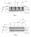
- the embodiments of the invention shown in Figs. 1, 2 and 3 each include a first electrode 10 and a second electrode 12 to which are connected in conventional fashion a high frequency excitation source 14 with a gap 11 between them.
- a common feature of these various embodiments is a two dimensional array 16A, 16B and 16C of inductors 18 connected to the high voltage electrode 10.
- the array extends across and along the electrode 10, with inductors 18 connected to the interior of the electrode 10 between lateral edges of the electrodes 10, 12.
- the inductors 18 connected to the high voltage electrode 10 are also connected to a ground or reference plane 20, which may be a continuous sheet or grid of conductors. In the embodiment shown in Fig. 1 the inductors 18 are connected by feedthroughs 21 to the ground plane electrode 12.
- the inductor array 16A extends across the electrode width as well as the electrode length.
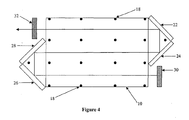
- Fig. 4 illustrates the distribution of the balancing inductors 18 with respect to the laser optics.
- connections 21 of the inductor array 16A to the ground electrode 12 presents an optical obstruction to the laser resonator. It is hence necessary in this embodiment to segment the resonator into parallel paths divided by the line of inductor connections. Possible resonators include an oscillator in one optical segment followed by amplifying stages in the remaining segments.
- FIG. 4 Another possible resonator, which is illustrated in Fig. 4, is a folded unstable resonator in which folding mirrors 22, 24, 26 and 28 are placed at opposite ends of the electrodes 10, 12.
- the folding mirrors 22, 24, 26 and 28 create multiple paths between the line of inductors 18 for the light to pass through the gap 11 between the electrodes 10, 12.
- the light reflects between the resonator mirrors 30 and 32 until the light discharges in conventional fashion at the output resonator mirror 32.
- FIG. 1 An advantage of the embodiment shown in Fig. 1 is that the inductor connections 21 to the grounded electrode 12 are insulated, typically with a ceramic insulator able to withstand the adjacent gas discharge. This insulator may also act as a support for the electrodes 10, 12 so that the problem of mechanical sagging that may occur in wide electrodes may be avoided.
- Fig. 2 shows an alternative embodiment of the invention where the discharge balancing inductors 18 are not connected to the ground electrode 12 but are connected to another ground plane 20 disposed on other the side of the ground electrode 12 from the high voltage electrode 10.
- This embodiment avoids the obstruction of the optical path by inductor connections such as feedthroughs 21.
- a disadvantage of this embodiment is that no supporting structures are positioned between the sides of the electrode so that in a wide structure where sagging may occur, strengthening structures will be required to maintain the electrode discharge gap uniformity across the electrode width.
- Figs. 1 and 2 are referred to in the high frequency electrical art as unbalanced structures.
- One electrode is held at high voltage and the other is held at a reference or ground voltage.
- Fig. 3 shows another embodiment of this invention, which is referred to in the electrical art as balanced.
- both electrodes 10, 12 are held at high voltage and both are connected to adjacent ground planes 20 by inductor arrays 16C.
- This embodiment shares the same advantages and disadvantages as the embodiment of Fig. 2.
- the disclosed inductor array does not share the limitations disclosed in prior art linear inductor arrays.
- the inductors 18 are of equal value and may be placed close to the electrode edges without causing non-uniformity of the discharge.
- the inductors are preferably disposed in an equidistant uniform pattern as illustrated in Fig. 4.
- the shape of the electrodes 10, 12 may be rectangular but they also may be irregular as may be required for folded optical resonators.
- the total inductance of the inductor arrays 16A, 16B, 16C and the total electrode capacitance preferably resonates close to the driving electrical frequency of the excitation source 14. This is not necessary for the generation of a uniform discharge but is desirable because the net reactance seen by the driving electrical circuit is minimized when the resonant condition is achieved.
- the inductor array disclosed in this invention behaves in a similar manner consistent with distributed parallel plate resonance.
- the electrodes are 35 cm long and 35 cm wide and are spaced to from a gap of 3 mm.
- the relative position of 16 inductors 18 connected across and along the high voltage electrode 10 is shown in Fig. 5 with inductors connected to the interior of the electrode, that is, the portion of the electrodes between the lateral edges.
- the rectangular spacing of the inductors 18 is 11.5 cm and inductors are placed about one centimeter from the electrode lateral edges 34.
- the electrode capacitance and the total inductance of the parallel inductors 18 resonate at a frequency of about 70 MHz, the driving frequency.
- the ground plane 20 which is disposed next to the high voltage electrode 10 is connected to the ground electrode 12 with a low impedance copper strip on the side of the electrodes 10, 12 opposite the driving point 36 (Fig. 2).
- the distribution of voltage across the high voltage electrode10 was measured using a high voltage high frequency voltmeter. The voltage was uniform at all point on the electrode 10 to within the 5% measurement error. This occurred despite the fact that as much as 10% variation in the inductance values of the inductors 18 was measured.
- an inductor array is applied to a large area annular discharge laser.
- the disclosed structure is physically less complex than prior art annular discharge lasers and the diameter of the discharge, and hence the laser power, may be scaled to high values.
- Prior art annular lasers are constructed using two coaxial cylindrical electrodes and the laser gas discharge is formed in an annular gap between the inner and outer cylindrical electrodes. Larger diameter annular prior art lasers require an outer electrode, which is split in order to achieve a uniform discharge around the circumference.
- Fig. 6 shows a schematic of an embodiment of this invention.
- This annular laser has a triaxial construction and is made up of an inner cylindrical electrode 40 and an outer cylindrical electrode 42 and the laser discharge is formed in an annular gap 44 between these electrodes in a similar manner to prior art annular laser.
- the outer discharge electrode is connected to the laser enclosure 45 and held at ground.
- a third cylindrical conductor 46 which surrounds the outer electrode 42, is used in the discharge excitation process.
- This cylindrical conductor is connected to the outer electrode 42 by an array of inductors 48 and is also connected to ground by a low impedance connection.
- the outer discharge electrode 42 is insulated from the laser structure and is connected to the high voltage driving electronics 50 by an insulated electrical feed-through 52. Cooling fluid, such as distilled water, is passed through both electrodes using insulating liquid flow tubes, which are not shown but are conventional for annular lasers.
- the three conductor coaxial assembly is mounted in a vacuum enclosure 45, which is used to enclose the electrodes 40, 42 in low pressure laser gases. This enclosure 45 may also be cylindrical but not necessarily.
- the inductors 48 are arrayed across (that is, around) the electrode 42 and along the length of the electrode 42 to form a two dimensional array with a typical spacing of 10 cm.
- Annular laser resonator mirrors 54 are mounted proximal and adjacent to both ends of the annular discharge 44 in conventional fashion.
- the mirrors 54 may be suspended from adjustment mechanisms mounted either on the ends of the laser enclosure 45 or on a thermo-mechanically stable resonator frame within the laser enclosure 45. This frame, the resonator mirrors 54 and the vacuum enclosure 45 are held at ground potential.
- Laser light outputs the laser enclosure 45 through an output window 56 in conventional fashion.
- a cylindrical electrode construction is electrically different from the large area planar slab laser. Electrical waves reflect from the edges of the electrodes 10, 12 of the slab laser and the reflected waves form complex standing waves, which are dependent upon the electrode shape. Unlike the slab laser, electrical waves will propagate unimpeded around the circumference of a cylindrical electrode and counter propagating waves form a standing wave and a non uniform discharge driving voltage. It is for this reason that prior art annular lasers with large diameter electrodes have split outer electrodes. In the disclosed annular laser, an array of inductors 48 disposed around the electrode perimeter and along the length of the electrodes is used to correct the standing waves. Notwithstanding that this annular structure is both mechanically and electrically very different from the large area planar slab laser an inductor array will reduce the electrical standing waves across the cylindrical electrode surfaces.
- an annular discharge structure had an inner cylindrical electrode diameter of 170 mm and an outer electrode diameter of 172 mm, which formed a discharge gap of 2 mm.
- the electrodes were precisely aligned to form a uniform discharge gap with variations of no more than +- 0.1 mm.
- Inductors of equal value were disposed across the electrode surface in a square array of inductors 89 mm apart, resonated at 72 MHz.
- the inductance value of the inductors was adjusted to enable an impedance match between the discharge and the high frequency power source used to drive the discharge.
- the electrical voltage distribution across the electrode surface, without the inductors in place varied by as much as 40% with a driving frequency of 100 MHz. With the inductor array in place the electrode voltage variation was reduced below the measurement accuracy of the instruments.
- the visible glow from the laser discharge which is an established indicator of discharge uniformity, was constant within measurement accuracy around the circumference.
- the inductors could be mounted inside an inner electrode 60 as shown in Fig. 7.
- An outer electrode 62 is concentrically mounted around the inner electrode 60 within vacuum enclosure 70 to form an annular discharge gap 64.
- the electrode 62 may be machined as part of the enclosure 70, and is grounded.
- the inner electrode 60 is supported within the enclosure 70 on electrical insulating mounts 78.
- Mirrors 66 disposed at either end of the discharge gap 64 form a resonator with an output window 67.
- Inductors 68 are distributed in an array across and along the inside of the inner electrode 60 and are connected to both the inner electrode 60 and a grounded conductor 72.
- the conductor 72 may also be formed as part of the vacuum enclosure 70.
- Inner electrode 60 is supplied with electrical energy from power supply 74 connected to the electrode 60 by electrical feed through 76.
- the inductors 68 cannot span the electrodes 60, 62 or they would block the beam.
- a central rod acting as a high voltage conductor 72 may be used if it were not too skinny and inductive. In this case the outer electrode 62 would be at ground, which is a desirable feature.
- the inner conductor 72 does not have to be a continuous plate.
- the laser is easier to build if the outer conductor, to which the inductors are connected, is a grid of conductors rather than a solid because it is then possible to measure the voltage across each inductor.
- the outer conductor for the annular laser and the large area slab with planar electrodes is a low impedance conductor connecting the electrodes through the inductor array.
- the preferred embodiment is one where the array of inductors does not span the gap and cause obstruction of the resonator.
- the outer conductor could be any shape that is convenient as for example, square.
- the electrodes 60, 62 may also have the form of segment of a cylinder, or follow any surface that is suitable for laser light propagation and that are large enough to form standing wave patterns, and are preferably parallel to each other.
- This annular discharge method is useful for any discharge structure where the size of the structure is comparable in size with the electrical wavelength of the discharge power supply so is not limited to waveguide structures.
- the laser gas may be that typically used in CO2 lasers, and may for example be a mixture of carbon dioxide, helium and nitrogen.
- the excitation frequency may be for example 10 MHz to 200 MHz and is chosen to generate a laser discharge within the laser gas.
- FIGs. 6 and 7 show sections in a plane that includes both the central axis and a diameter of the structure, it will be appreciated that a section perpendicular to the axis would show equally spaced inductors around one or both of the electrodes, as for example 89 mm apart in the example disclosed of the structure of Fig. 6.
Abstract
Description
Claims (14)
- A laser, comprising:first and second electrodes disposed adjacent each other to form a gap between them, each of the first and second electrodes extending laterally;a laser gas disposed within the gap;means to provide electrical excitation to the first and second electrodes and generate a laser discharge within the gap;mirrors defining a resonator disposed at opposed ends of the gap; andan inductor array disposed across and along at least one of the first electrode and the second electrode to reduce lateral discharge non-uniformities.
- The laser of claim 1 in which the first and second electrodes are planar.
- The laser of claim 1 or 2 in which the first and second electrodes are parallel to each other.
- The laser of any one of the preceding claims in which the inductor array is connected to an external conductor.
- The laser of claim 4 in which the external conductor is a continuous sheet.
- The laser of any one of the preceding claims in which, in operation, the inductors cause a distributed parallel plate resonance between the electrodes.
- The laser of claim 1 in which the electrodes are cylindrical and have an annular discharge gap between them.
- The laser of any one of the preceding claims in which the laser gas comprises carbon dioxide.
- The laser of any one of the preceding claims in which the resonator is an unstable resonator.
- The laser of any one of the preceding claims in which the inductor array is connected between the first electrode and the second electrode.
- The laser of claim 10 in which one of the first electrode and the second electrode is at a reference voltage.
- The laser of claim 11 in which the reference voltage is ground.
- A gas slab laser, comprising:electrodes disposed to form a gap between the electrodes, the electrodes having an interior extending between lateral edges of the electrodes, the electrodes forming a light guide for light travelling through the gap;an electrical power source applied to the electrodes for creating a gas discharge in the gap;a laser gas disposed in the gap;an unstable resonator disposed about the electrodes for guiding light within the gap in combination with the electrodes; andplural inductors connected to the interior of the electrodes to reduce lateral discharge nonuniformity and create a distributed parallel plate resonance between the electrodes.
- The gas slab laser of claim 13 further comprising inductors connected along the lateral edges of the electrodes.
Applications Claiming Priority (2)
| Application Number | Priority Date | Filing Date | Title |
|---|---|---|---|
| US25152000P | 2000-12-07 | 2000-12-07 | |
| US251520P | 2000-12-07 |
Publications (3)
| Publication Number | Publication Date |
|---|---|
| EP1217700A2 true EP1217700A2 (en) | 2002-06-26 |
| EP1217700A3 EP1217700A3 (en) | 2002-12-11 |
| EP1217700B1 EP1217700B1 (en) | 2004-10-13 |
Family
ID=22952314
Family Applications (1)
| Application Number | Title | Priority Date | Filing Date |
|---|---|---|---|
| EP01129143A Expired - Lifetime EP1217700B1 (en) | 2000-12-07 | 2001-12-06 | Large area laser |
Country Status (3)
| Country | Link |
|---|---|
| US (1) | US6704333B2 (en) |
| EP (1) | EP1217700B1 (en) |
| DE (1) | DE60106378T2 (en) |
Cited By (1)
| Publication number | Priority date | Publication date | Assignee | Title |
|---|---|---|---|---|
| WO2007144645A1 (en) * | 2006-06-14 | 2007-12-21 | Paul Mason | Light amplification device |
Families Citing this family (6)
| Publication number | Priority date | Publication date | Assignee | Title |
|---|---|---|---|---|
| US8599898B2 (en) * | 2004-12-22 | 2013-12-03 | Universal Laser Systems, Inc. | Slab laser with composite resonator and method of producing high-energy laser radiation |
| KR100708591B1 (en) | 2006-07-04 | 2007-04-18 | 한국과학기술원 | Method and apparatus for distributing clock signal having standing waveform |
| US7778303B2 (en) * | 2007-11-02 | 2010-08-17 | Trumpf, Inc. | Laser having distributed inductances |
| WO2012058685A2 (en) | 2010-10-29 | 2012-05-03 | Trumpf, Inc. | Rf-excited laser assembly |
| DE102012222469B4 (en) | 2012-12-06 | 2017-03-30 | Trumpf Laser- Und Systemtechnik Gmbh | A diffusion cooled gas laser array and method of adjusting the discharge distribution in a diffusion cooled gas laser array |
| TWI590753B (en) * | 2016-11-02 | 2017-07-01 | 和碩聯合科技股份有限公司 | Pin protective cover and bi-directional optical sub-assemblies device using the same |
Citations (6)
| Publication number | Priority date | Publication date | Assignee | Title |
|---|---|---|---|---|
| US4352188A (en) * | 1980-07-03 | 1982-09-28 | Hughes Aircraft Company | rf Pumped waveguide laser with inductive loading for enhancing discharge uniformity |
| US4443877A (en) * | 1982-02-01 | 1984-04-17 | United Technologies Corporation | Uniformly excited RF waveguide laser |
| US4601039A (en) * | 1983-09-01 | 1986-07-15 | The Regents Of The University Of California | Inductively stabilized, long pulse duration transverse discharge apparatus |
| JPS6469084A (en) * | 1987-09-10 | 1989-03-15 | Toshiba Corp | Gas laser equipment |
| US4939738A (en) * | 1987-08-31 | 1990-07-03 | Deutsche Forschung -Und Versuchsanstalt | High-power waveguide laser |
| WO1995005060A1 (en) * | 1993-08-05 | 1995-02-16 | Lumonics Limited | A radiofrequency gas discharge |
Family Cites Families (5)
| Publication number | Priority date | Publication date | Assignee | Title |
|---|---|---|---|---|
| US4363126A (en) * | 1980-12-10 | 1982-12-07 | United Technologies Corporation | Tuned-circuit RF-excited laser |
| US4719639B1 (en) | 1987-01-08 | 1994-06-28 | Boreal Laser Inc | Carbon dioxide slab laser |
| DE3828951A1 (en) | 1988-08-26 | 1990-03-01 | Deutsche Forsch Luft Raumfahrt | WAVE GUIDE ARRANGEMENT |
| US5079773A (en) * | 1991-01-15 | 1992-01-07 | United Technologies Corporation | Tailored cross section optical waveguide laser array |
| US5610936A (en) * | 1995-09-28 | 1997-03-11 | Technology Development Corporation | Extended multiply folded optical paths |
-
2001
- 2001-12-05 US US10/001,925 patent/US6704333B2/en not_active Expired - Fee Related
- 2001-12-06 EP EP01129143A patent/EP1217700B1/en not_active Expired - Lifetime
- 2001-12-06 DE DE60106378T patent/DE60106378T2/en not_active Expired - Lifetime
Patent Citations (6)
| Publication number | Priority date | Publication date | Assignee | Title |
|---|---|---|---|---|
| US4352188A (en) * | 1980-07-03 | 1982-09-28 | Hughes Aircraft Company | rf Pumped waveguide laser with inductive loading for enhancing discharge uniformity |
| US4443877A (en) * | 1982-02-01 | 1984-04-17 | United Technologies Corporation | Uniformly excited RF waveguide laser |
| US4601039A (en) * | 1983-09-01 | 1986-07-15 | The Regents Of The University Of California | Inductively stabilized, long pulse duration transverse discharge apparatus |
| US4939738A (en) * | 1987-08-31 | 1990-07-03 | Deutsche Forschung -Und Versuchsanstalt | High-power waveguide laser |
| JPS6469084A (en) * | 1987-09-10 | 1989-03-15 | Toshiba Corp | Gas laser equipment |
| WO1995005060A1 (en) * | 1993-08-05 | 1995-02-16 | Lumonics Limited | A radiofrequency gas discharge |
Non-Patent Citations (2)
| Title |
|---|
| BETHEL J W ET AL: "A new scalable annular CO2 laser with high specific output power" OPTICS COMMUNICATIONS, NORTH-HOLLAND PUBLISHING CO. AMSTERDAM, NL, vol. 145, no. 1-6, 1998, pages 352-358, XP004102723 ISSN: 0030-4018 * |
| PATENT ABSTRACTS OF JAPAN vol. 013, no. 285 (E-780), 29 June 1989 (1989-06-29) -& JP 01 069084 A (TOSHIBA CORP), 15 March 1989 (1989-03-15) * |
Cited By (2)
| Publication number | Priority date | Publication date | Assignee | Title |
|---|---|---|---|---|
| WO2007144645A1 (en) * | 2006-06-14 | 2007-12-21 | Paul Mason | Light amplification device |
| GB2441486A (en) * | 2006-06-14 | 2008-03-05 | Paul Mason | Light amplification device |
Also Published As
| Publication number | Publication date |
|---|---|
| DE60106378T2 (en) | 2006-03-09 |
| DE60106378D1 (en) | 2004-11-18 |
| US20040013150A1 (en) | 2004-01-22 |
| US6704333B2 (en) | 2004-03-09 |
| EP1217700B1 (en) | 2004-10-13 |
| EP1217700A3 (en) | 2002-12-11 |
Similar Documents
| Publication | Publication Date | Title |
|---|---|---|
| US5123028A (en) | RF Excited CO2 slab waveguide laser | |
| US5386431A (en) | Regenerative amplifier laser array | |
| US5140606A (en) | RF excited CO2 slab waveguide laser | |
| US5748663A (en) | Retangular discharge gas laser | |
| US4688228A (en) | Phase locked dielectric ridge gas laser | |
| US4481634A (en) | RF Excited metal waveguide laser | |
| US4513424A (en) | Laser pumped by X-band microwaves | |
| US4891819A (en) | RF excited laser with internally folded resonator | |
| EP1217700B1 (en) | Large area laser | |
| US5689523A (en) | Excitation system for multi-channel lasers | |
| JP6129410B2 (en) | Laser tube with baffle | |
| US6298806B1 (en) | Device for exciting a gas by a surface wave plasma | |
| US4807234A (en) | Phase locked alternating dielectric ridge gas laser | |
| US5283797A (en) | RF excited CO2 slab waveguide laser | |
| US4677637A (en) | TE laser amplifier | |
| WO2021158396A1 (en) | Radio-frequency excited gas laser | |
| US5648980A (en) | Excitation system for multi-channel lasers | |
| US5379317A (en) | Microwave-excited slab waveguide laser with all metal sealed cavity | |
| US5155739A (en) | RF excited CO2 slab waveguide laser | |
| EP0486152B1 (en) | Gas slab laser | |
| EP0776073B1 (en) | Gas laser having a rectangular discharge space | |
| US4387463A (en) | Electrical discharge apparatus and a gas laser pumped by an electrical discharge through the gas | |
| US5131004A (en) | RF excited CO2 slab waveguide laser | |
| JPS61259586A (en) | Wireless frequency transformer, diagnosis thereof and wireless frequency exciting gas laser | |
| Xin et al. | Radio-frequency excited one-dimensional limit parameter waveguide array CO 2 laser |
Legal Events
| Date | Code | Title | Description |
|---|---|---|---|
| PUAI | Public reference made under article 153(3) epc to a published international application that has entered the european phase |
Free format text: ORIGINAL CODE: 0009012 |
|
| AK | Designated contracting states |
Kind code of ref document: A2 Designated state(s): AT BE CH CY DE DK ES FI FR GB GR IE IT LI LU MC NL PT SE TR |
|
| AX | Request for extension of the european patent |
Free format text: AL;LT;LV;MK;RO;SI |
|
| PUAL | Search report despatched |
Free format text: ORIGINAL CODE: 0009013 |
|
| AK | Designated contracting states |
Kind code of ref document: A3 Designated state(s): AT BE CH CY DE DK ES FI FR GB GR IE IT LI LU MC NL PT SE TR |
|
| AX | Request for extension of the european patent |
Free format text: AL;LT;LV;MK;RO;SI |
|
| 17P | Request for examination filed |
Effective date: 20030606 |
|
| 17Q | First examination report despatched |
Effective date: 20030710 |
|
| AKX | Designation fees paid |
Designated state(s): DE FR GB IT |
|
| GRAP | Despatch of communication of intention to grant a patent |
Free format text: ORIGINAL CODE: EPIDOSNIGR1 |
|
| GRAS | Grant fee paid |
Free format text: ORIGINAL CODE: EPIDOSNIGR3 |
|
| GRAA | (expected) grant |
Free format text: ORIGINAL CODE: 0009210 |
|
| AK | Designated contracting states |
Kind code of ref document: B1 Designated state(s): DE FR GB IT |
|
| PG25 | Lapsed in a contracting state [announced via postgrant information from national office to epo] |
Ref country code: IT Free format text: LAPSE BECAUSE OF FAILURE TO SUBMIT A TRANSLATION OF THE DESCRIPTION OR TO PAY THE FEE WITHIN THE PRESCRIBED TIME-LIMIT;WARNING: LAPSES OF ITALIAN PATENTS WITH EFFECTIVE DATE BEFORE 2007 MAY HAVE OCCURRED AT ANY TIME BEFORE 2007. THE CORRECT EFFECTIVE DATE MAY BE DIFFERENT FROM THE ONE RECORDED. Effective date: 20041013 Ref country code: FR Free format text: LAPSE BECAUSE OF FAILURE TO SUBMIT A TRANSLATION OF THE DESCRIPTION OR TO PAY THE FEE WITHIN THE PRESCRIBED TIME-LIMIT Effective date: 20041013 |
|
| REG | Reference to a national code |
Ref country code: GB Ref legal event code: FG4D |
|
| REG | Reference to a national code |
Ref country code: IE Ref legal event code: FG4D |
|
| REF | Corresponds to: |
Ref document number: 60106378 Country of ref document: DE Date of ref document: 20041118 Kind code of ref document: P |
|
| PLBE | No opposition filed within time limit |
Free format text: ORIGINAL CODE: 0009261 |
|
| STAA | Information on the status of an ep patent application or granted ep patent |
Free format text: STATUS: NO OPPOSITION FILED WITHIN TIME LIMIT |
|
| 26N | No opposition filed |
Effective date: 20050714 |
|
| EN | Fr: translation not filed | ||
| PGFP | Annual fee paid to national office [announced via postgrant information from national office to epo] |
Ref country code: GB Payment date: 20081124 Year of fee payment: 8 |
|
| PGFP | Annual fee paid to national office [announced via postgrant information from national office to epo] |
Ref country code: DE Payment date: 20090826 Year of fee payment: 9 |
|
| GBPC | Gb: european patent ceased through non-payment of renewal fee |
Effective date: 20091206 |
|
| PG25 | Lapsed in a contracting state [announced via postgrant information from national office to epo] |
Ref country code: GB Free format text: LAPSE BECAUSE OF NON-PAYMENT OF DUE FEES Effective date: 20091206 |
|
| PG25 | Lapsed in a contracting state [announced via postgrant information from national office to epo] |
Ref country code: DE Free format text: LAPSE BECAUSE OF NON-PAYMENT OF DUE FEES Effective date: 20110701 |
|
| REG | Reference to a national code |
Ref country code: DE Ref legal event code: R119 Ref document number: 60106378 Country of ref document: DE Effective date: 20110701 |