EP1223585A1 - Tri-layer stack spin polarised magnetic device and memory using the same - Google Patents
Tri-layer stack spin polarised magnetic device and memory using the same Download PDFInfo
- Publication number
- EP1223585A1 EP1223585A1 EP01403132A EP01403132A EP1223585A1 EP 1223585 A1 EP1223585 A1 EP 1223585A1 EP 01403132 A EP01403132 A EP 01403132A EP 01403132 A EP01403132 A EP 01403132A EP 1223585 A1 EP1223585 A1 EP 1223585A1
- Authority
- EP
- European Patent Office
- Prior art keywords
- layer
- magnetic
- layers
- stack
- current
- Prior art date
- Legal status (The legal status is an assumption and is not a legal conclusion. Google has not performed a legal analysis and makes no representation as to the accuracy of the status listed.)
- Granted
Links
Images


Classifications
-
- H—ELECTRICITY
- H10—SEMICONDUCTOR DEVICES; ELECTRIC SOLID-STATE DEVICES NOT OTHERWISE PROVIDED FOR
- H10B—ELECTRONIC MEMORY DEVICES
- H10B61/00—Magnetic memory devices, e.g. magnetoresistive RAM [MRAM] devices
- H10B61/20—Magnetic memory devices, e.g. magnetoresistive RAM [MRAM] devices comprising components having three or more electrodes, e.g. transistors
-
- B—PERFORMING OPERATIONS; TRANSPORTING
- B82—NANOTECHNOLOGY
- B82Y—SPECIFIC USES OR APPLICATIONS OF NANOSTRUCTURES; MEASUREMENT OR ANALYSIS OF NANOSTRUCTURES; MANUFACTURE OR TREATMENT OF NANOSTRUCTURES
- B82Y10/00—Nanotechnology for information processing, storage or transmission, e.g. quantum computing or single electron logic
-
- B—PERFORMING OPERATIONS; TRANSPORTING
- B82—NANOTECHNOLOGY
- B82Y—SPECIFIC USES OR APPLICATIONS OF NANOSTRUCTURES; MEASUREMENT OR ANALYSIS OF NANOSTRUCTURES; MANUFACTURE OR TREATMENT OF NANOSTRUCTURES
- B82Y25/00—Nanomagnetism, e.g. magnetoimpedance, anisotropic magnetoresistance, giant magnetoresistance or tunneling magnetoresistance
-
- G—PHYSICS
- G11—INFORMATION STORAGE
- G11C—STATIC STORES
- G11C11/00—Digital stores characterised by the use of particular electric or magnetic storage elements; Storage elements therefor
- G11C11/02—Digital stores characterised by the use of particular electric or magnetic storage elements; Storage elements therefor using magnetic elements
- G11C11/16—Digital stores characterised by the use of particular electric or magnetic storage elements; Storage elements therefor using magnetic elements using elements in which the storage effect is based on magnetic spin effect
- G11C11/161—Digital stores characterised by the use of particular electric or magnetic storage elements; Storage elements therefor using magnetic elements using elements in which the storage effect is based on magnetic spin effect details concerning the memory cell structure, e.g. the layers of the ferromagnetic memory cell
-
- G—PHYSICS
- G11—INFORMATION STORAGE
- G11C—STATIC STORES
- G11C11/00—Digital stores characterised by the use of particular electric or magnetic storage elements; Storage elements therefor
- G11C11/02—Digital stores characterised by the use of particular electric or magnetic storage elements; Storage elements therefor using magnetic elements
- G11C11/16—Digital stores characterised by the use of particular electric or magnetic storage elements; Storage elements therefor using magnetic elements using elements in which the storage effect is based on magnetic spin effect
- G11C11/165—Auxiliary circuits
- G11C11/1675—Writing or programming circuits or methods
-
- H—ELECTRICITY
- H01—ELECTRIC ELEMENTS
- H01F—MAGNETS; INDUCTANCES; TRANSFORMERS; SELECTION OF MATERIALS FOR THEIR MAGNETIC PROPERTIES
- H01F10/00—Thin magnetic films, e.g. of one-domain structure
- H01F10/32—Spin-exchange-coupled multilayers, e.g. nanostructured superlattices
- H01F10/3218—Exchange coupling of magnetic films via an antiferromagnetic interface
-
- H—ELECTRICITY
- H01—ELECTRIC ELEMENTS
- H01F—MAGNETS; INDUCTANCES; TRANSFORMERS; SELECTION OF MATERIALS FOR THEIR MAGNETIC PROPERTIES
- H01F10/00—Thin magnetic films, e.g. of one-domain structure
- H01F10/32—Spin-exchange-coupled multilayers, e.g. nanostructured superlattices
- H01F10/324—Exchange coupling of magnetic film pairs via a very thin non-magnetic spacer, e.g. by exchange with conduction electrons of the spacer
- H01F10/3254—Exchange coupling of magnetic film pairs via a very thin non-magnetic spacer, e.g. by exchange with conduction electrons of the spacer the spacer being semiconducting or insulating, e.g. for spin tunnel junction [STJ]
-
- H—ELECTRICITY
- H01—ELECTRIC ELEMENTS
- H01F—MAGNETS; INDUCTANCES; TRANSFORMERS; SELECTION OF MATERIALS FOR THEIR MAGNETIC PROPERTIES
- H01F10/00—Thin magnetic films, e.g. of one-domain structure
- H01F10/32—Spin-exchange-coupled multilayers, e.g. nanostructured superlattices
- H01F10/324—Exchange coupling of magnetic film pairs via a very thin non-magnetic spacer, e.g. by exchange with conduction electrons of the spacer
- H01F10/3268—Exchange coupling of magnetic film pairs via a very thin non-magnetic spacer, e.g. by exchange with conduction electrons of the spacer the exchange coupling being asymmetric, e.g. by use of additional pinning, by using antiferromagnetic or ferromagnetic coupling interface, i.e. so-called spin-valve [SV] structure, e.g. NiFe/Cu/NiFe/FeMn
-
- H—ELECTRICITY
- H10—SEMICONDUCTOR DEVICES; ELECTRIC SOLID-STATE DEVICES NOT OTHERWISE PROVIDED FOR
- H10N—ELECTRIC SOLID-STATE DEVICES NOT OTHERWISE PROVIDED FOR
- H10N50/00—Galvanomagnetic devices
- H10N50/10—Magnetoresistive devices
-
- Y—GENERAL TAGGING OF NEW TECHNOLOGICAL DEVELOPMENTS; GENERAL TAGGING OF CROSS-SECTIONAL TECHNOLOGIES SPANNING OVER SEVERAL SECTIONS OF THE IPC; TECHNICAL SUBJECTS COVERED BY FORMER USPC CROSS-REFERENCE ART COLLECTIONS [XRACs] AND DIGESTS
- Y10—TECHNICAL SUBJECTS COVERED BY FORMER USPC
- Y10T—TECHNICAL SUBJECTS COVERED BY FORMER US CLASSIFICATION
- Y10T428/00—Stock material or miscellaneous articles
- Y10T428/24—Structurally defined web or sheet [e.g., overall dimension, etc.]
- Y10T428/24942—Structurally defined web or sheet [e.g., overall dimension, etc.] including components having same physical characteristic in differing degree
Definitions
- the present invention relates to a device magnetic with spin polarization and stack (s) tri-layer (s) and a memory using this device.
- MRAM Magnetic Random Access Memory
- MRAM magnetic memories have experienced a revival of interest with the development of tunnel junctions magnetic (abbreviated as MTJ for "Magnetic Tunnel Junction ”) with strong magnetoresistance to ambient temperature.
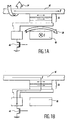
- the junction bears the reference 2. It is a stack comprising a sandwich oxide layer between two magnetic layers. This system works like a spin valve, except that the current flows perpendicular to the planes of the layers.
- One of the magnetic layers is called “free” because its magnetization can be oriented in a magnetic field exterior (bidirectional arrow); the other is said “trapped” because its direction of magnetization is fixed by an antiferromagnetic exchange layer (arrow unidirectional).
- the magnetizations of magnetic layers are antiparallel, resistance of the junction is high; when the magnetizations are parallel, the resistance becomes weak. The relative variation of resistance between these two states can reach 40% by an appropriate choice of materials.
- junction 2 is placed between a transistor switching 4 and a current supply line 6. A current flowing through it produces a field magnetic 7.
- the transistor In the "read” mode (Fig. 1B), the transistor is placed in saturated mode (i.e. the current crossing is maximum) by sending an impulse positive current in the base.
- the current sent in line 6 crosses only the memory point whose transistor is open. This current allows measure the resistance of the junction. By comparing with a reference memory point, the state of the point memory (“O" or "1") can thus be determined.
- the purpose of the present invention is to remedy these drawbacks.
- the invention aims to reduce the critical density of current from which the flipping of the magnetization occurs in the free layer.
- the work and reflections of the Applicant have enabled understand that this critical density was linked to the demagnetizing field specific to the free layer.
- the invention therefore proposes a device in which this demagnetizing field is very weak, even zero.
- we use a three-layer stack (that we will call hereafter “three-layer stacking” or simply “tri-layer") formed of two layers magnetic separated by a conductive layer not magnetic, the latter having a thickness sufficiently weak that the coupling between the two magnetic layers is strong enough that the magnetizations in these layers are antiparallel. Overall, such a system has little or no demagnetizing field.
- the Applicant qualifies such stacks of "synthetics".
- the trapped layer is, also made up of a three-layer stack, this second stack being covered with a layer antiferromagnetic exchange setting the direction of magnetizations in said second three-layer stack.
- the device includes a third tri-layer stack separate from the first by a non-magnetic conductive layer, this third three-layer stack based on a second antiferromagnetic exchange layer fixing the magnetizations in this third tri-layer.
- the material of the magnetic layers of the first and / or the second and / or the third stack is preferably made of a material taken from the group consisting of Co, Fe, Ni and their alloys.
- the non-magnetic conductive layer of the first and / or the second and / or the third stack three-layer is preferably made of a metal taken from the group consisting of Ru, Re, Cu, Cr, Pt, Ag.
- the first and / or second layer antiferromagnetic can be Mn-based alloy (e.g. FeMn, IrMn, NiMn, PtMn, PtPdMn, RuRhMn).
- Mn-based alloy e.g. FeMn, IrMn, NiMn, PtMn, PtPdMn, RuRhMn.
- a electric current flowing in a conductor is made up of electrons whose spin has no reason a a priori to be oriented in a particular direction.
- this current crosses a magnetic layer presenting a particular magnetization, the spins go find themselves oriented by exchange phenomena of magnetic moment, so the electrons will come out of this layer with a polarized spin.
- Such a layer (or a set of such layers) thus constitutes a "Polarizer”.
- This phenomenon can play as well in transmission (through the layer) than in reflection (on this layer), according to the direction of circulation of the current. He can also play in reverse preferably passing electrons with a spin polarized in a certain direction. Function of the layer is then that of an analyzer.
- the first embodiment of the invention consists in using a tunnel junction formed by two tri-layer stacks arranged on either side of an insulating layer, for example made of alumina (Al 2 O 3 ).
- an insulating layer for example made of alumina (Al 2 O 3 ).
- One of the tri-layers has its direction of magnetization fixed by exchange coupling with an antiferromagnetic layer. This layer plays a dual role of polarizer (in writing) and analyzer (in writing and reading).
- the choice of a tri-layer was chosen to eliminate the magnetostatic coupling with the second tri-layer and therefore to be able to use the memory without an external compensation field.
- the other tri-layer is free to orient itself in the direction of polarization of the spins.
- This layer has a planar anisotropy defining an axis of easy and an axis of difficult magnetization in order to reduce the writing time.
- the thicknesses of the magnetic layers of this three-layer system are almost equal in order to eliminate the demagnetizing field effect and therefore allow the magnetization of this layer to precess easily out of the plane.
- a density current greater than the critical density crossing the junction will cause precession and alignment of the magnetization of the free layer (closest to the oxide barrier) by transfer of magnetic moment electrons polarized at the magnetic moment of the free layer.
- the voltage appearing across the junction allows to follow the magnetic state of the free layer. Writing can be done while running continuous or pulsed current, the duration of the pulse to be adjusted according to the process of magnetization reversal.
- Figure 2 illustrates this first mode of production.
- the device includes two tri-layer (or “synthetic") stacks, 12 and 16 respectively, one for the trapped layer (12) and the other for the free layer (16).
- the device comprises successively, from top to bottom, an exchange layer antiferromagnetic 10, the trapped layer 12, a layer non-magnetic insulator 14, the free layer 16, the assembly referenced 18 forming a tunnel junction magnetic. This junction rests on a substrate conductor 20 and is interposed between a conductor 22 and a transistor 24.
- the layer trapped 12 is a tri-layer consisting of two layers magnetic 121, 123 separated by a layer non-magnetic conductor 122.
- the layer free 16 is a tri-layer composed of two layers magnetic 161, 163 separated by a layer non-magnetic conductor 162.
- the magnetizations of the two magnetic layers are antiparallel, as symbolically represented on the figure by arrows of alternate directions, arrows which represent the magnetization. This antiparallelism is due to a very strong antiferromagnetic coupling existing between the magnetic layers.
- the thicknesses magnetic layers 121, 123 are advantageously the same in order to have a zero magnetostatic coupling on the free layer 16.
- the free layer 16 has characteristics similar to the trapped layer 12. However, not being not trapped by exchange, she is free, and sees the direction of its magnetization change when a current spin polarized crosses it. This change is related to transfer of magnetic moment from electrons to the magnetization of the layer.
- the barrier 14 is preferably formed of a oxidized or nitrided aluminum layer, and it's obtained by methods known to those skilled in the art (plasma oxidation, natural in situ oxidation, atomic oxygen source, ). Materials semiconductors can also be used but the magnetoresistive properties are not as good than with nitrides and oxides.
- Figure 3A illustrates the writing of a "O" and FIG. 3B the writing of a "1".
- the different directions are identified with respect to an Oxyz direct triangle, the direction Oz being perpendicular to the plane of the layers.
- Figure 4A shows how the component My of the magnetization of layer 161 changes sign and
- Figure 4B shows the oscillation of the Mz component during the precession movement that accompanies the reversal of the magnetization.
- writing can be done in direct or pulsed current.
- the duration of the pulse must be sufficient long for the turnaround to be complete.
- the turning control can be done by measuring of the voltage across the junction.
- the magnetizations of layers 123 and 161 are parallel, the probability of electron transfer by tunnel effect is high and the resistance of the junction is low. If the turnaround has not been completed completely, resistance is great.
- the magnetic state of the device is determined. In this magnetic state control step, the layer 123 (fixed by exchange) plays the role of analyzer for probe the orientation of the free layer 161.
- the device comprises three tri-layers, two of the tri-layers being arranged on either side of an insulating layer, for example made of alumina (Al 2 O 3 ).
- an insulating layer for example made of alumina (Al 2 O 3 ).
- One of these tri-layers has its magnetization directions fixed by exchange coupling with an antiferromagnetic layer. This layer plays a dual role of polarizer (in writing) and analyzer (in writing and reading).
- the choice of a tri-layer makes it possible to eliminate the magnetostatic coupling on the second tri-layer and therefore to be able to use the memory without an external compensation field.
- the other tri-layer is free to orient itself in the direction of polarization of the spins.
- This layer may have a planar anisotropy defining an axis of easy and an axis of difficult magnetization in order to reduce the writing time.
- the thicknesses of the magnetic layers of this system are almost equal in order to eliminate the demagnetizing field effect.
- the device also comprises a polarizer separated from the tunnel junction by a non-magnetic conductive layer and preferably formed by a tri-layer stack trapped by exchange with an antiferromagnetic layer in order to maintain its direction of magnetization.
- FIG. 5 illustrates this second mode of production.
- the three tri-layers carry references 16, 12 and 32 respectively.
- third tri-layer 32 is separated from the first 16 by a non-magnetic conductive layer 30.
- This third tri-layer includes two magnetic layers 321, 323 separated by a non-magnetic conductive layer 322. It is based on a coupling layer antiferromagnetic 34 which fixes the magnetization in the layer 323, so in layer 321.
- the third tri-layer 32 is therefore of the trapped type, like the second (12).
- the assembly rests on a conductive substrate 36.
- the layer 30 separating the first and the third tri-layers can be formed from a noble metal. Its thickness is chosen between 3 and 10 nm to avoid untimely magnetic couplings between the tri-layers 16 and 32.
- the electrons are always polarized according to (-y) and polarize according to (+ y) after passage in the layer 163, without causing the layer to tip over 163 because of the antiferromagnetic exchange between the layers 161 and 163 which is much higher than the coupling exerted by electrons.
- the majority electrons will accumulate in layers 30 and 163, which will stabilize the orientation of layer 163.
- the polarizer 12 acts by electron transmission polarized while the polarizer 32 acts by reflection of polarized electrons.
- Polarizer 32 eliminates the coupling field magneto-static on layer 16 and also allows to have an identical exchange direction between layers 121 and 323 in order to make possible the setting magnetic order of the antiferromagnetic layers exchange 10 and 34. It is indeed difficult to define two opposite directions of exchange in a system using only one type of material antiferromagnetic.
- the reading is carried out as in the first variant by injecting a current of lower density to the critical density and comparing the voltage read to the voltage of a reference junction.
- Mode of realization 1 2 t (nm) 5 5 Ms (emu / cc) 1500 1500 Hk effective (G) 40 40 Jc (writing) (A / cm 2 ) 3.2E + 05 1.6E + 05 RA max (Ohm. ⁇ m 2 ) 188 375 Pv (reading) (A / cm 2 ) 1.6E + 05 8E + 04 a min (micron) 0.12 0.12
- FIG 7 shows a memory formed of a matrix of memory points addressable by lines and by columns.
- Each memory point includes a device according to the invention, with a stack of layers symbolized by a resistance 60 and a means switching 70 constituted by a transistor.
- Each stack is connected to an address line 80 and the base (or gate) of the single-column transistor address 90.
- Lines 80 are called “lines of bit “and columns 90" word lines "(or digit).
- Lines 80 are connected to the outputs of a circuit address line 85 and columns 90 at the outputs of a column 95 addressing circuit.
- a reference column 100 which allows reading.
- a reading current flows in the memory points of a column 90, we compare the reading voltage of each point with the voltage read on the memory point of the reference column belonging to the same line.
- This column writing and reading mechanism dramatically reduces the cycle time of the memory.
Abstract
Dispositif magnétique à polarisation de spin et à empilement(s) tri-couche(s) et mémoire utilisant ce dispositif. Selon l'invention, le dispositif comprend un empilement tri-couche (16) constituant la couche magnétique libre. Ce tri-couche est formé de deux couches magnétiques (161, 163) séparées par une couche conductrice non magnétique (162). Cet empilement ne présente plus de champ démagnétisant, ce qui réduit la densité critique d'écriture. La couche piégée peut, elle aussi, être constituée d'un tri-couche (12). Application à la réalisation de mémoires magnétiques. <IMAGE>Magnetic device with spin polarization and tri-layer stack (s) and memory using this device. According to the invention, the device comprises a three-layer stack (16) constituting the free magnetic layer. This tri-layer is formed by two magnetic layers (161, 163) separated by a non-magnetic conductive layer (162). This stack no longer has a demagnetizing field, which reduces the critical writing density. The trapped layer can also consist of a tri-layer (12). Application to the production of magnetic memories. <IMAGE>
Description
La présente invention a pour objet un dispositif magnétique à polarisation de spin et à empilement(s) tri-couche(s) et une mémoire utilisant ce dispositif.The present invention relates to a device magnetic with spin polarization and stack (s) tri-layer (s) and a memory using this device.
Elle trouve une application en électronique et notamment dans la réalisation de points mémoire et de mémoire de type MRAM ("Magnetic Random Access Memory" ou mémoire magnétique à accès direct (ou aléatoire)).It finds an application in electronics and especially in the creation of memory points and MRAM ("Magnetic Random Access Memory") type memory or magnetic memory with direct (or random) access).
Les mémoires magnétiques MRAM ont connu un regain d'intérêt avec la mise au point de jonctions tunnel magnétiques (en abrégé MTJ pour "Magnetic Tunnel Junction") présentant une forte magnétorésistance à température ambiante. Les figures 1A et 1B annexées illustrent schématiquement la structure et la fonction d'une telle jonction.MRAM magnetic memories have experienced a revival of interest with the development of tunnel junctions magnetic (abbreviated as MTJ for "Magnetic Tunnel Junction ") with strong magnetoresistance to ambient temperature. Figures 1A and 1B attached schematically illustrate the structure and function of such a junction.
La jonction porte la référence 2. Il s'agit d'un
empilement comprenant une couche d'oxyde en sandwich
entre deux couches magnétiques. Ce système fonctionne
comme une vanne de spin, à la différence que le courant
circule perpendiculairement aux plans des couches.
L'une des couches magnétiques est dite "libre" car son
aimantation peut s'orienter dans un champ magnétique
extérieur (flèche bidirectionnelle) ; l'autre est dite
"piégée" car sa direction d'aimantation est fixée par
une couche d'échange antiferromagnétique (flèche
unidirectionnelle). Lorsque les aimantations des
couches magnétiques sont antiparallèles, la résistance
de la jonction est élevée ; lorsque les aimantations
sont parallèles, la résistance devient faible. La
variation relative de résistance entre ces deux états
peut atteindre 40% par un choix approprié des
matériaux.The junction bears the
La jonction 2 est placée entre un transistor de
commutation 4 et une ligne d'amenée de courant 6. Un
courant passant dans celle-ci produit un champ
magnétique 7. Un conducteur 8, orthogonal à la ligne
d'amenée de courant 6 (c'est-à-dire en l'espèce,
perpendiculaire au plan de la figure) permet de
produire un second champ magnétique 9 (situé dans le
plan de la figure).
Dans le mode "écriture" (Fig. 1A), le transistor 4
est bloqué. Des courants circulent dans l'amenée de
courant 6 et dans le conducteur 8. La jonction 2 est
donc soumise à deux champs magnétiques orthogonaux.
L'un est appliqué selon l'axe de difficile aimantation
de la couche libre, afin de réduire son champ de
retournement, l'autre étant appliqué selon son axe
facile afin de provoquer le retournement de
l'aimantation et l'écriture du point mémoire. Dans le
principe, seul le point mémoire placé à l'intersection
des deux lignes 6 et 8 est susceptible de se retourner,
car chaque champ magnétique pris individuellement n'est
pas suffisamment grand pour provoquer un basculement de
l'aimantation. In the "write" mode (Fig. 1A), the
Dans le mode "lecture" (Fig. 1B), le transistor
est placé en régime saturé (c'est-à-dire que le courant
le traversant est maximum) par l'envoi d'une impulsion
de courant positive dans la base. Le courant envoyé
dans la ligne 6 traverse uniquement le point mémoire
dont le transistor est ouvert. Ce courant permet de
mesurer la résistance de la jonction. Par comparaison
avec un point mémoire de référence, l'état du point
mémoire ("O" ou "1") peut ainsi être déterminé.In the "read" mode (Fig. 1B), the transistor
is placed in saturated mode (i.e. the current
crossing is maximum) by sending an impulse
positive current in the base. The current sent
in
Un tel mécanisme d'écriture présente des
inconvénients en particulier dans un réseau de
jonctions :
Récemment sont apparus d'autres types de
dispositifs magnétiques où le reversement de
l'aimantation se produit non plus par des champs
magnétiques extérieurs mais par des électrons
traversant l'empilement perpendiculairement au plan des
couches. Ces dispositifs sont décrits dans le document
US-A-5,695,864. Le mécanisme mis en oeuvre est fondé
sur un transfert de moment magnétique entre les
électrons d'une part et l'aimantation de la couche
libre, d'autre part. Dans un tel système, l'empilement
est formé de couches toutes conductrices de
l'électricité, afin de limiter la puissance dissipée.
Il en résulte plusieurs inconvénients :
La présente invention a justement pour but de remédier à ces inconvénients.The purpose of the present invention is to remedy these drawbacks.
L'invention vise à réduire la densité critique de courant à partir de laquelle le retournement de l'aimantation se produit dans la couche libre. Les travaux et réflexions du Demandeur ont permis de comprendre que cette densité critique était liée au champ démagnétisant propre à la couche libre. L'invention propose alors un dispositif dans lequel ce champ démagnétisant est très faible, voire nul. Pour cela, on utilise un empilement à trois couches (que l'on appellera par la suite "empilement tri-couche" ou simplement "tri-couche") formé de deux couches magnétiques séparées par une couche conductrice non magnétique, cette dernière ayant une épaisseur suffisamment faible pour que le couplage entre les deux couches magnétiques soit suffisamment fort pour que les aimantations dans ces couches soient antiparallèles. Globalement, un tel système ne présente pas (ou peu) de champ démagnétisant. Le Demandeur qualifie de tels empilements de "synthétiques". The invention aims to reduce the critical density of current from which the flipping of the magnetization occurs in the free layer. The work and reflections of the Applicant have enabled understand that this critical density was linked to the demagnetizing field specific to the free layer. The invention therefore proposes a device in which this demagnetizing field is very weak, even zero. For this, we use a three-layer stack (that we will call hereafter "three-layer stacking" or simply "tri-layer") formed of two layers magnetic separated by a conductive layer not magnetic, the latter having a thickness sufficiently weak that the coupling between the two magnetic layers is strong enough that the magnetizations in these layers are antiparallel. Overall, such a system has little or no demagnetizing field. The Applicant qualifies such stacks of "synthetics".
De façon précise, l'invention a donc pour objet un dispositif magnétique comprenant :
- une première couche magnétique dite "piégée" ayant une aimantation de direction fixe,
- une seconde couche magnétique dite "libre" ayant une aimantation de direction variable,
- une couche isolante ou semi-conductrice séparant la couche piégée et la couche libre,
- des moyens pour faire circuler dans les couches et perpendiculairement à celles-ci un courant d'électrons,
- des moyens de polarisation du spin de ces électrons,
- a first magnetic layer called "trapped" having a fixed direction magnetization,
- a second magnetic layer called "free" having a magnetization of variable direction,
- an insulating or semiconductive layer separating the trapped layer and the free layer,
- means for circulating in the layers and perpendicular to them a current of electrons,
- means for polarizing the spin of these electrons,
Dans un mode de réalisation, la couche piégée est, elle aussi constituée d'un empilement tri-couche, ce deuxième empilement étant recouvert d'une couche d'échange antiferromagnétique fixant la direction des aimantations dans ledit deuxième empilement tri-couche.In one embodiment, the trapped layer is, also made up of a three-layer stack, this second stack being covered with a layer antiferromagnetic exchange setting the direction of magnetizations in said second three-layer stack.
Dans un autre mode de réalisation, le dispositif comprend un troisième empilement tri-couche séparé du premier par une couche conductrice non magnétique, ce troisième empilement tri-couche reposant sur une seconde couche d'échange antiferromagnétique fixant les aimantations dans ce troisième tri-couche.In another embodiment, the device includes a third tri-layer stack separate from the first by a non-magnetic conductive layer, this third three-layer stack based on a second antiferromagnetic exchange layer fixing the magnetizations in this third tri-layer.
Le matériau des couches magnétiques du premier et/ou du deuxième et/ou du troisième empilement tricouche est de préférence en un matériau pris dans le groupe constitué par Co, Fe, Ni et leurs alliages.The material of the magnetic layers of the first and / or the second and / or the third stack is preferably made of a material taken from the group consisting of Co, Fe, Ni and their alloys.
La couche conductrice non magnétique du premier et/ou du deuxième et/ou du troisième empilement tricouche est de préférence en un métal pris dans le groupe constitué par Ru, Re, Cu, Cr, Pt, Ag.The non-magnetic conductive layer of the first and / or the second and / or the third stack three-layer is preferably made of a metal taken from the group consisting of Ru, Re, Cu, Cr, Pt, Ag.
La première et/ou la seconde couche antiferromagnétique peut être en alliage à base de Mn (par exemple FeMn, IrMn, NiMn, PtMn, PtPdMn, RuRhMn).The first and / or second layer antiferromagnetic can be Mn-based alloy (e.g. FeMn, IrMn, NiMn, PtMn, PtPdMn, RuRhMn).
- les figures 1A et 1B, déjà décrites, montrent un dispositif connu pour l'écriture et la lecture d'une information binaire dans une jonction magnétique à effet tunnel par des champs magnétiques extérieurs ;Figures 1A and 1B, already described, show a known device for writing and reading binary information in a magnetic tunnel junction by external magnetic fields;
- la figure 2 montre, en coupe, un premier mode de réalisation d'un dispositif selon l'invention ;Figure 2 shows, in section, a first mode production of a device according to the invention;
- les figures 3A et 3B montrent les orientations des aimantations dans les différentes couches selon qu'on a écrit un "0" ou un "1" pour ce premier mode de réalisation ;Figures 3A and 3B show the orientations magnetizations in the different layers depending on whether you wrote a "0" or a "1" for this first embodiment;
- les figures 4A et 4B montrent les variations transitoires de la composante de l'aimantation selon un axe Oz perpendiculaire au plan des couches et selon un axe Oy parallèle au plan des couches, pour une faible et une forte anisotropie ;Figures 4A and 4B show the variations transients of the magnetization component along an axis Oz perpendicular to the plane of layers and along an axis Oy parallel to the plane layers, for weak and strong anisotropy ;
- la figure 5 montre, en coupe, un second mode de réalisation d'un dispositif selon l'invention ; FIG. 5 shows, in section, a second mode of production of a device according to the invention;
- les figures 6A et 6B montrent les orientations des aimantations dans les différentes couches selon qu'on a écrit un "O" ou un "1", pour ce second mode de réalisation ;Figures 6A and 6B show the orientations magnetizations in the different layers depending on whether you wrote an "O" or a "1", for this second embodiment;
- la figure 7 montre schématiquement une mémoire utilisant une matrice de dispositifs selon l'invention.Figure 7 schematically shows a memory using a matrix of devices according to the invention.
A propos du phénomène de polarisation de spin pour des électrons circulant dans des dispositifs à jonction tunnel, on peut rappeler les principes suivants. Un courant électrique circulant dans un conducteur est constitué d'électrons dont le spin n'a aucune raison a priori d'être orienté dans une direction particulière. Lorsque ce courant traverse une couche magnétique présentant une aimantation particulière, les spins vont se trouver orientés par des phénomènes d'échange de moment magnétique, de sorte que les électrons sortiront de cette couche avec un spin polarisé. Une telle couche (ou un ensemble de telles couches) constitue ainsi un "polariseur". Ce phénomène peut jouer aussi bien en transmission (à travers la couche) qu'en réflexion (sur cette couche), selon la direction de circulation du courant. Il peut également jouer en sens inverse en laissant passer de préférence des électrons ayant un spin polarisé dans une certaine direction. La fonction de la couche est alors celle d'un analyseur.About the spin polarization phenomenon for electrons flowing in junction devices tunnel, we can recall the following principles. A electric current flowing in a conductor is made up of electrons whose spin has no reason a a priori to be oriented in a particular direction. When this current crosses a magnetic layer presenting a particular magnetization, the spins go find themselves oriented by exchange phenomena of magnetic moment, so the electrons will come out of this layer with a polarized spin. Such a layer (or a set of such layers) thus constitutes a "Polarizer". This phenomenon can play as well in transmission (through the layer) than in reflection (on this layer), according to the direction of circulation of the current. He can also play in reverse preferably passing electrons with a spin polarized in a certain direction. Function of the layer is then that of an analyzer.
S'agissant maintenant du premier mode de réalisation de l'invention, il consiste à utiliser une jonction tunnel formée de deux empilements tri-couches disposés de part et d'autre d'une couche isolante, par exemple en alumine (Al2O3). Un des tri-couches a sa direction d'aimantation fixée par couplage d'échange avec une couche antiferromagnétique. Cette couche joue un double rôle de polariseur (à l'écriture) et d'analyseur (à l'écriture et la lecture). Le choix d'un tri-couche a été retenu pour éliminer le couplage magnétostatique avec le second tri-couche et donc pour pouvoir utiliser la mémoire sans champ extérieur de compensation. L'autre tri-couche est libre de s'orienter dans la direction de polarisation des spins.. Cette couche possède une anisotropie planaire définissant un axe de facile et un axe de difficile aimantation afin de réduire le temps d'écriture. Les épaisseurs des couches magnétiques de ce système tricouche sont quasiment égales afin d'éliminer l'effet de champ démagnétisant et donc permettre l'aimantation de cette couche de précessionner facilement hors du plan.Turning now to the first embodiment of the invention, it consists in using a tunnel junction formed by two tri-layer stacks arranged on either side of an insulating layer, for example made of alumina (Al 2 O 3 ). One of the tri-layers has its direction of magnetization fixed by exchange coupling with an antiferromagnetic layer. This layer plays a dual role of polarizer (in writing) and analyzer (in writing and reading). The choice of a tri-layer was chosen to eliminate the magnetostatic coupling with the second tri-layer and therefore to be able to use the memory without an external compensation field. The other tri-layer is free to orient itself in the direction of polarization of the spins. This layer has a planar anisotropy defining an axis of easy and an axis of difficult magnetization in order to reduce the writing time. The thicknesses of the magnetic layers of this three-layer system are almost equal in order to eliminate the demagnetizing field effect and therefore allow the magnetization of this layer to precess easily out of the plane.
Dans le mode écriture, un courant de densité supérieure à la densité critique traversant la jonction va provoquer une précession et un alignement de l'aimantation de la couche libre (la plus proche de la barrière d'oxyde) par transfert du moment magnétique des électrons polarisés au moment magnétique de la couche libre. La tension apparaissant aux bornes de la jonction, permet de suivre l'état magnétique de la couche libre. L'écriture peut se faire en courant continu ou en courant pulsé, la durée de l'impulsion devant être ajustée en fonction du processus de retournement de l'aimantation. In write mode, a density current greater than the critical density crossing the junction will cause precession and alignment of the magnetization of the free layer (closest to the oxide barrier) by transfer of magnetic moment electrons polarized at the magnetic moment of the free layer. The voltage appearing across the junction, allows to follow the magnetic state of the free layer. Writing can be done while running continuous or pulsed current, the duration of the pulse to be adjusted according to the process of magnetization reversal.
Dans le mode lecture, un courant de densité inférieure à la densité critique traverse la jonction et permet de lire l'état magnétique du dispositif, lequel se comporte ainsi comme un point mémoire.In reading mode, a density current below the critical density crosses the junction and makes it possible to read the magnetic state of the device, which thus behaves like a memory point.
La figure 2 illustre ce premier mode de
réalisation. Tel que représenté, le dispositif comprend
deux empilements tri-couches (ou "synthétiques"),
respectivement 12 et 16, l'un pour la couche piégée
(12) et l'autre pour la couche libre (16). Dans la
variante illustrée, le dispositif comprend
successivement, de haut en bas, une couche d'échange
antiferromagnétique 10, la couche piégée 12, une couche
isolante non magnétique 14, la couche libre 16,
l'ensemble référencé 18 formant une jonction tunnel
magnétique. Cette jonction repose sur un substrat
conducteur 20 et se trouve intercalé entre un
conducteur 22 et un transistor 24.Figure 2 illustrates this first mode of
production. As shown, the device includes
two tri-layer (or "synthetic") stacks,
12 and 16 respectively, one for the trapped layer
(12) and the other for the free layer (16). In the
illustrated variant, the device comprises
successively, from top to bottom, an exchange layer
antiferromagnetic 10, the trapped
Selon le mode de réalisation illustré, la couche
piégée 12 est un tri-couche composé de deux couches
magnétiques 121, 123 séparées par une couche
conductrice non magnétique 122. De même, la couche
libre 16 est un tri-couche composé de deux couches
magnétiques 161, 163 séparées par une couche
conductrice non magnétique 162.According to the illustrated embodiment, the layer
trapped 12 is a tri-layer consisting of two layers
magnetic 121, 123 separated by a layer
Dans les deux tri-couches 12 et 16, les
aimantations des deux couches magnétiques sont
antiparallèles, comme représenté symboliquement sur la
figure par les flèches de directions alternées, flèches
qui représentent l'aimantation. Cet antiparallélisme
est dû à un couplage antiferromagnétique très fort
existant entre les couches magnétiques. Les épaisseurs
des couches magnétiques 121, 123 sont avantageusement
les mêmes afin d'avoir un couplage magnétostatique nul
sur la couche libre 16.In the two tri-layers 12 and 16, the
magnetizations of the two magnetic layers are
antiparallel, as symbolically represented on the
figure by arrows of alternate directions, arrows
which represent the magnetization. This antiparallelism
is due to a very strong antiferromagnetic coupling
existing between the magnetic layers. The thicknesses
La couche libre 16 a des caractéristiques
similaires à la couche piégée 12. Cependant, n'étant
pas piégée par échange, elle est libre, et voit la
direction de son aimantation changer lorsqu'un courant
polarisé en spin la traverse. Ce changement est lié au
transfert de moment magnétique des électrons vers
l'aimantation de la couche.The
La barrière 14 est formée préférentiellement d'une
couche d'aluminium oxydée ou nitrurée, et elle est
obtenue par des méthodes connues de l'homme de l'art
(oxydation par plasma, oxydation naturelle in situ,
source d'oxygène atomique, ...). Des matériaux
semi-conducteurs peuvent aussi être employés mais les
propriétés magnétorésistives ne sont pas aussi bonnes
qu'avec les nitrures et oxydes.The
La figure 3A permet d'illustrer l'écriture d'un
"O" et la figure 3B l'écriture d'un "1". Sur ces
figures, on n'a pas représenté l'amenée de courant ni
le transistor. Les différentes directions sont repérées
par rapport à un trièdre trirectangle Oxyz, la
direction Oz étant perpendiculaire au plan des couches.
Par ailleurs, la figure 4A montre comment la composante
My de l'aimantation de la couche 161 change de signe et
la figure 4B montre l'oscillation de la composante Mz
lors du mouvement de précession qui accompagne le
renversement de l'aimantation. Figure 3A illustrates the writing of a
"O" and FIG. 3B the writing of a "1". On these
Figures, we did not represent the current supply nor
the transistor. The different directions are identified
with respect to an Oxyz direct triangle, the
direction Oz being perpendicular to the plane of the layers.
Furthermore, Figure 4A shows how the component
My of the magnetization of
Pour écrire un "0", on fait circuler dans
l'empilement un courant (continu ou pulsé) de signe
positif, c'est-à-dire circulant de haut en bas (donc
vers le transistor). Les électrons voient leur spin
polarisé dans la couche 123 selon la direction (-y).
Ils vont transmettre leur moment magnétique aux moments
de la couche 161 dont l'aimantation va s'aligner
parallèlement à celle de la couche 123. La couche 163,
couplée antiparallèlement à la couche 161, va donc
aussi se réorienter. Lors du transfert de moment
magnétique, l'aimantation de la couche 161 va entrer en
précession autour de l'axe (-y) avec une composante Mz
qui va osciller au cours du temps, comme le montre la
figure 4B. Lorsque l'angle du cône de précession
dépassera 90°, le sens de rotation s'inversera et
l'aimantation se réalignera selon (+y). Le nombre de
précessions nécessaire au retournement dépend de
l'anisotropie de la couche dans son plan. Lorsque
l'anisotropie est faible (courbes 30 et 32), le
retournement demande un grand nombre d'oscillations de
précessions mais un faible courant critique. Pour une
plus forte anisotropie (courbes 31 et 34) le temps de
retournement est plus court mais un courant plus fort
est nécessaire pour vaincre l'anisotropie.To write a "0", we circulate in
stacking a sign (continuous or pulsed) current
positive, i.e. flowing from top to bottom (therefore
to the transistor). The electrons see their spin
polarized in
Comme dit précédemment, l'écriture peut se faire
en courant continu ou pulsé. Dans le cas d'un courant
pulsé, la durée de l'impulsion doit être suffisamment
longue pour que le retournement soit complet. Le
contrôle du retournement peut s'effectuer par la mesure
de la tension aux bornes de la jonction. Lorsque les
aimantations des couches 123 et 161 sont parallèles, la
probabilité de transfert des électrons par effet tunnel
est grande et la résistance de la jonction est faible.
Si le retournement ne s'est pas effectué complètement,
la résistance est grande. Par comparaison avec la
tension prise aux bornes d'une jonction de référence,
on détermine l'état magnétique du dispositif. Dans
cette étape de contrôle de l'état magnétique, la couche
123 (fixée par échange) joue le rôle d'analyseur pour
sonder l'orientation de la couche libre 161.As said before, writing can be done
in direct or pulsed current. In the case of a current
pulsed, the duration of the pulse must be sufficient
long for the turnaround to be complete. The
turning control can be done by measuring
of the voltage across the junction. When the
magnetizations of
Pour écrire un "1", on fait circuler un courant de
signe négatif comme le montre la figure 3B. En partant
de l'état "0", les électrons majoritaires polarisés
dans la couche 161 selon (-y) vont traverser la couche
123, alors que les électrons minoritaires polarisés
selon (+y) vont s'accumuler devant la couche 123. Ces
électrons de spins antiparallèles à la couche 161 vont
transférer leur moment magnétique aux moments de la
couche 41 et provoquer une précession jusqu'au
retournement de l'aimantation de la couche 161 comme
montré sur la figure 3B. Cette configuration magnétique
correspond à l'écriture d'un "1" et la résistance de la
jonction est maximum.To write a "1", a current of
negative sign as shown in Figure 3B. Starting
of state "0", the majority polarized electrons
in
Pour la lecture, on envoie un courant dont la densité est inférieure à la densité critique et on compare la tension de sortie à la tension d'une jonction de référence, afin de déterminer l'état magnétique du dispositif.For reading, we send a current whose density is below the critical density and we compare the output voltage to the voltage of a reference junction, to determine the state magnetic device.
Dans un second mode de réalisation, le dispositif comprend trois tri-couches, deux des tri-couches étant disposés de part et d'autre d'une couche isolante, par exemple en alumine (Al2O3). L'un de ces tri-couches a ses directions d'aimantation fixées par couplage d'échange avec une couche antiferromagnétique. Cette couche joue un double rôle de polariseur (à l'écriture) et d'analyseur (à l'écriture et la lecture). Le choix d'un tri-couche permet d'éliminer le couplage magnétostatique sur le second tri-couche et donc de pouvoir utiliser la mémoire sans champ extérieur de compensation. L'autre tri-couche est libre de s'orienter dans la direction de polarisation des spins. Cette couche peut posséder une anisotropie planaire définissant un axe de facile et un axe de difficile aimantation afin de réduire le temps d'écriture. Les épaisseurs des couches magnétiques de ce système sont quasiment égales afin d'éliminer l'effet de champ démagnétisant. Le dispositif comprend encore un polariseur séparé de la jonction tunnel par une couche conductrice non magnétique et formé préférentiellement d'un empilement tri-couche piégé par échange avec une couche antiferromagnétique afin de maintenir sa direction d'aimantation.In a second embodiment, the device comprises three tri-layers, two of the tri-layers being arranged on either side of an insulating layer, for example made of alumina (Al 2 O 3 ). One of these tri-layers has its magnetization directions fixed by exchange coupling with an antiferromagnetic layer. This layer plays a dual role of polarizer (in writing) and analyzer (in writing and reading). The choice of a tri-layer makes it possible to eliminate the magnetostatic coupling on the second tri-layer and therefore to be able to use the memory without an external compensation field. The other tri-layer is free to orient itself in the direction of polarization of the spins. This layer may have a planar anisotropy defining an axis of easy and an axis of difficult magnetization in order to reduce the writing time. The thicknesses of the magnetic layers of this system are almost equal in order to eliminate the demagnetizing field effect. The device also comprises a polarizer separated from the tunnel junction by a non-magnetic conductive layer and preferably formed by a tri-layer stack trapped by exchange with an antiferromagnetic layer in order to maintain its direction of magnetization.
La figure 5 illustre ce second mode de
réalisation. Les trois tri-couches portent
respectivement les références 16, 12 et 32. Le
troisième tri-couche 32 est séparé du premier 16 par
une couche conductrice non magnétique 30. Ce troisième
tri-couche comprend deux couches magnétiques 321, 323
séparées par une couche conductrice non magnétique 322.
Il repose sur une couche de couplage
antiferromagnétique 34 qui fixe l'aimantation dans la
couche 323, donc dans la couche 321. Le troisième
tri-couche 32 est donc du type piégé, comme le deuxième
(12). L'ensemble repose sur un substrat conducteur 36.Figure 5 illustrates this second mode of
production. The three tri-layers carry
La couche 30 séparant le premier et le troisième
tri-couches peut être formée à partir d'un métal noble.
Son épaisseur est choisie entre 3 et 10 nm pour éviter
des couplages magnétiques intempestifs entre les
tri-couches 16 et 32.The
L'écriture des états magnétiques "1" et "O"
s'effectue, comme précédemment, par le choix de
l'orientation du sens du courant comme le montrent les
figures 6A et 6B. L'ajout du troisième tri-couche 32 va
stabiliser les états magnétiques et permettre ainsi de
réduire la densité de courant critique d'un facteur 2.
Dans le cas de l'écriture d'un "0" (figure 6A), le
courant polarisé dans la courbe 123 selon (-y) (par
rapport à un même trièdre trirectangle Oxyz non
représenté) va provoquer l'alignement de la couche 161
par transfert du moment des électrons vers
l'aimantation de la couche 161. En sortie de la couche
161, les électrons sont toujours polarisés selon (-y)
et se polarisent selon (+y) après passage dans la
couche 163, sans provoquer de basculement de la couche
163 à cause de l'échange antiferromagnétique entre les
couches 161 et 163 qui est très supérieur au couplage
exercé par les électrons. En arrivant au niveau de la
couche 321, les électrons majoritaires vont s'accumuler
dans les couches 30 et 163, ce qui stabilisera
l'orientation de la couche 163. On peut donc considérer
que le polariseur 12 agit par transmission d'électrons
polarisés alors que le polariseur 32 agit par réflexion
d'électrons polarisés. The writing of the magnetic states "1" and "O"
is carried out, as before, by the choice of
the direction of the current direction as shown by
Figures 6A and 6B. The addition of the third tri-layer 32 will
stabilize the magnetic states and thus allow
reduce the critical current density by a factor of 2.
In the case of writing a "0" (Figure 6A), the
current polarized in
Pour l'écriture d'un "1", les rôles des polariseurs sont inversés, mais les effets de stabilisation et d'abaissement de la densité critique demeurent.For the writing of a "1", the roles of polarizers are reversed but the effects of stabilization and lowering of the critical density remain.
Le polariseur 32 élimine le champ de couplage
magnéto-statique sur la couche 16 et permet aussi
d'avoir une direction d'échange identique entre les
couches 121 et 323 afin de rendre possible la mise en
ordre magnétique des couches antiferromagnétiques
d'échange 10 et 34. Il est en effet difficile de
définir deux directions d'échange opposées dans un
système utilisant un seul type de matériau
antiferromagnétique.
La lecture s'effectue comme dans la première variante en injectant un courant de densité inférieure à la densité critique et en comparant la tension lue à la tension d'une jonction de référence.The reading is carried out as in the first variant by injecting a current of lower density to the critical density and comparing the voltage read to the voltage of a reference junction.
Les deux modes de réalisation qui viennent d'être décrits peuvent être comparés dans le tableau ci-dessous, où :
- t est l'épaisseur de la couche magnétique à retourner,
- Ms est l'aimantation à saturation de la couche à retourner, dans le cas de CoFe (Ms=1500 emu/cc)),
- Hk est l'anisotropie de la couche magnétique à retourner,
- Jc (écriture) est la densité de courant pour écrire un point mémoire,
- RAmax est le produit de la résistance par la surface de la jonction tunnel, défini de telle façon que la tension à l'écriture n'excède pas 0,6 V,
- Jc (lecture) est la densité de courant pour une tension de lecture de 0,3 V avec RAmax,
- amin est la taille minimale d'un côté du point mémoire (pour un point mémoire carré) avant d'atteindre la limite superparamagnétique.
- t is the thickness of the magnetic layer to be returned,
- Ms is the saturation magnetization of the layer to be returned, in the case of CoFe (Ms = 1500 emu / cc)),
- Hk is the anisotropy of the magnetic layer to be returned,
- Jc (write) is the current density to write a memory point,
- RA max is the product of resistance by the surface of the tunnel junction, defined in such a way that the writing voltage does not exceed 0.6 V,
- Jc (reading) is the current density for a reading voltage of 0.3 V with max RA,
- a min is the minimum size of one side of the memory point (for a square memory point) before reaching the superparamagnetic limit.
La valeur de amin est calculée d'après la formule :
On voit, d'après ce tableau, qu'avec l'invention on peut atteindre de faibles densités de courant d'écriture, compatibles avec des jonctions de produit RA raisonnables (>100 Ω.µm2). De tels produits RA peuvent être obtenus, soit par oxydation plasma, soit et de préférence par oxydation naturelle in situ. It can be seen from this table that, with the invention, low write current densities can be achieved, compatible with reasonable RA product junctions (> 100 Ω.µm 2 ). Such RA products can be obtained either by plasma oxidation, or and preferably by natural oxidation in situ.
La figure 7, enfin, montre une mémoire formée
d'une matrice de points mémoires adressables par lignes
et par colonnes. Chaque point mémoire comprend un
dispositif conforme à l'invention, avec un empilement
de couches symbolisé par une résistance 60 et un moyen
de commutation 70 constitué par un transistor. Chaque
empilement est relié à une ligne d'adressage 80 et la
base (ou la porte) du transistor à une colonne
d'adressage 90. Les lignes 80 sont dites "lignes de
bit" et les colonnes 90 "lignes de mot" (ou de digit).
Les lignes 80 sont reliées aux sorties d'un circuit
d'adressage ligne 85 et les colonnes 90 aux sorties
d'un circuit d'adressage colonne 95.Figure 7, finally, shows a memory formed
of a matrix of memory points addressable by lines
and by columns. Each memory point includes a
device according to the invention, with a stack
of layers symbolized by a
Lorsqu'une séquence de bits doit être écrite (par exemple 100110), on commande l'adressage d'une colonne par une impulsion apte à ouvrir les transistors de la colonne en question et l'on envoie sur chaque ligne une impulsion de courant ayant une polarité appropriée (dans l'exemple pris respectivement +--++-). Tous les bits se trouvent ainsi écrits dans la colonne de cette mémoire, simultanément.When a bit sequence must be written (for example example 100110), the addressing of a column is controlled by an impulse able to open the transistors of the column in question and we send on each line a current pulse with appropriate polarity (in the example taken respectively + - ++ -). All bits are thus written in the column of this memory, simultaneously.
Cet adressage multiple est possible grâce à l'invention puisque, comme expliqué dans l'introduction, un point mémoire peut être écrit sans risque d'écriture intempestive sur les points voisins.This multiple addressing is possible thanks to the invention since, as explained in the introduction, a memory point can be written without risk of untimely writing on neighboring points.
Quelque part dans la mémoire, par exemple au
centre, se trouve une colonne de référence 100, qui
permet la lecture. Lorsqu'un courant de lecture circule
dans les points mémoires d'une colonne 90, on compare
la tension de lecture de chaque point avec la tension
lue sur le point mémoire de la colonne de référence
appartenant à la même ligne.Somewhere in memory, for example at
center, there is a
Ce mécanisme d'écriture et de lecture par colonne réduit considérablement le temps de cycle de la mémoire.This column writing and reading mechanism dramatically reduces the cycle time of the memory.
Claims (11)
Applications Claiming Priority (2)
| Application Number | Priority Date | Filing Date | Title |
|---|---|---|---|
| FR0015895A FR2817999B1 (en) | 2000-12-07 | 2000-12-07 | MAGNETIC DEVICE WITH POLARIZATION OF SPIN AND A STRIP (S) TRI-LAYER (S) AND MEMORY USING THE DEVICE |
| FR0015895 | 2000-12-07 |
Publications (2)
| Publication Number | Publication Date |
|---|---|
| EP1223585A1 true EP1223585A1 (en) | 2002-07-17 |
| EP1223585B1 EP1223585B1 (en) | 2008-04-16 |
Family
ID=8857352
Family Applications (1)
| Application Number | Title | Priority Date | Filing Date |
|---|---|---|---|
| EP01403132A Expired - Lifetime EP1223585B1 (en) | 2000-12-07 | 2001-12-05 | Tri-layer stack spin polarised magnetic device and memory using the same |
Country Status (5)
| Country | Link |
|---|---|
| US (1) | US6603677B2 (en) |
| EP (1) | EP1223585B1 (en) |
| JP (2) | JP4398127B2 (en) |
| DE (1) | DE60133622T2 (en) |
| FR (1) | FR2817999B1 (en) |
Cited By (2)
| Publication number | Priority date | Publication date | Assignee | Title |
|---|---|---|---|---|
| WO2004038723A2 (en) * | 2002-10-22 | 2004-05-06 | Btg International Limited | Magnetic memory device |
| EP1418620A2 (en) * | 2002-11-07 | 2004-05-12 | Samsung Electronics Co., Ltd. | MRAM and methods for manufacturing and driving the same |
Families Citing this family (298)
| Publication number | Priority date | Publication date | Assignee | Title |
|---|---|---|---|---|
| JPS6093175A (en) * | 1983-10-27 | 1985-05-24 | Nippon Denso Co Ltd | Injection timing detector of fuel injection timing regulator |
| DE10059181C2 (en) * | 2000-11-29 | 2002-10-24 | Infineon Technologies Ag | Integrated magnetoresistive semiconductor memory and manufacturing process therefor |
| US6785092B2 (en) * | 2001-07-24 | 2004-08-31 | Seagate Technology Llc | White head for high anisotropy media |
| JP4780878B2 (en) * | 2001-08-02 | 2011-09-28 | ルネサスエレクトロニクス株式会社 | Thin film magnetic memory device |
| FR2832542B1 (en) * | 2001-11-16 | 2005-05-06 | Commissariat Energie Atomique | MAGNETIC DEVICE WITH MAGNETIC TUNNEL JUNCTION, MEMORY AND METHODS OF WRITING AND READING USING THE DEVICE |
| JP3866567B2 (en) * | 2001-12-13 | 2007-01-10 | 株式会社東芝 | Semiconductor memory device and manufacturing method thereof |
| JP3583102B2 (en) * | 2001-12-27 | 2004-10-27 | 株式会社東芝 | Magnetic switching element and magnetic memory |
| US6606262B2 (en) * | 2002-01-10 | 2003-08-12 | Hewlett-Packard Development Company, L.P. | Magnetoresistive random access memory (MRAM) with on-chip automatic determination of optimized write current method and apparatus |
| US6714444B2 (en) | 2002-08-06 | 2004-03-30 | Grandis, Inc. | Magnetic element utilizing spin transfer and an MRAM device using the magnetic element |
| JP4146202B2 (en) * | 2002-09-24 | 2008-09-10 | 株式会社東芝 | Spin tunnel transistor, magnetic reproducing head, magnetic information reproducing system, and magnetic storage device |
| US6838740B2 (en) * | 2002-09-27 | 2005-01-04 | Grandis, Inc. | Thermally stable magnetic elements utilizing spin transfer and an MRAM device using the magnetic element |
| US6958927B1 (en) | 2002-10-09 | 2005-10-25 | Grandis Inc. | Magnetic element utilizing spin-transfer and half-metals and an MRAM device using the magnetic element |
| JP4102280B2 (en) * | 2002-10-14 | 2008-06-18 | 三星電子株式会社 | Magnetic medium using spin-polarized electrons, information recording apparatus and recording method for magnetic medium |
| US6791867B2 (en) * | 2002-11-18 | 2004-09-14 | Hewlett-Packard Development Company, L.P. | Selection of memory cells in data storage devices |
| US6956766B2 (en) * | 2002-11-26 | 2005-10-18 | Kabushiki Kaisha Toshiba | Magnetic cell and magnetic memory |
| JP2004179483A (en) * | 2002-11-28 | 2004-06-24 | Hitachi Ltd | Nonvolatile magnetic memory |
| JP2011171756A (en) * | 2002-12-13 | 2011-09-01 | Japan Science & Technology Agency | Spin injection device and magnetic device using the same |
| JP4873338B2 (en) * | 2002-12-13 | 2012-02-08 | 独立行政法人科学技術振興機構 | Spin injection device and magnetic apparatus using the same |
| US7190611B2 (en) * | 2003-01-07 | 2007-03-13 | Grandis, Inc. | Spin-transfer multilayer stack containing magnetic layers with resettable magnetization |
| US6829161B2 (en) * | 2003-01-10 | 2004-12-07 | Grandis, Inc. | Magnetostatically coupled magnetic elements utilizing spin transfer and an MRAM device using the magnetic element |
| US6847547B2 (en) * | 2003-02-28 | 2005-01-25 | Grandis, Inc. | Magnetostatically coupled magnetic elements utilizing spin transfer and an MRAM device using the magnetic element |
| US6952364B2 (en) * | 2003-03-03 | 2005-10-04 | Samsung Electronics Co., Ltd. | Magnetic tunnel junction structures and methods of fabrication |
| KR100615600B1 (en) * | 2004-08-09 | 2006-08-25 | 삼성전자주식회사 | High density magnetic random access memory device and method of fabricating the smae |
| KR100542743B1 (en) * | 2003-04-22 | 2006-01-11 | 삼성전자주식회사 | Magnetic random access memory |
| US6933155B2 (en) * | 2003-05-21 | 2005-08-23 | Grandis, Inc. | Methods for providing a sub .15 micron magnetic memory structure |
| US7006375B2 (en) * | 2003-06-06 | 2006-02-28 | Seagate Technology Llc | Hybrid write mechanism for high speed and high density magnetic random access memory |
| US6865109B2 (en) * | 2003-06-06 | 2005-03-08 | Seagate Technology Llc | Magnetic random access memory having flux closure for the free layer and spin transfer write mechanism |
| JP4966483B2 (en) * | 2003-06-25 | 2012-07-04 | パナソニック株式会社 | Magnetoresistive element, magnetic head using magnetoresistive element, recording / reproducing apparatus, memory element, memory array, and method for manufacturing magnetoresistive element |
| JP2005064050A (en) * | 2003-08-14 | 2005-03-10 | Toshiba Corp | Semiconductor memory device and method of writing data therein |
| US8755222B2 (en) | 2003-08-19 | 2014-06-17 | New York University | Bipolar spin-transfer switching |
| US6980469B2 (en) * | 2003-08-19 | 2005-12-27 | New York University | High speed low power magnetic devices based on current induced spin-momentum transfer |
| US7573737B2 (en) * | 2003-08-19 | 2009-08-11 | New York University | High speed low power magnetic devices based on current induced spin-momentum transfer |
| US7911832B2 (en) | 2003-08-19 | 2011-03-22 | New York University | High speed low power magnetic devices based on current induced spin-momentum transfer |
| US6985385B2 (en) | 2003-08-26 | 2006-01-10 | Grandis, Inc. | Magnetic memory element utilizing spin transfer switching and storing multiple bits |
| JP2005093488A (en) * | 2003-09-12 | 2005-04-07 | Sony Corp | Magnetoresistive effect element, its manufacturing method, magnetic memory device, and its manufacturing method |
| US7161829B2 (en) * | 2003-09-19 | 2007-01-09 | Grandis, Inc. | Current confined pass layer for magnetic elements utilizing spin-transfer and an MRAM device using such magnetic elements |
| KR100568512B1 (en) * | 2003-09-29 | 2006-04-07 | 삼성전자주식회사 | Magnetic thermal random access memory cells having a heat-generating layer and methods of operating the same |
| KR100615089B1 (en) * | 2004-07-14 | 2006-08-23 | 삼성전자주식회사 | Magnetic random access memory with low switching current |
| KR100835275B1 (en) * | 2004-08-12 | 2008-06-05 | 삼성전자주식회사 | Methods of operating a magnetic random access memory device using a spin injection mechanism |
| US7372722B2 (en) * | 2003-09-29 | 2008-05-13 | Samsung Electronics Co., Ltd. | Methods of operating magnetic random access memory devices including heat-generating structures |
| US7369428B2 (en) * | 2003-09-29 | 2008-05-06 | Samsung Electronics Co., Ltd. | Methods of operating a magnetic random access memory device and related devices and structures |
| JP2005109263A (en) * | 2003-09-30 | 2005-04-21 | Toshiba Corp | Magnetic element and magnetic memory |
| US7027320B2 (en) * | 2003-10-21 | 2006-04-11 | Hewlett-Packard Development Company, L.P. | Soft-reference magnetic memory digitized device and method of operation |
| US7009877B1 (en) | 2003-11-14 | 2006-03-07 | Grandis, Inc. | Three-terminal magnetostatically coupled spin transfer-based MRAM cell |
| US7282755B2 (en) | 2003-11-14 | 2007-10-16 | Grandis, Inc. | Stress assisted current driven switching for magnetic memory applications |
| US7602000B2 (en) * | 2003-11-19 | 2009-10-13 | International Business Machines Corporation | Spin-current switched magnetic memory element suitable for circuit integration and method of fabricating the memory element |
| JP2005166087A (en) * | 2003-11-28 | 2005-06-23 | Toshiba Corp | Semiconductor integrated circuit device |
| JP4581394B2 (en) * | 2003-12-22 | 2010-11-17 | ソニー株式会社 | Magnetic memory |
| US20050136600A1 (en) * | 2003-12-22 | 2005-06-23 | Yiming Huai | Magnetic elements with ballistic magnetoresistance utilizing spin-transfer and an MRAM device using such magnetic elements |
| JP2005209248A (en) * | 2004-01-20 | 2005-08-04 | Hitachi Ltd | Magnetic head, and magnetic recording/reproducing apparatus |
| US7110287B2 (en) | 2004-02-13 | 2006-09-19 | Grandis, Inc. | Method and system for providing heat assisted switching of a magnetic element utilizing spin transfer |
| US7242045B2 (en) | 2004-02-19 | 2007-07-10 | Grandis, Inc. | Spin transfer magnetic element having low saturation magnetization free layers |
| US6967863B2 (en) | 2004-02-25 | 2005-11-22 | Grandis, Inc. | Perpendicular magnetization magnetic element utilizing spin transfer |
| US20110140217A1 (en) * | 2004-02-26 | 2011-06-16 | Grandis, Inc. | Spin transfer magnetic element with free layers having high perpendicular anisotropy and in-plane equilibrium magnetization |
| US6992359B2 (en) | 2004-02-26 | 2006-01-31 | Grandis, Inc. | Spin transfer magnetic element with free layers having high perpendicular anisotropy and in-plane equilibrium magnetization |
| JP2006148039A (en) * | 2004-03-03 | 2006-06-08 | Toshiba Corp | Magneto-resistance effect element and magnetic memory |
| JP2005294376A (en) | 2004-03-31 | 2005-10-20 | Toshiba Corp | Magnetic recording element and magnetic memory |
| US6946698B1 (en) | 2004-04-02 | 2005-09-20 | Taiwan Semiconductor Manufacturing Company, Ltd. | MRAM device having low-k inter-metal dielectric |
| JP4747507B2 (en) * | 2004-04-16 | 2011-08-17 | ソニー株式会社 | Magnetic memory and recording method thereof |
| US7233039B2 (en) * | 2004-04-21 | 2007-06-19 | Grandis, Inc. | Spin transfer magnetic elements with spin depolarization layers |
| US7057921B2 (en) * | 2004-05-11 | 2006-06-06 | Grandis, Inc. | Spin barrier enhanced dual magnetoresistance effect element and magnetic memory using the same |
| US7088609B2 (en) * | 2004-05-11 | 2006-08-08 | Grandis, Inc. | Spin barrier enhanced magnetoresistance effect element and magnetic memory using the same |
| US7576956B2 (en) * | 2004-07-26 | 2009-08-18 | Grandis Inc. | Magnetic tunnel junction having diffusion stop layer |
| KR100660539B1 (en) * | 2004-07-29 | 2006-12-22 | 삼성전자주식회사 | Magnetic memory devices and methods of forming the same |
| US7221584B2 (en) * | 2004-08-13 | 2007-05-22 | Taiwan Semiconductor Manufacturing Company, Ltd. | MRAM cell having shared configuration |
| JP4568152B2 (en) * | 2004-09-17 | 2010-10-27 | 株式会社東芝 | Magnetic recording element and magnetic recording apparatus using the same |
| JP4920881B2 (en) * | 2004-09-27 | 2012-04-18 | 株式会社日立製作所 | Low power consumption magnetic memory and magnetization information writing device |
| JP2006108316A (en) * | 2004-10-04 | 2006-04-20 | Sony Corp | Memory element and memory |
| JP4626253B2 (en) * | 2004-10-08 | 2011-02-02 | ソニー株式会社 | Storage device |
| KR100642638B1 (en) * | 2004-10-21 | 2006-11-10 | 삼성전자주식회사 | Methods of operating a magnetic random access memory device with low critical current density |
| US7149106B2 (en) * | 2004-10-22 | 2006-12-12 | Freescale Semiconductor, Inc. | Spin-transfer based MRAM using angular-dependent selectivity |
| US20060092688A1 (en) * | 2004-10-29 | 2006-05-04 | International Business Machines Corporation | Stacked magnetic devices |
| JP2006165264A (en) * | 2004-12-07 | 2006-06-22 | Sony Corp | Memory, magnetic head, magnetic sensor, and method of manufacturing them |
| JP2006179694A (en) * | 2004-12-22 | 2006-07-06 | Sony Corp | Memory element |
| US7170775B2 (en) * | 2005-01-06 | 2007-01-30 | Taiwan Semiconductor Manufacturing Company, Ltd. | MRAM cell with reduced write current |
| JP2007027197A (en) * | 2005-07-12 | 2007-02-01 | Sony Corp | Storage element |
| JP2007027575A (en) * | 2005-07-20 | 2007-02-01 | Toshiba Corp | Magnetoresistance effect element and magnetic memory |
| JP5096702B2 (en) * | 2005-07-28 | 2012-12-12 | 株式会社日立製作所 | Magnetoresistive element and nonvolatile magnetic memory equipped with the same |
| US7224601B2 (en) | 2005-08-25 | 2007-05-29 | Grandis Inc. | Oscillating-field assisted spin torque switching of a magnetic tunnel junction memory element |
| JP2007081280A (en) * | 2005-09-16 | 2007-03-29 | Fujitsu Ltd | Magnetoresistance effect element and magnetic memory apparatus |
| US7777261B2 (en) * | 2005-09-20 | 2010-08-17 | Grandis Inc. | Magnetic device having stabilized free ferromagnetic layer |
| US7973349B2 (en) * | 2005-09-20 | 2011-07-05 | Grandis Inc. | Magnetic device having multilayered free ferromagnetic layer |
| US7859034B2 (en) * | 2005-09-20 | 2010-12-28 | Grandis Inc. | Magnetic devices having oxide antiferromagnetic layer next to free ferromagnetic layer |
| JP5120699B2 (en) * | 2005-10-03 | 2013-01-16 | 日本電気株式会社 | Magnetic random access memory and operation method thereof |
| US7286395B2 (en) * | 2005-10-27 | 2007-10-23 | Grandis, Inc. | Current driven switched magnetic storage cells having improved read and write margins and magnetic memories using such cells |
| FR2892871B1 (en) * | 2005-11-02 | 2007-11-23 | Commissariat Energie Atomique | SPEED POLARIZED ELELECTIC CURRENT FREQUENCY RADIO OSCILLATOR |
| US7430135B2 (en) * | 2005-12-23 | 2008-09-30 | Grandis Inc. | Current-switched spin-transfer magnetic devices with reduced spin-transfer switching current density |
| US8063459B2 (en) * | 2007-02-12 | 2011-11-22 | Avalanche Technologies, Inc. | Non-volatile magnetic memory element with graded layer |
| US7732881B2 (en) * | 2006-11-01 | 2010-06-08 | Avalanche Technology, Inc. | Current-confined effect of magnetic nano-current-channel (NCC) for magnetic random access memory (MRAM) |
| US8084835B2 (en) * | 2006-10-20 | 2011-12-27 | Avalanche Technology, Inc. | Non-uniform switching based non-volatile magnetic based memory |
| US8058696B2 (en) * | 2006-02-25 | 2011-11-15 | Avalanche Technology, Inc. | High capacity low cost multi-state magnetic memory |
| US8508984B2 (en) * | 2006-02-25 | 2013-08-13 | Avalanche Technology, Inc. | Low resistance high-TMR magnetic tunnel junction and process for fabrication thereof |
| US20080246104A1 (en) * | 2007-02-12 | 2008-10-09 | Yadav Technology | High Capacity Low Cost Multi-State Magnetic Memory |
| US20070253245A1 (en) * | 2006-04-27 | 2007-11-01 | Yadav Technology | High Capacity Low Cost Multi-Stacked Cross-Line Magnetic Memory |
| US8535952B2 (en) * | 2006-02-25 | 2013-09-17 | Avalanche Technology, Inc. | Method for manufacturing non-volatile magnetic memory |
| US8018011B2 (en) * | 2007-02-12 | 2011-09-13 | Avalanche Technology, Inc. | Low cost multi-state magnetic memory |
| US8183652B2 (en) * | 2007-02-12 | 2012-05-22 | Avalanche Technology, Inc. | Non-volatile magnetic memory with low switching current and high thermal stability |
| US20070246787A1 (en) * | 2006-03-29 | 2007-10-25 | Lien-Chang Wang | On-plug magnetic tunnel junction devices based on spin torque transfer switching |
| JP2007273523A (en) * | 2006-03-30 | 2007-10-18 | Tdk Corp | Magnetic memory and spin injection method |
| JP4277870B2 (en) * | 2006-04-17 | 2009-06-10 | ソニー株式会社 | Storage element and memory |
| JP2007294737A (en) | 2006-04-26 | 2007-11-08 | Hitachi Ltd | Tunnel magnetoresistance effect element, and magnetic memory cell and magnetic random access memory using the same |
| JP5096690B2 (en) | 2006-04-26 | 2012-12-12 | 株式会社日立製作所 | Magnetic memory cell and random access memory |
| EP1852874B1 (en) * | 2006-05-04 | 2010-04-28 | Hitachi Ltd. | Magnetic memory device |
| JP2007305882A (en) * | 2006-05-12 | 2007-11-22 | Sony Corp | Memory element and memory |
| JP5076361B2 (en) * | 2006-05-18 | 2012-11-21 | 株式会社日立製作所 | Semiconductor device |
| US7532505B1 (en) * | 2006-07-17 | 2009-05-12 | Grandis, Inc. | Method and system for using a pulsed field to assist spin transfer induced switching of magnetic memory elements |
| US7502249B1 (en) * | 2006-07-17 | 2009-03-10 | Grandis, Inc. | Method and system for using a pulsed field to assist spin transfer induced switching of magnetic memory elements |
| US7851840B2 (en) * | 2006-09-13 | 2010-12-14 | Grandis Inc. | Devices and circuits based on magnetic tunnel junctions utilizing a multilayer barrier |
| JP5147212B2 (en) * | 2006-10-04 | 2013-02-20 | 株式会社日立製作所 | Magnetic memory cell and magnetic random access memory |
| TWI449040B (en) | 2006-10-06 | 2014-08-11 | Crocus Technology Sa | System and method for providing content-addressable magnetoresistive random access memory cells |
| US7742329B2 (en) * | 2007-03-06 | 2010-06-22 | Qualcomm Incorporated | Word line transistor strength control for read and write in spin transfer torque magnetoresistive random access memory |
| JP4682998B2 (en) * | 2007-03-15 | 2011-05-11 | ソニー株式会社 | Memory element and memory |
| JP5397902B2 (en) * | 2007-03-16 | 2014-01-22 | 国立大学法人東北大学 | Spin relaxation variation method, spin current detection method, and spintronic device using spin relaxation |
| US7573736B2 (en) * | 2007-05-22 | 2009-08-11 | Taiwan Semiconductor Manufacturing Company | Spin torque transfer MRAM device |
| WO2008154519A1 (en) * | 2007-06-12 | 2008-12-18 | Grandis, Inc. | Method and system for providing a magnetic element and magnetic memory being unidirectional writing enabled |
| JP4625936B2 (en) * | 2007-06-12 | 2011-02-02 | 独立行政法人産業技術総合研究所 | Random number generator |
| US7688616B2 (en) * | 2007-06-18 | 2010-03-30 | Taiwan Semicondcutor Manufacturing Company, Ltd. | Device and method of programming a magnetic memory element |
| US7957179B2 (en) * | 2007-06-27 | 2011-06-07 | Grandis Inc. | Magnetic shielding in magnetic multilayer structures |
| FR2918762B1 (en) * | 2007-07-10 | 2010-03-19 | Commissariat Energie Atomique | LOW NOISE MAGNETIC FIELD SENSOR USING LATERAL SPIN TRANSFER. |
| FR2918761B1 (en) * | 2007-07-10 | 2009-11-06 | Commissariat Energie Atomique | MAGNETIC FIELD SENSOR WITH LOW NOISE. |
| JP4874884B2 (en) | 2007-07-11 | 2012-02-15 | 株式会社東芝 | Magnetic recording element and magnetic recording apparatus |
| US7982275B2 (en) * | 2007-08-22 | 2011-07-19 | Grandis Inc. | Magnetic element having low saturation magnetization |
| US9812184B2 (en) | 2007-10-31 | 2017-11-07 | New York University | Current induced spin-momentum transfer stack with dual insulating layers |
| JP5586473B2 (en) * | 2007-12-13 | 2014-09-10 | クロッカス・テクノロジー・ソシエテ・アノニム | Magnetic memory device and method with thermal assisted writing procedure |
| JP2009158877A (en) | 2007-12-28 | 2009-07-16 | Hitachi Ltd | Magnetic memory cell and random access memory |
| US8013406B2 (en) * | 2008-01-02 | 2011-09-06 | The Hong Kong University Of Science And Technology | Method and apparatus for generating giant spin-dependent chemical potential difference in non-magnetic materials |
| US7919794B2 (en) * | 2008-01-08 | 2011-04-05 | Qualcomm, Incorporated | Memory cell and method of forming a magnetic tunnel junction (MTJ) of a memory cell |
| JP5283922B2 (en) * | 2008-02-14 | 2013-09-04 | 株式会社東芝 | Magnetic memory |
| JP5455313B2 (en) * | 2008-02-21 | 2014-03-26 | 株式会社東芝 | Magnetic storage element and magnetic storage device |
| US8802451B2 (en) | 2008-02-29 | 2014-08-12 | Avalanche Technology Inc. | Method for manufacturing high density non-volatile magnetic memory |
| ATE538474T1 (en) | 2008-04-07 | 2012-01-15 | Crocus Technology Sa | SYSTEM AND METHOD FOR WRITING DATA TO MAGNETORRESISTIVE RANDOM ACCESS MEMORY CELLS |
| US8659852B2 (en) | 2008-04-21 | 2014-02-25 | Seagate Technology Llc | Write-once magentic junction memory array |
| FR2931011B1 (en) | 2008-05-06 | 2010-05-28 | Commissariat Energie Atomique | MAGNETIC ELEMENT WITH THERMALLY ASSISTED WRITING |
| EP2124228B1 (en) | 2008-05-20 | 2014-03-05 | Crocus Technology | Magnetic random access memory with an elliptical junction |
| US7855911B2 (en) | 2008-05-23 | 2010-12-21 | Seagate Technology Llc | Reconfigurable magnetic logic device using spin torque |
| JP5339272B2 (en) | 2008-06-05 | 2013-11-13 | 国立大学法人東北大学 | Spintronic device and information transmission method |
| US8031519B2 (en) | 2008-06-18 | 2011-10-04 | Crocus Technology S.A. | Shared line magnetic random access memory cells |
| US8274818B2 (en) | 2008-08-05 | 2012-09-25 | Tohoku University | Magnetoresistive element, magnetic memory cell and magnetic random access memory using the same |
| US7881098B2 (en) | 2008-08-26 | 2011-02-01 | Seagate Technology Llc | Memory with separate read and write paths |
| US7894248B2 (en) * | 2008-09-12 | 2011-02-22 | Grandis Inc. | Programmable and redundant circuitry based on magnetic tunnel junction (MTJ) |
| WO2010032574A1 (en) | 2008-09-22 | 2010-03-25 | 株式会社日立製作所 | Magnetic recording element, magnetic memory cell, and magnetic random access memory |
| US7985994B2 (en) | 2008-09-29 | 2011-07-26 | Seagate Technology Llc | Flux-closed STRAM with electronically reflective insulative spacer |
| US8169810B2 (en) | 2008-10-08 | 2012-05-01 | Seagate Technology Llc | Magnetic memory with asymmetric energy barrier |
| US8089132B2 (en) * | 2008-10-09 | 2012-01-03 | Seagate Technology Llc | Magnetic memory with phonon glass electron crystal material |
| US7880209B2 (en) * | 2008-10-09 | 2011-02-01 | Seagate Technology Llc | MRAM cells including coupled free ferromagnetic layers for stabilization |
| US8039913B2 (en) | 2008-10-09 | 2011-10-18 | Seagate Technology Llc | Magnetic stack with laminated layer |
| US8228703B2 (en) | 2008-11-04 | 2012-07-24 | Crocus Technology Sa | Ternary Content Addressable Magnetoresistive random access memory cell |
| US8043732B2 (en) | 2008-11-11 | 2011-10-25 | Seagate Technology Llc | Memory cell with radial barrier |
| US7826181B2 (en) | 2008-11-12 | 2010-11-02 | Seagate Technology Llc | Magnetic memory with porous non-conductive current confinement layer |
| WO2010067520A1 (en) | 2008-12-10 | 2010-06-17 | 株式会社日立製作所 | Magnetoresistance effect element and magnetic memory cell and magnetic random access memory using same |
| US8344433B2 (en) * | 2009-04-14 | 2013-01-01 | Qualcomm Incorporated | Magnetic tunnel junction (MTJ) and methods, and magnetic random access memory (MRAM) employing same |
| ATE545133T1 (en) * | 2009-05-08 | 2012-02-15 | Crocus Technology | MAGNETIC MEMORY WITH HEAT-ASSISTED WRITING METHOD AND RESTRICTED WRITING FIELD |
| ATE544153T1 (en) * | 2009-05-08 | 2012-02-15 | Crocus Technology | MAGNETIC MEMORY WITH HEAT-ASSISTED WRITE PROCESS AND LOW WRITE CURRENT |
| US8218349B2 (en) | 2009-05-26 | 2012-07-10 | Crocus Technology Sa | Non-volatile logic devices using magnetic tunnel junctions |
| US7999338B2 (en) | 2009-07-13 | 2011-08-16 | Seagate Technology Llc | Magnetic stack having reference layers with orthogonal magnetization orientation directions |
| US8102703B2 (en) | 2009-07-14 | 2012-01-24 | Crocus Technology | Magnetic element with a fast spin transfer torque writing procedure |
| US20110031569A1 (en) * | 2009-08-10 | 2011-02-10 | Grandis, Inc. | Method and system for providing magnetic tunneling junction elements having improved performance through capping layer induced perpendicular anisotropy and memories using such magnetic elements |
| US10446209B2 (en) * | 2009-08-10 | 2019-10-15 | Samsung Semiconductor Inc. | Method and system for providing magnetic tunneling junction elements having improved performance through capping layer induced perpendicular anisotropy and memories using such magnetic elements |
| US8913350B2 (en) * | 2009-08-10 | 2014-12-16 | Grandis, Inc. | Method and system for providing magnetic tunneling junction elements having improved performance through capping layer induced perpendicular anisotropy and memories using such magnetic elements |
| US8385106B2 (en) * | 2009-09-11 | 2013-02-26 | Grandis, Inc. | Method and system for providing a hierarchical data path for spin transfer torque random access memory |
| US8422285B2 (en) * | 2009-10-30 | 2013-04-16 | Grandis, Inc. | Method and system for providing dual magnetic tunneling junctions usable in spin transfer torque magnetic memories |
| US8159866B2 (en) * | 2009-10-30 | 2012-04-17 | Grandis, Inc. | Method and system for providing dual magnetic tunneling junctions usable in spin transfer torque magnetic memories |
| US20110141802A1 (en) * | 2009-12-15 | 2011-06-16 | Grandis, Inc. | Method and system for providing a high density memory cell for spin transfer torque random access memory |
| US8199553B2 (en) * | 2009-12-17 | 2012-06-12 | Hitachi Global Storage Technologies Netherlands B.V. | Multilevel frequency addressable field driven MRAM |
| US8063460B2 (en) * | 2009-12-18 | 2011-11-22 | Intel Corporation | Spin torque magnetic integrated circuits and devices therefor |
| US9130151B2 (en) | 2010-01-11 | 2015-09-08 | Samsung Electronics Co., Ltd. | Method and system for providing magnetic tunneling junctions usable in spin transfer torque magnetic memories |
| US8254162B2 (en) | 2010-01-11 | 2012-08-28 | Grandis, Inc. | Method and system for providing magnetic tunneling junctions usable in spin transfer torque magnetic memories |
| JP4903277B2 (en) | 2010-01-26 | 2012-03-28 | 株式会社日立製作所 | Magnetoresistive element, magnetic memory cell using the same, and random access memory |
| JP5461683B2 (en) * | 2010-03-05 | 2014-04-02 | 株式会社日立製作所 | Magnetic memory cell and magnetic random access memory |
| US8891290B2 (en) | 2010-03-17 | 2014-11-18 | Samsung Electronics Co., Ltd. | Method and system for providing inverted dual magnetic tunneling junction elements |
| US8411497B2 (en) | 2010-05-05 | 2013-04-02 | Grandis, Inc. | Method and system for providing a magnetic field aligned spin transfer torque random access memory |
| US8546896B2 (en) | 2010-07-16 | 2013-10-01 | Grandis, Inc. | Magnetic tunneling junction elements having magnetic substructures(s) with a perpendicular anisotropy and memories using such magnetic elements |
| US8374048B2 (en) | 2010-08-11 | 2013-02-12 | Grandis, Inc. | Method and system for providing magnetic tunneling junction elements having a biaxial anisotropy |
| FR2964248B1 (en) | 2010-09-01 | 2013-07-19 | Commissariat Energie Atomique | MAGNETIC DEVICE AND READING AND WRITING PROCESS IN SUCH A MAGNETIC DEVICE |
| JP5742142B2 (en) * | 2010-09-08 | 2015-07-01 | ソニー株式会社 | Memory element and memory device |
| FR2965654B1 (en) | 2010-10-01 | 2012-10-19 | Commissariat Energie Atomique | MAGNETIC DEVICE WITH THERMALLY ASSISTED WRITING |
| US8399941B2 (en) | 2010-11-05 | 2013-03-19 | Grandis, Inc. | Magnetic junction elements having an easy cone anisotropy and a magnetic memory using such magnetic junction elements |
| US8796794B2 (en) | 2010-12-17 | 2014-08-05 | Intel Corporation | Write current reduction in spin transfer torque memory devices |
| US8432009B2 (en) | 2010-12-31 | 2013-04-30 | Grandis, Inc. | Method and system for providing magnetic layers having insertion layers for use in spin transfer torque memories |
| US9478730B2 (en) | 2010-12-31 | 2016-10-25 | Samsung Electronics Co., Ltd. | Method and system for providing magnetic layers having insertion layers for use in spin transfer torque memories |
| EP2477227B1 (en) | 2011-01-13 | 2019-03-27 | Crocus Technology S.A. | Magnetic tunnel junction comprising a polarizing layer |
| JP5686626B2 (en) * | 2011-02-22 | 2015-03-18 | ルネサスエレクトロニクス株式会社 | Magnetic memory and manufacturing method thereof |
| FR2976113B1 (en) | 2011-06-06 | 2013-07-12 | Commissariat Energie Atomique | MAGNETIC DEVICE WITH COUPLING EXCHANGE |
| FR2976396B1 (en) | 2011-06-07 | 2013-07-12 | Commissariat Energie Atomique | MAGNETIC STACK AND MEMORY POINT COMPRISING SUCH A STACK |
| US8766383B2 (en) | 2011-07-07 | 2014-07-01 | Samsung Electronics Co., Ltd. | Method and system for providing a magnetic junction using half metallic ferromagnets |
| JP2012028798A (en) * | 2011-09-14 | 2012-02-09 | Sony Corp | Memory |
| US8570792B2 (en) * | 2012-01-24 | 2013-10-29 | Taiwan Semiconductor Manufacturing Co., Ltd. | Magnetoresistive random access memory |
| US8884386B2 (en) | 2012-02-02 | 2014-11-11 | Taiwan Semiconductor Manufacturing Company, Ltd. | MRAM device and fabrication method thereof |
| US9007818B2 (en) | 2012-03-22 | 2015-04-14 | Micron Technology, Inc. | Memory cells, semiconductor device structures, systems including such cells, and methods of fabrication |
| FR2989211B1 (en) | 2012-04-10 | 2014-09-26 | Commissariat Energie Atomique | MAGNETIC DEVICE WITH THERMALLY ASSISTED WRITING |
| US8923038B2 (en) | 2012-06-19 | 2014-12-30 | Micron Technology, Inc. | Memory cells, semiconductor device structures, memory systems, and methods of fabrication |
| US9054030B2 (en) | 2012-06-19 | 2015-06-09 | Micron Technology, Inc. | Memory cells, semiconductor device structures, memory systems, and methods of fabrication |
| FR2993387B1 (en) | 2012-07-11 | 2014-08-08 | Commissariat Energie Atomique | MAGNETIC DEVICE WITH THERMALLY ASSISTED WRITING |
| US9082950B2 (en) | 2012-10-17 | 2015-07-14 | New York University | Increased magnetoresistance in an inverted orthogonal spin transfer layer stack |
| US9082888B2 (en) | 2012-10-17 | 2015-07-14 | New York University | Inverted orthogonal spin transfer layer stack |
| US8879205B2 (en) | 2012-11-13 | 2014-11-04 | HGST Netherlands B.V. | High spin-torque efficiency spin-torque oscillator (STO) with dual spin polarization layer |
| KR102199622B1 (en) * | 2013-01-11 | 2021-01-08 | 삼성전자주식회사 | Method and system for providing magnetic tunneling juntion elements having easy cone anisotropy |
| US9379315B2 (en) | 2013-03-12 | 2016-06-28 | Micron Technology, Inc. | Memory cells, methods of fabrication, semiconductor device structures, and memory systems |
| WO2014188525A1 (en) * | 2013-05-22 | 2014-11-27 | 株式会社日立製作所 | Spin wave device and logic circuit in which spin wave device is used |
| US8982613B2 (en) | 2013-06-17 | 2015-03-17 | New York University | Scalable orthogonal spin transfer magnetic random access memory devices with reduced write error rates |
| US9368714B2 (en) | 2013-07-01 | 2016-06-14 | Micron Technology, Inc. | Memory cells, methods of operation and fabrication, semiconductor device structures, and memory systems |
| US9466787B2 (en) | 2013-07-23 | 2016-10-11 | Micron Technology, Inc. | Memory cells, methods of fabrication, semiconductor device structures, memory systems, and electronic systems |
| US9461242B2 (en) | 2013-09-13 | 2016-10-04 | Micron Technology, Inc. | Magnetic memory cells, methods of fabrication, semiconductor devices, memory systems, and electronic systems |
| US9608197B2 (en) | 2013-09-18 | 2017-03-28 | Micron Technology, Inc. | Memory cells, methods of fabrication, and semiconductor devices |
| US9529060B2 (en) | 2014-01-09 | 2016-12-27 | Allegro Microsystems, Llc | Magnetoresistance element with improved response to magnetic fields |
| US10454024B2 (en) | 2014-02-28 | 2019-10-22 | Micron Technology, Inc. | Memory cells, methods of fabrication, and memory devices |
| US9281466B2 (en) | 2014-04-09 | 2016-03-08 | Micron Technology, Inc. | Memory cells, semiconductor structures, semiconductor devices, and methods of fabrication |
| US9269888B2 (en) | 2014-04-18 | 2016-02-23 | Micron Technology, Inc. | Memory cells, methods of fabrication, and semiconductor devices |
| US9263667B1 (en) | 2014-07-25 | 2016-02-16 | Spin Transfer Technologies, Inc. | Method for manufacturing MTJ memory device |
| US9337412B2 (en) * | 2014-09-22 | 2016-05-10 | Spin Transfer Technologies, Inc. | Magnetic tunnel junction structure for MRAM device |
| US9349945B2 (en) | 2014-10-16 | 2016-05-24 | Micron Technology, Inc. | Memory cells, semiconductor devices, and methods of fabrication |
| US9768377B2 (en) | 2014-12-02 | 2017-09-19 | Micron Technology, Inc. | Magnetic cell structures, and methods of fabrication |
| US10439131B2 (en) | 2015-01-15 | 2019-10-08 | Micron Technology, Inc. | Methods of forming semiconductor devices including tunnel barrier materials |
| US9502642B2 (en) | 2015-04-10 | 2016-11-22 | Micron Technology, Inc. | Magnetic tunnel junctions, methods used while forming magnetic tunnel junctions, and methods of forming magnetic tunnel junctions |
| US9520553B2 (en) | 2015-04-15 | 2016-12-13 | Micron Technology, Inc. | Methods of forming a magnetic electrode of a magnetic tunnel junction and methods of forming a magnetic tunnel junction |
| US9530959B2 (en) | 2015-04-15 | 2016-12-27 | Micron Technology, Inc. | Magnetic tunnel junctions |
| US10468590B2 (en) | 2015-04-21 | 2019-11-05 | Spin Memory, Inc. | High annealing temperature perpendicular magnetic anisotropy structure for magnetic random access memory |
| US9728712B2 (en) | 2015-04-21 | 2017-08-08 | Spin Transfer Technologies, Inc. | Spin transfer torque structure for MRAM devices having a spin current injection capping layer |
| US9257136B1 (en) | 2015-05-05 | 2016-02-09 | Micron Technology, Inc. | Magnetic tunnel junctions |
| US9960346B2 (en) | 2015-05-07 | 2018-05-01 | Micron Technology, Inc. | Magnetic tunnel junctions |
| WO2016196157A1 (en) | 2015-06-05 | 2016-12-08 | Allegro Microsystems, Llc | Spin valve magnetoresistance element with improved response to magnetic fields |
| US9853206B2 (en) | 2015-06-16 | 2017-12-26 | Spin Transfer Technologies, Inc. | Precessional spin current structure for MRAM |
| US9773974B2 (en) | 2015-07-30 | 2017-09-26 | Spin Transfer Technologies, Inc. | Polishing stop layer(s) for processing arrays of semiconductor elements |
| US10163479B2 (en) | 2015-08-14 | 2018-12-25 | Spin Transfer Technologies, Inc. | Method and apparatus for bipolar memory write-verify |
| US10573363B2 (en) | 2015-12-02 | 2020-02-25 | Samsung Electronics Co., Ltd. | Method and apparatus for performing self-referenced read in a magnetoresistive random access memory |
| US9741926B1 (en) | 2016-01-28 | 2017-08-22 | Spin Transfer Technologies, Inc. | Memory cell having magnetic tunnel junction and thermal stability enhancement layer |
| JP2017139399A (en) * | 2016-02-05 | 2017-08-10 | Tdk株式会社 | Magnetic memory |
| US9680089B1 (en) | 2016-05-13 | 2017-06-13 | Micron Technology, Inc. | Magnetic tunnel junctions |
| US10546625B2 (en) | 2016-09-27 | 2020-01-28 | Spin Memory, Inc. | Method of optimizing write voltage based on error buffer occupancy |
| US11119936B2 (en) | 2016-09-27 | 2021-09-14 | Spin Memory, Inc. | Error cache system with coarse and fine segments for power optimization |
| US10437723B2 (en) | 2016-09-27 | 2019-10-08 | Spin Memory, Inc. | Method of flushing the contents of a dynamic redundancy register to a secure storage area during a power down in a memory device |
| US10446210B2 (en) | 2016-09-27 | 2019-10-15 | Spin Memory, Inc. | Memory instruction pipeline with a pre-read stage for a write operation for reducing power consumption in a memory device that uses dynamic redundancy registers |
| US11119910B2 (en) | 2016-09-27 | 2021-09-14 | Spin Memory, Inc. | Heuristics for selecting subsegments for entry in and entry out operations in an error cache system with coarse and fine grain segments |
| US10818331B2 (en) | 2016-09-27 | 2020-10-27 | Spin Memory, Inc. | Multi-chip module for MRAM devices with levels of dynamic redundancy registers |
| US11151042B2 (en) | 2016-09-27 | 2021-10-19 | Integrated Silicon Solution, (Cayman) Inc. | Error cache segmentation for power reduction |
| US10628316B2 (en) | 2016-09-27 | 2020-04-21 | Spin Memory, Inc. | Memory device with a plurality of memory banks where each memory bank is associated with a corresponding memory instruction pipeline and a dynamic redundancy register |
| US10437491B2 (en) | 2016-09-27 | 2019-10-08 | Spin Memory, Inc. | Method of processing incomplete memory operations in a memory device during a power up sequence and a power down sequence using a dynamic redundancy register |
| US10360964B2 (en) | 2016-09-27 | 2019-07-23 | Spin Memory, Inc. | Method of writing contents in memory during a power up sequence using a dynamic redundancy register in a memory device |
| US10991410B2 (en) | 2016-09-27 | 2021-04-27 | Spin Memory, Inc. | Bi-polar write scheme |
| US10460781B2 (en) | 2016-09-27 | 2019-10-29 | Spin Memory, Inc. | Memory device with a dual Y-multiplexer structure for performing two simultaneous operations on the same row of a memory bank |
| US10366774B2 (en) | 2016-09-27 | 2019-07-30 | Spin Memory, Inc. | Device with dynamic redundancy registers |
| US10665777B2 (en) | 2017-02-28 | 2020-05-26 | Spin Memory, Inc. | Precessional spin current structure with non-magnetic insertion layer for MRAM |
| US10672976B2 (en) | 2017-02-28 | 2020-06-02 | Spin Memory, Inc. | Precessional spin current structure with high in-plane magnetization for MRAM |
| US10620279B2 (en) | 2017-05-19 | 2020-04-14 | Allegro Microsystems, Llc | Magnetoresistance element with increased operational range |
| US11022661B2 (en) | 2017-05-19 | 2021-06-01 | Allegro Microsystems, Llc | Magnetoresistance element with increased operational range |
| US10032978B1 (en) | 2017-06-27 | 2018-07-24 | Spin Transfer Technologies, Inc. | MRAM with reduced stray magnetic fields |
| US10481976B2 (en) | 2017-10-24 | 2019-11-19 | Spin Memory, Inc. | Forcing bits as bad to widen the window between the distributions of acceptable high and low resistive bits thereby lowering the margin and increasing the speed of the sense amplifiers |
| US10489245B2 (en) | 2017-10-24 | 2019-11-26 | Spin Memory, Inc. | Forcing stuck bits, waterfall bits, shunt bits and low TMR bits to short during testing and using on-the-fly bit failure detection and bit redundancy remapping techniques to correct them |
| US10529439B2 (en) | 2017-10-24 | 2020-01-07 | Spin Memory, Inc. | On-the-fly bit failure detection and bit redundancy remapping techniques to correct for fixed bit defects |
| US10656994B2 (en) | 2017-10-24 | 2020-05-19 | Spin Memory, Inc. | Over-voltage write operation of tunnel magnet-resistance (“TMR”) memory device and correcting failure bits therefrom by using on-the-fly bit failure detection and bit redundancy remapping techniques |
| US10679685B2 (en) | 2017-12-27 | 2020-06-09 | Spin Memory, Inc. | Shared bit line array architecture for magnetoresistive memory |
| US10516094B2 (en) | 2017-12-28 | 2019-12-24 | Spin Memory, Inc. | Process for creating dense pillars using multiple exposures for MRAM fabrication |
| US10360962B1 (en) | 2017-12-28 | 2019-07-23 | Spin Memory, Inc. | Memory array with individually trimmable sense amplifiers |
| US10395712B2 (en) | 2017-12-28 | 2019-08-27 | Spin Memory, Inc. | Memory array with horizontal source line and sacrificial bitline per virtual source |
| US10811594B2 (en) | 2017-12-28 | 2020-10-20 | Spin Memory, Inc. | Process for hard mask development for MRAM pillar formation using photolithography |
| US10424726B2 (en) | 2017-12-28 | 2019-09-24 | Spin Memory, Inc. | Process for improving photoresist pillar adhesion during MRAM fabrication |
| US10891997B2 (en) | 2017-12-28 | 2021-01-12 | Spin Memory, Inc. | Memory array with horizontal source line and a virtual source line |
| US10395711B2 (en) | 2017-12-28 | 2019-08-27 | Spin Memory, Inc. | Perpendicular source and bit lines for an MRAM array |
| US10784439B2 (en) | 2017-12-29 | 2020-09-22 | Spin Memory, Inc. | Precessional spin current magnetic tunnel junction devices and methods of manufacture |
| US10367139B2 (en) | 2017-12-29 | 2019-07-30 | Spin Memory, Inc. | Methods of manufacturing magnetic tunnel junction devices |
| US10546624B2 (en) | 2017-12-29 | 2020-01-28 | Spin Memory, Inc. | Multi-port random access memory |
| US10840436B2 (en) | 2017-12-29 | 2020-11-17 | Spin Memory, Inc. | Perpendicular magnetic anisotropy interface tunnel junction devices and methods of manufacture |
| US10840439B2 (en) | 2017-12-29 | 2020-11-17 | Spin Memory, Inc. | Magnetic tunnel junction (MTJ) fabrication methods and systems |
| US10424723B2 (en) | 2017-12-29 | 2019-09-24 | Spin Memory, Inc. | Magnetic tunnel junction devices including an optimization layer |
| US10270027B1 (en) | 2017-12-29 | 2019-04-23 | Spin Memory, Inc. | Self-generating AC current assist in orthogonal STT-MRAM |
| US10236048B1 (en) | 2017-12-29 | 2019-03-19 | Spin Memory, Inc. | AC current write-assist in orthogonal STT-MRAM |
| US10199083B1 (en) | 2017-12-29 | 2019-02-05 | Spin Transfer Technologies, Inc. | Three-terminal MRAM with ac write-assist for low read disturb |
| US10236047B1 (en) | 2017-12-29 | 2019-03-19 | Spin Memory, Inc. | Shared oscillator (STNO) for MRAM array write-assist in orthogonal STT-MRAM |
| US10360961B1 (en) | 2017-12-29 | 2019-07-23 | Spin Memory, Inc. | AC current pre-charge write-assist in orthogonal STT-MRAM |
| US10886330B2 (en) | 2017-12-29 | 2021-01-05 | Spin Memory, Inc. | Memory device having overlapping magnetic tunnel junctions in compliance with a reference pitch |
| US10339993B1 (en) | 2017-12-30 | 2019-07-02 | Spin Memory, Inc. | Perpendicular magnetic tunnel junction device with skyrmionic assist layers for free layer switching |
| US10229724B1 (en) | 2017-12-30 | 2019-03-12 | Spin Memory, Inc. | Microwave write-assist in series-interconnected orthogonal STT-MRAM devices |
| US10141499B1 (en) | 2017-12-30 | 2018-11-27 | Spin Transfer Technologies, Inc. | Perpendicular magnetic tunnel junction device with offset precessional spin current layer |
| US10236439B1 (en) | 2017-12-30 | 2019-03-19 | Spin Memory, Inc. | Switching and stability control for perpendicular magnetic tunnel junction device |
| US10255962B1 (en) | 2017-12-30 | 2019-04-09 | Spin Memory, Inc. | Microwave write-assist in orthogonal STT-MRAM |
| US10319900B1 (en) | 2017-12-30 | 2019-06-11 | Spin Memory, Inc. | Perpendicular magnetic tunnel junction device with precessional spin current layer having a modulated moment density |
| US10468588B2 (en) | 2018-01-05 | 2019-11-05 | Spin Memory, Inc. | Perpendicular magnetic tunnel junction device with skyrmionic enhancement layers for the precessional spin current magnetic layer |
| US10438995B2 (en) | 2018-01-08 | 2019-10-08 | Spin Memory, Inc. | Devices including magnetic tunnel junctions integrated with selectors |
| US10438996B2 (en) | 2018-01-08 | 2019-10-08 | Spin Memory, Inc. | Methods of fabricating magnetic tunnel junctions integrated with selectors |
| US10388861B1 (en) | 2018-03-08 | 2019-08-20 | Spin Memory, Inc. | Magnetic tunnel junction wafer adaptor used in magnetic annealing furnace and method of using the same |
| US10446744B2 (en) | 2018-03-08 | 2019-10-15 | Spin Memory, Inc. | Magnetic tunnel junction wafer adaptor used in magnetic annealing furnace and method of using the same |
| US11107974B2 (en) | 2018-03-23 | 2021-08-31 | Spin Memory, Inc. | Magnetic tunnel junction devices including a free magnetic trench layer and a planar reference magnetic layer |
| US10784437B2 (en) | 2018-03-23 | 2020-09-22 | Spin Memory, Inc. | Three-dimensional arrays with MTJ devices including a free magnetic trench layer and a planar reference magnetic layer |
| US11107978B2 (en) | 2018-03-23 | 2021-08-31 | Spin Memory, Inc. | Methods of manufacturing three-dimensional arrays with MTJ devices including a free magnetic trench layer and a planar reference magnetic layer |
| US10734573B2 (en) | 2018-03-23 | 2020-08-04 | Spin Memory, Inc. | Three-dimensional arrays with magnetic tunnel junction devices including an annular discontinued free magnetic layer and a planar reference magnetic layer |
| US10411185B1 (en) | 2018-05-30 | 2019-09-10 | Spin Memory, Inc. | Process for creating a high density magnetic tunnel junction array test platform |
| US10559338B2 (en) | 2018-07-06 | 2020-02-11 | Spin Memory, Inc. | Multi-bit cell read-out techniques |
| US10600478B2 (en) | 2018-07-06 | 2020-03-24 | Spin Memory, Inc. | Multi-bit cell read-out techniques for MRAM cells with mixed pinned magnetization orientations |
| US10692569B2 (en) | 2018-07-06 | 2020-06-23 | Spin Memory, Inc. | Read-out techniques for multi-bit cells |
| US10593396B2 (en) | 2018-07-06 | 2020-03-17 | Spin Memory, Inc. | Multi-bit cell read-out techniques for MRAM cells with mixed pinned magnetization orientations |
| US11193989B2 (en) | 2018-07-27 | 2021-12-07 | Allegro Microsystems, Llc | Magnetoresistance assembly having a TMR element disposed over or under a GMR element |
| US10650875B2 (en) | 2018-08-21 | 2020-05-12 | Spin Memory, Inc. | System for a wide temperature range nonvolatile memory |
| US10699761B2 (en) | 2018-09-18 | 2020-06-30 | Spin Memory, Inc. | Word line decoder memory architecture |
| US11621293B2 (en) | 2018-10-01 | 2023-04-04 | Integrated Silicon Solution, (Cayman) Inc. | Multi terminal device stack systems and methods |
| US10971680B2 (en) | 2018-10-01 | 2021-04-06 | Spin Memory, Inc. | Multi terminal device stack formation methods |
| US10580827B1 (en) | 2018-11-16 | 2020-03-03 | Spin Memory, Inc. | Adjustable stabilizer/polarizer method for MRAM with enhanced stability and efficient switching |
| US11107979B2 (en) | 2018-12-28 | 2021-08-31 | Spin Memory, Inc. | Patterned silicide structures and methods of manufacture |
| US11719771B1 (en) | 2022-06-02 | 2023-08-08 | Allegro Microsystems, Llc | Magnetoresistive sensor having seed layer hysteresis suppression |
Citations (3)
| Publication number | Priority date | Publication date | Assignee | Title |
|---|---|---|---|---|
| US5541868A (en) * | 1995-02-21 | 1996-07-30 | The United States Of America As Represented By The Secretary Of The Navy | Annular GMR-based memory element |
| US5661062A (en) * | 1993-10-01 | 1997-08-26 | The United States Of America As Represented By The Secretary Of The Navy | Ultra high density, non-volatile ferromagnetic random access memory |
| EP1096500A1 (en) * | 1999-10-27 | 2001-05-02 | Sony Corporation | Magnetization control method, information storage method, magnetic functional device, and information storage device |
Family Cites Families (12)
| Publication number | Priority date | Publication date | Assignee | Title |
|---|---|---|---|---|
| DE4243358A1 (en) * | 1992-12-21 | 1994-06-23 | Siemens Ag | Magnetic resistance sensor with artificial antiferromagnet and method for its production |
| US5695864A (en) * | 1995-09-28 | 1997-12-09 | International Business Machines Corporation | Electronic device using magnetic components |
| US5640343A (en) * | 1996-03-18 | 1997-06-17 | International Business Machines Corporation | Magnetic memory array using magnetic tunnel junction devices in the memory cells |
| JP4066477B2 (en) * | 1997-10-09 | 2008-03-26 | ソニー株式会社 | Nonvolatile random access memory device |
| US5959880A (en) * | 1997-12-18 | 1999-09-28 | Motorola, Inc. | Low aspect ratio magnetoresistive tunneling junction |
| US5966323A (en) * | 1997-12-18 | 1999-10-12 | Motorola, Inc. | Low switching field magnetoresistive tunneling junction for high density arrays |
| FR2774774B1 (en) * | 1998-02-11 | 2000-03-03 | Commissariat Energie Atomique | TUNNEL EFFECT MAGNETORESISTANCE AND MAGNETIC SENSOR USING SUCH A MAGNETORESISTANCE |
| US5953248A (en) * | 1998-07-20 | 1999-09-14 | Motorola, Inc. | Low switching field magnetic tunneling junction for high density arrays |
| US6055178A (en) * | 1998-12-18 | 2000-04-25 | Motorola, Inc. | Magnetic random access memory with a reference memory array |
| JP2001156357A (en) * | 1999-09-16 | 2001-06-08 | Toshiba Corp | Magneto-resistance effect element and magnetic recording element |
| US6473336B2 (en) * | 1999-12-16 | 2002-10-29 | Kabushiki Kaisha Toshiba | Magnetic memory device |
| EP1187103A3 (en) * | 2000-08-04 | 2003-01-08 | Matsushita Electric Industrial Co., Ltd. | Magnetoresistance effect device, head, and memory element |
-
2000
- 2000-12-07 FR FR0015895A patent/FR2817999B1/en not_active Expired - Lifetime
-
2001
- 2001-11-20 US US09/988,561 patent/US6603677B2/en not_active Expired - Lifetime
- 2001-12-05 DE DE60133622T patent/DE60133622T2/en not_active Expired - Lifetime
- 2001-12-05 EP EP01403132A patent/EP1223585B1/en not_active Expired - Lifetime
- 2001-12-07 JP JP2001375089A patent/JP4398127B2/en not_active Expired - Lifetime
-
2009
- 2009-07-22 JP JP2009170660A patent/JP5148566B2/en not_active Expired - Lifetime
Patent Citations (3)
| Publication number | Priority date | Publication date | Assignee | Title |
|---|---|---|---|---|
| US5661062A (en) * | 1993-10-01 | 1997-08-26 | The United States Of America As Represented By The Secretary Of The Navy | Ultra high density, non-volatile ferromagnetic random access memory |
| US5541868A (en) * | 1995-02-21 | 1996-07-30 | The United States Of America As Represented By The Secretary Of The Navy | Annular GMR-based memory element |
| EP1096500A1 (en) * | 1999-10-27 | 2001-05-02 | Sony Corporation | Magnetization control method, information storage method, magnetic functional device, and information storage device |
Cited By (4)
| Publication number | Priority date | Publication date | Assignee | Title |
|---|---|---|---|---|
| WO2004038723A2 (en) * | 2002-10-22 | 2004-05-06 | Btg International Limited | Magnetic memory device |
| WO2004038723A3 (en) * | 2002-10-22 | 2005-05-06 | Btg Int Ltd | Magnetic memory device |
| EP1418620A2 (en) * | 2002-11-07 | 2004-05-12 | Samsung Electronics Co., Ltd. | MRAM and methods for manufacturing and driving the same |
| EP1418620A3 (en) * | 2002-11-07 | 2006-03-22 | Samsung Electronics Co., Ltd. | MRAM and methods for manufacturing and driving the same |
Also Published As
| Publication number | Publication date |
|---|---|
| JP2002305337A (en) | 2002-10-18 |
| US6603677B2 (en) | 2003-08-05 |
| DE60133622T2 (en) | 2009-06-10 |
| FR2817999A1 (en) | 2002-06-14 |
| JP5148566B2 (en) | 2013-02-20 |
| US20020105827A1 (en) | 2002-08-08 |
| EP1223585B1 (en) | 2008-04-16 |
| JP2009239317A (en) | 2009-10-15 |
| FR2817999B1 (en) | 2003-01-10 |
| JP4398127B2 (en) | 2010-01-13 |
| DE60133622D1 (en) | 2008-05-29 |
Similar Documents
| Publication | Publication Date | Title |
|---|---|---|
| EP1223585B1 (en) | Tri-layer stack spin polarised magnetic device and memory using the same | |
| EP1225593B1 (en) | Magnetic device based on spin polarization and rotating magnetization, memory and writing procedure utlilizing said device | |
| EP2599138B1 (en) | Writeable magnetic element | |
| EP1808862B1 (en) | Magnetic device with magnetic tunnel junction, memory and read and write methods using this device | |
| EP2633525B1 (en) | Writable magnetic element | |
| EP2436035B1 (en) | Magnetic memory device using spin polarisation and method of using the same | |
| FR3037185B1 (en) | MAGNETIC CONTROLLED MAGNETIC ANISOTROPY SWITCHING DEVICE USING EXTERNAL FERROMAGNETIC POLARIZATION FILM. | |
| EP2599085B1 (en) | Magnetic memory element | |
| EP1430484B1 (en) | Magnetic memory with spin-polarized current writing, using amorphous ferromagnetic alloys, writing method for same | |
| EP2073210B1 (en) | Magnetic memory with heat-assisted writing | |
| EP2583281B1 (en) | Magnetorelectric memory | |
| EP3528256A1 (en) | Multilayer magnetic stack, tunnel junction, memory point and sensor comprising such a stack | |
| FR2882459A1 (en) | MAGNETORESISTIVE MEMORY ELEMENT HAVING A STACKED STRUCTURE. | |
| FR2889348A1 (en) | Magnetoresistive device for e.g. latch, has magnetoresistive elements, in magnetostatic interaction, with soft and hard ferromagnetic layers, traversed by perpendicular current, respectively having anti-parallel and parallel magnetizations | |
| EP2612359B1 (en) | Magnetic device, and method for reading from and writing to said device | |
| EP1419506B1 (en) | Control device for reversing the direction of magnetisation without an external magnetic field | |
| EP3025348B1 (en) | Voltage-controlled magnetic device operating over a wide temperature range | |
| EP2681739B1 (en) | Magnetic device and method for writing and reading an item of information stored in such a magnetic device |
Legal Events
| Date | Code | Title | Description |
|---|---|---|---|
| PUAI | Public reference made under article 153(3) epc to a published international application that has entered the european phase |
Free format text: ORIGINAL CODE: 0009012 |
|
| AK | Designated contracting states |
Kind code of ref document: A1 Designated state(s): AT BE CH CY DE DK ES FI FR GB GR IE IT LI LU MC NL PT SE TR |
|
| AX | Request for extension of the european patent |
Free format text: AL;LT;LV;MK;RO;SI |
|
| 17P | Request for examination filed |
Effective date: 20021219 |
|
| AKX | Designation fees paid |
Designated state(s): DE GB IT |
|
| RAP1 | Party data changed (applicant data changed or rights of an application transferred) |
Owner name: COMMISSARIAT A L'ENERGIE ATOMIQUE |
|
| 17Q | First examination report despatched |
Effective date: 20061222 |
|
| GRAP | Despatch of communication of intention to grant a patent |
Free format text: ORIGINAL CODE: EPIDOSNIGR1 |
|
| GRAS | Grant fee paid |
Free format text: ORIGINAL CODE: EPIDOSNIGR3 |
|
| GRAA | (expected) grant |
Free format text: ORIGINAL CODE: 0009210 |
|
| AK | Designated contracting states |
Kind code of ref document: B1 Designated state(s): DE GB IT |
|
| REF | Corresponds to: |
Ref document number: 60133622 Country of ref document: DE Date of ref document: 20080529 Kind code of ref document: P |
|
| PLBE | No opposition filed within time limit |
Free format text: ORIGINAL CODE: 0009261 |
|
| STAA | Information on the status of an ep patent application or granted ep patent |
Free format text: STATUS: NO OPPOSITION FILED WITHIN TIME LIMIT |
|
| 26N | No opposition filed |
Effective date: 20090119 |
|
| PGFP | Annual fee paid to national office [announced via postgrant information from national office to epo] |
Ref country code: DE Payment date: 20201209 Year of fee payment: 20 Ref country code: GB Payment date: 20201217 Year of fee payment: 20 Ref country code: IT Payment date: 20201210 Year of fee payment: 20 |
|
| REG | Reference to a national code |
Ref country code: DE Ref legal event code: R071 Ref document number: 60133622 Country of ref document: DE |
|
| REG | Reference to a national code |
Ref country code: GB Ref legal event code: PE20 Expiry date: 20211204 |
|
| PG25 | Lapsed in a contracting state [announced via postgrant information from national office to epo] |
Ref country code: GB Free format text: LAPSE BECAUSE OF EXPIRATION OF PROTECTION Effective date: 20211204 |