EP1229374A2 - Résonateurs optiques pour dispositifs optiques - Google Patents
Résonateurs optiques pour dispositifs optiques Download PDFInfo
- Publication number
- EP1229374A2 EP1229374A2 EP01125548A EP01125548A EP1229374A2 EP 1229374 A2 EP1229374 A2 EP 1229374A2 EP 01125548 A EP01125548 A EP 01125548A EP 01125548 A EP01125548 A EP 01125548A EP 1229374 A2 EP1229374 A2 EP 1229374A2
- Authority
- EP
- European Patent Office
- Prior art keywords
- optical cavity
- optical
- light
- reflector
- layer
- Prior art date
- Legal status (The legal status is an assumption and is not a legal conclusion. Google has not performed a legal analysis and makes no representation as to the accuracy of the status listed.)
- Granted
Links
Images


Classifications
-
- H—ELECTRICITY
- H01—ELECTRIC ELEMENTS
- H01S—DEVICES USING THE PROCESS OF LIGHT AMPLIFICATION BY STIMULATED EMISSION OF RADIATION [LASER] TO AMPLIFY OR GENERATE LIGHT; DEVICES USING STIMULATED EMISSION OF ELECTROMAGNETIC RADIATION IN WAVE RANGES OTHER THAN OPTICAL
- H01S5/00—Semiconductor lasers
- H01S5/10—Construction or shape of the optical resonator, e.g. extended or external cavity, coupled cavities, bent-guide, varying width, thickness or composition of the active region
- H01S5/18—Surface-emitting [SE] lasers, e.g. having both horizontal and vertical cavities
- H01S5/183—Surface-emitting [SE] lasers, e.g. having both horizontal and vertical cavities having only vertical cavities, e.g. vertical cavity surface-emitting lasers [VCSEL]
- H01S5/18361—Structure of the reflectors, e.g. hybrid mirrors
- H01S5/18363—Structure of the reflectors, e.g. hybrid mirrors comprising air layers
- H01S5/18366—Membrane DBR, i.e. a movable DBR on top of the VCSEL
-
- H—ELECTRICITY
- H01—ELECTRIC ELEMENTS
- H01S—DEVICES USING THE PROCESS OF LIGHT AMPLIFICATION BY STIMULATED EMISSION OF RADIATION [LASER] TO AMPLIFY OR GENERATE LIGHT; DEVICES USING STIMULATED EMISSION OF ELECTROMAGNETIC RADIATION IN WAVE RANGES OTHER THAN OPTICAL
- H01S5/00—Semiconductor lasers
- H01S5/10—Construction or shape of the optical resonator, e.g. extended or external cavity, coupled cavities, bent-guide, varying width, thickness or composition of the active region
- H01S5/18—Surface-emitting [SE] lasers, e.g. having both horizontal and vertical cavities
- H01S5/183—Surface-emitting [SE] lasers, e.g. having both horizontal and vertical cavities having only vertical cavities, e.g. vertical cavity surface-emitting lasers [VCSEL]
- H01S5/18386—Details of the emission surface for influencing the near- or far-field, e.g. a grating on the surface
- H01S5/18388—Lenses
-
- H—ELECTRICITY
- H01—ELECTRIC ELEMENTS
- H01S—DEVICES USING THE PROCESS OF LIGHT AMPLIFICATION BY STIMULATED EMISSION OF RADIATION [LASER] TO AMPLIFY OR GENERATE LIGHT; DEVICES USING STIMULATED EMISSION OF ELECTROMAGNETIC RADIATION IN WAVE RANGES OTHER THAN OPTICAL
- H01S5/00—Semiconductor lasers
- H01S5/06—Arrangements for controlling the laser output parameters, e.g. by operating on the active medium
- H01S5/0607—Arrangements for controlling the laser output parameters, e.g. by operating on the active medium by varying physical parameters other than the potential of the electrodes, e.g. by an electric or magnetic field, mechanical deformation, pressure, light, temperature
- H01S5/0614—Arrangements for controlling the laser output parameters, e.g. by operating on the active medium by varying physical parameters other than the potential of the electrodes, e.g. by an electric or magnetic field, mechanical deformation, pressure, light, temperature controlled by electric field, i.e. whereby an additional electric field is used to tune the bandgap, e.g. using the Stark-effect
-
- H—ELECTRICITY
- H01—ELECTRIC ELEMENTS
- H01S—DEVICES USING THE PROCESS OF LIGHT AMPLIFICATION BY STIMULATED EMISSION OF RADIATION [LASER] TO AMPLIFY OR GENERATE LIGHT; DEVICES USING STIMULATED EMISSION OF ELECTROMAGNETIC RADIATION IN WAVE RANGES OTHER THAN OPTICAL
- H01S5/00—Semiconductor lasers
- H01S5/10—Construction or shape of the optical resonator, e.g. extended or external cavity, coupled cavities, bent-guide, varying width, thickness or composition of the active region
- H01S5/18—Surface-emitting [SE] lasers, e.g. having both horizontal and vertical cavities
- H01S5/183—Surface-emitting [SE] lasers, e.g. having both horizontal and vertical cavities having only vertical cavities, e.g. vertical cavity surface-emitting lasers [VCSEL]
- H01S5/18361—Structure of the reflectors, e.g. hybrid mirrors
- H01S5/18369—Structure of the reflectors, e.g. hybrid mirrors based on dielectric materials
Definitions
- the present disclosure relates to optical cavities for optical devices. More particularly, the disclosure relates to optical cavities for semiconductor and/or dielectric optical devices incorporating a focusing reflector.
- VCSELs vertical cavity surface emitting lasers
- optical filters semiconductor optical filters
- Semiconductor lasers and filters comprise optical cavities through which light passes before being emitted from the devices.
- Such optical cavities normally include highly reflective, flat mirrors positioned at opposed ends of the cavities that reflect light back and forth within the cavity.
- the cavities often include an air gap positioned between the mirrors and, in the case of semiconductor lasers, a gain medium that increases the intensity of the light.
- semiconductor lasers and filters were only capable of emitting fixed frequencies of optical radiation. More recent semiconductor lasers and filters have been constructed with displaceable mirrors to provide for frequency tuning. Displacement of a mirror at an end of an optical cavity changes the relative spacing of the mirrors and therefore the length of the cavity. As is known in the art, adjustment of the cavity length alters the frequency at which the laser or filter emits radiation.
- Optical cavities formed with flat mirrors present significant disadvantages.
- flat mirror optical cavities are highly susceptible to losses due to misalignment of the mirrors. This misalignment can be magnified when one or both of the mirrors is displaced during tuning.
- diffraction losses can occur.
- semiconductor lasers and filters have been constructed with a concave, semispherical mirror at one end of the optical cavity. With such a configuration, light is reflected back on itself within the device cavity to prevent the light from escaping.
- FIGS. 1 and 2 illustrate an example prior art semiconductor laser 100 and filter 200, respectively.
- the semiconductor laser 100 comprises an optical cavity 102.
- a first mirror 104 At one end of the cavity 102 is a first mirror 104 and at the other end of the cavity is a second mirror 106.
- a substrate 108 constructed of a semiconductor material.
- a first current injection layer 110 Formed on the substrate 108 is a first current injection layer 110 that is used to provide current to the laser 100 during operation.
- an active region 112 Disposed within the optical cavity 102 is an active region 112 that is responsible for generating the light that is emitted out of the laser 100.
- a second current injection layer 114 In contact with the active region 112 is a second current injection layer 114 that, like the first current injection layer 110, is used to provide current to the laser 100.
- first mirror 104 Formed on top of the second current injection layer 114 are support posts 116 that, together with support tethers 118, suspend the first mirror 104 above the active region 112. Normally formed on the support tethers 118 are tuning electrodes 120 that are used to deliver voltage to the first mirror 104 that displaces it when the laser 100 is tuned. As is evident from FIG. 1, the first mirror 104 is arranged in a concave, semispherical orientation such that light incident on the first mirror is focused inwardly on itself to prevent diffraction losses.
- FIG. 2 illustrates the semiconductor filter 200.
- the semiconductor filter 200 is similar in construction to the semiconductor laser 100 shown in FIG. 1. Accordingly, the filter 200 comprises an optical cavity 202 that is defined by a first mirror 204 and a second mirror 206.
- the semiconductor filter 200 includes a substrate 208, first tuning electrode 210, support posts 212, support tethers 214, and second tuning electrodes 216. Accordingly, the semiconductor filter 200 primarily differs from the semiconductor laser 100 of FIG. 1 in the omission of the active region 112.
- optical cavities having a concave, semispherical mirror are difficult to manufacture. As is known in the art, it is difficult to form a precise concave surface on a very small scale (e.g. , 10 ⁇ m in diameter) through present semiconductor fabrication techniques. Accordingly, it can be appreciated that it would be desirable to have a tunable, low-loss optical cavity for semiconductor lasers and filters that does not require a concave, semispherical mirror.
- the present disclosure relates to an optical cavity, comprising a first non-concave reflector positioned at a first end of the optical cavity and a second non-concave reflector positioned at a second end of the optical cavity that receives and reflects light reflected from the first non-concave reflector.
- the first non-concave reflector is configured to focus light that reflects off of the reflector back upon itself to avoid diffraction losses from the optical cavity.
- the first non-concave reflector includes a layer of material that has a thickness that varies as a function of radial distance out from an axial center of the layer.
- the outer layer can include a substantially convex, semispherical outer surface and a substantially planar inner surface.
- the first non-concave reflector includes a layer of material that has an index of refraction that varies as a function of radial distance out from an axial center of the layer.
- FIG. 1 is a schematic of a prior art semiconductor laser.
- FIG. 2 is a schematic of a prior art semiconductor filter.
- FIG. 3 is a schematic of a prior art optical cavity.
- FIG. 4 is a schematic of an optical cavity incorporating a focusing lens.
- FIG. 5 is a schematic of a first optical cavity of the invention.
- FIG. 6 is a graph plotting phase delay versus outer layer thickness.
- FIG. 7 is a schematic of a laser that incorporates the optical cavity shown in FIG. 5.
- FIG. 8 is a schematic of a filter that incorporates the optical cavity shown in FIG. 5.
- FIG. 9 is a schematic of a second optical cavity of the invention.
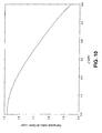
- FIG. 10 is a graph plotting refractive index as a function of outer layer radius.
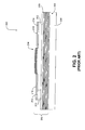
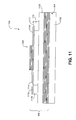
- FIG. 11 is a schematic of a laser that incorporates the optical cavity shown in FIG. 9.
- FIG. 12 is a schematic of a filter that incorporates the optical cavity shown in FIG. 9.
- FIG. 3 provides a schematic representation of a prior art optical cavity 300 that incorporates a concave, semispherical mirror 302.
- the mirror 302 is centered about an axis of symmetry 304 and faces a planar mirror 306 at the other end of the cavity 300.
- the concave, semispherical mirror 302 has a radius of curvature, ⁇ . Distances outward from the axis of symmetry 304 to points on the surface of the concave, semispherical mirror 302 are represented by the distance, ⁇ .
- the arrangement shown in FIG. 3 provides a focusing effect such that a beam of light 308 can travel back and forth between the mirrors 302, 306 without a significant portion of the light being lost through diffraction.
- the provision of a concave, semispherical mirror 302 counteracts the natural tendency for a light beam to continuously expand as it travels.
- the optical cavity 300, the focusing power of the mirror 302, the separation of the mirrors 302 and 306, and the beam diameter can each be selected so that little light leaks out past the edges of the mirrors as the light travels back and forth within the cavity 300.
- FIG. 4 illustrates one such alternative.
- an optical cavity 400 can be constructed with first and second planar mirrors 402 and 404.
- a lens 408 e.g., a ground and polished glass lens
- the lens 408 comprises a relatively flat, positive lens capable of focusing light back on itself.
- the lens 408 must be produced with very high precision and would need to be supported within the cavity 400 in a very precise manner. Such precision requires fabrication and mechanical complexity that could render the design impractical for repeatable production.
- the lens 408 would most likely need an antireflection coating on both its top and bottom surfaces to reduce undesired reflections. Inclusion of such antireflection coatings would degrade the performance of the optical cavity 400 by increasing the length of the cavity. As is known in the art, the best performance is normally achieved when the length of the optical cavity is kept very small, for instance, on the order of several light wavelengths. Accordingly, it would be desirable to obtain the focusing effect provided by a lens without actually using a lens within the optical cavity.
- FIG. 5 illustrates a first optical cavity 500 of the invention.
- the optical cavity 500 includes a first reflector 502 and a second reflector 504 that are positioned at opposite ends of the cavity.
- Each of the reflectors 502, 504 is normally constructed as a distributed Bragg reflector (DBR) comprising a plurality of semi-conductor and/or dielectric layers 506 in a stacked configuration.
- DBR distributed Bragg reflector
- the reflectors 502, 504 could alternatively be constructed of known metal materials, semiconductor and/or dielectric materials are preferred in that reflectors can be made with greater precision when constructed of these materials, especially where the scale of the reflectors is very small.
- each reflector 502, 504 comprises alternating semiconductor or dielectric materials having different indices of refraction.
- each layer 506 has a wave thickness equal to ⁇ / 4n (i.e., quarter wave optical thickness) where ⁇ is the wavelength of the light and n is the refractive index of the material.
- the semiconductor or dielectric layers 506 can also alternate between relatively thick layers 510 and relatively thin layers 512.
- the relatively thick layers 510 can comprise silicon dioxide (SiO 2 ) and the relatively thin layers can comprise titanium dioxide (TiO 2 ).
- the layers 506 are shown and described herein as being relatively thick and thin, each normally is near quarter wave optical thickness due to their differences in index of refraction. Although a specific number of layers 506 is shown for each of the reflectors 502, 504 it is to be understood that alternative configurations are feasible.
- the first reflector 502 includes a convex outer layer 514 that comprises a convex, semispherical surface 516. Accordingly, the first reflector 502 can be designated a convex reflector.
- the convex, semispherical shape of the surface 516 provides a focusing effect similar to that of the lens 408 shown in FIG. 4 and to that of the concave, semispherical mirror 302 shown in FIG. 3.
- the convex, semispherical shape introduces a reflection delay that is radially symmetric from the center of the reflector 502. This delay creates a focusing effect that reflects light 518 back on itself to reduce diffraction losses.
- the convex outer layer 514 can be constructed with a particular thickness, t , that varies as a function of a distance, ⁇ , from the axis of symmetry 520 of the first reflector 502.
- This thickness can be determined through normal experimentation by persons having ordinary skill in the art. Alternatively, this thickness can be estimated by analogy to existing optical cavities that use concave, semispherical mirrors.
- One concave arrangement that has been shown to be effective is that proposed by Vakhshoori, et al. in an article entitled “Microelectromechanical Tunable Filter with Stable Path Symmetric Cavity," which appeared in Electronics Letters on May 27, 1999. In this article, Vakhshoori, et al.
- VCSEL vertical cavity surface emitting laser
- the thickness, t , of the convex outer layer 514 can be chosen to emulate a concave, semispherical mirror such as that of the Vakhshoori, et al. VCSEL.
- the thickness, t , of the layer 514 can be selected to provide a phase delay, ⁇ , representative of the delay in phase between two light rays L 0 and L 1 reflected off of the first reflector 502 and separated by a distance, ⁇ (see FIG. 5) that is equal to the phase delay, ⁇ , between two light rays L 0 and L 1 reflected off of the first mirror 302 and separated by the same distance, ⁇ (see FIG. 3).
- the phase delay, ⁇ , at this distance is equal to -0.16 ⁇ .
- the thickness, t of the convex outer layer 514 can be constructed to emulate this phase delay, ⁇ , to obtain the same focusing effect of the concave arrangement of FIG. 3. This can be accomplished by first calculating the phase, ⁇ , of a light ray that travels parallel to the axis of symmetry 520 through a given thickness, t , of semiconductor or dielectric material. Although light is reflected multiple times at each layer interface 508, the details for the planar layers 506 of the first reflector 502 need not be considered if it is assumed that the stack comprising these layers is thick enough to reflect nearly all the light.
- R planar stack
- 2 1
- R planar stack is the optical power reflectivity of the light beam
- r planar stack is the optical field reflectivity of the light beam.
- the phase of r comp is that of the composite reflector 502 comprising the convex outer layer 514 and the planar layers 506.
- phase of the reflected light at the reference plane 522 is added to the phase of r comp to account for the difference between the phase at the convex, semispherical surface 516 and at the reference plane 522.
- the quantity t(2n / ⁇ ) is used to permit reference to a single graph irrespective of refractive index, n, and wavelength, ⁇ .
- the graph can be used to relate phase delay, ⁇ , to the thickness, t , of the convex outer layer 514.
- this phase delay pertains to a thickness value ( i.e ., t(2n / ⁇ ) ) of 0.14.
- the thickness, t , of the outer layer 514 can be determined in this manner for any distance, ⁇ , through relation of the phase delay, ⁇ , with thickness. It is to be noted that FIG. 6 is quantitative in nature and was generated assuming a variable thickness outer layer 514 that terminated a quarter wave layered stack. Persons having ordinary skill will appreciate that the thickness, t , of the convex outer layer 514 can alternatively be derived as a function of the distance, ⁇ , through conventional mathematics.
- FIG. 7 illustrates an example laser 700 incorporating the optical cavity 500 shown in FIG. 5.
- This laser is shown and described herein to provide an example application of the inventive optical cavity 500. Therefore, it is to be understood that the laser could have alternative construction, if desired.
- the laser 700 includes a substrate 702.
- the substrate 702 can comprise an n-type doped semiconductor material.
- the substrate 702 is adapted to receive light from a separate light source (not shown).
- an active region 706 Disposed within the optical cavity 500 is an active region 706 where electrons and holes are recombined to produce laser light.
- This region 706 can include a plurality of quantum wells (not shown).
- the active region 706 can comprise an intrinsic (i.e., undoped or lightly doped) semiconductor layer.
- support posts 710 are used to suspend the first reflector 502 above the active region 706.
- posts 710 are shown, it will be understood that alternative support means could be provided, if desired.
- the support posts 710 can be formed of a dielectric material such as a polymeric material.
- Mounted on the support posts 710 are support tethers 712 that directly support the first reflector 502.
- tuning electrodes 714 are used to deliver voltage to the first reflector 502.
- the first reflector 502 is displaced downwardly toward the second reflector 504 to adjust ( i.e., reduce) the length of the optical cavity 500 to change the frequency of emission of the laser 700.
- light is delivered to the laser 700, for example, through the substrate 702.
- This light reflects back and forth off of the first and second reflectors 502 and 504 until its intensity increases to the point at which light is transmitted through one of the reflectors, normally the first reflector 502.
- voltage can be provided to the first reflector 502 to cause it to be displaced in the manner described above.
- FIG. 8 illustrates an example filter 800 that incorporates the optical cavity 500 shown in FIG. 5.
- this filter 800 is shown and described as an example application of the optical cavity 500. Therefore, it is to be appreciated that alternative constructions are feasible.
- the filter 800 is similar in design to the laser 700. Accordingly, the filter 800 can include a substrate 802, a first tuning electrode 804, support posts 806, support tethers 808, and second tuning electrodes 810. In that the filter 800 is used to filter light as opposed to generate light, the filter 800 does not include a gain medium such as active region 706.
- the filter 800 In use, light is provided to the filter 800 through either its top or bottom such that the light reaches the optical cavity 500. Within the cavity 500, the light travels back and forth between the reflectors 502, 504 and ultimately is transmitted through one of the reflectors 502, 504 (the reflector opposite to that through which the light entered the filter 800) at a desired optical frequency.
- the frequency of light that is emitted from the filter 800 is controlled by adjusting the displacement of the first reflector 502 by provided an appropriate voltage to the reflector with the tuning electrodes 804, 810.
- FIG. 9 illustrates a second optical cavity 900 of the invention.
- This optical cavity 900 is similar in many ways to the first optical cavity 500 shown in FIG. 5.
- the optical cavity 900 includes a first reflector 902 and a second reflector 904 that are positioned at opposite ends of the cavity.
- each of the reflectors 902, 904 is normally constructed as a DBR comprising a plurality of semi-conductor and/or dielectric layers 906 having quarter wave optical thicknesses and different indices of refraction.
- the reflector layers 906 of the second optical cavity 900 can alternate between relatively thick layers 908 and relatively thin layers 910.
- the relatively thick layers 908 can comprise silicon carbide (SiCx) or SiO 2 and the thin layers can comprise TiO 2 .
- the first reflector 902 of the second optical cavity 900 comprises a planar outer layer 912 having an index of refraction that varies radially outward from the central axis 914 of the reflector. More particularly, the index of refraction of the outer layer 912 is largest at its axial center and decreases outwardly therefrom.
- this varied index of refraction provides a focusing effect on light 916 reflected back and forth between the reflectors 902, 904.
- This focusing effect occurs because, due to the difference in index of refraction, the optical distance traveled through the outer layer 912 by a light ray along the axis of symmetry 914 is longer than that traveled by a parallel light ray separated a distance, ⁇ , from this axis.
- the planar outer layer 912 is constructed to have a refractive index, n, that varies as a function of the distance, ⁇ , from the axis of symmetry 914.
- This refractive index can be determined through normal experimentation by persons having ordinary skill in the art.
- this refractive index can be estimated in similar manner to that described above with regard to the first optical cavity 500 by analogy to an optical cavity having a concave, semispherical mirror.
- the refractive index, n , of the outer layer 912 can be chosen to emulate a convex, semispherical mirror having a radius of curvature, ⁇ , of 300 ⁇ m (see FIG. 3).
- the focusing effect can be quantified by evaluating the optical phase, ⁇ , along paths parallel to the axis of symmetry 914.
- k (2 ⁇ n )/ ⁇ , where n is the local index of refraction of the material and ⁇ is the free space wavelength of light.
- the field reflectivity, r is given by r l +exp[- i 2 k . l ] 1+r l exp[- i 2 k .
- Equation 11 the index of refraction, n, at each value of ⁇ can be determined from Equations 8-10.
- FIG. 10 is a refractive index profile for the outer layer 912.
- the composition of the outer layer 912 can likewise be varied as a function of radius.
- the composition can be varied to primarily comprise SiC x at the center of the outer layer 912 and SiO 2 adjacent the edges of the layer.
- SiC x has a refractive index of approximately 2.5, while SiO 2 has a refractive index of approximately 1.5.
- a layer of SiC x can first be formed through conventional material deposition techniques. Once the layer is formed, its composition can be modified through a selective oxidation process, e.g., using oxygen (excited to a plasma or ionic form) to transform portions of the SiC x into SiO 2 .
- a selective mask structure can be used, for instance, a structure having a larger amount of mask material in the center of the composition layer that decreases radially therefrom.
- FIG. 11 illustrates an example laser 1100 incorporating the optical cavity 900 shown in FIG. 9.
- the laser 1100 includes a substrate 1102 that can comprise an n-type doped semiconductor material.
- an active region 1106 Disposed within the optical cavity 900 is an active region 1106 that can comprise an intrinsic (i.e., undoped or lightly doped) semiconductor layer.
- the laser 1100 includes support posts 1110 and support tethers that are used to suspend the first reflector 902 above the active region 1106. Although posts 1110 and tethers are shown, it will be understood that alternative support means could be provided, if desired.
- tuning electrodes 1114 are used to deliver voltage to the first reflector 902 and displace it downwardly toward the second reflector 904 to adjust ( i.e. , reduce) the length of the optical cavity 900.
- FIG. 12 illustrates an example filter 1200 that incorporates the optical cavity 900 shown in FIG. 9.
- the filter 1200 is shown and described as an example application of the optical cavity 900. Therefore, it is to be appreciated that alternative constructions are feasible.
- the filter 1200 can include a substrate 1202, a first tuning electrode 1204, support posts 1206, support tethers 1208, and second tuning electrodes 1210. In that the filter 1200 is used to filter light as opposed to generate light, the filter 1200 does not include a gain medium such as active region 1106.
Applications Claiming Priority (2)
| Application Number | Priority Date | Filing Date | Title |
|---|---|---|---|
| US778661 | 2001-02-06 | ||
| US09/778,661 US6833958B2 (en) | 2001-02-06 | 2001-02-06 | Optical cavities for optical devices |
Publications (3)
| Publication Number | Publication Date |
|---|---|
| EP1229374A2 true EP1229374A2 (fr) | 2002-08-07 |
| EP1229374A3 EP1229374A3 (fr) | 2003-04-02 |
| EP1229374B1 EP1229374B1 (fr) | 2006-03-15 |
Family
ID=25114052
Family Applications (1)
| Application Number | Title | Priority Date | Filing Date |
|---|---|---|---|
| EP01125548A Expired - Lifetime EP1229374B1 (fr) | 2001-02-06 | 2001-10-25 | Résonateurs optiques pour dispositifs optiques |
Country Status (4)
| Country | Link |
|---|---|
| US (1) | US6833958B2 (fr) |
| EP (1) | EP1229374B1 (fr) |
| JP (1) | JP2002319740A (fr) |
| DE (1) | DE60117906T2 (fr) |
Families Citing this family (10)
| Publication number | Priority date | Publication date | Assignee | Title |
|---|---|---|---|---|
| US7370185B2 (en) * | 2003-04-30 | 2008-05-06 | Hewlett-Packard Development Company, L.P. | Self-packaged optical interference display device having anti-stiction bumps, integral micro-lens, and reflection-absorbing layers |
| JP4439199B2 (ja) * | 2003-03-20 | 2010-03-24 | 株式会社リコー | 垂直共振器型面発光半導体レーザ装置、およびそれを用いた光論理演算装置、波長変換装置、光パルス波形整形装置、ならびに光伝送システム |
| US7447891B2 (en) * | 2003-04-30 | 2008-11-04 | Hewlett-Packard Development Company, L.P. | Light modulator with concentric control-electrode structure |
| JP2006269664A (ja) * | 2005-03-23 | 2006-10-05 | Fuji Xerox Co Ltd | 発光デバイス、光通信システム、および発光デバイスの製造方法 |
| KR20070060209A (ko) * | 2005-12-08 | 2007-06-13 | 삼성전자주식회사 | 수직 외부 공동 면발광 레이저 |
| JP5105626B2 (ja) * | 2009-10-09 | 2012-12-26 | 株式会社リコー | 面発光レーザ素子およびその作製方法および面発光レーザアレイおよび波長多重伝送システム |
| JP2015233127A (ja) | 2014-05-12 | 2015-12-24 | キヤノン株式会社 | 面発光レーザ、レーザアレイ、光源装置、情報取得装置及び光干渉断層計 |
| JP6685701B2 (ja) * | 2014-12-26 | 2020-04-22 | キヤノン株式会社 | 面発光レーザ、情報取得装置、撮像装置、レーザアレイ及び面発光レーザの製造方法 |
| JP6576092B2 (ja) | 2015-04-30 | 2019-09-18 | キヤノン株式会社 | 面発光レーザ、情報取得装置及び撮像装置 |
| JP2016054314A (ja) * | 2015-12-01 | 2016-04-14 | ヒューレット−パッカード デベロップメント カンパニー エル.ピー.Hewlett‐Packard Development Company, L.P. | マルチモードのモノリシック垂直共振器面発光レーザアレイ及びこれを含むレーザシステム |
Citations (2)
| Publication number | Priority date | Publication date | Assignee | Title |
|---|---|---|---|---|
| WO1999050940A1 (fr) * | 1998-03-30 | 1999-10-07 | Bandwidth 9 | Cavites optiques verticales produites avec epitaxie de zone selective |
| WO1999052647A1 (fr) * | 1998-04-16 | 1999-10-21 | The University Of New Mexico | Microstructures optiques non planaires |
Family Cites Families (12)
| Publication number | Priority date | Publication date | Assignee | Title |
|---|---|---|---|---|
| US4815084A (en) * | 1987-05-20 | 1989-03-21 | Spectra Diode Laboratories, Inc. | Semiconductor laser with integrated optical elements |
| US5151917A (en) * | 1991-04-18 | 1992-09-29 | Coherent, Inc. | Laser resonators employing diffractive optical elements |
| JPH05145148A (ja) * | 1991-11-25 | 1993-06-11 | Sony Corp | 固体レーザ共振器 |
| US5291502A (en) * | 1992-09-04 | 1994-03-01 | The Board Of Trustees Of The Leland Stanford, Jr. University | Electrostatically tunable optical device and optical interconnect for processors |
| US5428634A (en) * | 1992-11-05 | 1995-06-27 | The United States Of America As Represented By The United States Department Of Energy | Visible light emitting vertical cavity surface emitting lasers |
| US5633527A (en) * | 1995-02-06 | 1997-05-27 | Sandia Corporation | Unitary lens semiconductor device |
| US5583683A (en) * | 1995-06-15 | 1996-12-10 | Optical Corporation Of America | Optical multiplexing device |
| US5739945A (en) * | 1995-09-29 | 1998-04-14 | Tayebati; Parviz | Electrically tunable optical filter utilizing a deformable multi-layer mirror |
| US5629951A (en) * | 1995-10-13 | 1997-05-13 | Chang-Hasnain; Constance J. | Electrostatically-controlled cantilever apparatus for continuous tuning of the resonance wavelength of a fabry-perot cavity |
| US5666225A (en) * | 1996-02-26 | 1997-09-09 | Jds Fitel Inc. | Multi-pass etalon filter |
| US6438149B1 (en) * | 1998-06-26 | 2002-08-20 | Coretek, Inc. | Microelectromechanically tunable, confocal, vertical cavity surface emitting laser and fabry-perot filter |
| JP2002500446A (ja) | 1997-12-29 | 2002-01-08 | コアテック・インコーポレーテッド | マイクロエレクトロメカニカル的に同調可能な共焦型の垂直キャビティ表面放出レーザ及びファブリー・ペローフィルタ |
-
2001
- 2001-02-06 US US09/778,661 patent/US6833958B2/en not_active Expired - Fee Related
- 2001-10-25 EP EP01125548A patent/EP1229374B1/fr not_active Expired - Lifetime
- 2001-10-25 DE DE60117906T patent/DE60117906T2/de not_active Expired - Lifetime
-
2002
- 2002-02-06 JP JP2002029366A patent/JP2002319740A/ja active Pending
Patent Citations (2)
| Publication number | Priority date | Publication date | Assignee | Title |
|---|---|---|---|---|
| WO1999050940A1 (fr) * | 1998-03-30 | 1999-10-07 | Bandwidth 9 | Cavites optiques verticales produites avec epitaxie de zone selective |
| WO1999052647A1 (fr) * | 1998-04-16 | 1999-10-21 | The University Of New Mexico | Microstructures optiques non planaires |
Non-Patent Citations (2)
| Title |
|---|
| KOCH B J ET AL: "SINGLE-MODE VERTICAL CAVITY SURFACE EMITTING LASER BY GRADED-INDEX LENS SPATIAL FILTERING" APPLIED PHYSICS LETTERS, AMERICAN INSTITUTE OF PHYSICS. NEW YORK, US, vol. 70, no. 18, 5 May 1997 (1997-05-05), pages 2359-2361, XP000701336 ISSN: 0003-6951 * |
| LEGER J R ET AL: "MICRO-OPTICS IN VCSEL AND SOLID-STATE LASER RESONATORS" PROCEEDINGS OF THE SPIE, SPIE, BELLINGHAM, VA, US, vol. 3267, 1998, pages 107-115, XP008012899 * |
Also Published As
| Publication number | Publication date |
|---|---|
| US20020135909A1 (en) | 2002-09-26 |
| US6833958B2 (en) | 2004-12-21 |
| DE60117906D1 (de) | 2006-05-11 |
| JP2002319740A (ja) | 2002-10-31 |
| EP1229374A3 (fr) | 2003-04-02 |
| EP1229374B1 (fr) | 2006-03-15 |
| DE60117906T2 (de) | 2006-12-14 |
Similar Documents
| Publication | Publication Date | Title |
|---|---|---|
| US6661830B1 (en) | Tunable optically-pumped semiconductor laser including a polarizing resonator mirror | |
| Baillard et al. | Interference-filter-stabilized external-cavity diode lasers | |
| EP2636111B1 (fr) | Elément optique pour laser à émission de surface à cavité externe verticale | |
| US7327772B2 (en) | Optical resonator with mirror structure suppressing higher order transverse modes | |
| KR101463704B1 (ko) | 면 발광 레이저, 면 발광 레이저 어레이, 및 화상 형성 장치 | |
| JP2003504880A (ja) | 垂直空洞表面発光性レーザーの偏光制御 | |
| JPH07170016A (ja) | 同調可能な外部空洞型レーザの出力特性を最適化するための方法と装置 | |
| EP1229374A2 (fr) | Résonateurs optiques pour dispositifs optiques | |
| JP2012009727A (ja) | 面発光型半導体レーザ、面発光型半導体レーザ装置、光伝送装置および情報処理装置 | |
| US20230378720A1 (en) | Vertical laser emitter and manufacturing method thereof | |
| GB2582378A (en) | Vertical external cavity surface emitting laser with improved external mirror structure | |
| US20200412093A1 (en) | External-cavity quantum cascade laser | |
| US9929538B2 (en) | Surface emitting laser and image forming apparatus | |
| JP2014500622A (ja) | 偏光安定性面発光レーザーダイオード | |
| JP5743520B2 (ja) | 面発光レーザ及び画像形成装置 | |
| WO2001095445A2 (fr) | Laser a semi-conducteurs a pompage optique dont la sortie est couplee a une fibre optique | |
| GB2585069A (en) | Vertical Surface Emitting Laser with Improved Polarization Stability | |
| US20070058688A1 (en) | End pumping vertical external cavity surface emitting laser | |
| KR20190041318A (ko) | 가변 레이저 소자 | |
| US6768757B2 (en) | Cavity mirror for optically-pumped vertical-cavity surface-emitting laser (VCSEL) | |
| CN111837301B (zh) | 包括至少一个vcsel和扩散透镜的发光器件 | |
| Büttner et al. | Folded diffractive laser resonators with user-defined fundamental mode |
Legal Events
| Date | Code | Title | Description |
|---|---|---|---|
| PUAI | Public reference made under article 153(3) epc to a published international application that has entered the european phase |
Free format text: ORIGINAL CODE: 0009012 |
|
| AK | Designated contracting states |
Kind code of ref document: A2 Designated state(s): AT BE CH CY DE DK ES FI FR GB GR IE IT LI LU MC NL PT SE TR |
|
| AX | Request for extension of the european patent |
Free format text: AL;LT;LV;MK;RO;SI |
|
| PUAL | Search report despatched |
Free format text: ORIGINAL CODE: 0009013 |
|
| AK | Designated contracting states |
Kind code of ref document: A3 Designated state(s): AT BE CH CY DE DK ES FI FR GB GR IE IT LI LU MC NL PT SE TR |
|
| AX | Request for extension of the european patent |
Extension state: AL LT LV MK RO SI |
|
| 17P | Request for examination filed |
Effective date: 20030829 |
|
| AKX | Designation fees paid |
Designated state(s): DE FR GB |
|
| 17Q | First examination report despatched |
Effective date: 20040122 |
|
| GRAP | Despatch of communication of intention to grant a patent |
Free format text: ORIGINAL CODE: EPIDOSNIGR1 |
|
| GRAS | Grant fee paid |
Free format text: ORIGINAL CODE: EPIDOSNIGR3 |
|
| GRAA | (expected) grant |
Free format text: ORIGINAL CODE: 0009210 |
|
| AK | Designated contracting states |
Kind code of ref document: B1 Designated state(s): DE FR GB |
|
| REG | Reference to a national code |
Ref country code: GB Ref legal event code: FG4D |
|
| REF | Corresponds to: |
Ref document number: 60117906 Country of ref document: DE Date of ref document: 20060511 Kind code of ref document: P |
|
| REG | Reference to a national code |
Ref country code: GB Ref legal event code: 732E |
|
| ET | Fr: translation filed | ||
| RAP2 | Party data changed (patent owner data changed or rights of a patent transferred) |
Owner name: AVAGO TECHNOLOGIES FIBER IP (SINGAPORE) PTE. LTD. |
|
| PLBE | No opposition filed within time limit |
Free format text: ORIGINAL CODE: 0009261 |
|
| STAA | Information on the status of an ep patent application or granted ep patent |
Free format text: STATUS: NO OPPOSITION FILED WITHIN TIME LIMIT |
|
| 26N | No opposition filed |
Effective date: 20061218 |
|
| REG | Reference to a national code |
Ref country code: FR Ref legal event code: ST Effective date: 20080630 |
|
| PGFP | Annual fee paid to national office [announced via postgrant information from national office to epo] |
Ref country code: FR Payment date: 20061017 Year of fee payment: 6 |
|
| PG25 | Lapsed in a contracting state [announced via postgrant information from national office to epo] |
Ref country code: FR Free format text: LAPSE BECAUSE OF NON-PAYMENT OF DUE FEES Effective date: 20071031 |
|
| PGFP | Annual fee paid to national office [announced via postgrant information from national office to epo] |
Ref country code: DE Payment date: 20101020 Year of fee payment: 10 |
|
| PGFP | Annual fee paid to national office [announced via postgrant information from national office to epo] |
Ref country code: GB Payment date: 20101020 Year of fee payment: 10 |
|
| PG25 | Lapsed in a contracting state [announced via postgrant information from national office to epo] |
Ref country code: DE Free format text: LAPSE BECAUSE OF NON-PAYMENT OF DUE FEES Effective date: 20120501 |
|
| REG | Reference to a national code |
Ref country code: DE Ref legal event code: R119 Ref document number: 60117906 Country of ref document: DE Effective date: 20120501 |
|
| GBPC | Gb: european patent ceased through non-payment of renewal fee |
Effective date: 20121025 |
|
| PG25 | Lapsed in a contracting state [announced via postgrant information from national office to epo] |
Ref country code: GB Free format text: LAPSE BECAUSE OF NON-PAYMENT OF DUE FEES Effective date: 20121025 |