EP1231671A2 - Internal antenna for mobile communications device - Google Patents
Internal antenna for mobile communications device Download PDFInfo
- Publication number
- EP1231671A2 EP1231671A2 EP02250850A EP02250850A EP1231671A2 EP 1231671 A2 EP1231671 A2 EP 1231671A2 EP 02250850 A EP02250850 A EP 02250850A EP 02250850 A EP02250850 A EP 02250850A EP 1231671 A2 EP1231671 A2 EP 1231671A2
- Authority
- EP
- European Patent Office
- Prior art keywords
- antenna
- balanced
- ground plane
- antenna elements
- elements
- Prior art date
- Legal status (The legal status is an assumption and is not a legal conclusion. Google has not performed a legal analysis and makes no representation as to the accuracy of the status listed.)
- Granted
Links
Images


Classifications
-
- H—ELECTRICITY
- H01—ELECTRIC ELEMENTS
- H01Q—ANTENNAS, i.e. RADIO AERIALS
- H01Q1/00—Details of, or arrangements associated with, antennas
- H01Q1/12—Supports; Mounting means
- H01Q1/22—Supports; Mounting means by structural association with other equipment or articles
- H01Q1/24—Supports; Mounting means by structural association with other equipment or articles with receiving set
- H01Q1/241—Supports; Mounting means by structural association with other equipment or articles with receiving set used in mobile communications, e.g. GSM
- H01Q1/242—Supports; Mounting means by structural association with other equipment or articles with receiving set used in mobile communications, e.g. GSM specially adapted for hand-held use
- H01Q1/243—Supports; Mounting means by structural association with other equipment or articles with receiving set used in mobile communications, e.g. GSM specially adapted for hand-held use with built-in antennas
-
- H—ELECTRICITY
- H01—ELECTRIC ELEMENTS
- H01Q—ANTENNAS, i.e. RADIO AERIALS
- H01Q9/00—Electrically-short antennas having dimensions not more than twice the operating wavelength and consisting of conductive active radiating elements
- H01Q9/04—Resonant antennas
- H01Q9/30—Resonant antennas with feed to end of elongated active element, e.g. unipole
- H01Q9/42—Resonant antennas with feed to end of elongated active element, e.g. unipole with folded element, the folded parts being spaced apart a small fraction of the operating wavelength
Definitions
- This invention relates to an internal antenna for a mobile communications device such as a mobile telephone.
- rf stage of a mobile communications device It is common for the rf stage of a mobile communications device to include a balanced power amplifier stage.
- the main advantages of balanced power amplifiers include lower distortion and better rejection of power supply noise.
- Power amplifiers designed for mobile communications equipment typically have an output impedance of around 5 ohms, requiring an impedance matching network to connect to a conventional antenna which is generally designed to have a 50 ohm impedance.
- a balanced antenna for connecting to a balanced power amplifier stage in a portable communications device, the balanced power amplifier stage having first and second outputs, the antenna comprising a ground plane and first and second antenna elements spaced apart from each other and from the ground plane, wherein the antenna elements are arranged to be opposite one another and each of the antenna elements has a feed point connectable to one of the outputs from the power amplifier stage.
- the balanced antenna according to the invention can interface directly to a balanced power amplifier (PA) stage without the need for a lossy conversion network.
- PA power amplifier
- the printed circuit board (PCB) of the mobile communications device is not part of the antenna.
- the PCB is part of the antenna and a large portion of the radiated rf signal is emitted from the telephone's PCB. Therefore, for a balanced antenna, the antenna induced currents in the ground plane of the PCB are much smaller and less likely to cause disturbances in the telephone's electronics.
- the antenna according to the invention can be tuned to impedances between about 3 to 15 ohms, so that the balanced PA stage, which typically has an output impedance of around 5 ohms, can be connected directly to the antenna without an impedance matching network.
- the elements can be substantially identical and one element can be reversed with respect to the other.
- the balanced antenna can include a floating ground between the ground plane and the antenna elements.
- the floating ground avoids the problem of a component mounted on the printed circuit board (PCB) under the antenna affecting the impedance to ground of the radiating element of the antenna closest to the component. It also avoids disturbance of the operation of the component by the antenna field and so can make it possible to utilise the PCB area under the antenna.
- PCB printed circuit board
- a portable communications device comprising a circuit board having a plurality of electronic components mounted thereon and a balanced antenna, the balanced antenna comprising first and second substantially parallel antenna elements mounted to the board, each of the antenna elements having a top edge and a bottom edge, the bottom edge being nearer the board than the top edge, the device further comprising a ground plane disposed between the bottom edge of the antenna elements and the board, the ground plane being electrically isolated from the antenna elements and the board.
- the invention provides a balanced antenna for a portable communications device, comprising a ground plane and first and second substantially similar antenna elements spaced from the ground plane, the first and second elements being substantially parallel to the ground plane and being aligned in opposite directions with respect to one another.
- a method of manufacturing a balanced antenna for connecting to a balanced power amplifier stage in a portable communications device the balanced power amplifier stage having first and second outputs, the antenna comprising a ground plane and first and second antenna elements spaced apart from each other and from the ground plane, wherein the antenna elements are arranged to be opposite one another and to overlap to a predetermined extent, and each of the antenna elements has a feed point connectable to one of the outputs from the power amplifier stage, the method comprising varying the extent to which the antenna elements overlap to tune the antenna for use in a predetermined frequency band.
- a mobile station in the form of a mobile telephone handset 1 includes a microphone 2, keypad 3, with soft keys 4 which can be programmed to perform different functions, an LCD display 5, a speaker 6 and an antenna 7 which is contained within the housing.
- the location of the antenna 7 is illustrated in Figure 2, which shows the back of the handset 1 with a rear cover 8 removed.
- the mobile station 1 is operable to communicate through cellular radio links with individual public land mobile networks (PLMNs), shown schematically as PLMN A and PLMN B.
- PLMNs A and B may utilise different frequency bands.
- PLMN A is a GSM 1800 MHz network
- PLMN B is a GSM 900 MHz network.
- the handset communicates over a cellular radio link with its home network PLMN A (shown as HPLMN) in a first configuration i.e. using a frequency band appropriate to PLMN A.
- PLMN A home network
- PLMN B home network
- one of the keys on the handset for example, one of the soft keys 4
- PLMN B may be operated to select a second operational configuration i.e. a frequency band associated with PLMN B.
- Figure 3 illustrates the major circuit components of the telephone handset 1. Signal processing is carried out under the control of a digital micro-controller 9 which has an associated flash memory 10. Electrical analogue audio signals are produced by microphone 2 and amplified by pre-amplifier 11. Similarly, analogue audio signals are fed to the speaker 6 through an amplifier 12.
- the micro-controller 9 receives instruction signals from the keypad and soft keys 3, 4 and controls operation of the LCD display 5.
- a smart card 13 in the form of a GSM SIM card which contains the usual GSM international mobile subscriber identity (IMSI) and an encryption key K i that is used for encoding the radio transmission in a manner well known per se.
- IMSI GSM international mobile subscriber identity
- K i an encryption key that is used for encoding the radio transmission in a manner well known per se.
- the SIM card is removably received in a SIM card reader 14.
- the mobile telephone circuitry includes a codec 15 and an rf stage 16 including a balanced power amplifier stage 17 feeding the antenna 7.
- the codec 15 receives analogue signals from the microphone amplifier 11, digitises them into a GSM signal format and feeds them to the rf stage 16 for transmission through the antenna 7 to the PLMN shown in Figure 1.
- signals received from the PLMN are fed through the antenna 7 to be demodulated in the rf stage 16 and fed to codec 15, so as to produce analogue signals fed to the amplifier 12 and speaker 6.
- an antenna 7 comprises a first planar conductive plate 20 spaced apart from and generally parallel to a second planar conductive plate 21.
- Each of the first and second conductive plates 20, 21 forms a rectangular patch antenna element 18mm long and 3mm wide.
- a conductive leg 22 extends from a bottom corner of each conductive plate 20, 21, the leg 22 resting on a non-conductive pad 23 on a third conductive plate 24 forming a ground plane, the first and second plates 20, 21 being substantially perpendicular to the third plate 24.
- the third conductive plate 24 is for example the printed circuit board (PCB) to the underside of which the handset components are mounted.
- PCB printed circuit board
- the antenna could be constructed by using a "two-shot moulding" (MID) technique which enable the antenna elements to be fixed in the proper positions.
- MID two-shot moulding
- the MID technique provides for air between the elements and plastic on their reverse sides to fix the antenna elements. Air between the elements, where the electrical field is at a maximum, minimises the electrical loss in the antenna.
- the antenna can also be made having mouldable plastic between the antenna elements and air at the reverse sides. In this case low loss plastic materials are preferably used.
- the antenna 7 is tuned by changing the relative position of the two slot elements 20, 21, which changes the capacitive coupling between the elements.
- the inductive coupling between the elements is also controlled by displacement of the elements, as shown in Figure 5.
- Figure 4 shows one extreme of relative position in which the elements overlap completely. This arrangement is close to that of a slot antenna. The other extreme of position (not shown) is obtained by moving the legs 22 of each of the patch elements close together so that the elements extend in opposite directions and do not overlap to any substantial extent. This arrangement is effectively a dipole antenna.
- Figure 5 shows a dipole-like antenna structure where the overall arrangement is similar to Figure 4 but in which the geometry of the plates and support structure is slightly different, so that the antenna elements 20, 21 do not overlap at all.
- the slot antenna elements 20, 21 are substantially rectangular elements 10mm long by 3mm wide, with an arm 26 1mm wide extending from one side of each of the elements to meet the supporting leg 22 at right angles.
- Figure 6 shows the Smith chart for the first arrangement described above in relation to Figure 4, while Figure 7 illustrates the frequency response of the arrangement, showing a resonant frequency at 0.9GHz, so that the antenna is suitable for use at the GSM 900MHz band.
- the bandwidth of the antenna is approximately 12 % having a return loss (S11) less than -8 dB.
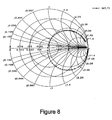
- Figure 8 shows the Smith chart for the second arrangement described above in relation to Figure 5, while Figure 9 illustrates the frequency response of the arrangement, showing a resonant frequency at 1.85GHz, so that the antenna is suitable for use at the GSM 1800MHz and 1900MHz bands.
- FIG 10 shows a balanced antenna as described above in relation to Figure 4, with the addition of a floating ground 27.
- the floating ground 27 is an area of conductive material made of same material as the balanced antenna.
- the floating ground 27 is disposed between the antenna elements 20,21 and the PCB 24, for example 1 mm from the bottom of the antenna elements 20, 21 and 2 mm from the PCB 24.
- the length of the floating ground is made approximately 2 mm shorter than the antenna elements 20,21.
- the floating ground 27 is supported on an area of dielectric-like plastic 28 which is used in the MID technique and has no electrical connections to the ground plane 24 or the antenna plates 20, 21. Since the fields emitted from the two parts 20, 21 of the balanced antenna are identical in magnitude and opposite in phase, the floating ground has the properties of an electrical ground.
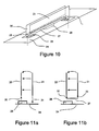
- Figure 11a shows the electric field generated when the antenna is in use between the first and second antenna elements 20, 21, the PCB 24 and a component 29 mounted to the PCB 24.
- the electric field 30 between the first antenna element 20 and the PCB 24 is altered by the presence of the component 29, by comparison with the field 31 between the second antenna plate 21 and the PCB 24.
- the effect of the position of the first element 20 of the balanced antenna 7 over the component 29 is to lower the impedance to ground for the first antenna element 20, which can significantly alter antenna behaviour.
- Figure 11b illustrates the effect of introducing a floating ground 27.
- the electric fields 32, 33 between each of the antenna elements 20, 21 and the floating ground 27 are unaffected by the presence of the component 29 on the PCB.
- the use of a floating ground 27 therefore makes the PCB area under the antenna 7 available for mounting electrical components. The components will not affect antenna operation and their operation will in turn be unaffected by the antenna field.
- Figures 12 and 13 show a further embodiment of a balanced antenna.
- the antenna comprises first and second substantially identical conductive elements 35, 36 disposed on either side of a 1mm thick dielectric layer 37, comprising a material with a high dielectric constant, for example greater than 8, such as ceramics materials.
- the dielectric layer 37 shown in Figure 13 only for clarity, is spaced 3mm above a ground plane 38, for example the PCB to which the handset components are mounted.
- the dielectric layer 37 is connected to a non-conductive leg 39 which extends down to the PCB and so supports the antenna structure above the ground plane 38.
- the conductive elements 35, 36, dielectric layer 37 and ground plane 38 are substantially parallel with respect to one another.
- each element 35, 36 comprises a central spur 40 3mm long and 1mm wide connected on either side, at one end, to substantially identical panels 5.5mm long by 5.1 mm wide.
- each element 35, 36 is substantially rectangular, 14mm long by 5.1mm wide and has a feed point 41 at the free end of the spur 40.
- the elements 35, 36 are arranged overlapping and opposite one another, one element 35 being reversed with respect to the other 36 so that the feed points 41 are at opposite ends of the antenna arrangement.
- the antenna described above in relation to Figures 12 to 15 has similar properties to the balanced antenna shown in Figures 4 and 5, in terms of its easy interfacing to a balanced power amplifier stage without a lossy conversion network and the fact that antenna induced currents in the ground plane of the PCB are relatively small. It can be shown that there is some current on the PCB but it is fairly independent of the PCB position, both in terms of height and orientation. For example, turning the antenna by 90° would turn the radiation pattern by 90°. However, dipole operation is not obtained no matter how the radiating elements are positioned with respect to one another.
- Figure 16 is a Smith chart of the impedance at the balanced input. This shows the low impedance nature of the input.
- Figure 17 shows the frequency response of this antenna arrangement.
- the antenna has a resonant frequency at 0.94 GHz, where it has a real impedance of 7.4 ohms.
Abstract
Description
- This invention relates to an internal antenna for a mobile communications device such as a mobile telephone.
- It is common for the rf stage of a mobile communications device to include a balanced power amplifier stage. The main advantages of balanced power amplifiers include lower distortion and better rejection of power supply noise. Power amplifiers designed for mobile communications equipment typically have an output impedance of around 5 ohms, requiring an impedance matching network to connect to a conventional antenna which is generally designed to have a 50 ohm impedance.
- According to a first aspect of the invention, there is provided a balanced antenna for connecting to a balanced power amplifier stage in a portable communications device, the balanced power amplifier stage having first and second outputs, the antenna comprising a ground plane and first and second antenna elements spaced apart from each other and from the ground plane, wherein the antenna elements are arranged to be opposite one another and each of the antenna elements has a feed point connectable to one of the outputs from the power amplifier stage.
- The balanced antenna according to the invention can interface directly to a balanced power amplifier (PA) stage without the need for a lossy conversion network. When a balanced antenna is used, the printed circuit board (PCB) of the mobile communications device is not part of the antenna. By contrast, in a single ended antenna, the PCB is part of the antenna and a large portion of the radiated rf signal is emitted from the telephone's PCB. Therefore, for a balanced antenna, the antenna induced currents in the ground plane of the PCB are much smaller and less likely to cause disturbances in the telephone's electronics.
- The antenna according to the invention can be tuned to impedances between about 3 to 15 ohms, so that the balanced PA stage, which typically has an output impedance of around 5 ohms, can be connected directly to the antenna without an impedance matching network.
- The elements can be substantially identical and one element can be reversed with respect to the other.
- The balanced antenna can include a floating ground between the ground plane and the antenna elements. Advantageously, the floating ground avoids the problem of a component mounted on the printed circuit board (PCB) under the antenna affecting the impedance to ground of the radiating element of the antenna closest to the component. It also avoids disturbance of the operation of the component by the antenna field and so can make it possible to utilise the PCB area under the antenna.
- According to the invention, there is also provided a portable communications device comprising a circuit board having a plurality of electronic components mounted thereon and a balanced antenna, the balanced antenna comprising first and second substantially parallel antenna elements mounted to the board, each of the antenna elements having a top edge and a bottom edge, the bottom edge being nearer the board than the top edge, the device further comprising a ground plane disposed between the bottom edge of the antenna elements and the board, the ground plane being electrically isolated from the antenna elements and the board.
- In another aspect, the invention provides a balanced antenna for a portable communications device, comprising a ground plane and first and second substantially similar antenna elements spaced from the ground plane, the first and second elements being substantially parallel to the ground plane and being aligned in opposite directions with respect to one another.
- According to the invention, there is further provided a method of manufacturing a balanced antenna for connecting to a balanced power amplifier stage in a portable communications device, the balanced power amplifier stage having first and second outputs, the antenna comprising a ground plane and first and second antenna elements spaced apart from each other and from the ground plane, wherein the antenna elements are arranged to be opposite one another and to overlap to a predetermined extent, and each of the antenna elements has a feed point connectable to one of the outputs from the power amplifier stage, the method comprising varying the extent to which the antenna elements overlap to tune the antenna for use in a predetermined frequency band.
- Embodiments of the invention will now be described by way of example, with reference to the accompanying drawings, in which:
- Figure 1 is a perspective view of a mobile telephone handset;
- Figure 2 is a rear view of the handset of Figure 1;
- Figure 3 is a schematic diagram of mobile telephone circuitry for use in the telephone handset of Figure 1;
- Figure 4 shows a first arrangement of a balanced antenna in accordance with the invention;
- Figure 5 shows a second arrangement of a balanced antenna in accordance with the invention;
- Figure 6 shows a Smith chart for the first antenna arrangement shown in Figure 4;
- Figure 7 shows the frequency response for the first arrangement shown in Figure 4;
- Figure 8 shows a Smith chart for the second arrangement shown in Figure 5;
- Figure 9 shows the frequency response for the second arrangement shown in Figure 5;
- Figure 10 shows a further embodiment of the invention including a floating ground;
- Figure 11a illustrates the electric fields generated by a balanced antenna in the absence of a floating ground;
- Figure 11b illustrates the electric field generated by a balanced antenna in the presence of a floating ground;
- Figure 12 is a perspective view showing a further example of a balanced antenna comprising two opposed elements;
- Figure 13 is a side view of the antenna of Figure 12, showing the various layers;
- Figure 14 is a detailed view of one of the elements shown in Figure 12;
- Figure 15 is a top view of the antenna of Figure 12, showing the arrangement of the elements;
- Figure 16 is a Smith chart for the antenna of Figure 12; and
- Figure 17 shows the frequency response of the antenna of Figure 12.
-
- Referring to Figure 1, a mobile station in the form of a
mobile telephone handset 1 includes amicrophone 2,keypad 3, withsoft keys 4 which can be programmed to perform different functions, anLCD display 5, aspeaker 6 and anantenna 7 which is contained within the housing. The location of theantenna 7 is illustrated in Figure 2, which shows the back of thehandset 1 with arear cover 8 removed. - The
mobile station 1 is operable to communicate through cellular radio links with individual public land mobile networks (PLMNs), shown schematically as PLMN A and PLMN B. PLMNs A and B may utilise different frequency bands. For example, PLMN A is a GSM 1800 MHz network and PLMN B is a GSM 900 MHz network. - Generally, the handset communicates over a cellular radio link with its home network PLMN A (shown as HPLMN) in a first configuration i.e. using a frequency band appropriate to PLMN A. However, when the user roams to PLMN B, one of the keys on the handset, for example, one of the
soft keys 4, may be operated to select a second operational configuration i.e. a frequency band associated with PLMN B. - Figure 3 illustrates the major circuit components of the
telephone handset 1. Signal processing is carried out under the control of adigital micro-controller 9 which has an associatedflash memory 10. Electrical analogue audio signals are produced by microphone 2 and amplified by pre-amplifier 11. Similarly, analogue audio signals are fed to thespeaker 6 through anamplifier 12. The micro-controller 9 receives instruction signals from the keypad andsoft keys LCD display 5. - Information concerning the identity of the user is held on a
smart card 13 in the form of a GSM SIM card which contains the usual GSM international mobile subscriber identity (IMSI) and an encryption key Ki that is used for encoding the radio transmission in a manner well known per se. The SIM card is removably received in aSIM card reader 14. - The mobile telephone circuitry includes a
codec 15 and anrf stage 16 including a balancedpower amplifier stage 17 feeding theantenna 7. Thecodec 15 receives analogue signals from themicrophone amplifier 11, digitises them into a GSM signal format and feeds them to therf stage 16 for transmission through theantenna 7 to the PLMN shown in Figure 1. Similarly, signals received from the PLMN are fed through theantenna 7 to be demodulated in therf stage 16 and fed tocodec 15, so as to produce analogue signals fed to theamplifier 12 andspeaker 6. - Referring to Figure 4, an
antenna 7 according to the invention comprises a first planarconductive plate 20 spaced apart from and generally parallel to a second planarconductive plate 21. Each of the first and secondconductive plates conductive leg 22 extends from a bottom corner of eachconductive plate leg 22 resting on anon-conductive pad 23 on a thirdconductive plate 24 forming a ground plane, the first andsecond plates third plate 24. The thirdconductive plate 24 is for example the printed circuit board (PCB) to the underside of which the handset components are mounted. Eachantenna element rf stage 16 shown in Figure 3 via afeed point 25 located on theleg 22. Thenon-conductive pad 23 provides electrical isolation between thethird plate 24 and thefeed point 25. - The antenna could be constructed by using a "two-shot moulding" (MID) technique which enable the antenna elements to be fixed in the proper positions. The MID technique provides for air between the elements and plastic on their reverse sides to fix the antenna elements. Air between the elements, where the electrical field is at a maximum, minimises the electrical loss in the antenna. However the antenna can also be made having mouldable plastic between the antenna elements and air at the reverse sides. In this case low loss plastic materials are preferably used.
- During the development phase, the
antenna 7 is tuned by changing the relative position of the twoslot elements - Figure 4 shows one extreme of relative position in which the elements overlap completely. This arrangement is close to that of a slot antenna. The other extreme of position (not shown) is obtained by moving the
legs 22 of each of the patch elements close together so that the elements extend in opposite directions and do not overlap to any substantial extent. This arrangement is effectively a dipole antenna. Figure 5 shows a dipole-like antenna structure where the overall arrangement is similar to Figure 4 but in which the geometry of the plates and support structure is slightly different, so that theantenna elements slot antenna elements arm 26 1mm wide extending from one side of each of the elements to meet the supportingleg 22 at right angles. - Of course, it is possible to tune the antenna in a variety of other ways, including changing the plate dimensions or shape or changing the distance between the elements.
- Figure 6 shows the Smith chart for the first arrangement described above in relation to Figure 4, while Figure 7 illustrates the frequency response of the arrangement, showing a resonant frequency at 0.9GHz, so that the antenna is suitable for use at the GSM 900MHz band. The bandwidth of the antenna is approximately 12 % having a return loss (S11) less than -8 dB.
- Figure 8 shows the Smith chart for the second arrangement described above in relation to Figure 5, while Figure 9 illustrates the frequency response of the arrangement, showing a resonant frequency at 1.85GHz, so that the antenna is suitable for use at the GSM 1800MHz and 1900MHz bands.
- Figure 10 shows a balanced antenna as described above in relation to Figure 4, with the addition of a floating
ground 27. The floatingground 27 is an area of conductive material made of same material as the balanced antenna. The floatingground 27 is disposed between theantenna elements PCB 24, for example 1 mm from the bottom of theantenna elements PCB 24. The length of the floating ground is made approximately 2 mm shorter than theantenna elements ground 27 is supported on an area of dielectric-like plastic 28 which is used in the MID technique and has no electrical connections to theground plane 24 or theantenna plates parts - The purpose of the floating ground is illustrated in Figures 11a and 11b. Figure 11a shows the electric field generated when the antenna is in use between the first and
second antenna elements PCB 24 and acomponent 29 mounted to thePCB 24. Theelectric field 30 between thefirst antenna element 20 and thePCB 24 is altered by the presence of thecomponent 29, by comparison with thefield 31 between thesecond antenna plate 21 and thePCB 24. The effect of the position of thefirst element 20 of thebalanced antenna 7 over thecomponent 29 is to lower the impedance to ground for thefirst antenna element 20, which can significantly alter antenna behaviour. - Figure 11b illustrates the effect of introducing a floating
ground 27. Theelectric fields antenna elements ground 27 are unaffected by the presence of thecomponent 29 on the PCB. The use of a floatingground 27 therefore makes the PCB area under theantenna 7 available for mounting electrical components. The components will not affect antenna operation and their operation will in turn be unaffected by the antenna field. - Figures 12 and 13 show a further embodiment of a balanced antenna. The antenna comprises first and second substantially identical
conductive elements thick dielectric layer 37, comprising a material with a high dielectric constant, for example greater than 8, such as ceramics materials. Thedielectric layer 37, shown in Figure 13 only for clarity, is spaced 3mm above aground plane 38, for example the PCB to which the handset components are mounted. Thedielectric layer 37 is connected to anon-conductive leg 39 which extends down to the PCB and so supports the antenna structure above theground plane 38. Theconductive elements dielectric layer 37 andground plane 38 are substantially parallel with respect to one another. - As shown in Figure 14, each
element central spur 40 3mm long and 1mm wide connected on either side, at one end, to substantially identical panels 5.5mm long by 5.1 mm wide. Overall, eachelement feed point 41 at the free end of thespur 40. As shown in Figure 15, theelements element 35 being reversed with respect to the other 36 so that the feed points 41 are at opposite ends of the antenna arrangement. - The antenna described above in relation to Figures 12 to 15 has similar properties to the balanced antenna shown in Figures 4 and 5, in terms of its easy interfacing to a balanced power amplifier stage without a lossy conversion network and the fact that antenna induced currents in the ground plane of the PCB are relatively small. It can be shown that there is some current on the PCB but it is fairly independent of the PCB position, both in terms of height and orientation. For example, turning the antenna by 90° would turn the radiation pattern by 90°. However, dipole operation is not obtained no matter how the radiating elements are positioned with respect to one another.
- Figure 16 is a Smith chart of the impedance at the balanced input. This shows the low impedance nature of the input. Figure 17 shows the frequency response of this antenna arrangement. The antenna has a resonant frequency at 0.94 GHz, where it has a real impedance of 7.4 ohms.
- It will be understood that while the antenna arrangement has been described with detailed dimensions and relative arrangement of conductive plates, this is merely a specific example of the invention, and modifications to the dimensions and precise arrangement of the components which do not alter the principles of operation also fall within the scope of this invention.
Claims (18)
- A balanced antenna for connecting to a balanced power amplifier stage in a portable communications device, the balanced power amplifier stage having first and second outputs, the antenna comprising a ground plane and first and second antenna elements spaced apart from each other and from the ground plane, wherein the antenna elements are arranged to be opposite one another and each of the antenna elements has a feed point connectable to one of the outputs from the power amplifier stage.
- A balanced antenna according to claim 1, wherein the elements are substantially identical and one element is reversed with respect to the other so that the radiation patterns superpose.
- A balanced antenna according to claim 1, wherein the feed points of the antenna elements are arranged at opposite sides of the antenna arrangement.
- A balanced antenna according to claim 1, wherein the first and second antenna elements comprise conductive plates.
- A balanced antenna according to claim 1, wherein the portable communications device includes a printed circuit board and the ground plane comprises the printed circuit board.
- A balanced antennna according to claim 1, wherein the antenna elements are substantially perpendicular to the ground plane.
- A balanced antenna according to claim 1, wherein the space between the antenna elements comprises air.
- A balanced antennna according to claim 1, wherein the antenna elements are substantially parallel to the ground plane.
- A balanced antenna according to claim 8, wherein the space between the antenna elements comprises a dielectric material.
- A balanced antenna according to claim 9, wherein the dielectric material has a high dielectric constant.
- A balanced antenna according to claim 10, wherein the dielectric constant is greater than about 8.
- A balanced antenna according to claim 1, further comprising a floating ground between the ground plane and the antenna elements.
- A balanced antenna according to claim 12, wherein the floating ground comprises a conductive plate which is electrically isolated from the ground plane.
- A balanced antenna according to claim 13, wherein the conductive plate is spaced apart from the ground plane by a dielectric support.
- A mobile telephone including a balanced antenna according to claim 1.
- A portable communications device comprising a circuit board having a plurality of electronic components mounted thereon and a balanced antenna, the balanced antenna comprising first and second substantially parallel antenna elements mounted to the board, each of the antenna elements having a top edge and a bottom edge, the bottom edge being nearer the board than the top edge, the device further comprising a ground plane disposed between the bottom edge of the antenna elements and the board, the ground plane being electrically isolated from the antenna elements and the board.
- A balanced antenna for a portable communications device, comprising a ground plane and first and second substantially similar antenna elements spaced from the ground plane, the first and second elements being substantially parallel to the ground plane and being aligned in opposite directions with respect to one another.
- A method of manufacturing a balanced antenna for connecting to a balanced power amplifier stage in a portable communications device, the balanced power amplifier stage having first and second outputs, the antenna comprising a ground plane and first and second antenna elements spaced apart from each other and from the ground plane, wherein the antenna elements are arranged to be opposite one another and to overlap to a predetermined extent, and each of the antenna elements has a feed point connectable to one of the outputs from the power amplifier stage, the method comprising varying the extent to which the antenna elements overlap to tune the antenna for use in a predetermined frequency band.
Applications Claiming Priority (2)
| Application Number | Priority Date | Filing Date | Title |
|---|---|---|---|
| US09/779,854 US6904296B2 (en) | 2001-02-09 | 2001-02-09 | Internal antenna for mobile communications device |
| US779854 | 2001-02-09 |
Publications (3)
| Publication Number | Publication Date |
|---|---|
| EP1231671A2 true EP1231671A2 (en) | 2002-08-14 |
| EP1231671A3 EP1231671A3 (en) | 2003-11-26 |
| EP1231671B1 EP1231671B1 (en) | 2006-04-19 |
Family
ID=25117780
Family Applications (1)
| Application Number | Title | Priority Date | Filing Date |
|---|---|---|---|
| EP02250850A Expired - Lifetime EP1231671B1 (en) | 2001-02-09 | 2002-02-07 | Internal antenna for mobile communications device |
Country Status (3)
| Country | Link |
|---|---|
| US (1) | US6904296B2 (en) |
| EP (1) | EP1231671B1 (en) |
| DE (1) | DE60210689T2 (en) |
Cited By (5)
| Publication number | Priority date | Publication date | Assignee | Title |
|---|---|---|---|---|
| GB2404497A (en) * | 2003-07-30 | 2005-02-02 | Peter Bryan Webster | PCB mounted antenna |
| US6980173B2 (en) * | 2003-07-24 | 2005-12-27 | Research In Motion Limited | Floating conductor pad for antenna performance stabilization and noise reduction |
| WO2006032368A1 (en) * | 2004-09-21 | 2006-03-30 | Fraunhofer-Gesellschaft zur Förderung der angewandten Forschung e.V. | Antenna |
| US7532164B1 (en) | 2007-05-16 | 2009-05-12 | Motorola, Inc. | Circular polarized antenna |
| CN103548201A (en) * | 2011-05-18 | 2014-01-29 | Ace技术株式会社 | Slot coupling-type emitter and antenna comprising same |
Families Citing this family (14)
| Publication number | Priority date | Publication date | Assignee | Title |
|---|---|---|---|---|
| US6847813B2 (en) * | 2001-12-27 | 2005-01-25 | Samsung Electronics Co., Ltd. | RF printed circuit board connector with through-hole leads |
| WO2004001895A1 (en) * | 2002-06-25 | 2003-12-31 | Matsushita Electric Industrial Co., Ltd. | Antenna for portable radio |
| US7084823B2 (en) * | 2003-02-26 | 2006-08-01 | Skycross, Inc. | Integrated front end antenna |
| US7167130B2 (en) * | 2003-08-01 | 2007-01-23 | Sony Ericsson Mobile Communications Ab | Internal antenna and flat panel speaker assemblies and mobile terminals including the same |
| US7928914B2 (en) * | 2004-06-21 | 2011-04-19 | Motorola Mobility, Inc. | Multi-frequency conductive-strip antenna system |
| US7834813B2 (en) * | 2004-10-15 | 2010-11-16 | Skycross, Inc. | Methods and apparatuses for adaptively controlling antenna parameters to enhance efficiency and maintain antenna size compactness |
| US7663555B2 (en) * | 2004-10-15 | 2010-02-16 | Sky Cross Inc. | Method and apparatus for adaptively controlling antenna parameters to enhance efficiency and maintain antenna size compactness |
| US8000737B2 (en) * | 2004-10-15 | 2011-08-16 | Sky Cross, Inc. | Methods and apparatuses for adaptively controlling antenna parameters to enhance efficiency and maintain antenna size compactness |
| US7812770B2 (en) | 2006-08-29 | 2010-10-12 | Research In Motion Limited | Mobile wireless communications device including an electrically conductive, electrically floating element and related methods |
| EP1973196A1 (en) * | 2007-03-22 | 2008-09-24 | Laird Technologies AB | Antenna device and portable radio communication device comprising such antenna device |
| US8472203B2 (en) * | 2007-09-04 | 2013-06-25 | Apple Inc. | Assembly of a handheld electronic device |
| JP4858733B1 (en) * | 2010-10-06 | 2012-01-18 | 横浜ゴム株式会社 | Transmitter |
| JP6707808B2 (en) * | 2015-03-24 | 2020-06-10 | セイコーエプソン株式会社 | Antennas, electronic devices and watches |
| EP3472938A1 (en) * | 2016-06-21 | 2019-04-24 | Telefonaktiebolaget LM Ericsson (PUBL) | An antenna feed in a wireless communication network node |
Citations (7)
| Publication number | Priority date | Publication date | Assignee | Title |
|---|---|---|---|---|
| US5563616A (en) * | 1994-03-18 | 1996-10-08 | California Microwave | Antenna design using a high index, low loss material |
| US5583521A (en) * | 1995-08-11 | 1996-12-10 | Gec Plessey Semiconductors, Inc. | Compact antenna for portable microwave radio |
| US5614863A (en) * | 1995-10-31 | 1997-03-25 | Ail Systems, Inc. | Method and system for increasing the power efficiency of a balanced amplifier/antenna combination |
| EP0809321A1 (en) * | 1996-05-21 | 1997-11-26 | Daimler-Benz Aerospace Aktiengesellschaft | Balancing antenna matching circuit |
| WO1998012771A1 (en) * | 1996-09-18 | 1998-03-26 | Research In Motion Limited | Antenna system for an rf data communications device |
| WO2000035048A1 (en) * | 1998-12-07 | 2000-06-15 | Qualcomm Incorporated | Balanced dipole antenna for mobile phones |
| WO2002005380A1 (en) * | 2000-07-10 | 2002-01-17 | Allgon Mobile Communications Ab | Antenna device |
Family Cites Families (8)
| Publication number | Priority date | Publication date | Assignee | Title |
|---|---|---|---|---|
| US6288682B1 (en) * | 1996-03-14 | 2001-09-11 | Griffith University | Directional antenna assembly |
| AU6584698A (en) * | 1997-03-31 | 1998-10-22 | Qualcomm Incorporated | Dual-frequency-band patch antenna with alternating active and passive elements |
| EP0954054A1 (en) * | 1998-04-30 | 1999-11-03 | Kabushiki Kaisha Yokowo | Folded antenna |
| CN1249851C (en) * | 1999-10-18 | 2006-04-05 | 松下电器产业株式会社 | Antenna of the same technology and for both radio communication and portable radio device |
| SE517564C2 (en) * | 1999-11-17 | 2002-06-18 | Allgon Ab | Antenna device for a portable radio communication device, portable radio communication device with such antenna device and method for operating said radio communication device |
| JP3573073B2 (en) * | 2000-08-09 | 2004-10-06 | 日本電気株式会社 | Transmission power control system and transmission power control method used therefor |
| US6424300B1 (en) * | 2000-10-27 | 2002-07-23 | Telefonaktiebolaget L.M. Ericsson | Notch antennas and wireless communicators incorporating same |
| US6954623B2 (en) * | 2003-03-18 | 2005-10-11 | Skyworks Solutions, Inc. | Load variation tolerant radio frequency (RF) amplifier |
-
2001
- 2001-02-09 US US09/779,854 patent/US6904296B2/en not_active Expired - Fee Related
-
2002
- 2002-02-07 EP EP02250850A patent/EP1231671B1/en not_active Expired - Lifetime
- 2002-02-07 DE DE60210689T patent/DE60210689T2/en not_active Expired - Fee Related
Patent Citations (7)
| Publication number | Priority date | Publication date | Assignee | Title |
|---|---|---|---|---|
| US5563616A (en) * | 1994-03-18 | 1996-10-08 | California Microwave | Antenna design using a high index, low loss material |
| US5583521A (en) * | 1995-08-11 | 1996-12-10 | Gec Plessey Semiconductors, Inc. | Compact antenna for portable microwave radio |
| US5614863A (en) * | 1995-10-31 | 1997-03-25 | Ail Systems, Inc. | Method and system for increasing the power efficiency of a balanced amplifier/antenna combination |
| EP0809321A1 (en) * | 1996-05-21 | 1997-11-26 | Daimler-Benz Aerospace Aktiengesellschaft | Balancing antenna matching circuit |
| WO1998012771A1 (en) * | 1996-09-18 | 1998-03-26 | Research In Motion Limited | Antenna system for an rf data communications device |
| WO2000035048A1 (en) * | 1998-12-07 | 2000-06-15 | Qualcomm Incorporated | Balanced dipole antenna for mobile phones |
| WO2002005380A1 (en) * | 2000-07-10 | 2002-01-17 | Allgon Mobile Communications Ab | Antenna device |
Cited By (8)
| Publication number | Priority date | Publication date | Assignee | Title |
|---|---|---|---|---|
| US6980173B2 (en) * | 2003-07-24 | 2005-12-27 | Research In Motion Limited | Floating conductor pad for antenna performance stabilization and noise reduction |
| GB2404497A (en) * | 2003-07-30 | 2005-02-02 | Peter Bryan Webster | PCB mounted antenna |
| WO2006032368A1 (en) * | 2004-09-21 | 2006-03-30 | Fraunhofer-Gesellschaft zur Förderung der angewandten Forschung e.V. | Antenna |
| AU2005287663B2 (en) * | 2004-09-21 | 2009-03-05 | Fraunhofer-Gesellschaft Zur Forderung Der Angewandten Forschung E.V. | Antenna |
| US7532164B1 (en) | 2007-05-16 | 2009-05-12 | Motorola, Inc. | Circular polarized antenna |
| US7839339B2 (en) | 2007-05-16 | 2010-11-23 | Motorola Mobility, Inc. | Circular polarized antenna |
| CN103548201A (en) * | 2011-05-18 | 2014-01-29 | Ace技术株式会社 | Slot coupling-type emitter and antenna comprising same |
| CN103548201B (en) * | 2011-05-18 | 2016-08-17 | Ace技术株式会社 | Slot coupling type emitter and comprise the antenna of this emitter |
Also Published As
| Publication number | Publication date |
|---|---|
| EP1231671A3 (en) | 2003-11-26 |
| US20020111185A1 (en) | 2002-08-15 |
| US6904296B2 (en) | 2005-06-07 |
| DE60210689T2 (en) | 2007-04-05 |
| DE60210689D1 (en) | 2006-05-24 |
| EP1231671B1 (en) | 2006-04-19 |
Similar Documents
| Publication | Publication Date | Title |
|---|---|---|
| EP1231671B1 (en) | Internal antenna for mobile communications device | |
| US6909401B2 (en) | Antenna device | |
| US8593360B2 (en) | Slotted ground-plane used as a slot antenna or used for a PIFA antenna | |
| US7339528B2 (en) | Antenna for mobile communication terminals | |
| EP1315238B1 (en) | Enhancing electrical isolation between two antennas of a radio device | |
| EP1750323A1 (en) | Multi-band antenna device for radio communication terminal and radio communication terminal comprising the multi-band antenna device | |
| US20040137950A1 (en) | Built-in, multi band, multi antenna system | |
| EP1498984A1 (en) | Double resonance antenna structure for several frequency ranges | |
| US20050088347A1 (en) | Planar inverte F antennas including current nulls between feed and ground couplings and related communications devices | |
| EP0933832A2 (en) | Built-in antenna for radio communication terminals | |
| JPWO2004109857A1 (en) | Antenna and electronic equipment using it | |
| JP2005525036A (en) | Antenna device and module including antenna device | |
| US6504507B2 (en) | Antenna tuning | |
| WO2002037600A1 (en) | End-fed antenna with counterpoise for a mobile terminal | |
| WO1985002719A1 (en) | Dual band transceiver antenna | |
| US6674411B2 (en) | Antenna arrangement | |
| KR20020011141A (en) | Integrable dual-band antenna | |
| US6850198B2 (en) | Antenna device and method of adjusting said antenna device | |
| KR20020015694A (en) | Flat-plate monopole antennae | |
| KR100861865B1 (en) | Wireless terminal | |
| FI114260B (en) | Modular switchgear and portable radio equipment | |
| JP2003008330A (en) | Portable terminal | |
| AU2008231724A1 (en) | Antenna |
Legal Events
| Date | Code | Title | Description |
|---|---|---|---|
| PUAI | Public reference made under article 153(3) epc to a published international application that has entered the european phase |
Free format text: ORIGINAL CODE: 0009012 |
|
| AK | Designated contracting states |
Kind code of ref document: A2 Designated state(s): AT BE CH CY DE DK ES FI FR GB GR IE IT LI LU MC NL PT SE TR |
|
| AX | Request for extension of the european patent |
Free format text: AL;LT;LV;MK;RO;SI |
|
| PUAL | Search report despatched |
Free format text: ORIGINAL CODE: 0009013 |
|
| AK | Designated contracting states |
Kind code of ref document: A3 Designated state(s): AT BE CH CY DE DK ES FI FR GB GR IE IT LI LU MC NL PT SE TR |
|
| AX | Request for extension of the european patent |
Extension state: AL LT LV MK RO SI |
|
| RIC1 | Information provided on ipc code assigned before grant |
Ipc: 7H 01Q 9/42 B Ipc: 7H 04B 7/08 B Ipc: 7H 01Q 1/24 A Ipc: 7H 01Q 9/16 B |
|
| 17P | Request for examination filed |
Effective date: 20040402 |
|
| AKX | Designation fees paid |
Designated state(s): DE FR GB NL |
|
| 17Q | First examination report despatched |
Effective date: 20040910 |
|
| GRAP | Despatch of communication of intention to grant a patent |
Free format text: ORIGINAL CODE: EPIDOSNIGR1 |
|
| GRAS | Grant fee paid |
Free format text: ORIGINAL CODE: EPIDOSNIGR3 |
|
| GRAA | (expected) grant |
Free format text: ORIGINAL CODE: 0009210 |
|
| AK | Designated contracting states |
Kind code of ref document: B1 Designated state(s): DE FR GB NL |
|
| REG | Reference to a national code |
Ref country code: GB Ref legal event code: FG4D |
|
| REF | Corresponds to: |
Ref document number: 60210689 Country of ref document: DE Date of ref document: 20060524 Kind code of ref document: P |
|
| ET | Fr: translation filed | ||
| PLBE | No opposition filed within time limit |
Free format text: ORIGINAL CODE: 0009261 |
|
| STAA | Information on the status of an ep patent application or granted ep patent |
Free format text: STATUS: NO OPPOSITION FILED WITHIN TIME LIMIT |
|
| 26N | No opposition filed |
Effective date: 20070122 |
|
| PGFP | Annual fee paid to national office [announced via postgrant information from national office to epo] |
Ref country code: DE Payment date: 20090206 Year of fee payment: 8 Ref country code: NL Payment date: 20090203 Year of fee payment: 8 |
|
| PGFP | Annual fee paid to national office [announced via postgrant information from national office to epo] |
Ref country code: GB Payment date: 20090204 Year of fee payment: 8 |
|
| PGFP | Annual fee paid to national office [announced via postgrant information from national office to epo] |
Ref country code: FR Payment date: 20090213 Year of fee payment: 8 |
|
| REG | Reference to a national code |
Ref country code: NL Ref legal event code: V1 Effective date: 20100901 |
|
| GBPC | Gb: european patent ceased through non-payment of renewal fee |
Effective date: 20100207 |
|
| REG | Reference to a national code |
Ref country code: FR Ref legal event code: ST Effective date: 20101029 |
|
| PG25 | Lapsed in a contracting state [announced via postgrant information from national office to epo] |
Ref country code: FR Free format text: LAPSE BECAUSE OF NON-PAYMENT OF DUE FEES Effective date: 20100301 Ref country code: NL Free format text: LAPSE BECAUSE OF NON-PAYMENT OF DUE FEES Effective date: 20100901 |
|
| PG25 | Lapsed in a contracting state [announced via postgrant information from national office to epo] |
Ref country code: DE Free format text: LAPSE BECAUSE OF NON-PAYMENT OF DUE FEES Effective date: 20100901 |
|
| PG25 | Lapsed in a contracting state [announced via postgrant information from national office to epo] |
Ref country code: GB Free format text: LAPSE BECAUSE OF NON-PAYMENT OF DUE FEES Effective date: 20100207 |