EP1237183A1 - Method for stabilizing oxide-semiconductor interface by using group 5 element and stabilized semiconductor - Google Patents
Method for stabilizing oxide-semiconductor interface by using group 5 element and stabilized semiconductor Download PDFInfo
- Publication number
- EP1237183A1 EP1237183A1 EP00974913A EP00974913A EP1237183A1 EP 1237183 A1 EP1237183 A1 EP 1237183A1 EP 00974913 A EP00974913 A EP 00974913A EP 00974913 A EP00974913 A EP 00974913A EP 1237183 A1 EP1237183 A1 EP 1237183A1
- Authority
- EP
- European Patent Office
- Prior art keywords
- semiconductor
- oxide
- interface
- group
- stabilized
- Prior art date
- Legal status (The legal status is an assumption and is not a legal conclusion. Google has not performed a legal analysis and makes no representation as to the accuracy of the status listed.)
- Granted
Links
- 239000004065 semiconductor Substances 0.000 title claims abstract description 91
- 238000000034 method Methods 0.000 title claims abstract description 22
- 230000000087 stabilizing effect Effects 0.000 title claims abstract description 17
- 229910021478 group 5 element Inorganic materials 0.000 title claims description 37
- CETPSERCERDGAM-UHFFFAOYSA-N ceric oxide Chemical group O=[Ce]=O CETPSERCERDGAM-UHFFFAOYSA-N 0.000 claims description 11
- 229910000422 cerium(IV) oxide Inorganic materials 0.000 claims description 11
- 239000010703 silicon Substances 0.000 claims description 7
- 229910052710 silicon Inorganic materials 0.000 claims description 7
- 229910002370 SrTiO3 Inorganic materials 0.000 claims description 4
- 229910002113 barium titanate Inorganic materials 0.000 claims description 4
- -1 PbZrTiO3 Inorganic materials 0.000 claims description 2
- 230000015572 biosynthetic process Effects 0.000 abstract description 6
- 239000010410 layer Substances 0.000 description 23
- 239000000539 dimer Substances 0.000 description 10
- 238000006243 chemical reaction Methods 0.000 description 7
- XUIMIQQOPSSXEZ-UHFFFAOYSA-N Silicon Chemical compound [Si] XUIMIQQOPSSXEZ-UHFFFAOYSA-N 0.000 description 6
- 125000004429 atom Chemical group 0.000 description 6
- 230000015654 memory Effects 0.000 description 6
- 230000006641 stabilisation Effects 0.000 description 5
- 238000011105 stabilization Methods 0.000 description 5
- 239000000758 substrate Substances 0.000 description 5
- 230000010354 integration Effects 0.000 description 4
- 230000006399 behavior Effects 0.000 description 3
- 239000003990 capacitor Substances 0.000 description 3
- 238000007796 conventional method Methods 0.000 description 3
- 230000009257 reactivity Effects 0.000 description 3
- 229910052785 arsenic Inorganic materials 0.000 description 2
- 239000011247 coating layer Substances 0.000 description 2
- 238000010586 diagram Methods 0.000 description 2
- 230000006870 function Effects 0.000 description 2
- 238000000024 high-resolution transmission electron micrograph Methods 0.000 description 2
- 239000003362 semiconductor superlattice Substances 0.000 description 2
- 229910001218 Gallium arsenide Inorganic materials 0.000 description 1
- 230000001154 acute effect Effects 0.000 description 1
- 229910052787 antimony Inorganic materials 0.000 description 1
- RQNWIZPPADIBDY-UHFFFAOYSA-N arsenic atom Chemical compound [As] RQNWIZPPADIBDY-UHFFFAOYSA-N 0.000 description 1
- 229910052797 bismuth Inorganic materials 0.000 description 1
- 238000004140 cleaning Methods 0.000 description 1
- 150000001875 compounds Chemical class 0.000 description 1
- 239000003989 dielectric material Substances 0.000 description 1
- 230000001747 exhibiting effect Effects 0.000 description 1
- 229910052732 germanium Inorganic materials 0.000 description 1
- GNPVGFCGXDBREM-UHFFFAOYSA-N germanium atom Chemical compound [Ge] GNPVGFCGXDBREM-UHFFFAOYSA-N 0.000 description 1
- 229910021480 group 4 element Inorganic materials 0.000 description 1
- 238000010438 heat treatment Methods 0.000 description 1
- 125000005842 heteroatom Chemical group 0.000 description 1
- 230000001771 impaired effect Effects 0.000 description 1
- 230000007257 malfunction Effects 0.000 description 1
- 239000000463 material Substances 0.000 description 1
- 238000012986 modification Methods 0.000 description 1
- 230000004048 modification Effects 0.000 description 1
- 229910052758 niobium Inorganic materials 0.000 description 1
- 229910052757 nitrogen Inorganic materials 0.000 description 1
- 229910052698 phosphorus Inorganic materials 0.000 description 1
- 238000012827 research and development Methods 0.000 description 1
- 238000004381 surface treatment Methods 0.000 description 1
- 229910052715 tantalum Inorganic materials 0.000 description 1
- 229910052720 vanadium Inorganic materials 0.000 description 1
Images

Classifications
-
- H—ELECTRICITY
- H01—ELECTRIC ELEMENTS
- H01L—SEMICONDUCTOR DEVICES NOT COVERED BY CLASS H10
- H01L21/00—Processes or apparatus adapted for the manufacture or treatment of semiconductor or solid state devices or of parts thereof
- H01L21/02—Manufacture or treatment of semiconductor devices or of parts thereof
- H01L21/04—Manufacture or treatment of semiconductor devices or of parts thereof the devices having at least one potential-jump barrier or surface barrier, e.g. PN junction, depletion layer or carrier concentration layer
- H01L21/18—Manufacture or treatment of semiconductor devices or of parts thereof the devices having at least one potential-jump barrier or surface barrier, e.g. PN junction, depletion layer or carrier concentration layer the devices having semiconductor bodies comprising elements of Group IV of the Periodic System or AIIIBV compounds with or without impurities, e.g. doping materials
-
- H—ELECTRICITY
- H01—ELECTRIC ELEMENTS
- H01L—SEMICONDUCTOR DEVICES NOT COVERED BY CLASS H10
- H01L29/00—Semiconductor devices adapted for rectifying, amplifying, oscillating or switching, or capacitors or resistors with at least one potential-jump barrier or surface barrier, e.g. PN junction depletion layer or carrier concentration layer; Details of semiconductor bodies or of electrodes thereof ; Multistep manufacturing processes therefor
- H01L29/40—Electrodes ; Multistep manufacturing processes therefor
- H01L29/43—Electrodes ; Multistep manufacturing processes therefor characterised by the materials of which they are formed
- H01L29/49—Metal-insulator-semiconductor electrodes, e.g. gates of MOSFET
- H01L29/51—Insulating materials associated therewith
- H01L29/517—Insulating materials associated therewith the insulating material comprising a metallic compound, e.g. metal oxide, metal silicate
-
- H—ELECTRICITY
- H01—ELECTRIC ELEMENTS
- H01L—SEMICONDUCTOR DEVICES NOT COVERED BY CLASS H10
- H01L21/00—Processes or apparatus adapted for the manufacture or treatment of semiconductor or solid state devices or of parts thereof
- H01L21/02—Manufacture or treatment of semiconductor devices or of parts thereof
- H01L21/02104—Forming layers
- H01L21/02107—Forming insulating materials on a substrate
- H01L21/02109—Forming insulating materials on a substrate characterised by the type of layer, e.g. type of material, porous/non-porous, pre-cursors, mixtures or laminates
- H01L21/02112—Forming insulating materials on a substrate characterised by the type of layer, e.g. type of material, porous/non-porous, pre-cursors, mixtures or laminates characterised by the material of the layer
- H01L21/02172—Forming insulating materials on a substrate characterised by the type of layer, e.g. type of material, porous/non-porous, pre-cursors, mixtures or laminates characterised by the material of the layer the material containing at least one metal element, e.g. metal oxides, metal nitrides, metal oxynitrides or metal carbides
- H01L21/02197—Forming insulating materials on a substrate characterised by the type of layer, e.g. type of material, porous/non-porous, pre-cursors, mixtures or laminates characterised by the material of the layer the material containing at least one metal element, e.g. metal oxides, metal nitrides, metal oxynitrides or metal carbides the material having a perovskite structure, e.g. BaTiO3
-
- H—ELECTRICITY
- H01—ELECTRIC ELEMENTS
- H01L—SEMICONDUCTOR DEVICES NOT COVERED BY CLASS H10
- H01L21/00—Processes or apparatus adapted for the manufacture or treatment of semiconductor or solid state devices or of parts thereof
- H01L21/02—Manufacture or treatment of semiconductor devices or of parts thereof
- H01L21/02104—Forming layers
- H01L21/02107—Forming insulating materials on a substrate
- H01L21/02109—Forming insulating materials on a substrate characterised by the type of layer, e.g. type of material, porous/non-porous, pre-cursors, mixtures or laminates
- H01L21/02112—Forming insulating materials on a substrate characterised by the type of layer, e.g. type of material, porous/non-porous, pre-cursors, mixtures or laminates characterised by the material of the layer
- H01L21/02172—Forming insulating materials on a substrate characterised by the type of layer, e.g. type of material, porous/non-porous, pre-cursors, mixtures or laminates characterised by the material of the layer the material containing at least one metal element, e.g. metal oxides, metal nitrides, metal oxynitrides or metal carbides
- H01L21/02175—Forming insulating materials on a substrate characterised by the type of layer, e.g. type of material, porous/non-porous, pre-cursors, mixtures or laminates characterised by the material of the layer the material containing at least one metal element, e.g. metal oxides, metal nitrides, metal oxynitrides or metal carbides characterised by the metal
-
- H—ELECTRICITY
- H01—ELECTRIC ELEMENTS
- H01L—SEMICONDUCTOR DEVICES NOT COVERED BY CLASS H10
- H01L21/00—Processes or apparatus adapted for the manufacture or treatment of semiconductor or solid state devices or of parts thereof
- H01L21/02—Manufacture or treatment of semiconductor devices or of parts thereof
- H01L21/04—Manufacture or treatment of semiconductor devices or of parts thereof the devices having at least one potential-jump barrier or surface barrier, e.g. PN junction, depletion layer or carrier concentration layer
- H01L21/18—Manufacture or treatment of semiconductor devices or of parts thereof the devices having at least one potential-jump barrier or surface barrier, e.g. PN junction, depletion layer or carrier concentration layer the devices having semiconductor bodies comprising elements of Group IV of the Periodic System or AIIIBV compounds with or without impurities, e.g. doping materials
- H01L21/30—Treatment of semiconductor bodies using processes or apparatus not provided for in groups H01L21/20 - H01L21/26
- H01L21/31—Treatment of semiconductor bodies using processes or apparatus not provided for in groups H01L21/20 - H01L21/26 to form insulating layers thereon, e.g. for masking or by using photolithographic techniques; After treatment of these layers; Selection of materials for these layers
- H01L21/314—Inorganic layers
- H01L21/316—Inorganic layers composed of oxides or glassy oxides or oxide based glass
Definitions
- the present invention relates to a method for stabilizing an oxide-semiconductor interface by using a Group 5 element and to a stabilized semiconductor.
- the invention of the present application provides a method for stabilizing an oxide-semiconductor interface and a stabilized semiconductor, which are useful in highly integrated circuits, ferroelectric materials, ferroelectric memories, etc.
- the interface between the semiconductor and the oxide film thus formed by a conventional method is extremely unstable, and hence, various reactions were found to occur as to result in unavoidable problems such as an increase in leak current, a malfunction of capacitors, etc.
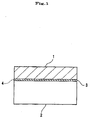
- Such proposals include, for instance, as shown in Fig. 3, a method for stabilizing the oxide/semiconductor interface, which comprises interposing a stable interface oxide (50) such as Y 2 O 3 , MgO, BiSiO 3 , etc., between a functional oxide (1) such as BaTiO 3 or SrTiO 3 , etc., and the semiconductor (2) such as a Si substrate.
- a stable interface oxide such as Y 2 O 3 , MgO, BiSiO 3 , etc.
- a functional oxide (1) such as BaTiO 3 or SrTiO 3 , etc.
- the semiconductor (2) such as a Si substrate.
- the stabilization is realized by the bonding that is formed between the elements constituting the interface oxide (50) and the dangling bonds of the elements constituting the semiconductor (2).
- Fig. 4 (A) shows schematically a part of the structure of a clean (001) surface of semiconductor Si that is highly reactive, because the outermost surface of the semiconductor Si consists of Si dimers having dangling bonds that are filled with two electrons and those having no electrons. Hence, an interface layer is formed between the semiconductor and the interface oxide as a result.
- an Object of the invention of the present application is to provide a method of stabilizing the oxide/semiconductor interface independent to temperature, which yet sufficiently realizes the performance of the functional oxide without forming an interface layer (reaction layer) between a semiconductor and the interface oxide, and to provide a stabilized semiconductor.
- the invention of the present application provides, in a first aspect, a method of stabilizing an oxide-semiconductor interface by using a Group 5 element, which comprises supplying an elemental Group 5 element or two or more types of Group 5 element to the surface of a semiconductor and growing an oxide on said Group 5 element, thereby stabilizing the interface between the oxide and the semiconductor.
- the invention of the present application provides, in a second aspect, a method of stabilizing an oxide-semiconductor interface by using a Group 5 element, wherein the semiconductor is silicon, the Group 5 element is As, and the oxide grown on the Group 5 element is a functional oxide such as CeO 2 , BaTiO 3 , PbZrTiO 3 , or SrTiO 3 .
- the invention of the present application provides, in a third aspect, a stabilized semiconductor the oxide-semiconductor interface thereof is stabilized by using a Group 5 element, in which the interface between the oxide and the semiconductor is stabilized by an oxide being grown on the surface of the semiconductor with an elemental Group 5 element or two or more types of Group 5 element being incorporated between them.
- the inventors of the present application extensively conducted studies, and, as a result, they have found that, by terminating the surface of the semiconductor with a Group 5 element, a surface structure having extremely low reactivity can be formed at the interface between the oxide and the semiconductor.
- the present invention has been accomplished based on these findings.
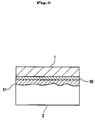
- a Group 5 element is supplied to the surface of a semiconductor (2) to cover the surface of the semiconductor with a coating layer (3) containing the Group 5 element, and a functional oxide (1) is grown thereon to stabilize an interface (4) between the oxide and the semiconductor.
- the method for supplying the Group 5 element to the surface of the semiconductor (2) is not particularly limited; for instance, a molecular beam of the Group 5 element may be supplied to the surface of the semiconductor after cleaning the surface by heating the semiconductor substrate in ultra-high vacuum, so that dimers of the Group 5 element may constitute the surface.
- any semiconductor (1) can be used without any particular limitation, and any type of semiconductors may be employed, e.g., the Group IV elements such as silicon, germanium, etc.; the Group III-VI compounds such as GaAs, InP, etc.; a hetero semiconductor; a piezo semiconductor; etc.
- the Group IV elements such as silicon, germanium, etc.
- the Group III-VI compounds such as GaAs, InP, etc.
- a hetero semiconductor such as GaAs, InP, etc.
- a piezo semiconductor etc.
- Group 5 element for use in the present invention, and there may be used Group 5A elements such as V, Nb, Ta, etc., as well as Group 5B elements such as N, P, As, Sb, Bi, etc.
- the Group 5 elements enumerated above may be used in the elemental form, but two or more types thereof may be supplied as well.
- a functional oxide (1) to be formed on the coating layer (3) using a Group 5 element in the present invention there maybe grown a dielectric material such as BaTiO 3 , SrTiO 3 , PbZrTiO 3 , etc., or a lattice matching oxide such as CeO 2 .
- a dielectric material such as BaTiO 3 , SrTiO 3 , PbZrTiO 3 , etc.
- a lattice matching oxide such as CeO 2 .
- the method according to the present invention greatly differs from a conventional one in that the oxide-semiconductor interface is stabilized by covering the surface of the semiconductor with a Group 5 element at a thickness of about 1 atomic layer.
- the performance of the functional oxide can be sufficiently exhibited yet without losing its function, because an interface layer (reaction layer) is not formed between the semiconductor and the interface oxide, but a stable oxide-semiconductor interface is established.
- a stable oxide-semiconductor interface can be formed independent to temperature.
- the invention according to the present invention is applicable in stably forming capacitors for use in memories of next generation integrated circuits, which, as a result, enables the implementation of a power-saving high-speed ferroelectric memory device capable of realizing high degree of integration, an application to an ultra-thin oxide film-semiconductor interface having a high dielectric Constant or a gate oxide film, an oxide-semiconductor superlattice, and a high efficiency light-emitting device.
- the stability of the oxide-semiconductor interface is described below by referring to its atomic structure.
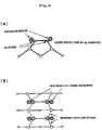
- Fig. 2 (A) there is shown a surface structure in atomic scale of a (001) surface of a semiconductor, silicon (Si), covered with a Group 5 element, arsenic (As) . Dimers of As constitute the outermost surface of the semiconductor, and the dangling bonds of the dimers are filled with two electrons. Hence, the reactivity of the surface of As is lost. Thus, in the present invention as a result, which is greatly different from the conventional methods of stabilization, no interface layer (reaction layer) is formed between the semiconductor and the interface oxide.
- the atomic bonding of the As dimers (5) in the outermost layer with the Si atoms (6) in the lower layers is very strong, and this bonding is formed on the surface as a group of four atomic bonds. Hence, the resulting surface exhibits less reactivity. This results in a stabilized oxide-semiconductor interface.
- the surface stress can be relaxed by forming an As dimer having a long bonding length.
- the bonding between the As dimers and the Si atoms in the lower layer results with less strain, and the bonding is maintained to higher temperatures independent to the temperature. This greatly contributes to the stabilization of an oxide-semiconductor interface.
- a Si (001) substrate which is used as the semiconductor, was heated in ultrahigh vacuum to form a clean (001) surface. Then, by supplying a Group 5 element in the form of an As molecular beam on the surface of the semiconductor, a 2 ⁇ 1 structure of Si (001):As constructed from dimers of a Group 5 element, i.e., As, was formed on the semiconductor substrate. Then, CeO 2 was grown on the thus obtained sample as a functional oxide at a substrate temperature of 300 °C. For comparison, CeO 2 was grown on a cleaned surface of Si at the same temperature.
- the invention provides a method for stabilizing an oxide-semiconductor interface, which is free from the formation of an interface layer (reactive layer) between a semiconductor and an interface oxide and which thereby allows satisfactory exhibition of performance capabilities of a functional oxide and achievement of the stability of oxide-semiconductor interface, yet independent of temperature; it also provides a stabilized semiconductor, and a stabilized semiconductor implemented by the above method.
- the invention according to the present invention is applicable to the stable formation of capacitors for use in memories of next generation integrated circuits, which, as a result, enables the implementation of a power-saving high-speed ferroelectric memory device capable of high degree of integration, an application to an ultra-thin oxide film-semiconductor interface having a high dielectric constant or a gate oxide film, an oxide-semiconductor superlattice, and a high efficiency light-emitting device.
Abstract
Description
- The present invention relates to a method for stabilizing an oxide-semiconductor interface by using a Group 5 element and to a stabilized semiconductor. In further detail, the invention of the present application provides a method for stabilizing an oxide-semiconductor interface and a stabilized semiconductor, which are useful in highly integrated circuits, ferroelectric materials, ferroelectric memories, etc.
- Extensive research and development have been made heretofore on realizing integrated circuits (referred to hereinafter as "ICs") with yet higher degree of integration and on realizing ferroelectric ICs. As a means of implementing such ICs with higher integration and ferroelectric ICs, there is established a method comprising forming an oxide film on the surface of a semiconductor such as a silicon to obtain a semiconductor oxide film.
- However, the interface between the semiconductor and the oxide film thus formed by a conventional method is extremely unstable, and hence, various reactions were found to occur as to result in unavoidable problems such as an increase in leak current, a malfunction of capacitors, etc.
- The problem of such an unstable oxide/semiconductor interface not only concerns the conventionally known electronic components, but also is a severe problem on realizing ferroelectric memories that are attracting much attention as an ultimate memory structure in near future. No solution of overcoming such an unstable oxide/semiconductor interface is found to present, and this has been the obstacle in implementing a ferroelectric memory. Very recently, however, some methods of stabilizing the oxide/semiconductor interface are being proposed to solve the problem of unstable oxide/semiconductor interface.
- Such proposals include, for instance, as shown in Fig. 3, a method for stabilizing the oxide/semiconductor interface, which comprises interposing a stable interface oxide (50) such as Y2O3, MgO, BiSiO3, etc., between a functional oxide (1) such as BaTiO3 or SrTiO3, etc., and the semiconductor (2) such as a Si substrate.
- However, in the case of a known method for stabilizing the oxide/semiconductor interface as shown in Fig. 3, an interface layer (a reaction layer) (51), although being thin, was found to be formed between the semiconductor (2) and the interface oxide (50), which unavoidably resulted in a semiconductor with impaired function.
- Furthermore, since two types of oxides, namely, the functional oxide (1) and the interface oxide (50), are laminated, there was found another severe problem of causing insufficient exhibition of the intrinsic performance of the functional oxide (1).
- Considering the stabilization behavior of the oxide/semiconductor interface in atomic level, the stabilization is realized by the bonding that is formed between the elements constituting the interface oxide (50) and the dangling bonds of the elements constituting the semiconductor (2). For instance, Fig. 4 (A) shows schematically a part of the structure of a clean (001) surface of semiconductor Si that is highly reactive, because the outermost surface of the semiconductor Si consists of Si dimers having dangling bonds that are filled with two electrons and those having no electrons. Hence, an interface layer is formed between the semiconductor and the interface oxide as a result.
- Furthermore referring to Fig. 4 (B), on considering the bonding between the Si dimers (53) in the outermost layer and the Si atoms (52) in the lower layers in the atomic level, it can be understood that the bond is highly stressed by the strain applied thereto. Thus, if seen in atomic level, the bonding between the Si dimers (53) in the outermost layer and the Si atoms (52) in the lower layers easily causes breakage at low temperatures. Hence, theoretically, the oxide/semiconductor interface can be stabilized at super low temperatures. In practice, however, the stabilization of the oxide/semiconductor interface was found to be extremely difficult.
- Conclusively, no methods capable of stabilizing the oxide/semiconductor interface independent to temperature while sufficiently exhibiting the performance of the functional oxide without allowing the formation of an interface layer (reaction layer) between a semiconductor and the interface oxide, nor a stabilized semiconductor, are realized to present.
- In the light of the aforementioned circumstances, an Object of the invention of the present application is to provide a method of stabilizing the oxide/semiconductor interface independent to temperature, which yet sufficiently realizes the performance of the functional oxide without forming an interface layer (reaction layer) between a semiconductor and the interface oxide, and to provide a stabilized semiconductor.
- As a means of overcoming the aforementioned problems, the invention of the present application provides, in a first aspect, a method of stabilizing an oxide-semiconductor interface by using a Group 5 element, which comprises supplying an elemental Group 5 element or two or more types of Group 5 element to the surface of a semiconductor and growing an oxide on said Group 5 element, thereby stabilizing the interface between the oxide and the semiconductor.
- Furthermore, the invention of the present application provides, in a second aspect, a method of stabilizing an oxide-semiconductor interface by using a Group 5 element, wherein the semiconductor is silicon, the Group 5 element is As, and the oxide grown on the Group 5 element is a functional oxide such as CeO2, BaTiO3, PbZrTiO3, or SrTiO3.
- Additionally, the invention of the present application provides, in a third aspect, a stabilized semiconductor the oxide-semiconductor interface thereof is stabilized by using a Group 5 element, in which the interface between the oxide and the semiconductor is stabilized by an oxide being grown on the surface of the semiconductor with an elemental Group 5 element or two or more types of Group 5 element being incorporated between them.
- That is, the inventors of the present application extensively conducted studies, and, as a result, they have found that, by terminating the surface of the semiconductor with a Group 5 element, a surface structure having extremely low reactivity can be formed at the interface between the oxide and the semiconductor. The present invention has been accomplished based on these findings.
-
- Fig. 1 is a schematically drawn cross section showing an example of a semiconductor formed by a method according to the invention of the present application;
- Figs. 2 (A) and 2 (B) are each a schematically drawn diagram showing the behavior of atoms in carrying out the method of the invention according to the present application;
- Fig. 3 is a schematically drawn cross section showing a semiconductor formed by a prior art method;
- Figs. 4 (A) and 4 (B) are each a schematically drawn diagram showing the behavior of atoms in carrying out a conventional method;
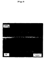
- Fig. 5 is a high resolution transmission electron micrograph of a CeO2/Si interface covered with As; it reads that the continuity of the lattice at the CeO2/Si interface is obtained, and that an acute interface is formed;
- Fig. 6 is a high resolution transmission electron micrograph of a CeO2/Si interface not covered with As; the formation of about 10 nm thick amorphous interface layer can be observed at the CeO2/Si interface.
-
- An embodiment of a novel method of stabilizing an oxide-semiconductor interface and a novel type of stabilized semiconductor according to the invention of the present application are shown, for instance, in Fig. 1. More specifically, a Group 5 element is supplied to the surface of a semiconductor (2) to cover the surface of the semiconductor with a coating layer (3) containing the Group 5 element, and a functional oxide (1) is grown thereon to stabilize an interface (4) between the oxide and the semiconductor.
- In the present invention, the method for supplying the Group 5 element to the surface of the semiconductor (2) is not particularly limited; for instance, a molecular beam of the Group 5 element may be supplied to the surface of the semiconductor after cleaning the surface by heating the semiconductor substrate in ultra-high vacuum, so that dimers of the Group 5 element may constitute the surface.
- in the present invention, any semiconductor (1) can be used without any particular limitation, and any type of semiconductors may be employed, e.g., the Group IV elements such as silicon, germanium, etc.; the Group III-VI compounds such as GaAs, InP, etc.; a hetero semiconductor; a piezo semiconductor; etc.
- There is no particular limitation on the Group 5 element for use in the present invention, and there may be used Group 5A elements such as V, Nb, Ta, etc., as well as Group 5B elements such as N, P, As, Sb, Bi, etc.
- The Group 5 elements enumerated above may be used in the elemental form, but two or more types thereof may be supplied as well.
- As a functional oxide (1) to be formed on the coating layer (3) using a Group 5 element in the present invention, there maybe grown a dielectric material such as BaTiO3, SrTiO3, PbZrTiO3, etc., or a lattice matching oxide such as CeO2. By using such functional oxides (1), a sharply distinguished oxide-semiconductor interface can be implemented.
- The method according to the present invention greatly differs from a conventional one in that the oxide-semiconductor interface is stabilized by covering the surface of the semiconductor with a Group 5 element at a thickness of about 1 atomic layer. Thus, the performance of the functional oxide can be sufficiently exhibited yet without losing its function, because an interface layer (reaction layer) is not formed between the semiconductor and the interface oxide, but a stable oxide-semiconductor interface is established. Furthermore, as is described hereinafter, a stable oxide-semiconductor interface can be formed independent to temperature.
- Conclusively, the invention according to the present invention is applicable in stably forming capacitors for use in memories of next generation integrated circuits, which, as a result, enables the implementation of a power-saving high-speed ferroelectric memory device capable of realizing high degree of integration, an application to an ultra-thin oxide film-semiconductor interface having a high dielectric Constant or a gate oxide film, an oxide-semiconductor superlattice, and a high efficiency light-emitting device.
- The stability of the oxide-semiconductor interface is described below by referring to its atomic structure.
- Referring to Fig. 2 (A), there is shown a surface structure in atomic scale of a (001) surface of a semiconductor, silicon (Si), covered with a Group 5 element, arsenic (As) . Dimers of As constitute the outermost surface of the semiconductor, and the dangling bonds of the dimers are filled with two electrons. Hence, the reactivity of the surface of As is lost. Thus, in the present invention as a result, which is greatly different from the conventional methods of stabilization, no interface layer (reaction layer) is formed between the semiconductor and the interface oxide.
- Further referring to Fig. 2 (B), the atomic bonding of the As dimers (5) in the outermost layer with the Si atoms (6) in the lower layers is very strong, and this bonding is formed on the surface as a group of four atomic bonds. Hence, the resulting surface exhibits less reactivity. This results in a stabilized oxide-semiconductor interface.
- Furthermore, the surface stress can be relaxed by forming an As dimer having a long bonding length. Thus, the bonding between the As dimers and the Si atoms in the lower layer results with less strain, and the bonding is maintained to higher temperatures independent to the temperature. This greatly contributes to the stabilization of an oxide-semiconductor interface.
- The present invention is described in further detail below by making reference to Examples.
- First, a Si (001) substrate, which is used as the semiconductor, was heated in ultrahigh vacuum to form a clean (001) surface. Then, by supplying a Group 5 element in the form of an As molecular beam on the surface of the semiconductor, a 2 × 1 structure of Si (001):As constructed from dimers of a Group 5 element, i.e., As, was formed on the semiconductor substrate. Then, CeO2 was grown on the thus obtained sample as a functional oxide at a substrate temperature of 300 °C. For comparison, CeO2 was grown on a cleaned surface of Si at the same temperature.
- On observing the interface structure between the semiconductor and the functional oxide, as shown in Fig. 5, a continuous lattice was found to be formed on the CeO2/Si interface to which the Group 5 element As had been supplied; however, as shown in Fig. 6, the formation of about 10 nm thick reaction layer was observed on the CeO2/Si interface to which no As was supplied as the Group 5 element.
- From the results above, the surface treatment of silicon by using a Group 5 element was found to be effective in forming a sharp oxide/silicon interface.
- As a matter of course, the present invention is not only limited to the example above, but various modifications can be made on the details.
- As described in detail above, the invention according to the present application provides a method for stabilizing an oxide-semiconductor interface, which is free from the formation of an interface layer (reactive layer) between a semiconductor and an interface oxide and which thereby allows satisfactory exhibition of performance capabilities of a functional oxide and achievement of the stability of oxide-semiconductor interface, yet independent of temperature; it also provides a stabilized semiconductor, and a stabilized semiconductor implemented by the above method.
- Conclusively, the invention according to the present invention is applicable to the stable formation of capacitors for use in memories of next generation integrated circuits, which, as a result, enables the implementation of a power-saving high-speed ferroelectric memory device capable of high degree of integration, an application to an ultra-thin oxide film-semiconductor interface having a high dielectric constant or a gate oxide film, an oxide-semiconductor superlattice, and a high efficiency light-emitting device.
Claims (3)
- A method of stabilizing an oxide-semiconductor interface by using a Group 5 element, which comprises supplying an elemental Group 5 element or two or more types of Group 5 element to the surface of a semiconductor and growing an oxide on said Group 5 element, thereby stabilizing the interface between the oxide and the semiconductor.
- A stabilizing method as claimed in claim 1, wherein the semiconductor is silicon, the Group 5 element is As, and the oxide grown on the Group 5 element is CeO2, BaTiO3, PbZrTiO3, or SrTiO3.
- A stabilized semiconductor the oxide-semiconductor interface thereof is stabilized by using a Group 5 element, in which the interface between the oxide and the semiconductor is stabilized by an oxide being grown on the surface of the semiconductor with an elemental Group 5 element or two or more types of Group 5 element being incorporated between them.
Applications Claiming Priority (3)
| Application Number | Priority Date | Filing Date | Title |
|---|---|---|---|
| JP32222799A JP2001144087A (en) | 1999-11-12 | 1999-11-12 | Method of stabilizing interface between oxide and semiconductor by group v element and stabilized semiconductor |
| JP32222799 | 1999-11-12 | ||
| PCT/JP2000/007940 WO2001037330A1 (en) | 1999-11-12 | 2000-11-10 | Method for stabilizing oxide-semiconductor interface by using group 5 element and stabilized semiconductor |
Publications (3)
| Publication Number | Publication Date |
|---|---|
| EP1237183A1 true EP1237183A1 (en) | 2002-09-04 |
| EP1237183A4 EP1237183A4 (en) | 2006-02-15 |
| EP1237183B1 EP1237183B1 (en) | 2011-01-19 |
Family
ID=18141363
Family Applications (1)
| Application Number | Title | Priority Date | Filing Date |
|---|---|---|---|
| EP00974913A Expired - Lifetime EP1237183B1 (en) | 1999-11-12 | 2000-11-10 | Method for stabilizing oxide-semiconductor interface by using group 5 element and stabilized semiconductor |
Country Status (7)
| Country | Link |
|---|---|
| US (1) | US6723164B1 (en) |
| EP (1) | EP1237183B1 (en) |
| JP (1) | JP2001144087A (en) |
| KR (1) | KR100518395B1 (en) |
| DE (1) | DE60045559D1 (en) |
| TW (1) | TW490762B (en) |
| WO (1) | WO2001037330A1 (en) |
Cited By (1)
| Publication number | Priority date | Publication date | Assignee | Title |
|---|---|---|---|---|
| WO2012042442A1 (en) * | 2010-09-28 | 2012-04-05 | International Business Machines Corporation | Semiconductor device with a gate stack |
Families Citing this family (2)
| Publication number | Priority date | Publication date | Assignee | Title |
|---|---|---|---|---|
| TW497209B (en) * | 2000-07-21 | 2002-08-01 | Motorola Inc | Method for and structure of alkali earth metal oxide on gate insulators |
| DE112005002798T5 (en) * | 2004-11-10 | 2007-09-27 | Dai Nippon Printing Co., Ltd. | Process for the preparation of a metal oxide film |
Citations (2)
| Publication number | Priority date | Publication date | Assignee | Title |
|---|---|---|---|---|
| US5527567A (en) * | 1994-09-02 | 1996-06-18 | Ceram Incorporated | Metalorganic chemical vapor deposition of layered structure oxides |
| JPH11224947A (en) * | 1997-11-28 | 1999-08-17 | Toshiba Corp | Semiconductor device and manufacture thereof |
Family Cites Families (7)
| Publication number | Priority date | Publication date | Assignee | Title |
|---|---|---|---|---|
| JPH0614050A (en) | 1992-03-18 | 1994-01-21 | Fujitsu Ltd | Call interruption method in atm network and exchange implementing the method |
| US5920775A (en) * | 1996-02-23 | 1999-07-06 | Vanguard International Semiconductor Corporation | Method for forming a storage capacitor within an integrated circuit |
| JPH10231196A (en) | 1996-12-17 | 1998-09-02 | Sony Corp | Production of oxide laminated structure, and apparatus for chemical vapor-phase growth of organic metal compound |
| US6087208A (en) * | 1998-03-31 | 2000-07-11 | Advanced Micro Devices, Inc. | Method for increasing gate capacitance by using both high and low dielectric gate material |
| KR100297719B1 (en) * | 1998-10-16 | 2001-08-07 | 윤종용 | Method for manufacturing thin film |
| JP2000183295A (en) | 1998-12-16 | 2000-06-30 | Matsushita Electronics Industry Corp | Semiconductor storage and its manufacture |
| US20030015704A1 (en) * | 2001-07-23 | 2003-01-23 | Motorola, Inc. | Structure and process for fabricating semiconductor structures and devices utilizing the formation of a compliant substrate for materials used to form the same including intermediate surface cleaning |
-
1999
- 1999-11-12 JP JP32222799A patent/JP2001144087A/en active Pending
-
2000
- 2000-11-10 WO PCT/JP2000/007940 patent/WO2001037330A1/en active IP Right Grant
- 2000-11-10 TW TW089123758A patent/TW490762B/en not_active IP Right Cessation
- 2000-11-10 EP EP00974913A patent/EP1237183B1/en not_active Expired - Lifetime
- 2000-11-10 KR KR10-2002-7006120A patent/KR100518395B1/en not_active IP Right Cessation
- 2000-11-10 DE DE60045559T patent/DE60045559D1/en not_active Expired - Lifetime
- 2000-11-10 US US10/129,983 patent/US6723164B1/en not_active Expired - Fee Related
Patent Citations (2)
| Publication number | Priority date | Publication date | Assignee | Title |
|---|---|---|---|---|
| US5527567A (en) * | 1994-09-02 | 1996-06-18 | Ceram Incorporated | Metalorganic chemical vapor deposition of layered structure oxides |
| JPH11224947A (en) * | 1997-11-28 | 1999-08-17 | Toshiba Corp | Semiconductor device and manufacture thereof |
Non-Patent Citations (5)
| Title |
|---|
| HIRAI T ET AL: "FORMATION OF METAL/FERROELECTRIC/INSULATOR/SEMICONDUCTO R STRUCTURE WITH A CEO2 BUFFER LAYER" JAPANESE JOURNAL OF APPLIED PHYSICS, JAPAN SOCIETY OF APPLIED PHYSICS, TOKYO, JP, vol. 33, no. 9B, PART 1, 1 September 1994 (1994-09-01), pages 5219-5222, XP000595096 ISSN: 0021-4922 * |
| HIRAI T ET AL: "PREPARATION OF SRBI2TA2O9 FILM AT LOW TEMPERATURES AND FABRICATION OF A METAL/FERROELECTRIC/INSULATOR/SEMICONDUCTO R FIELD EFFECT TRANSISTOR USING AL/SRBI2TA2O9/CEO2/SI(100) STRUCTURES" JAPANESE JOURNAL OF APPLIED PHYSICS, JAPAN SOCIETY OF APPLIED PHYSICS, TOKYO, JP, vol. 36, no. 9B, PART 1, September 1997 (1997-09), pages 5908-5911, XP000824028 ISSN: 0021-4922 * |
| PATENT ABSTRACTS OF JAPAN vol. 1999, no. 13, 30 November 1999 (1999-11-30) -& JP 11 224947 A (TOSHIBA CORP), 17 August 1999 (1999-08-17) * |
| See also references of WO0137330A1 * |
| ZHOU XIAOCHUAN ET AL: "Epitaxial growth of ZnS on bare and arsenic-passivated vicinal Si(100) surfaces" JOURNAL OF APPLIED PHYSICS, AMERICAN INSTITUTE OF PHYSICS. NEW YORK, US, vol. 82, no. 5, 1 September 1997 (1997-09-01), page 2251, XP012043312 ISSN: 0021-8979 * |
Cited By (3)
| Publication number | Priority date | Publication date | Assignee | Title |
|---|---|---|---|---|
| WO2012042442A1 (en) * | 2010-09-28 | 2012-04-05 | International Business Machines Corporation | Semiconductor device with a gate stack |
| GB2497257A (en) * | 2010-09-28 | 2013-06-05 | Ibm | Semiconductor device with a gate stack |
| GB2497257B (en) * | 2010-09-28 | 2013-11-06 | Ibm | Semiconductor device with a gate stack |
Also Published As
| Publication number | Publication date |
|---|---|
| EP1237183A4 (en) | 2006-02-15 |
| JP2001144087A (en) | 2001-05-25 |
| DE60045559D1 (en) | 2011-03-03 |
| US6723164B1 (en) | 2004-04-20 |
| EP1237183B1 (en) | 2011-01-19 |
| KR100518395B1 (en) | 2005-09-29 |
| KR20020085891A (en) | 2002-11-16 |
| TW490762B (en) | 2002-06-11 |
| WO2001037330A1 (en) | 2001-05-25 |
Similar Documents
| Publication | Publication Date | Title |
|---|---|---|
| KR100676213B1 (en) | Method for fabricating a semiconductor structure having a stable crystalline interface with silicon | |
| US6248459B1 (en) | Semiconductor structure having a crystalline alkaline earth metal oxide interface with silicon | |
| US7199015B2 (en) | Rare earth-oxides, rare earth-nitrides, rare earth-phosphides and ternary alloys with silicon | |
| US7645517B2 (en) | Rare earth-oxides, rare earth nitrides, rare earth phosphides and ternary alloys with silicon | |
| US5051786A (en) | Passivated polycrystalline semiconductors quantum well/superlattice structures fabricated thereof | |
| EP1043426A1 (en) | Method for fabricating a semiconductor structure having a single atomic layer with alkaline earth metal metal, oxygen and silicon at the interface between a silicon substrate and a single crystal oxide layer | |
| WO2002041378A2 (en) | Semiconductor structure and process for fabricating same | |
| Wang et al. | Interface and tunneling barrier heights of NbN/AlN/NbN tunnel junctions | |
| KR20010062134A (en) | Semiconductor structure having a crystalline alkaline earth metal silicon nitride/oxide interface with silicon | |
| WO2002058164A2 (en) | Gan layer on a substrate with an amorphous layer | |
| JPH10289906A (en) | Manufacture of group iii-v epitaxial wafer | |
| KR100516252B1 (en) | ARTICLE COMPRISING AN OXIDE LAYER ON GaN, AND METHOD OF MAKING THE ARTICLE | |
| US6723164B1 (en) | Method for stabilizing oxide-semiconductor interface by using group 5 element and stabilized semiconductor | |
| US7045815B2 (en) | Semiconductor structure exhibiting reduced leakage current and method of fabricating same | |
| Martrou et al. | Equilibrium shape of steps and islands on polar II-VI semiconductors surfaces | |
| US7678633B2 (en) | Method for forming substrates for MOS transistor components and its products | |
| Kim et al. | Microstructural and electrical properties of MgO thin films grown on p-InP (100) substrates at low temperature | |
| EP1315852A1 (en) | Epitaxial wafer apparatus | |
| TW507317B (en) | Semiconductor structure having high dielectric constant material | |
| Oral et al. | Initial stages of SiGe epitaxy on Si (001) studied by scanning tunneling microscopy | |
| US20030034500A1 (en) | Semiconductor structure including a zintl material buffer layer, device including the structure, and method of forming the structure and device | |
| Kim et al. | Microstructural and electrical properties of MgO thin films grown on p-GaAs (100) substrates | |
| Kubo et al. | Direct Observation of Strained Layer Formation at the Initial Stage of In Thin Film Growth on Si (100) | |
| TW526605B (en) | Method of forming an amorphous layer of a semiconductor structure using a high energy beam | |
| US20020163010A1 (en) | Wide bandgap semiconductor structure, semiconductor device including the structure, and methods of forming the structure and device |
Legal Events
| Date | Code | Title | Description |
|---|---|---|---|
| PUAI | Public reference made under article 153(3) epc to a published international application that has entered the european phase |
Free format text: ORIGINAL CODE: 0009012 |
|
| 17P | Request for examination filed |
Effective date: 20020612 |
|
| AK | Designated contracting states |
Kind code of ref document: A1 Designated state(s): AT BE CH CY DE DK ES FI FR GB GR IE IT LI LU MC NL PT SE TR |
|
| RBV | Designated contracting states (corrected) |
Designated state(s): AT BE CH CY DE FR GB LI NL |
|
| RAP1 | Party data changed (applicant data changed or rights of an application transferred) |
Owner name: JAPAN AS REPRESENTED BY DIRECTOR GENERAL OF NATION Owner name: JAPAN SCIENCE AND TECHNOLOGY AGENCY |
|
| A4 | Supplementary search report drawn up and despatched |
Effective date: 20060103 |
|
| RAP1 | Party data changed (applicant data changed or rights of an application transferred) |
Owner name: NATIONAL INSTITUTE FOR MATERIALS SCIENCE |
|
| GRAP | Despatch of communication of intention to grant a patent |
Free format text: ORIGINAL CODE: EPIDOSNIGR1 |
|
| GRAS | Grant fee paid |
Free format text: ORIGINAL CODE: EPIDOSNIGR3 |
|
| GRAA | (expected) grant |
Free format text: ORIGINAL CODE: 0009210 |
|
| AK | Designated contracting states |
Kind code of ref document: B1 Designated state(s): DE FR GB NL |
|
| REG | Reference to a national code |
Ref country code: GB Ref legal event code: FG4D |
|
| REF | Corresponds to: |
Ref document number: 60045559 Country of ref document: DE Date of ref document: 20110303 Kind code of ref document: P |
|
| REG | Reference to a national code |
Ref country code: DE Ref legal event code: R096 Ref document number: 60045559 Country of ref document: DE Effective date: 20110303 |
|
| REG | Reference to a national code |
Ref country code: NL Ref legal event code: T3 |
|
| PLBE | No opposition filed within time limit |
Free format text: ORIGINAL CODE: 0009261 |
|
| STAA | Information on the status of an ep patent application or granted ep patent |
Free format text: STATUS: NO OPPOSITION FILED WITHIN TIME LIMIT |
|
| 26N | No opposition filed |
Effective date: 20111020 |
|
| REG | Reference to a national code |
Ref country code: DE Ref legal event code: R097 Ref document number: 60045559 Country of ref document: DE Effective date: 20111020 |
|
| PGFP | Annual fee paid to national office [announced via postgrant information from national office to epo] |
Ref country code: FR Payment date: 20121130 Year of fee payment: 13 Ref country code: DE Payment date: 20121121 Year of fee payment: 13 |
|
| PGFP | Annual fee paid to national office [announced via postgrant information from national office to epo] |
Ref country code: GB Payment date: 20121120 Year of fee payment: 13 |
|
| PGFP | Annual fee paid to national office [announced via postgrant information from national office to epo] |
Ref country code: NL Payment date: 20121120 Year of fee payment: 13 |
|
| REG | Reference to a national code |
Ref country code: NL Ref legal event code: V1 Effective date: 20140601 |
|
| GBPC | Gb: european patent ceased through non-payment of renewal fee |
Effective date: 20131110 |
|
| REG | Reference to a national code |
Ref country code: FR Ref legal event code: ST Effective date: 20140731 |
|
| PG25 | Lapsed in a contracting state [announced via postgrant information from national office to epo] |
Ref country code: NL Free format text: LAPSE BECAUSE OF NON-PAYMENT OF DUE FEES Effective date: 20140601 Ref country code: DE Free format text: LAPSE BECAUSE OF NON-PAYMENT OF DUE FEES Effective date: 20140603 |
|
| REG | Reference to a national code |
Ref country code: DE Ref legal event code: R119 Ref document number: 60045559 Country of ref document: DE Effective date: 20140603 |
|
| PG25 | Lapsed in a contracting state [announced via postgrant information from national office to epo] |
Ref country code: GB Free format text: LAPSE BECAUSE OF NON-PAYMENT OF DUE FEES Effective date: 20131110 Ref country code: FR Free format text: LAPSE BECAUSE OF NON-PAYMENT OF DUE FEES Effective date: 20131202 |