EP1245982B1 - Vorrichtung zur Lagerung eines optischen Elementes in einer Optik - Google Patents
Vorrichtung zur Lagerung eines optischen Elementes in einer Optik Download PDFInfo
- Publication number
- EP1245982B1 EP1245982B1 EP02005695A EP02005695A EP1245982B1 EP 1245982 B1 EP1245982 B1 EP 1245982B1 EP 02005695 A EP02005695 A EP 02005695A EP 02005695 A EP02005695 A EP 02005695A EP 1245982 B1 EP1245982 B1 EP 1245982B1
- Authority
- EP
- European Patent Office
- Prior art keywords
- optical element
- parallelogram
- manipulators
- circumference
- optical
- Prior art date
- Legal status (The legal status is an assumption and is not a legal conclusion. Google has not performed a legal analysis and makes no representation as to the accuracy of the status listed.)
- Expired - Lifetime
Links
Images

Classifications
-
- G—PHYSICS
- G02—OPTICS
- G02B—OPTICAL ELEMENTS, SYSTEMS OR APPARATUS
- G02B7/00—Mountings, adjusting means, or light-tight connections, for optical elements
- G02B7/02—Mountings, adjusting means, or light-tight connections, for optical elements for lenses
- G02B7/023—Mountings, adjusting means, or light-tight connections, for optical elements for lenses permitting adjustment
Definitions
- the invention relates to a device for mounting an optical Element in an optic, in particular a mirror or a lens, in a projection exposure apparatus, in particular a projection objective in semiconductor lithography.
- Optical elements such as e.g. Mirrors and lenses, in optics, especially in semiconductor lithography, should be isostatic and thus be stored with decoupled decoupling so that external interference should be avoided affect optical element.
- the optical Store the element according to "soft". The problem with However, a soft storage is that you can not reached sufficiently high natural frequencies.
- EP 1 209 500 A2 as an earlier law describes a device for mounting an optical element in an assembly.
- the device has at least three at the periphery of the optical Elements arranged connection points on. Further points the device transmission elements, which each have a radially lying spiral spring via a head point to the optical Element is tethered.
- the transmission elements are included arranged or dimensioned so that they are at disturbances on the optical element a compensation effect in terms the deformation of the optical surface of the optical Element result.
- DE 199 10 947 A1 is also a device for storage or for moving an optical element along the optical axis revealed.
- the optical element is in one Retaining ring mounted on which an adjustment for Moving the optical element along the optical axis attacks.
- a support ring is about solid joints with the Retaining ring connected, with a high rigidity perpendicular to optical axis is achieved. In the axial direction, the Solid joints on a sufficient softness. through This device can be particularly large and heavy optical elements very precise in the direction of the optical Axis be moved without introducing lateral movements.
- the present invention is therefore based on the object a device for mounting an optical element to create on the one hand little or low forces on the optical Element, i. the very good deformation decoupling is, but on the other hand, a high natural frequency is reached.
- external disturbances should act no surface deformations on the optical element cause, if any, a whole body movement.
- the embodiment of the invention can be at relative compact design a rigid construction with resulting reach high natural frequencies.
- it can be to carry out the storage with few components, in the If necessary, a monolithic design is possible.
- the three storage facilities each two parallel to the z-direction (optical axis) at a distance from each other arranged in tangential direction extending bending members with an intermediate member arranged therebetween.
- Each storage device has in this way, e.g. two up Distance apart in the tangential direction the optical element extending leaf springs and one in radial Direction extending leaf spring as a transverse joint.
- the between the two running in the tangential direction Leaf springs arranged intermediate member may be stiff or also - in a very advantageous and not obvious Further development of the invention - designed as a manipulator device be.
- the intermediate member with a Adjustment direction for length change parallel to the z-direction be provided.
- One possible embodiment of this lies in a parallelogram-like Structure or a structure comparable to a scissors jack principle.
- the length can be the or the distributed over the circumference arranged intermediate links - with or without translation - very sensitively change. Be all intermediate links of the storage facilities evenly changed in length, so that is the optical element moved in z-direction. For individual changes in length can be tilted in this way, the optical element accordingly.
- the outer basic structure, with which the optical element is connected via the storage device via Manipulators with a fixed housing structure of the optics connected, wherein the manipulators on the housing structure support.
- the mirror is stored isostatically, wherein by the arrangement of the manipulators no negative change the natural frequency is reached. This causes their effect over the outer basic structure.
- the outer basic structure In the outer basic structure the moments and forces of the manipulators are initiated, whereby it does not affect the optical element to have. In practical terms, it is generally very stiff Basic structure for decoupling the restoring forces of the Manipulators.
- the manipulators are based on a fixed housing structure optics, which at the same time act as an interface structure, e.g. in ring form, can serve.
- the optical element in Define or adjust a lens defined.
- a lens defined is the actual position detected by the sensors, after which a desired position is set.
- the optional sensors which e.g. three over the Scope distributed arranged non-contact distance sensors be a direct and thus more accurate measurement, instead of a measurement via the travel of the manipulators.
- Non-contact distance sensors can the most diverse sensors are used.
- the mating surfaces may e.g. this on the optical Element vapor-deposited in an optically inactive area be.
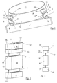
- An optical element e.g. a mirror 1 is uniform over three Distributed over the circumference arranged storage facilities. 2 connected to an outer basic structure 3.
- the basic structure 3 may be part of an optic, e.g. of a projection lens in be the semiconductor lithography.
- the illustrated triangular Form of the basic structure is merely an example. If necessary, other forms, such as e.g. a Circular shape possible.
- the storage facilities 2 are constructed so that they are very strong are decoupled from decoupling and thereby no external the basic structure 3 acting disturbances on the optical element Pass on 1.
- the basic structure is very stiff (ceramic is advantageous) to the forces coming from outside to decouple as well as possible from the bearing elements and the mirror. In this way, a double deformation decoupling reached.
- FIGs 2 to 3 is an enlarged view A first embodiment of a storage device 2 shown.
- the storage device is monolithic or integrally formed with solid joints between the individual moving parts. She has an upper one Mounting part 4, with which the storage device 2 via a pivot point 4a with a socket 5 of the optical element 1 is connected.
- the fastening part 4 also be connected directly to the optical element 1.
- a connecting part 6 On the Bottom or on the side remote from the articulation point 4a Side is the storage facility 2 via a connecting part 6 with connected to the basic structure 3.
- a first bending joint 7 connected in the form of a leaf spring 7, which tangentially to the frame 5 or the optical element 1 is arranged.
- the leaf spring 7 On the side remote from the connecting part 6 Side is the leaf spring 7 with a stiff intermediate member. 8 connected as Ausknicktik, which in turn on the of the Leaf spring 7 opposite side with a further bending member 9, also in the form of a leaf spring connected.
- the leaf spring 9 also extends tangentially with its longitudinal axis to the version 5 or the optical element 1.
- the leaf spring. 9 is on the side remote from the intermediate member 8 side with a Transition plate 10 connected.
- the transition plate 10 is over a in the radial direction - with respect to the optical element - extending bending member 11 as a transverse joint with the fastening part 4 connected.
- leaf spring 7 via a solid-state joint 12 with the connecting part 6 and a solid-state joint 13 connected to the intermediate member 8.
- leaf spring 9 via a solid-state joint 14 with the intermediate member 8 and a solid joint 15 with the transition plate 10 connected.
- the bending member 11 acts due to its small axial extent overall like a solid-state joint 17.
- a larger axial extent possible same for vice versa for the two leaf springs 7 and 9.
- the storage facilities 2 are both individually as well as together by manipulators, not shown axially displaceable, in which case the shift - accordingly the direction of attack - on the responsive leaf springs 7, 9 or the bending member 11 and the solid state joints the optical element 1 is passed.
- manipulators not shown axially displaceable, in which case the shift - accordingly the direction of attack - on the responsive leaf springs 7, 9 or the bending member 11 and the solid state joints the optical element 1 is passed.
- this configuration practically every storage facility 2 is a gimbal Suspension for element 1. Due to the solid state joints but is sufficient rigidity against natural frequencies given.
- FIG. 4 shows an embodiment of a bearing device 2 in another embodiment.
- the only difference is that the rigid intermediate member 8 by a parallelogram with the four Pages 8a, 8b, 8c and 8d has been replaced.
- the one-sided located parallelogram pages 8a and 8b are through Solid joints 18 and 19 connected together.
- an actuator member 20 In each case between the solid joints 18 and 19 is an actuator member 20.
- the adjustment movement can be linearized be by optimizing the opening angle ⁇ and ⁇ .
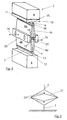
- FIG. 6 is a development of the invention represented, wherein the optical element 1 by three evenly distributed around the circumference arranged manipulators 24 in axial direction is adjustable.
- a sensor device shown with the respective position of the optical element 1 is exactly verifiable.
- FIGS Manipulators 24 on a fixed housing structure 25 of the Optics, e.g. an only partially shown lens 26, from. As can be seen, they act on the housing structure 25 supporting manipulators 24 on the base structure 3 on the Bearing device 2 (in the figure 8 for simplicity only in principle represented) and thus on the optical element 1. Da the basic structure 3 can be made very rigid, e.g. out ceramic material, it can be used to decouple the restoring forces serve the manipulators 24.
- the manipulators 24 are only in principle in the figures 6 to 8 indicated, since this is the most diverse engines or Adjustment devices, the axial length changes according to arrow Generate 27, are used arbitrarily. Thus, e.g. piezoceramic Actuators that change the length of a voltage application experienced, possible.
- the manipulators 24, the on one side with the housing structure 25 and on the other side are connected to the basic structure 3, e.g. each through an opening 28 in the region of the corners of the triangular Basic structure 3 are used from below (see FIG 7).
- the stationary housing structure 25 e.g. three distributed over the circumference arranged sensors 29 are provided.
- the sensors 29 cooperate with counter-members 30 which on the optical element 1 outside the optically effective range are arranged correspondingly opposite.
- the non-contact act As sensor devices, e.g. capacitive sensors or use distance interferometers, the non-contact act.
- the counter-members 30 on the optical element 1 can thereby vapor-deposited as conductive mating surfaces on the optical element 1 be.
Description
- Figur 1
- eine perspektivische Darstellung der erfindungsgemäßen Vorrichtung zur Lagerung eines optischen Elementes,
- Figur 2
- eine Lagereinrichtung in perspektivischer und vergrößerter Darstellung,
- Figur 3
- eine Seitenansicht der Lagereinrichtung aus Pfeilrichtung A in der Figur 1,
- Figur 4
- eine Lagereinrichtung in perspektivischer und vergrößerter Darstellung in einer anderen Ausführungsform,
- Figur 5
- eine Prinzipdarstellung einer Lagereinrichtung in einer dritten Ausführungsform,
- Figur 6
- eine perspektivische Ansicht des optischen Elementes mit der Lagereinrichtung und mit Manipulatoren (ohne feststehende Gehäusestruktur) von oben,
- Figur 7
- eine perspektivische Ansicht der erfindungsgemäßen Vorrichtung nach der Figur 6 von unten, und
- Figur 8
- einen Schnitt durch die Vorrichtung nach den Figuren 6 und 7 mit einer feststehenden Gehäusestruktur zur Abstützung der Manipulatoren und mit einer Sensoreinrichtung.
Claims (18)
- Vorrichtung zur Lagerung eines optischen Elementes (1) in einer Optik, insbesondere eines Spiegels oder einer Linse, in einer Projektionsbelichtungsanlage, insbesondere einem Projektionsobjektiv in der Halbleiter-Lithographie, mit wenigstens drei am Umfang des optischen Elementes (1) angeordneten Anlenkstellen (4a), an denen jeweils eine Lagereinrichtung (2) mit wenigstens einem blattfederartigen Biegeglied, welches auf der von der Anlenkstelle (4a) abgewandten Seite mit einer äußeren Grundstruktur (3) verbunden ist, dadurch gekennzeichnet, dass die Lagereinrichtung (2) zwei parallel zur optischen Achse auf Abstand voneinander angeordnete in tangentialer Richtung zu dem optischen Element (1) verlaufende blattfederartige Biegeglieder (7,9) mit einem dazwischen angeordneten Zwischenglied (8) und wenigstens ein in radialer Richtung zu dem optischen Element angeordnetes blattfederartiges Bindeglied (11) aufweist.
- Vorrichtung nach Anspruch 1, dadurch gekennzeichnet, dass die Biegeglieder (7,9,11) jeweils über Festkörpergelenke (12,13,14,15,17) mit den benachbart liegenden Teilen, wie Anlenkstelle (4a), Verbindungsteile (6), Zwischenglieder (8), Übergangsplatte (10), verbunden sind.
- Vorrichtung nach einem der Ansprüche 1, dadurch gekennzeichnet, dass das Zwischenglied (8) mit einer Verstelleinrichtung (16) zur Längenänderung des Zwischengliedes (8) parallel zur optischen Achse versehen ist.
- Vorrichtung nach Anspruch 3, dadurch gekennzeichnet, dass die Verstelleinrichtung wenigstens eine parallelogrammartige Form (8a,8b,8c,8d) aufweist, deren Öffnungswinkel (α) durch die Verstelleinrichtung (16) verstellbar ist.
- Vorrichtung nach Anspruch 4, dadurch gekennzeichnet, dass die parallelogrammartigen Seiten (8a,8b,8c,8d) jeweils über Festkörpergelenke (12,13,14,15,17) miteinander verbunden sind.
- Vorrichtung nach Anspruch 5, dadurch gekennzeichnet, dass jeweils zwischen den auf einer Seite sich befindenden Parallelogrammseiten (8a,8b bzw. 8c,8d) ein Aktuatorglied (20) angreift.
- Vorrichtung nach Anspruch 4, dadurch gekennzeichnet, dass im Inneren des Parallelogrammes (8a,8b,8c,8d) ein weiteres Parallelogramm (21) angeordnet ist, das mit einer Verstelleinrichtung (22) versehen ist, welche jeweils zwischen den Parallelogrammseiten (8a,8b bzw. 8c,8d) auf jeder Seite zur Änderung des Öffnungswinkels (α) angreift.
- Vorrichtung nach einem der Ansprüche 1 bis 7, dadurch gekennzeichnet, dass die Verstelleinrichtungen (16,20) der über den Umfang verteilt angeordneten Lagereinrichtungen (2) jeweils einzeln oder gemeinsam verstellbar sind.
- Vorrichtung nach einem der Ansprüche 1 bis 8, dadurch gekennzeichnet, dass drei über den Umfang verteilt angeordnete Lagereinrichtungen (2) vorgesehen sind.
- Vorrichtung nach einem der Ansprüche 1 bis 9, dadurch gekennzeichnet, dass die Lagereinrichtungen (2) monolithisch ausgebildet sind.
- Vorrichtung nach einem der Ansprüche 1 bis 10, dadurch gekennzeichnet, dass die Grundstruktur (3), auf der sich die Lagereinrichtung (2) abstützt, als steife Struktur, insbesondere Keramikstruktur, ausgebildet ist.
- Vorrichtung nach Anspruch 1, dadurch gekennzeichnet, dass die äußere Grundstruktur (3), mit der das optische Element (1) über die Lagereinrichtung (2) verbunden ist, über Manipulatoren (24) mit einer feststehenden Gehäusestruktur (25) der Optik (26) verbunden ist, wobei sich die Manipulatoren (24) an der Gehäusestruktur (25) abstützen.
- Vorrichtung nach Anspruch 12, dadurch gekennzeichnet, dass die Manipulatoren (24) für eine Verstellung der Grundstruktur (3) in axialer Richtung vorgesehen sind.
- Vorrichtung nach Anspruch 13, dadurch gekennzeichnet, dass drei gleichmäßig über den Umfang verteilt angeordnete Manipulatoren (24) an der Gehäusestruktur (25) angeordnet sind.
- Vorrichtung nach Anspruch 12, dadurch gekennzeichnet, dass zur Bestimmung der Position des optischen Elementes (1) in der Optik (26) an der Gehäusestruktur (25) Sensoren (29) angeordnet sind, die mit an dem optischen Element (1) angeordneten Gegenglieder (30) zusammenarbeiten.
- Vorrichtung nach Anspruch 15, dadurch gekennzeichnet, dass die Sensoren (29) als über den Umfang der Gehäusestruktur (25) verteilt angeordnete berührungslose Abstandsmeßsensoren oder als Abstandsinterferometer ausgebildet sind.
- Vorrichtung nach Anspruch 15 und 16, dadurch gekennzeichnet, dass die Gegenglieder (30) als Gegenflächen ausgebildet sind, die außerhalb des optisch wirksamen Bereiches an dem optischen Element (1) angeordnet sind.
- Vorrichtung nach Anspruch 17, dadurch gekennzeichnet, dass bei kapazitiven Sensoren (29) oder bei Abstandsinterferometern (29) die Gegenflächen (30) auf das optische Element (1) aufgedampft sind.
Applications Claiming Priority (2)
| Application Number | Priority Date | Filing Date | Title |
|---|---|---|---|
| DE10115914A DE10115914A1 (de) | 2001-03-30 | 2001-03-30 | Vorrichtung zur Lagerung eines optischen Elementes in einer Optik |
| DE10115914 | 2001-03-30 |
Publications (3)
| Publication Number | Publication Date |
|---|---|
| EP1245982A2 EP1245982A2 (de) | 2002-10-02 |
| EP1245982A3 EP1245982A3 (de) | 2003-08-27 |
| EP1245982B1 true EP1245982B1 (de) | 2005-11-30 |
Family
ID=7679768
Family Applications (1)
| Application Number | Title | Priority Date | Filing Date |
|---|---|---|---|
| EP02005695A Expired - Lifetime EP1245982B1 (de) | 2001-03-30 | 2002-03-13 | Vorrichtung zur Lagerung eines optischen Elementes in einer Optik |
Country Status (5)
| Country | Link |
|---|---|
| US (1) | US6870632B2 (de) |
| EP (1) | EP1245982B1 (de) |
| JP (1) | JP2002350699A (de) |
| DE (2) | DE10115914A1 (de) |
| TW (1) | TW548525B (de) |
Families Citing this family (59)
| Publication number | Priority date | Publication date | Assignee | Title |
|---|---|---|---|---|
| JP2005534998A (ja) * | 2002-08-08 | 2005-11-17 | カール・ツァイス・エスエムティー・アーゲー | イメージングデバイスにおける光学式アセンブリを保持するための装置 |
| DE10246828A1 (de) * | 2002-10-08 | 2004-04-22 | Carl Zeiss Smt Ag | Objektiv, insbesondere Projektionsobjektiv in der Mikrolithographie |
| AU2003219097A1 (en) * | 2003-03-26 | 2004-10-18 | Carl Zeiss Smt Ag | Device for the low-deformation replaceable mounting of an optical element |
| US7760452B2 (en) * | 2003-04-25 | 2010-07-20 | Canon Kabushiki Kaisha | Driving apparatus, optical system, exposure apparatus and device fabrication method |
| JP2004343101A (ja) * | 2003-04-25 | 2004-12-02 | Canon Inc | 駆動機構、それを有する露光装置、デバイスの製造方法 |
| WO2005017622A1 (de) * | 2003-07-17 | 2005-02-24 | Carl Zeiss Smt Ag | Vorrichtung zur lagerung eines optischen elementes, insbesondere einer linse in einem objektiv |
| DE10344178B4 (de) * | 2003-09-24 | 2006-08-10 | Carl Zeiss Smt Ag | Halte- und Positioniervorrichtung für ein optisches Element |
| JP4237755B2 (ja) * | 2003-10-02 | 2009-03-11 | カール・ツァイス・エスエムティー・アーゲー | 半導体リソグラフィにおける光学的半組立品及び投射対物レンズ |
| DE10350574A1 (de) * | 2003-10-30 | 2005-06-02 | Carl Zeiss Jena Gmbh | Festkörpergelenkführungen |
| DE10352820A1 (de) * | 2003-11-12 | 2005-06-23 | Carl Zeiss Smt Ag | Flanschbaugruppe eines optischen Systems |
| JP2005166785A (ja) * | 2003-12-01 | 2005-06-23 | Canon Inc | 位置検出装置及び方法、並びに、露光装置 |
| US7265917B2 (en) * | 2003-12-23 | 2007-09-04 | Carl Zeiss Smt Ag | Replacement apparatus for an optical element |
| EP1716455B1 (de) * | 2004-02-20 | 2011-05-11 | Carl Zeiss SMT GmbH | Projektionsobjektiv einer mikrolithographischen projektionsbelichtungsanlage |
| US7581305B2 (en) | 2004-04-12 | 2009-09-01 | Carl Zeiss Smt Ag | Method of manufacturing an optical component |
| DE102004018656A1 (de) * | 2004-04-13 | 2005-11-03 | Carl Zeiss Smt Ag | Optisches Element |
| US7604359B2 (en) | 2004-05-04 | 2009-10-20 | Carl Zeiss Smt Ag | High positioning reproducible low torque mirror-actuator interface |
| DE102004024755B4 (de) * | 2004-05-12 | 2006-02-23 | Fraunhofer-Gesellschaft zur Förderung der angewandten Forschung e.V. | Halterung für optische Elemente |
| JP4532545B2 (ja) * | 2004-06-29 | 2010-08-25 | カール・ツァイス・エスエムティー・アーゲー | 光学素子のための位置決めユニット及び調節デバイス |
| JP4934131B2 (ja) * | 2005-07-01 | 2012-05-16 | カール・ツァイス・エスエムティー・ゲーエムベーハー | 光学要素の支持装置 |
| TWI372271B (en) * | 2005-09-13 | 2012-09-11 | Zeiss Carl Smt Gmbh | Optical element unit, optical element holder, method of manufacturing an optical element holder, optical element module, optical exposure apparatus, and method of manufacturing a semiconductor device |
| DE102005049731A1 (de) * | 2005-10-14 | 2007-04-19 | Cube Optics Ag | Optischer Aufbau mit elastischer Aufhängung und Verfahren zur Herstellung eines solchen |
| US8441747B2 (en) | 2006-09-14 | 2013-05-14 | Carl Zeiss Smt Gmbh | Optical module with minimized overrun of the optical element |
| JP5043468B2 (ja) * | 2007-02-23 | 2012-10-10 | キヤノン株式会社 | 保持装置 |
| JP5013906B2 (ja) * | 2007-03-05 | 2012-08-29 | キヤノン株式会社 | 光学素子保持装置 |
| DE102008040218A1 (de) | 2007-07-11 | 2009-01-15 | Carl Zeiss Smt Ag | Drehbares optisches Element |
| JP5128665B2 (ja) * | 2007-08-23 | 2013-01-23 | カール・ツァイス・エスエムティー・ゲーエムベーハー | 寄生負荷最小化光学素子モジュール |
| US20090219497A1 (en) * | 2008-02-28 | 2009-09-03 | Carl Zeiss Smt Ag | Optical device with stiff housing |
| JP5127515B2 (ja) * | 2008-03-12 | 2013-01-23 | キヤノン株式会社 | 光学素子保持装置 |
| DE102008000967B4 (de) | 2008-04-03 | 2015-04-09 | Carl Zeiss Smt Gmbh | Projektionsbelichtungsanlage für die EUV-Mikrolithographie |
| DE102008026979B3 (de) * | 2008-05-29 | 2009-12-24 | Carl Zeiss Ag | Vorrichtung zum Korrigieren von Abbildungsfehlern in einem optischen System |
| DE102008036574A1 (de) | 2008-07-31 | 2010-02-04 | Carl Zeiss Laser Optics Gmbh | Vorrichtung zum Lagern eines optischen Elements |
| JP5616601B2 (ja) * | 2008-09-17 | 2014-10-29 | カール・ツァイス・エスエムティー・ゲーエムベーハー | 光学装置用の接続装置 |
| DE102009044957A1 (de) | 2008-09-30 | 2010-04-08 | Carl Zeiss Smt Ag | Stützelemente für ein optisches Element |
| DE102009045163B4 (de) * | 2009-09-30 | 2017-04-06 | Carl Zeiss Smt Gmbh | Optische Anordnung in einer mikrolithographischen Projektionsbelichtungsanlage |
| DE102010005993B4 (de) | 2010-01-27 | 2016-10-20 | Deutsches Zentrum für Luft- und Raumfahrt e.V. | Laserscanner-Einrichtung und Verfahren zur dreidimensionalen berührungslosen Umgebungserfassung mit einer Laserscanner-Einrichtung |
| DE102010018224A1 (de) * | 2010-04-23 | 2012-02-16 | Carl Zeiss Smt Gmbh | Optisches Modul mit einem verstellbaren optischen Element |
| US8651677B2 (en) * | 2010-06-28 | 2014-02-18 | Lexmark International, Inc. | Mounting mechanism for a component of an imaging apparatus, and methods of making and using same |
| US8542450B2 (en) * | 2011-02-08 | 2013-09-24 | Utah State University Research Foundation | Kinematic optic mount |
| JP5306393B2 (ja) * | 2011-03-04 | 2013-10-02 | 三菱電機株式会社 | 鏡支持機構 |
| DE102011075316A1 (de) * | 2011-05-05 | 2012-11-08 | Carl Zeiss Smt Gmbh | Optisches Modul mit einer Messeinrichtung |
| DE102012102566B4 (de) | 2012-03-26 | 2019-02-21 | Trumpf Werkzeugmaschinen Gmbh + Co. Kg | Übertragungselement für eine Stellbewegung eines optischen Elementes, Positioniereinrichtung sowie Bearbeitungskopf für eine Laserbearbeitungsmaschine |
| DE102012209309A1 (de) * | 2012-06-01 | 2013-12-05 | Carl Zeiss Smt Gmbh | Lithographievorrichtung und Verfahren zur Herstellung einer Spiegelanordnung |
| KR102001460B1 (ko) | 2013-03-18 | 2019-07-19 | 삼성디스플레이 주식회사 | 레이저 빔 요동을 위한 광학 모듈 |
| CN104076612B (zh) * | 2013-03-27 | 2016-04-20 | 上海微电子装备有限公司 | 重载荷柔性支撑装置 |
| DE102013109185B3 (de) * | 2013-08-23 | 2014-05-22 | Jenoptik Optical Systems Gmbh | Optische Baugruppe mit einer Fassung mit Verbindungseinheiten gerichteter Nachgiebigkeit |
| CN104459937B (zh) * | 2013-09-12 | 2018-01-19 | 上海微电子装备(集团)股份有限公司 | 一种反射镜精密调整装置 |
| CN104391367B (zh) * | 2014-10-15 | 2017-02-15 | 中国科学院光电研究院 | 一种极紫外反射镜片的四维装调装置 |
| DE102015223520A1 (de) * | 2015-11-27 | 2016-10-20 | Carl Zeiss Smt Gmbh | Projektionsbelichtungsanlage für die Halbleiterlithographie |
| CN105467548B (zh) * | 2015-12-04 | 2018-05-01 | 中国科学院长春光学精密机械与物理研究所 | 高定位精度的镜片可更换的光刻物镜镜框 |
| CN105607211B (zh) * | 2015-12-31 | 2018-06-19 | 中国华录集团有限公司 | 透镜调整结构及投影光学系统 |
| WO2017207016A1 (en) * | 2016-05-30 | 2017-12-07 | Carl Zeiss Smt Gmbh | Optical imaging arrangement with a piezoelectric device |
| DE102016217479A1 (de) * | 2016-09-14 | 2017-09-14 | Carl Zeiss Smt Gmbh | Optisches modul mit verkippbaren optischen flächen |
| CN106405787B (zh) * | 2016-12-10 | 2020-08-21 | 中国科学院长春光学精密机械与物理研究所 | 一种用于反射镜光学元件的角度调整装置 |
| DE102017115050B3 (de) * | 2017-07-05 | 2018-03-29 | Physik Instrumente (Pi) Gmbh & Co. Kg | Gelenk |
| WO2019116799A1 (ja) * | 2017-12-14 | 2019-06-20 | 三菱電機株式会社 | 鏡支持体及び鏡支持機構 |
| DE102018107034A1 (de) * | 2018-03-23 | 2019-09-26 | Huber+Suhner Cube Optics Ag | Elastische Aufhängung für optischen Aufbau |
| JP7118024B2 (ja) * | 2019-03-26 | 2022-08-15 | 三菱電機株式会社 | 減速装置及び構造体 |
| CN110412714B (zh) * | 2019-06-27 | 2022-02-01 | 北京空间机电研究所 | 一种大口径反射镜支撑机构 |
| JP7292541B2 (ja) * | 2021-01-29 | 2023-06-16 | 三菱電機株式会社 | 鏡支持機構および光学装置 |
Family Cites Families (15)
| Publication number | Priority date | Publication date | Assignee | Title |
|---|---|---|---|---|
| CH371906A (de) * | 1958-08-11 | 1963-09-15 | Optische Ind De Oude Delft Nv | Halterung für optische Elemente |
| JPS5790607A (en) | 1980-11-28 | 1982-06-05 | Fujitsu Ltd | Optical glass fitting device |
| DD215407A1 (de) * | 1983-04-04 | 1984-11-07 | Zeiss Jena Veb Carl | Ringfoermige linsenfassung fuer optische systeme hoher leistung |
| US4969726A (en) | 1985-06-03 | 1990-11-13 | Northrop Corporation | Ring laser gyro path-length-control mechanism |
| US4733945A (en) | 1986-01-15 | 1988-03-29 | The Perkin-Elmer Corporation | Precision lens mounting |
| DE3740515A1 (de) | 1987-11-30 | 1989-06-08 | Diehl Gmbh & Co | Justiereinrichtung fuer deformierbaren spiegel |
| DE69123098T2 (de) | 1990-08-15 | 1997-03-06 | Mitsubishi Electric Corp | Reflektor mit passiver und aktiver Temperaturkompensation |
| US5428482A (en) | 1991-11-04 | 1995-06-27 | General Signal Corporation | Decoupled mount for optical element and stacked annuli assembly |
| DE4236355C2 (de) | 1992-10-28 | 2001-11-08 | Zeiss Carl | Adaptiver Membranspiegel |
| DE19825716A1 (de) * | 1998-06-09 | 1999-12-16 | Zeiss Carl Fa | Baugruppe aus optischem Element und Fassung |
| FR2783055B1 (fr) * | 1998-09-04 | 2000-11-24 | Essilor Int | Support pour lentille optique, et son procede de mise en oeuvre |
| DE19904152A1 (de) * | 1999-02-03 | 2000-08-10 | Zeiss Carl Fa | Baugruppe aus einem optischen Element und einer Fassung |
| DE19910947A1 (de) * | 1999-03-12 | 2000-09-14 | Zeiss Carl Fa | Vorrichtung zum Verschieben eines optischen Elementes entlang der optischen Achse |
| JP4482990B2 (ja) * | 1999-12-10 | 2010-06-16 | 株式会社ニコン | レンズ保持枠及びレンズ鏡筒 |
| DE10053899A1 (de) * | 2000-10-31 | 2002-05-08 | Zeiss Carl | Vorrichtung zur Lagerung eines optischen Elementes |
-
2001
- 2001-03-30 DE DE10115914A patent/DE10115914A1/de not_active Withdrawn
-
2002
- 2002-03-13 EP EP02005695A patent/EP1245982B1/de not_active Expired - Lifetime
- 2002-03-13 DE DE50205077T patent/DE50205077D1/de not_active Expired - Fee Related
- 2002-03-27 US US10/108,878 patent/US6870632B2/en not_active Expired - Fee Related
- 2002-03-29 TW TW091106342A patent/TW548525B/zh not_active IP Right Cessation
- 2002-04-01 JP JP2002098814A patent/JP2002350699A/ja not_active Ceased
Also Published As
| Publication number | Publication date |
|---|---|
| EP1245982A2 (de) | 2002-10-02 |
| DE50205077D1 (de) | 2006-01-05 |
| DE10115914A1 (de) | 2002-10-02 |
| JP2002350699A (ja) | 2002-12-04 |
| TW548525B (en) | 2003-08-21 |
| US20020176094A1 (en) | 2002-11-28 |
| US6870632B2 (en) | 2005-03-22 |
| EP1245982A3 (de) | 2003-08-27 |
Similar Documents
| Publication | Publication Date | Title |
|---|---|---|
| EP1245982B1 (de) | Vorrichtung zur Lagerung eines optischen Elementes in einer Optik | |
| EP1275995B1 (de) | Belichtungsobjektiv mit mehreren optischen Elementen | |
| EP1015931B1 (de) | Projektions-belichtungsanlage der mikrolithographie | |
| EP2153185B1 (de) | Justierbare parallelführung für kompakte gravimetrische messinstrumente | |
| EP1113191B1 (de) | Bewegungsübertragungsvorrichtung | |
| EP1209500B1 (de) | Vorrichtung zur Lagerung eines optischen Elementes | |
| DE10344178B4 (de) | Halte- und Positioniervorrichtung für ein optisches Element | |
| EP1028342B1 (de) | Vorrichtung zum Kippen eines optischen Elements um zwei orthogonale Achsen | |
| DE19910947A1 (de) | Vorrichtung zum Verschieben eines optischen Elementes entlang der optischen Achse | |
| WO2008022797A1 (de) | Projektionsbelichtungsanlage und optisches system | |
| EP1577693A2 (de) | Objektiv mit wenigstens einem optischen Element | |
| EP2302432B1 (de) | Vorrichtung zur temperaturabhängigen axialen Verschiebung optischer Komponenten | |
| EP2679962B1 (de) | Positionsmesseinrichtung | |
| DE2236529C3 (de) | Drehvorrichtung hoher Genauigkeit für optische Geräte, insbesondere Elektronenmikroskope | |
| EP0469412A1 (de) | Federgelenk zur schwenkbaren Verbindung zweier Körper | |
| EP0943947A2 (de) | Aktiver Spiegel | |
| DE212005000064U1 (de) | Vorrichtung zur Bewegung von Komponenten, insbesondere in optischen Systemen | |
| DE19703735C2 (de) | Längenveränderliches Element | |
| EP0431114A1 (de) | Feststehendes portal für ein präzisions-koordinatenmessgerät. | |
| DE102018200181A1 (de) | Projektionsbelichtungsanlage mit reduzierter parasitärer Deformation von Komponenten | |
| WO2013104595A1 (de) | Binokulare fernoptische vorrichtung mit bildstabilisierung | |
| DE102004052154A1 (de) | Rotationslager zur hochgenauen Winkelpositionierung eines Gegenstandes | |
| DE10250094B4 (de) | Messsystem mit einer Koppelstange | |
| DE102007013916B4 (de) | Konturenmessvorrichtung | |
| DE102022115934B3 (de) | Schraubgetriebeantrieb sowie Retikel-Stage und Vermessungsvorrichtung für Halbleiter-Lithografie-Anwendungen |
Legal Events
| Date | Code | Title | Description |
|---|---|---|---|
| PUAI | Public reference made under article 153(3) epc to a published international application that has entered the european phase |
Free format text: ORIGINAL CODE: 0009012 |
|
| AK | Designated contracting states |
Kind code of ref document: A2 Designated state(s): AT BE CH CY DE DK ES FI FR GB GR IE IT LI LU MC NL PT SE TR |
|
| AX | Request for extension of the european patent |
Free format text: AL;LT;LV;MK;RO;SI |
|
| PUAL | Search report despatched |
Free format text: ORIGINAL CODE: 0009013 |
|
| AK | Designated contracting states |
Designated state(s): AT BE CH CY DE DK ES FI FR GB GR IE IT LI LU MC NL PT SE TR |
|
| AX | Request for extension of the european patent |
Extension state: AL LT LV MK RO SI |
|
| 17P | Request for examination filed |
Effective date: 20031119 |
|
| 17Q | First examination report despatched |
Effective date: 20040216 |
|
| AKX | Designation fees paid |
Designated state(s): DE FR GB NL |
|
| RAP1 | Party data changed (applicant data changed or rights of an application transferred) |
Owner name: CARL ZEISS SMT AG |
|
| GRAP | Despatch of communication of intention to grant a patent |
Free format text: ORIGINAL CODE: EPIDOSNIGR1 |
|
| GRAS | Grant fee paid |
Free format text: ORIGINAL CODE: EPIDOSNIGR3 |
|
| GRAA | (expected) grant |
Free format text: ORIGINAL CODE: 0009210 |
|
| AK | Designated contracting states |
Kind code of ref document: B1 Designated state(s): DE FR GB NL |
|
| PG25 | Lapsed in a contracting state [announced via postgrant information from national office to epo] |
Ref country code: GB Free format text: LAPSE BECAUSE OF FAILURE TO SUBMIT A TRANSLATION OF THE DESCRIPTION OR TO PAY THE FEE WITHIN THE PRESCRIBED TIME-LIMIT Effective date: 20051130 Ref country code: NL Free format text: LAPSE BECAUSE OF FAILURE TO SUBMIT A TRANSLATION OF THE DESCRIPTION OR TO PAY THE FEE WITHIN THE PRESCRIBED TIME-LIMIT Effective date: 20051130 |
|
| REG | Reference to a national code |
Ref country code: GB Ref legal event code: FG4D Free format text: NOT ENGLISH |
|
| REF | Corresponds to: |
Ref document number: 50205077 Country of ref document: DE Date of ref document: 20060105 Kind code of ref document: P |
|
| NLV1 | Nl: lapsed or annulled due to failure to fulfill the requirements of art. 29p and 29m of the patents act | ||
| GBV | Gb: ep patent (uk) treated as always having been void in accordance with gb section 77(7)/1977 [no translation filed] |
Effective date: 20051130 |
|
| PLBE | No opposition filed within time limit |
Free format text: ORIGINAL CODE: 0009261 |
|
| STAA | Information on the status of an ep patent application or granted ep patent |
Free format text: STATUS: NO OPPOSITION FILED WITHIN TIME LIMIT |
|
| 26N | No opposition filed |
Effective date: 20060831 |
|
| EN | Fr: translation not filed | ||
| PG25 | Lapsed in a contracting state [announced via postgrant information from national office to epo] |
Ref country code: FR Free format text: LAPSE BECAUSE OF FAILURE TO SUBMIT A TRANSLATION OF THE DESCRIPTION OR TO PAY THE FEE WITHIN THE PRESCRIBED TIME-LIMIT Effective date: 20070119 |
|
| PGFP | Annual fee paid to national office [announced via postgrant information from national office to epo] |
Ref country code: DE Payment date: 20080321 Year of fee payment: 7 |
|
| PG25 | Lapsed in a contracting state [announced via postgrant information from national office to epo] |
Ref country code: FR Free format text: LAPSE BECAUSE OF FAILURE TO SUBMIT A TRANSLATION OF THE DESCRIPTION OR TO PAY THE FEE WITHIN THE PRESCRIBED TIME-LIMIT Effective date: 20060331 |
|
| PG25 | Lapsed in a contracting state [announced via postgrant information from national office to epo] |
Ref country code: FR Free format text: LAPSE BECAUSE OF FAILURE TO SUBMIT A TRANSLATION OF THE DESCRIPTION OR TO PAY THE FEE WITHIN THE PRESCRIBED TIME-LIMIT Effective date: 20051130 |
|
| PG25 | Lapsed in a contracting state [announced via postgrant information from national office to epo] |
Ref country code: DE Free format text: LAPSE BECAUSE OF NON-PAYMENT OF DUE FEES Effective date: 20091001 |