EP1248456A2 - Partial readout of x-ray detectors - Google Patents
Partial readout of x-ray detectors Download PDFInfo
- Publication number
- EP1248456A2 EP1248456A2 EP02251786A EP02251786A EP1248456A2 EP 1248456 A2 EP1248456 A2 EP 1248456A2 EP 02251786 A EP02251786 A EP 02251786A EP 02251786 A EP02251786 A EP 02251786A EP 1248456 A2 EP1248456 A2 EP 1248456A2
- Authority
- EP
- European Patent Office
- Prior art keywords
- rows
- edge
- detector
- time period
- data
- Prior art date
- Legal status (The legal status is an assumption and is not a legal conclusion. Google has not performed a legal analysis and makes no representation as to the accuracy of the status listed.)
- Withdrawn
Links
Images


Classifications
-
- A—HUMAN NECESSITIES
- A61—MEDICAL OR VETERINARY SCIENCE; HYGIENE
- A61B—DIAGNOSIS; SURGERY; IDENTIFICATION
- A61B6/00—Apparatus for radiation diagnosis, e.g. combined with radiation therapy equipment
-
- A—HUMAN NECESSITIES
- A61—MEDICAL OR VETERINARY SCIENCE; HYGIENE
- A61B—DIAGNOSIS; SURGERY; IDENTIFICATION
- A61B6/00—Apparatus for radiation diagnosis, e.g. combined with radiation therapy equipment
- A61B6/42—Apparatus for radiation diagnosis, e.g. combined with radiation therapy equipment with arrangements for detecting radiation specially adapted for radiation diagnosis
- A61B6/4208—Apparatus for radiation diagnosis, e.g. combined with radiation therapy equipment with arrangements for detecting radiation specially adapted for radiation diagnosis characterised by using a particular type of detector
- A61B6/4233—Apparatus for radiation diagnosis, e.g. combined with radiation therapy equipment with arrangements for detecting radiation specially adapted for radiation diagnosis characterised by using a particular type of detector using matrix detectors
-
- A—HUMAN NECESSITIES
- A61—MEDICAL OR VETERINARY SCIENCE; HYGIENE
- A61B—DIAGNOSIS; SURGERY; IDENTIFICATION
- A61B6/00—Apparatus for radiation diagnosis, e.g. combined with radiation therapy equipment
- A61B6/46—Apparatus for radiation diagnosis, e.g. combined with radiation therapy equipment with special arrangements for interfacing with the operator or the patient
- A61B6/467—Apparatus for radiation diagnosis, e.g. combined with radiation therapy equipment with special arrangements for interfacing with the operator or the patient characterised by special input means
- A61B6/469—Apparatus for radiation diagnosis, e.g. combined with radiation therapy equipment with special arrangements for interfacing with the operator or the patient characterised by special input means for selecting a region of interest [ROI]
-
- A—HUMAN NECESSITIES
- A61—MEDICAL OR VETERINARY SCIENCE; HYGIENE
- A61B—DIAGNOSIS; SURGERY; IDENTIFICATION
- A61B6/00—Apparatus for radiation diagnosis, e.g. combined with radiation therapy equipment
- A61B6/54—Control of apparatus or devices for radiation diagnosis
- A61B6/542—Control of apparatus or devices for radiation diagnosis involving control of exposure
-
- G—PHYSICS
- G01—MEASURING; TESTING
- G01T—MEASUREMENT OF NUCLEAR OR X-RADIATION
- G01T1/00—Measuring X-radiation, gamma radiation, corpuscular radiation, or cosmic radiation
- G01T1/16—Measuring radiation intensity
- G01T1/20—Measuring radiation intensity with scintillation detectors
- G01T1/203—Measuring radiation intensity with scintillation detectors the detector being made of plastics
-
- H—ELECTRICITY
- H04—ELECTRIC COMMUNICATION TECHNIQUE
- H04N—PICTORIAL COMMUNICATION, e.g. TELEVISION
- H04N25/00—Circuitry of solid-state image sensors [SSIS]; Control thereof
- H04N25/40—Extracting pixel data from image sensors by controlling scanning circuits, e.g. by modifying the number of pixels sampled or to be sampled
- H04N25/44—Extracting pixel data from image sensors by controlling scanning circuits, e.g. by modifying the number of pixels sampled or to be sampled by partially reading an SSIS array
- H04N25/443—Extracting pixel data from image sensors by controlling scanning circuits, e.g. by modifying the number of pixels sampled or to be sampled by partially reading an SSIS array by reading pixels from selected 2D regions of the array, e.g. for windowing or digital zooming
-
- H—ELECTRICITY
- H04—ELECTRIC COMMUNICATION TECHNIQUE
- H04N—PICTORIAL COMMUNICATION, e.g. TELEVISION
- H04N5/00—Details of television systems
- H04N5/30—Transforming light or analogous information into electric information
- H04N5/32—Transforming X-rays
-
- H—ELECTRICITY
- H05—ELECTRIC TECHNIQUES NOT OTHERWISE PROVIDED FOR
- H05G—X-RAY TECHNIQUE
- H05G1/00—X-ray apparatus involving X-ray tubes; Circuits therefor
- H05G1/08—Electrical details
- H05G1/26—Measuring, controlling or protecting
- H05G1/30—Controlling
Definitions
- This invention relates to x-ray systems employing a solid state detector and more particularly relates to such systems in which data of interest occupies less than all elements of the detector.
- a common set of modular electronics may support three different detectors, such as a 41 cm square Radiographic detector, a 20 cm square Cardiographic detector, both consisting of square 0.2 mm pixels; and a Mammographic detector that is 23 cm X 19.2 cm, consisting of square 0.1 mm pixels.
- the support electronics consisting of drive modules to control the detector's field effect transistor (FET) switches and sense modules to read and convert the signal, may be 256 channel subsystems, designed to support detectors with 0.2 mm pixel pitch. Both the Cardiographic and Radiographic detectors may require an exact integer number of modules.
- the Mammographic detector is different in a number of respects.
- the pixel pitch is 0.1 mm.
- the smaller pitch is accommodated by sensing alternate channels from opposite sides, reducing the effective pitch of the sense electronics from 0.2 mm to 0.1 mm.
- the drive modules are similarly attached, although from two sets of (alternating) contacts that are on the same side in order to allow patient access to one edge of the detector. At first glance it would appear that both a non-integer number of drive and sense modules would be required. However, an exact multiple of 256 sense channels is required across the 19.2 cm dimension. The drive modules however would support 2560 channels, while only 2304 are required.
- the drive module consists of a custom Application Specific Integrated Circuit (ASIC), designed to function like a serial shift register with high voltage outputs, at least the first 128 uncommitted driver channels will require consideration during read out of the detector. The last 128 channels can be ignored due to the operation of module reset, which allows asynchronous reset of the shift register.
- ASIC Application Specific Integrated Circuit
- One current FFDM x-ray detector is operated as if it consisted of 2432 scan lines. That is, the first 128 uncommitted drive channels are operated just like the following 2304 drive channels that are attached to detector scan lines, with the exception that the corresponding "image" data is not transferred out of the detector. This is because this data does not contain any X-Ray exposure information. However, operating the drive electronics in this manner imposes more than 5% of useless overhead (time).
- the scan lines not in the field of view will require scrubbing (that is the detector is read to restore the charge for each pixel, but the data is discarded). If the FETs are not scrubbed or read for long periods of time, the threshold voltage shifts (in an irreversible fashion) and the FETs no longer provide the necessary isolation when they are off, or conversely, may not provide low enough impedance when on to allow the pixel charge to be quickly and thoroughly restored, resulting in erroneous signal conversion in either case.
- U.S. Patent No. 4,996,413 discloses a split image x-ray detector that is read from the middle to the outside. Although this reading technique was an improvement in the art, subsequent research has shown that it is desirable for at least some applications to read the detector from the outside toward the middle.
- the present invention provides a technique for reading detectors that is an improvement on the teaching of U.S. Patent No. 4,996,413.
- the present invention addresses the foregoing problems and provides a solution.
- the preferred embodiment of the present invention is useful in an x-ray system for reading data from a detector array comprising detector elements arranged in rows and columns.
- the rows typically comprise a first plurality of rows including unneeded data and a second plurality of rows including data of interest.
- apparatus for coordinating the activation of the detector elements in relation to the exposure of a patient to x-rays to improve the efficiency with which the data of interest is read preferably comprises an x-ray tube generating x-rays.
- An exposure control is arranged to activate the x-ray tube to expose the detector to x-rays during a predetermined first time period.
- a detector controller is arranged to activate the first plurality of rows at least partially before or during the first time period and to activate the second plurality of rows after the first time period.
- An image processor is arranged to read the data in the second plurality of rows after the first time period.
- Another embodiment includes a method analogous to the above-described apparatus.
- the overhead associated with scrubbing or partial read out of solid-state x-ray detectors can be substantially reduced.
- read out of any of the detectors is initiated by the X-Ray system and is accomplished by releasing driver reset, initializing the drive ASIC, and alternating between enabling (the output of the shift register storing a "1") and clocking (the shift register to advance the stored "1" to the next bit).
- Uncommitted driver outputs are not operated any differently than driver outputs attached to detector scan lines. The operation of the uncommitted driver outputs take time that has no benefit and may impede faster acquisition rates that different applications may demand. A similar statement could be made about scan lines outside the field of view.
- a different readout sequence is adopted by the detector. Specifically, the operation of uncommitted drive outputs or scan lines outside the field of view can be accomplished during the exposure time, masking the time required to do so in a manner that is transparent to the rest of the system.
- an X-ray system 14 made in accordance with the preferred embodiment includes an X ray tube 15 which, when excited by a power supply 16, emits an X-ray beam 17. As illustrated, the X-ray beam is directed toward a patient 18 lying on an X-ray transmissive table 20. The portion of the beam which is transmitted through the table and the patient impinges upon an X-ray detector designated 22.
- the X-ray detector 22 comprises a scintillator 24 that converts the X-ray photons to lower energy photons in the visible spectrum. Contiguous with the scintillator 24 is a photo detector array 26, which converts the light photons into an electrical signal.
- a detector controller 27 contains electronics for operating the detector array to acquire an image and to read out the signal from each photo detector element.
- the output signal from the photo detector array 26 is coupled to an image processor 28 that includes circuitry for processing and enhancing the X ray image signal.
- the processed image then is displayed on a video monitor 32 and may be archived in an image storage device 30.
- the image processor 28 additionally produces a brightness control signal which is applied to an exposure control circuit 34 to regulate the power supply 16 and thereby the X-ray exposure.
- the overall operation of the x-ray apparatus 14 is governed by a system controller 36 that receives commands from the X-ray technician via an operator interface panel 38. Through panel 38, the operator can control the portion of the detector within a field of view by well-known means.
- Figure 2 depicts detector 22 in order to illustrate the operation of both uncommitted driver outputs as well as scan lines outside a desired field of view.
- Detector 22 defines edges E1-E4 and a midline M.
- Detector controller 27 includes drive modules 61-66. Each drive module has 256 outputs OP for a total of 1536 outputs. However, along edge E3, detector 22 has only 1280 elements. As a result, 256 of outputs OP are uncommitted to the detector. 128 of the uncommitted outputs are adjacent edge E1, and 128 of the uncommitted outputs are adjacent edge E2. Due to modularity, six drive modules 61-66, capable of driving a total of 1536 scan lines, are required to operate a detector consisting of 1280 scan lines.
- Detector 22 includes rows R1-R1280 and columns C1-C1365.
- Image processor 28 includes sense circuits 71-76. Each sense circuit has 256 inputs or sense lines IP for a total of 1536 inputs. However, along edge E1, detector 22 has only 1365 elements. As a result, 171 inputs are uncommitted to detector 22. Detector 22 is split across the sense lines in the middle along a midline M. Because of the split in the sense lines, an additional bank of sense electronics (not shown for the sake of simplicity) is located adjacent edge E2 to accomplish readout of the detector. Due to the effects of charge retention, detector 22 is read from the outside in (i.e., in the directions of arrows D1 and D2).
- Charge retention offsets have higher variation at the beginning of scan (due to the temporal factor in charge retention current decay during what may be a variable expose, or time between frames) and are more predictable at the end. Reading the center (i.e., adjacent line M) last means that charge retention will less likely corrupt the image.
- an operator enters a field of view through interface 38.
- the field of view in 1024 by 1024 pixels or elements of detector 22.
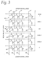
- FIG. 3 illustrates the circuitry of the photo detector array 26, which is formed by a matrix of detector elements 40.
- the detector elements 40 are arranged on an amorphous silicon wafer in a conventional two-dimensional array of m columns and n rows, where m and n are integers.
- a typical high resolution X ray detector is a square array of 1,000 to 4,000 rows and columns of elements.
- the example of Figure 2 has 1280 rows and 1365 columns.
- Each detector element 40 includes a photo diode 42 and a thin film transistor 44.
- the photo diodes 42 are fabricated from a large wafer area ensuring that the photo diode will intercept a sizeable portion of the light produced by the scintillator 24.
- Each photo diode 42 also has a relatively large capacitance that allows it to store electrical charge which is affected by the photon excitation.
- the cathode of the photo diodes 42 in each column of the array is connected by the source-drain conduction path of the associated transistor 44 to a common column signal line (47 or 49) for the column.
- the anodes of the diodes in each row are connected in common to a source of a negative bias voltage (-v).
- the gate electrodes of the transistors 44 in each row are connected to a common row select line 46.
- the row select lines are coupled to the detector controller 27 and the column signal lines are connected to the image processor 28.
- each column of photo detector elements 40 is divided in half with the upper group of photo elements being connected to upper sense lines 47 and the lower group of detector elements being connected to lower sense lines 49.
- the upper group includes rows R1-R640 and the lower group includes rows R641-R1280.
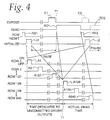
- the first four lines are on a time frame different from the rest of the lines.
- controller 36 takes the initiative to apply the row reset signal RS1, release it, and initialize the drive modules and advance the "1" bit in the shift register of the drive modules as if read out of the detector had begun.
- 128 outputs OP are activated corresponding to the 128 uncommitted outputs adjacent edge E1 of detector 22.
- the first 128 rows of detector 22, R1-R128, are activated by generating pulses A1 - A128, which are transmitted to the row select lines shown in Figure 3.
- Rows R1-R128 include unneeded data because they lie outside the field of view.
- Initialize signal I1 indicates that the initialize period begins with the activation of the first uncommitted drive module output adjacent edge E1 and continues through the activation of row R1 through the activation of row R128.
- the detector pauses, waiting for the "read" command RD1 (shown in Figure 4 as a composite of several more detailed signals) from the system controller 36.
- the detector resumes operating the driver modules as it had before, only the next driver output to be operated will be part of the desired field of view (i.e., row 129 in this example).
- controller 36 When readout is complete, controller 36 again applies a row reset signal RS2 for a short while, initializes the drive modules, and again begins to operate the uncommitted drive outputs adjacent edge E1 as if read out had begun, pausing before the first output in the desired field of view until the "read" command RD2 is received from controller 36.
- the time period indicated by the "read" signal RD1 illustrates the time period required to scan the part of the detector that contains image data of interest (i.e., rows R129-R1152), regardless of the number of uncommitted driver outputs, or number of scan lines outside the field of view requiring scrubbing.
- the initialize period, indicated by the initialize signal I1 is the time during which the uncommitted driver module outputs adjacent edge E1 are activated and the time during which the driver module outputs adjacent edge E1 including unneeded data outside the field of view are activated.
- Initialize period I1 occurs prior to or during exposure period E1, and initialize period I2 occurs after a "read" period (i.e., RD1) during an exposure period E2.
- Exposure period E2 is shown as a phantom exposure in order to illustrate how exposure period E2 overlaps with initialize period I2.
- Period I2 is followed by the beginning of a second phantom read period RD2. If an exposure does not immediately follow the conclusion of a read period RD1, system controller 36 executes the reset and initialize periods as indicated and simply pauses (also shown in phantom), waiting for the next exposure.
- rows R641-R1280 is the same as the above-described operation for rows R1-R640, except that rows R641-R1280 are activated in direction D2 ( Figure 2).
Landscapes
- Health & Medical Sciences (AREA)
- Life Sciences & Earth Sciences (AREA)
- Engineering & Computer Science (AREA)
- Medical Informatics (AREA)
- Physics & Mathematics (AREA)
- General Health & Medical Sciences (AREA)
- Molecular Biology (AREA)
- High Energy & Nuclear Physics (AREA)
- Heart & Thoracic Surgery (AREA)
- Public Health (AREA)
- Optics & Photonics (AREA)
- Pathology (AREA)
- Radiology & Medical Imaging (AREA)
- Biomedical Technology (AREA)
- Biophysics (AREA)
- Veterinary Medicine (AREA)
- Surgery (AREA)
- Animal Behavior & Ethology (AREA)
- Nuclear Medicine, Radiotherapy & Molecular Imaging (AREA)
- Multimedia (AREA)
- Signal Processing (AREA)
- General Physics & Mathematics (AREA)
- Spectroscopy & Molecular Physics (AREA)
- Toxicology (AREA)
- Mathematical Physics (AREA)
- Human Computer Interaction (AREA)
- Apparatus For Radiation Diagnosis (AREA)
- Measurement Of Radiation (AREA)
- Transforming Light Signals Into Electric Signals (AREA)
- Closed-Circuit Television Systems (AREA)
Abstract
Description
- This invention relates to x-ray systems employing a solid state detector and more particularly relates to such systems in which data of interest occupies less than all elements of the detector.
- Experience has shown that a modular design approach to x-ray detector control helps reduce the time to market. By using this approach, a common set of modular electronics may support three different detectors, such as a 41 cm square Radiographic detector, a 20 cm square Cardiographic detector, both consisting of square 0.2 mm pixels; and a Mammographic detector that is 23 cm X 19.2 cm, consisting of square 0.1 mm pixels. The support electronics, consisting of drive modules to control the detector's field effect transistor (FET) switches and sense modules to read and convert the signal, may be 256 channel subsystems, designed to support detectors with 0.2 mm pixel pitch. Both the Cardiographic and Radiographic detectors may require an exact integer number of modules. The Mammographic detector, however, is different in a number of respects. It is rectangular and the pixel pitch is 0.1 mm. The smaller pitch is accommodated by sensing alternate channels from opposite sides, reducing the effective pitch of the sense electronics from 0.2 mm to 0.1 mm. The drive modules are similarly attached, although from two sets of (alternating) contacts that are on the same side in order to allow patient access to one edge of the detector. At first glance it would appear that both a non-integer number of drive and sense modules would be required. However, an exact multiple of 256 sense channels is required across the 19.2 cm dimension. The drive modules however would support 2560 channels, while only 2304 are required. An even number of modules may be required due to the manner in which the pitch mismatch between the detector and the module is managed, even though the requirements suggest that the problem could be solved with 9 (rather than 10) drive modules. This means that 128 drive channels are not committed to the detector on each end.
- Given that the drive module consists of a custom Application Specific Integrated Circuit (ASIC), designed to function like a serial shift register with high voltage outputs, at least the first 128 uncommitted driver channels will require consideration during read out of the detector. The last 128 channels can be ignored due to the operation of module reset, which allows asynchronous reset of the shift register. One current FFDM x-ray detector is operated as if it consisted of 2432 scan lines. That is, the first 128 uncommitted drive channels are operated just like the following 2304 drive channels that are attached to detector scan lines, with the exception that the corresponding "image" data is not transferred out of the detector. This is because this data does not contain any X-Ray exposure information. However, operating the drive electronics in this manner imposes more than 5% of useless overhead (time).
- Similarly, when smaller fields of view than the actual size of the detector are required, the scan lines not in the field of view will require scrubbing (that is the detector is read to restore the charge for each pixel, but the data is discarded). If the FETs are not scrubbed or read for long periods of time, the threshold voltage shifts (in an irreversible fashion) and the FETs no longer provide the necessary isolation when they are off, or conversely, may not provide low enough impedance when on to allow the pixel charge to be quickly and thoroughly restored, resulting in erroneous signal conversion in either case. If the scan lines outside the field of view are scrubbed in a fashion similar to the uncommitted drive channels of the FFDM detector, no advantage in read out time will be enjoyed by defining a smaller field of view on a larger detector. In order to support higher acquisition rates, a smaller detector would need to be substituted, which is a disadvantage in comparison to present Image Intensifier based systems which can easily switch between different field sizes. Conversely, a very complex readout algorithm shared between the detector and the X-Ray system could be defined which would be prone to error, corrupting the image acquisition in the process.
- U.S. Patent No. 4,996,413 discloses a split image x-ray detector that is read from the middle to the outside. Although this reading technique was an improvement in the art, subsequent research has shown that it is desirable for at least some applications to read the detector from the outside toward the middle. The present invention provides a technique for reading detectors that is an improvement on the teaching of U.S. Patent No. 4,996,413.
- The present invention addresses the foregoing problems and provides a solution.
- The preferred embodiment of the present invention is useful in an x-ray system for reading data from a detector array comprising detector elements arranged in rows and columns. The rows typically comprise a first plurality of rows including unneeded data and a second plurality of rows including data of interest. In such an environment, apparatus for coordinating the activation of the detector elements in relation to the exposure of a patient to x-rays to improve the efficiency with which the data of interest is read preferably comprises an x-ray tube generating x-rays. An exposure control is arranged to activate the x-ray tube to expose the detector to x-rays during a predetermined first time period. A detector controller is arranged to activate the first plurality of rows at least partially before or during the first time period and to activate the second plurality of rows after the first time period. An image processor is arranged to read the data in the second plurality of rows after the first time period.
- Another embodiment includes a method analogous to the above-described apparatus.
- By using the foregoing techniques, the overhead associated with scrubbing or partial read out of solid-state x-ray detectors can be substantially reduced.
- Embodiments of the invention will now be described, by way of example, with reference to the accompanying drawings, in which:
- Figure 1 is a schematic block diagram of a preferred form of x-ray system embodying the present invention and employing a solid-state detector.
- Figure 2 is a schematic top plan view of the detector shown in Figure 1, together with exemplary drive and sense circuits.
- Figure 3 is a schematic, fragmentary view showing addition details of the detector shown in Figure 2.
- Figure 4 is a timing diagram illustrating a preferred mode of operation of the apparatus show in Figure 1.
-
- In some present x-ray systems, read out of any of the detectors is initiated by the X-Ray system and is accomplished by releasing driver reset, initializing the drive ASIC, and alternating between enabling (the output of the shift register storing a "1") and clocking (the shift register to advance the stored "1" to the next bit). Uncommitted driver outputs are not operated any differently than driver outputs attached to detector scan lines. The operation of the uncommitted driver outputs take time that has no benefit and may impede faster acquisition rates that different applications may demand. A similar statement could be made about scan lines outside the field of view.
- By using the preferred embodiment of the present invention, a different readout sequence is adopted by the detector. Specifically, the operation of uncommitted drive outputs or scan lines outside the field of view can be accomplished during the exposure time, masking the time required to do so in a manner that is transparent to the rest of the system.
- Referring to Figure 1, an
X-ray system 14 made in accordance with the preferred embodiment includes anX ray tube 15 which, when excited by apower supply 16, emits anX-ray beam 17. As illustrated, the X-ray beam is directed toward apatient 18 lying on an X-ray transmissive table 20. The portion of the beam which is transmitted through the table and the patient impinges upon an X-ray detector designated 22. TheX-ray detector 22 comprises ascintillator 24 that converts the X-ray photons to lower energy photons in the visible spectrum. Contiguous with thescintillator 24 is aphoto detector array 26, which converts the light photons into an electrical signal. Adetector controller 27 contains electronics for operating the detector array to acquire an image and to read out the signal from each photo detector element. - The output signal from the
photo detector array 26 is coupled to animage processor 28 that includes circuitry for processing and enhancing the X ray image signal. The processed image then is displayed on a video monitor 32 and may be archived in animage storage device 30. Theimage processor 28 additionally produces a brightness control signal which is applied to anexposure control circuit 34 to regulate thepower supply 16 and thereby the X-ray exposure. - The overall operation of the
x-ray apparatus 14 is governed by asystem controller 36 that receives commands from the X-ray technician via anoperator interface panel 38. Throughpanel 38, the operator can control the portion of the detector within a field of view by well-known means. - Figure 2 depicts
detector 22 in order to illustrate the operation of both uncommitted driver outputs as well as scan lines outside a desired field of view.Detector 22 defines edges E1-E4 and a midlineM. Detector controller 27 includes drive modules 61-66. Each drive module has 256 outputs OP for a total of 1536 outputs. However, along edge E3,detector 22 has only 1280 elements. As a result, 256 of outputs OP are uncommitted to the detector. 128 of the uncommitted outputs are adjacent edge E1, and 128 of the uncommitted outputs are adjacent edge E2. Due to modularity, six drive modules 61-66, capable of driving a total of 1536 scan lines, are required to operate a detector consisting of 1280 scan lines. Because the detector is split in the middle, and because a drive module can only be operated in one direction, the total number of drive modules required is an even number, with half above and half below midline M. No drive module can straddle the split. Thus, each drive module is coupled exclusively to one part of the split. Each drive module operates like a shift register.Detector 22 includes rows R1-R1280 and columns C1-C1365. -
Image processor 28 includes sense circuits 71-76. Each sense circuit has 256 inputs or sense lines IP for a total of 1536 inputs. However, along edge E1,detector 22 has only 1365 elements. As a result, 171 inputs are uncommitted todetector 22.Detector 22 is split across the sense lines in the middle along a midline M. Because of the split in the sense lines, an additional bank of sense electronics (not shown for the sake of simplicity) is located adjacent edge E2 to accomplish readout of the detector. Due to the effects of charge retention,detector 22 is read from the outside in (i.e., in the directions of arrows D1 and D2). Charge retention offsets have higher variation at the beginning of scan (due to the temporal factor in charge retention current decay during what may be a variable expose, or time between frames) and are more predictable at the end. Reading the center (i.e., adjacent line M) last means that charge retention will less likely corrupt the image. - During use, an operator enters a field of view through
interface 38. In the example of Figure 2, the field of view in 1024 by 1024 pixels or elements ofdetector 22. Thus, there are 256 rows of detector elements with unneeded data outside the field of view. There are 128 rows outside the field of view adjacent edge E1 and 128 rows outside the field of view adjacent edge E2. - FIG. 3 illustrates the circuitry of the
photo detector array 26, which is formed by a matrix ofdetector elements 40. Thedetector elements 40 are arranged on an amorphous silicon wafer in a conventional two-dimensional array of m columns and n rows, where m and n are integers. For example, a typical high resolution X ray detector is a square array of 1,000 to 4,000 rows and columns of elements. The example of Figure 2 has 1280 rows and 1365 columns. - Each
detector element 40 includes aphoto diode 42 and athin film transistor 44. Thephoto diodes 42 are fabricated from a large wafer area ensuring that the photo diode will intercept a sizeable portion of the light produced by thescintillator 24. Eachphoto diode 42 also has a relatively large capacitance that allows it to store electrical charge which is affected by the photon excitation. - The cathode of the
photo diodes 42 in each column of the array is connected by the source-drain conduction path of the associatedtransistor 44 to a common column signal line (47 or 49) for the column. The anodes of the diodes in each row are connected in common to a source of a negative bias voltage (-v). The gate electrodes of thetransistors 44 in each row are connected to a common rowselect line 46. The row select lines are coupled to thedetector controller 27 and the column signal lines are connected to theimage processor 28. - As shown in Figure 3, each column of
photo detector elements 40 is divided in half with the upper group of photo elements being connected to upper sense lines 47 and the lower group of detector elements being connected to lower sense lines 49. The upper group includes rows R1-R640 and the lower group includes rows R641-R1280. With this photo detector array structure, when the detector elements are to be read out individually, a row in the upper half and a row in the lower half of the array are read simultaneously. The upper group is read in the direction D1 while the lower group is read in direction D2. - Referring to Figure 4, the first four lines (i.e., the lines with signals E1, RD1, RS1 and I1) are on a time frame different from the rest of the lines. Shortly after power is applied to the detector,
controller 36 takes the initiative to apply the row reset signal RS1, release it, and initialize the drive modules and advance the "1" bit in the shift register of the drive modules as if read out of the detector had begun. In the example of Figure 2, 128 outputs OP are activated corresponding to the 128 uncommitted outputs adjacent edge E1 ofdetector 22. After the 128 uncommitted outputs are activated, the first 128 rows ofdetector 22, R1-R128, are activated by generating pulses A1 - A128, which are transmitted to the row select lines shown in Figure 3. Rows R1-R128 include unneeded data because they lie outside the field of view. Initialize signal I1 indicates that the initialize period begins with the activation of the first uncommitted drive module output adjacent edge E1 and continues through the activation of row R1 through the activation of row R128. When the last row outside the field of view (i.e., row R128) is reached, the detector pauses, waiting for the "read" command RD1 (shown in Figure 4 as a composite of several more detailed signals) from thesystem controller 36. When the read command RD1 is received, the detector resumes operating the driver modules as it had before, only the next driver output to be operated will be part of the desired field of view (i.e.,row 129 in this example). When readout is complete,controller 36 again applies a row reset signal RS2 for a short while, initializes the drive modules, and again begins to operate the uncommitted drive outputs adjacent edge E1 as if read out had begun, pausing before the first output in the desired field of view until the "read" command RD2 is received fromcontroller 36. - Still referring to Figure 4, the time period indicated by the "read" signal RD1 illustrates the time period required to scan the part of the detector that contains image data of interest (i.e., rows R129-R1152), regardless of the number of uncommitted driver outputs, or number of scan lines outside the field of view requiring scrubbing. The initialize period, indicated by the initialize signal I1, is the time during which the uncommitted driver module outputs adjacent edge E1 are activated and the time during which the driver module outputs adjacent edge E1 including unneeded data outside the field of view are activated.
- Two initialize periods are depicted. Initialize period I1 occurs prior to or during exposure period E1, and initialize period I2 occurs after a "read" period (i.e., RD1) during an exposure period E2. Exposure period E2 is shown as a phantom exposure in order to illustrate how exposure period E2 overlaps with initialize period I2. Period I2 is followed by the beginning of a second phantom read period RD2. If an exposure does not immediately follow the conclusion of a read period RD1,
system controller 36 executes the reset and initialize periods as indicated and simply pauses (also shown in phantom), waiting for the next exposure. - The operation for rows R641-R1280 is the same as the above-described operation for rows R1-R640, except that rows R641-R1280 are activated in direction D2 (Figure 2).
- For completeness, various aspects of the invention are set out in the following numbered clauses:
- 1. In an x-ray system (14) for reading data from a detector array (22)
comprising a predetermined number of detector elements (40) arranged in
rows (R1-R1280) and columns (C1-C1365), said rows comprising a first
plurality of rows including unneeded data (R1-R128) and a second plurality of
rows including data of interest (R129-R1152), apparatus for coordinating the
activation of the detector elements in relation to the exposure of a patient to
x-rays to improve the efficiency with which the data of interest is read
comprising:
- an x-ray tube (15) generating x-rays;
- an exposure control (34) arranged to activate the x-ray tube to expose the detector to x-rays during a predetermined first time period (E1);
- a detector controller (27) arranged to activate the first plurality of rows at least partially before or during the first time period (11) and to activate the second plurality of rows after the first time period (R1); and
- an image processor (28) arranged to read the data in said second plurality of rows after the first time period.
- 2. Apparatus, as claimed in
clause 1, wherein the system comprises an operator interface (38) arranged to select a field of view in the detector and wherein the first plurality of rows are outside the selected field of view. - 3. Apparatus, as claimed in
clause 1, wherein the detector elements define a first edge (E1), a second edge (E2) and a midline (M) between the first edge and the second edge, wherein the first plurality of rows comprises a first group adjacent the first edge (R1-R128) and a second group adjacent the second edge (R1152-R1280) and wherein the first group is activated in a direction from the first edge to the midline while the second group is activated in a direction from the second edge to the midline. - 4. Apparatus, as claimed in
clause 1, wherein said rows comprise row select lines (46), wherein said columns comprise column signal lines (47, 49), wherein the detector elements (40) each comprise a photodiode (42) and a transistor (44) and wherein the transistor connects the photodiode between a row select line and a column signal line, and wherein detector controller activates each row by switching the transistor in the row to conducting states. - 5. Apparatus, as clauimed in clause 4, wherein the image processor is coupled to the column signal lines.
- 6. Apparatus, as claimed in clause 4, wherein the detector elements define a first edge, a second edge and a midline between the first edge and the second edge, and wherein the detector elements are split into a first section (R1-R640) in which the column signal lines are located adjacent the first edge and a second section (R641-R1280)in which the column signal lines are located adjacent the second edge.
- 7. Apparatus, as claimed in clause 6, wherein the rows of the first section of detector elements are activated from the first edge in a direction toward the midline (D1) while the rows of the second section are activated from the second edge in a direction toward the midline (D2).
- 8. Apparatus, as claimed in clause 7, wherein each photo diode (42) comprises a capacitance allowing charge storage.
- 9. Apparatus, as claimed in clause 7, wherein the detector controller comprises a plurality of drive modules (61-66) and wherein each drive module is coupled exclusively to the first section or the second section.
- 10. Apparatus, as claimed in
clause 1, wherein the detector controller comprises a plurality of drive modules having a first plurality of outputs unneeded for activation of the detector elements and a second plurality of outputs needed for activation of the detector elements, and wherein the detector controller activates the first plurality of outputs at least partially before or during the first time period and activates the second plurality of outputs after the first time period. - 11. In an x-ray system (14) for reading data from a detector array (22)
comprising a predetermined number of detector elements (40) arranged in
rows (R1-R1280) and columns (C1-C1365), said rows comprising a first
plurality of rows including unneeded data (R1-R128) and a second plurality of
rows including data of interest (R129-R1152), a method of coordinating the
activation of the detector elements in relation to the exposure of a patient to
x-rays to improve the efficiency with which the data of interest is read
comprising:
- generating x-rays;
- exposing the detector to x-rays during a predetermined first time period;
- activating the first plurality of rows at least partially before or during the first time period and activating the second plurality of rows after the first time period; and
- reading the data in said second plurality of rows after the first time period.
- 12. A method, as claimed in
clause 11, and further comprising selecting a field of view in the detector and wherein the first plurality of rows is outside the selected field of view. - 13. A method, as claimed in
clause 11, wherein the detector elements define a first edge (E1), a second edge (E2) and a midline (M) between the first edge and the second edge, wherein the first plurality of rows comprises a first group adjacent the first edge (R1-R128) and a second group adjacent the second edge (R1152-R1280) and wherein said activating comprises activating the first plurality of rows in a direction from the first edge to the midline while activating the second group in a direction from the second edge to the midline. - 14. A method, as claimed in
clause 11, wherein said rows comprise row select lines (46), wherein said columns comprise column signal lines (47, 49), wherein the detector elements (40) each comprise a photodiode (42) and a transistor (44) and wherein the transistor connects the photodiode between a row select line and a column signal line, and wherein said activating comprises switching the transistors in the row to conducting states. - 15. A method, as claimed in
clause 14, wherein said reading comprises coupling the photodiode to the column signal lines. - 16. A method, as claimed in
clause 14, wherein the detector elements define a first edge, a second edge and a midline between the first edge and the second edge, and wherein the detector elements are split into a first section in which the column signal lines are located adjacent the first edge and a second section in which the column signal lines are located adjacent the second edge. - 17. A method, as claimed in
clause 16, wherein said activating comprises activating the rows of the first section of detector elements from the first edge in a direction toward the midline while activating the rows of the second section from the second edge in a direction toward the midline. - 18. A method, as claimed in
clause 17, and further comprising storing charge in said photodiodes (42). -
Claims (10)
- An x-ray apparatus including means for reading data from a detector array (22) comprising a predetermined number of detector elements (40) arranged in rows (R1-R1280) and columns (C1-C1365), said rows comprising a first plurality of rows including unneeded data (R1-R128) and a second plurality of rows including data of interest (R129-R1152), and means for coordinating the activation of the detector elements in relation to the exposure of a patient to x-rays to improve the efficiency with which the data of interest is read comprising:an x-ray tube (15) generating x-rays;an exposure control (34) arranged to activate the x-ray tube to expose the detector to x-rays during a predetermined first time period (E1);a detector controller (27) arranged to activate the first plurality of rows at least partially before or during the first time period (I1) and to activate the second plurality of rows after the first time period (R1); andan image processor (28) arranged to read the data in said second plurality of rows after the first time period.
- Apparatus, as claimed in claim 1, including an operator interface (38) arranged to select a field of view in the detector and wherein the first plurality of rows are outside the selected field of view.
- Apparatus, as claimed in claim 1, wherein the detector elements define a first edge (E1), a second edge (E2) and a midline (M) between the first edge and the second edge, wherein the first plurality of rows comprises a first group adjacent the first edge (R1-R128) and a second group adjacent the second edge (R1152-R1280) and wherein the first group is activated in a direction from the first edge to the midline while the second group is activated in a direction from the second edge to the midline.
- Apparatus, as claimed in claim 1, wherein said rows comprise row select lines (46), wherein said columns comprise column signal lines (47, 49), wherein the detector elements (40) each comprise a photodiode (42) and a transistor (44) and wherein the transistor connects the photodiode between a row select line and a column signal line, and wherein detector controller activates each row by switching the transistor in the row to conducting states.
- Apparatus, as claimed in claim 4, wherein the detector elements define a first edge, a second edge and a midline between the first edge and the second edge, and wherein the detector elements are split into a first section (R1-R640) in which the column signal lines are located adjacent the first edge and a second section (R641-R1280)in which the column signal lines are located adjacent the second edge.
- Apparatus, as claimed in claim 1, wherein the detector controller comprises a plurality of drive modules having a first plurality of outputs unneeded for activation of the detector elements and a second plurality of outputs needed for activation of the detector elements, and wherein the detector controller activates the first plurality of outputs at least partially before or during the first time period and activates the second plurality of outputs after the first time period.
- An x-ray method including reading data from a detector array (22) comprising a predetermined number of detector elements (40) arranged in rows (R1-R1280) and columns (C1-C1365), said rows comprising a first plurality of rows including unneeded data (R1-R128) and a second plurality of rows including data of interest (R129-R1152), and coordinating the activation of the detector elements in relation to the exposure of a patient to x-rays to improve the efficiency with which the data of interest is read, comprising:generating x-rays;exposing the detector to x-rays during a predetermined first time period;activating the first plurality of rows at least partially before or during the first time period and activating the second plurality of rows after the first time period; andreading the data in said second plurality of rows after the first time period.
- A method, as claimed in claim 7, and further comprising selecting a field of view in the detector and wherein the first plurality of rows is outside the selected field of view.
- A method, as claimed in claim 7, wherein the detector elements define a first edge (E1), a second edge (E2) and a midline (M) between the first edge and the second edge, wherein the first plurality of rows comprises a first group adjacent the first edge (R1-R128) and a second group adjacent the second edge (R1152-R1280) and wherein said activating comprises activating the first plurality of rows in a direction from the first edge to the midline while activating the second group in a direction from the second edge to the midline.
- A method, as claimed in claim 7, wherein said rows comprise row select lines (46), wherein said columns comprise column signal lines (47, 49), wherein the detector elements (40) each comprise a photodiode (42) and a transistor (44) and wherein the transistor connects the photodiode between a row select line and a column signal line, and wherein said activating comprises switching the transistors in the row to conducting states.
Applications Claiming Priority (2)
| Application Number | Priority Date | Filing Date | Title |
|---|---|---|---|
| US681300 | 2001-03-15 | ||
| US09/681,300 US6404852B1 (en) | 2001-03-15 | 2001-03-15 | Overhead reduction due to scrubbing or partial readout of x-ray detectors |
Publications (2)
| Publication Number | Publication Date |
|---|---|
| EP1248456A2 true EP1248456A2 (en) | 2002-10-09 |
| EP1248456A3 EP1248456A3 (en) | 2010-02-24 |
Family
ID=24734686
Family Applications (1)
| Application Number | Title | Priority Date | Filing Date |
|---|---|---|---|
| EP02251786A Withdrawn EP1248456A3 (en) | 2001-03-15 | 2002-03-13 | Partial readout of x-ray detectors |
Country Status (3)
| Country | Link |
|---|---|
| US (1) | US6404852B1 (en) |
| EP (1) | EP1248456A3 (en) |
| JP (1) | JP4204239B2 (en) |
Families Citing this family (20)
| Publication number | Priority date | Publication date | Assignee | Title |
|---|---|---|---|---|
| US6031892A (en) * | 1989-12-05 | 2000-02-29 | University Of Massachusetts Medical Center | System for quantitative radiographic imaging |
| EP2101495B1 (en) * | 1996-02-28 | 2012-12-26 | Panasonic Corporation | High-resolution optical disk for recording stereoscopic video, optical disk reproducing device and optical disk recording device |
| US6931098B2 (en) * | 2002-03-08 | 2005-08-16 | Ge Medical Systems Global Technology Company, Llc | Method and system for dual or multiple energy imaging |
| JP3647440B2 (en) * | 2002-05-28 | 2005-05-11 | キヤノン株式会社 | X-ray equipment |
| US6718010B2 (en) * | 2002-06-11 | 2004-04-06 | Ge Medical Systems Global Technology Company, Llc | Method and apparatus for acquiring a series of images utilizing a solid state detector with alternating scan lines |
| US7248671B2 (en) * | 2002-06-26 | 2007-07-24 | Kabushiki Kaisha Toshiba | X-ray diagnosis apparatus |
| JP4570614B2 (en) * | 2003-03-24 | 2010-10-27 | カルテンバッハ ウント ホイクト ゲゼルシャフト ミット ベシュレンクテル ハフツング | X-ray system with electronic sensor |
| JP2005109269A (en) * | 2003-09-30 | 2005-04-21 | Hitachi Ltd | Semiconductor radiation detector and semiconductor radiation imager |
| US7119341B2 (en) * | 2003-12-08 | 2006-10-10 | General Electric Company | Split scan line and combined data line x-ray detectors |
| US20050147203A1 (en) * | 2003-12-31 | 2005-07-07 | Ross William R. | Reading imaging data |
| DE102004052613B4 (en) * | 2004-10-29 | 2016-03-03 | Siemens Aktiengesellschaft | Mammography X-ray machine with a digital solid-state flat detector |
| JP2007144064A (en) * | 2005-11-30 | 2007-06-14 | Shimadzu Corp | Imaging sensor and imaging unit using the same |
| KR100987857B1 (en) * | 2006-02-23 | 2010-10-13 | 가부시키가이샤 시마즈세이사쿠쇼 | Radiation image pick-up device and radiation detecting signal processing method |
| JP2008098391A (en) * | 2006-10-12 | 2008-04-24 | Fujifilm Corp | Radiation image detector |
| US7601962B2 (en) | 2007-01-12 | 2009-10-13 | General Electric Company | Systems and methods for reading data |
| JP5361152B2 (en) * | 2007-07-09 | 2013-12-04 | キヤノン株式会社 | Imaging control apparatus and control method therefor, imaging apparatus, and program |
| KR101599028B1 (en) * | 2009-07-23 | 2016-03-03 | 삼성전자주식회사 | - X-ray Apparatus for generating X-ray image for reducing scatter and method thereof |
| KR101829777B1 (en) * | 2011-03-09 | 2018-02-20 | 삼성디스플레이 주식회사 | Optical sensor |
| JP5627748B2 (en) * | 2013-09-03 | 2014-11-19 | キヤノン株式会社 | Imaging control apparatus and control method therefor, imaging apparatus, and program |
| JP2018014555A (en) * | 2016-07-19 | 2018-01-25 | 東芝電子管デバイス株式会社 | Radiation detection device and radiographic imaging device |
Citations (2)
| Publication number | Priority date | Publication date | Assignee | Title |
|---|---|---|---|---|
| US4996413A (en) | 1990-02-27 | 1991-02-26 | General Electric Company | Apparatus and method for reading data from an image detector |
| EP0792062A2 (en) | 1996-02-22 | 1997-08-27 | Canon Kabushiki Kaisha | Photoelectric conversion device and driving method therefor |
Family Cites Families (3)
| Publication number | Priority date | Publication date | Assignee | Title |
|---|---|---|---|---|
| US5668375A (en) * | 1996-08-26 | 1997-09-16 | General Electric Company | Fast scan reset for a large area x-ray detector |
| US5970115A (en) * | 1996-11-29 | 1999-10-19 | Varian Medical Systems, Inc. | Multiple mode digital X-ray imaging system |
| WO1999030485A2 (en) * | 1997-12-10 | 1999-06-17 | Koninklijke Philips Electronics N.V. | X-ray examination apparatus |
-
2001
- 2001-03-15 US US09/681,300 patent/US6404852B1/en not_active Expired - Lifetime
-
2002
- 2002-03-13 EP EP02251786A patent/EP1248456A3/en not_active Withdrawn
- 2002-03-15 JP JP2002071535A patent/JP4204239B2/en not_active Expired - Fee Related
Patent Citations (2)
| Publication number | Priority date | Publication date | Assignee | Title |
|---|---|---|---|---|
| US4996413A (en) | 1990-02-27 | 1991-02-26 | General Electric Company | Apparatus and method for reading data from an image detector |
| EP0792062A2 (en) | 1996-02-22 | 1997-08-27 | Canon Kabushiki Kaisha | Photoelectric conversion device and driving method therefor |
Also Published As
| Publication number | Publication date |
|---|---|
| EP1248456A3 (en) | 2010-02-24 |
| JP4204239B2 (en) | 2009-01-07 |
| JP2002345798A (en) | 2002-12-03 |
| US6404852B1 (en) | 2002-06-11 |
Similar Documents
| Publication | Publication Date | Title |
|---|---|---|
| US6404852B1 (en) | Overhead reduction due to scrubbing or partial readout of x-ray detectors | |
| US7491960B2 (en) | Radiographic apparatus and control method therefor | |
| EP0444869B1 (en) | Apparatus and method for detecting images | |
| US7514663B2 (en) | Imaging apparatus having a read out circuit unit with dual readout operation and method of improving a frame rate | |
| US7381938B2 (en) | Photoelectric converter and x-ray image pick-up device | |
| US7154099B2 (en) | Radiation image pick-up device and radiation image pick-up method | |
| US7109492B2 (en) | Radiographic apparatus | |
| US6818899B2 (en) | Radiographic image pickup apparatus and method of driving the apparatus | |
| US20120006993A1 (en) | Solid-state imaging apparatus and imaging system | |
| JP4652074B2 (en) | Method and system for improved data collection using a solid-state digital X-ray detector | |
| EP3275176B1 (en) | Apparatus and method using a dual gate tft structure | |
| WO2004073068A1 (en) | Radiation image pickup device | |
| US7119341B2 (en) | Split scan line and combined data line x-ray detectors | |
| US6718010B2 (en) | Method and apparatus for acquiring a series of images utilizing a solid state detector with alternating scan lines | |
| CN103067670A (en) | Image pickup unit and image pickup display system | |
| US8822939B2 (en) | Matrix substrate, detection device, detection system, and method for driving detection device | |
| WO2013180077A1 (en) | Radiographic imaging equipment and radiation detector | |
| JPH0784055A (en) | Radiation two-dimensional detector | |
| JP3984676B2 (en) | Photoelectric conversion device and system having the device | |
| US20120105665A1 (en) | Digital image pickup apparatus, radiation imaging apparatus, and radiation imaging system | |
| CN109561874B (en) | Solid-state imaging device, radiation imaging system, and solid-state imaging device control method | |
| US6901134B2 (en) | Arrangement comprising electrical elements | |
| JP2023064459A (en) | Radiation imaging apparatus, radiation imaging system, and method for controlling radiation imaging apparatus | |
| JP2013069864A (en) | Detector and detection system | |
| JP2002148345A (en) | Radiation imaging device, method for setting its sensor bias and radiation imaging system |
Legal Events
| Date | Code | Title | Description |
|---|---|---|---|
| PUAI | Public reference made under article 153(3) epc to a published international application that has entered the european phase |
Free format text: ORIGINAL CODE: 0009012 |
|
| AK | Designated contracting states |
Kind code of ref document: A2 Designated state(s): AT BE CH CY DE DK ES FI FR GB GR IE IT LI LU MC NL PT SE TR |
|
| AX | Request for extension of the european patent |
Free format text: AL;LT;LV;MK;RO;SI |
|
| PUAL | Search report despatched |
Free format text: ORIGINAL CODE: 0009013 |
|
| AK | Designated contracting states |
Kind code of ref document: A3 Designated state(s): AT BE CH CY DE DK ES FI FR GB GR IE IT LI LU MC NL PT SE TR |
|
| AX | Request for extension of the european patent |
Extension state: AL LT LV MK RO SI |
|
| 17P | Request for examination filed |
Effective date: 20100824 |
|
| 17Q | First examination report despatched |
Effective date: 20100917 |
|
| AKX | Designation fees paid |
Designated state(s): DE FR |
|
| GRAP | Despatch of communication of intention to grant a patent |
Free format text: ORIGINAL CODE: EPIDOSNIGR1 |
|
| RIC1 | Information provided on ipc code assigned before grant |
Ipc: H05G 1/30 20060101ALI20180205BHEP Ipc: G01T 1/203 20060101ALI20180205BHEP Ipc: H04N 5/32 20060101ALI20180205BHEP Ipc: A61B 6/00 20060101AFI20180205BHEP Ipc: H04N 5/345 20110101ALI20180205BHEP |
|
| INTG | Intention to grant announced |
Effective date: 20180227 |
|
| STAA | Information on the status of an ep patent application or granted ep patent |
Free format text: STATUS: THE APPLICATION IS DEEMED TO BE WITHDRAWN |
|
| 18D | Application deemed to be withdrawn |
Effective date: 20180710 |
|
| RIC1 | Information provided on ipc code assigned before grant |
Ipc: G01T 1/203 20060101ALI20180205BHEP Ipc: H04N 5/345 20110101ALI20180205BHEP Ipc: H05G 1/30 20060101ALI20180205BHEP Ipc: H04N 5/32 20060101ALI20180205BHEP Ipc: A61B 6/00 20060101AFI20180205BHEP |