EP1249842A1 - Method for programming nonvolatile memory cells with program and verify algorithm using a staircase voltage with varying step amplitude - Google Patents
Method for programming nonvolatile memory cells with program and verify algorithm using a staircase voltage with varying step amplitude Download PDFInfo
- Publication number
- EP1249842A1 EP1249842A1 EP01830247A EP01830247A EP1249842A1 EP 1249842 A1 EP1249842 A1 EP 1249842A1 EP 01830247 A EP01830247 A EP 01830247A EP 01830247 A EP01830247 A EP 01830247A EP 1249842 A1 EP1249842 A1 EP 1249842A1
- Authority
- EP
- European Patent Office
- Prior art keywords
- programming
- pulse
- memory cell
- voltage
- amplitude
- Prior art date
- Legal status (The legal status is an assumption and is not a legal conclusion. Google has not performed a legal analysis and makes no representation as to the accuracy of the status listed.)
- Granted
Links
Images


Classifications
-
- G—PHYSICS
- G11—INFORMATION STORAGE
- G11C—STATIC STORES
- G11C11/00—Digital stores characterised by the use of particular electric or magnetic storage elements; Storage elements therefor
- G11C11/56—Digital stores characterised by the use of particular electric or magnetic storage elements; Storage elements therefor using storage elements with more than two stable states represented by steps, e.g. of voltage, current, phase, frequency
- G11C11/5621—Digital stores characterised by the use of particular electric or magnetic storage elements; Storage elements therefor using storage elements with more than two stable states represented by steps, e.g. of voltage, current, phase, frequency using charge storage in a floating gate
- G11C11/5628—Programming or writing circuits; Data input circuits
-
- G—PHYSICS
- G11—INFORMATION STORAGE
- G11C—STATIC STORES
- G11C16/00—Erasable programmable read-only memories
- G11C16/02—Erasable programmable read-only memories electrically programmable
- G11C16/06—Auxiliary circuits, e.g. for writing into memory
- G11C16/10—Programming or data input circuits
- G11C16/12—Programming voltage switching circuits
Definitions
- the present invention relates to a method for programming nonvolatile memory cells with a program and verify algorithm in which the amplitude of the programming pulses increases in staircase fashion with a variable slope.
- Programming of a nonvolatile memory cell is normally performed by means of a sequence of programming steps interspersed with verification steps in which the state of the memory cell is verified.
- G. Torelli, P. Lupi "An improved method for programming a word-erasable EEPROM", Alta Frequenza , Vol. LII, n. 6, Nov./Dec. 1983, pp. 487-494.
- a programming voltage is applied to the gate terminal of the memory cell, the amplitude of which is increased by a constant amount at each programming step, and the sequence is continued until the threshold voltage of the memory cell, which was initially at a low value, reaches the desired value.
- Figure 1 shows a graph presented in the above-mentioned paper "Technological and design constraints for multilevel flash memories” and representing the linear relationship existing between the threshold voltage of a memory cell and the programming voltage applied to the gate terminal of the memory cell, when said programming voltage presents a pulsed pattern the amplitude of which increases in staircase fashion.
- the amplitude of the programmed threshold voltage distributions depends upon the variation of the threshold voltage ⁇ V T obtained at each step.
- the programming precision i.e., the maximum difference between the threshold-voltage value actually obtained and the desired nominal value, depends upon ⁇ V T .
- the programming precision depends upon ⁇ V G , i.e., upon the increment of the programming voltage at each programming step.
- Figure 2 is a qualitative representation of the distributions of programmed threshold voltages for multilevel cells with 2-bit per cell, using a technology currently available in which the range of programmable threshold voltages is fixed between 1 V and 6 V. Also represented in Figure 2 are the distributions of threshold voltages that may be obtained in the same voltage range for multilevel cells with 4-bit per cell. Likewise represented in Figure 2, as hatched areas, are the corresponding noise margins.
- the width of the programmed threshold voltage distributions must be reduced by at least a factor of four.
- the US patents US-A-4,357,685 “Method of programming an electrically alterable nonvolatile memory”
- US-A-5,812,457 semiconductor NAND type flash memory with incremental step pulse programming”
- the US patent US-A-5,257,255 “Method for programming programmable devices by utilizing single or multiple pulses varying in pulse width and amplitude” describes a programming method that uses single or multiple pulses having varying amplitude or duration, in which a first train of programming pulses is applied to an electrode of the programmable device and, simultaneously, a second train of programming pulses is applied to a second electrode of the programmable device.
- the purpose of the present invention is to provide a method for programming nonvolatile memory cells with a staircase programming voltage having varying incremental amplitude between adjacent programming steps, the said method being based on a program and verify algorithm that enables a further reduction in the time required for high-precision programming as compared to conventional programming methods.
- a method for programming a memory cell based upon a program and verify algorithm is provided, as defined in Claim 1.
- Figure 3 shows a nonvolatile memory cell 1 to be programmed that forms part of a nonvolatile memory device, in which the gate terminal is designated by 2, the drain terminal by 4, and the source terminal by 6.
- the gate terminal 2 of a memory cell is connected to an array row (not shown) selectable by means of a row decoder (not shown), the drain terminal 4 is connected to an array column (not shown) selectable by means of a column decoder (not shown), whilst the source terminal 6 is connected to a common line (not shown).
- Figure 4a shows the staircase waveform of the amplitude of the programming voltage V G applied to the gate terminal of the memory cell 1 in the first embodiment of the present invention.
- the staircase programming voltage V G is not formed by a series of voltage steps succeeding one another in time, but rather of a series of voltage pulses of progressively increasing amplitude succeeding one another in time, as shown in Figure 4b.
- Figure 4c is instead the plot as a function of time of the voltage V D applied to the drain terminal 4 of the memory cell 1, again in the first embodiment of the present invention.
- the first embodiment of the invention envisages programming of the memory cell 1 in two phases.
- a first phase designated in the figure by F1 to the drain terminal 4 and to the gate terminal 2 of the memory cell 1 to be programmed there is applied a first pair of programming (voltage) pulse trains; namely, one programming pulse train of the pair is applied to the drain terminal 4, and the other to the gate terminal 2.
- the programming pulses applied to the drain terminal 4 ( V D ) have a constant amplitude, for example of between 4 V and 5 V, whereas the programming pulses applied to the gate terminal 2 ( V G ) have an increasing amplitude, in such a way that the voltage difference between one programming pulse and the preceding one, i.e., the voltage increment between adjacent pulses ⁇ V G1 , is constant and has a high value, in particular higher than the precision desired for the programmed threshold voltage, for example a value of between 200 mV and 600 mV.
- the programming pulses applied to the drain terminal 4 ( V D ) again have a constant amplitude, preferably equal to the one in the first phase F1, whereas the programming pulses applied to the gate terminal 2 ( V G ) have an increasing amplitude, in such a way that the voltage difference between one programming pulse and the preceding one, i.e., the voltage increment between adjacent pulses ⁇ V G2 , is again constant but has a value lower than ⁇ V G1 and is of the same order of precision as that desired for the threshold voltage programmed, for example between 50 mV and 100 mV.
- the first programming pulse of the second programming pulse train applied to the gate terminal 2 of the memory cell 1 in the second phase F2 has an amplitude equal to that of the last programming pulse of the first programming pulse train applied to the gate terminal 2 in the first phase F1 increased by a quantity ⁇ V G2 .
- transition from the first phase F1 to the second phase F2 takes place after the threshold voltage V T of the memory cell 1 has exceeded a pre-set reference value V TR1 , appropriately chosen below the value of the threshold voltage at which the memory cell 1 is to be programmed.
- Figures 5a, 5b and 5c are similar to Figures 4a, 4b and 4c and show the plots as a function of time of the programming voltage V G and of the voltage V D respectively applied to the gate terminal 2 and to the drain terminal 4 of the memory cell 1 in the second embodiment of the present invention.
- the second embodiment of the present invention envisages programming of the memory cell 1 in three phases.
- a first pair of programming pulse trains namely, one programming pulse train of the pair is applied to the drain terminal 4, and the other to the gate terminal 2.
- the programming pulses applied to the drain terminal 4 have a constant amplitude, for example preferably equal to the one applied in the phases F1 and F2 of the first embodiment, whereas the programming pulses applied to the gate terminal 2 have an increasing amplitude, in such a way that the voltage difference between one programming pulse and the preceding one, i.e., the voltage increment between adjacent pulses ⁇ V G0 , is constant and has a limited value, for example of the same order as that of the precision desired for the programmed threshold voltage.
- the memory cells with different starting threshold voltages or with different characteristics due to the process spreads are substantially brought back to the same conditions.
- the two subsequent phases are the same as the phases F1 and F2 of the first embodiment, and consequently will not be described again.
- ⁇ V G0 may also be equal to ⁇ V G2
- the first pulse of the second phase (phase F1) has an amplitude equal to that of the last pulse of the first phase (phase F0) increased by a quantity ⁇ V G1 .
- Transition from the first phase F0 to the second phase F1 can take place after a fixed number of pulses, or else after the threshold voltage V T of the memory cell 1 has exceeded an appropriately chosen pre-set reference value V TR0 .
- Transition from the second phase F1 to the third phase F2 takes place in a way identical to what was described for the first embodiment.
- Figures 6a, 6b and 6c are similar to Figures 4a, 4b and 4c and show the plots as a function of time of the programming voltage V G and of the voltage V D respectively applied to the gate terminal 2 and to the drain terminal 4 of the memory cell 1 in a third embodiment of the present invention.
- the third embodiment of the present invention represents one of the possible variants of the second embodiment and differs from the latter in that the first programming pulse train applied to the gate terminal 2 of the memory cell 1, designated in the figure by F3, presents a voltage increment between adjacent pulses greater than the one present in the programming pulse train applied to the gate terminal 2 in the second phase F1.
- the third embodiment envisages that programming of the memory cell 1 takes place always in three phases, but that a phase F1 is used with a voltage increment between adjacent pulses that is intermediate between the initial phase F3, in which said increment is greater, and the end phase F2, in which said increment is smaller.
- the present invention proposes a method in which programming of a memory cell is performed by means of application, to a first terminal of the memory cell, namely the gate terminal in the case of memories programmed by injection of channel hot electrons, of at least two distinct successive trains of voltage pulses having precise characteristics, where each train presents pulses in which the voltage is incremented by a given constant value between one pulse and the next, and the value of this increment is different for the different pulse trains, whilst to a second terminal of the memory cell, namely the drain terminal in the case of memory cells programmed by injection of channel hot electrons, there are applied pulse trains having a substantially constant amplitude simultaneously with the pulse trains applied to the gate terminal which have been described previously.
- Transition from one pulse train to another (with the possible exclusion of the transition from phase F0 to phase F1 in the second embodiment) does not follow any pre-defined procedure, but takes place according to the result of the verify operation, which is performed at each programming step by using appropriate references.
- the gate current I G is an increasing function of V G - V T :
- I G f ( V G - V T )
- a gate voltage V G higher than the initial threshold voltage of the memory cell is applied, such that injection of hot electrons from the channel into the floating gate is triggered.
- the variation in the threshold voltage obtained in a programming step depends upon the initial difference between the voltages V G, applied - V T,initial - V D , where V D is a constant that depends upon the biasing conditions and physical characteristics of the memory cell. More precisely, if the programming pulse had an infinite duration, the variation in the threshold voltage would be equal to the value indicated. On account of the non-complete disappearance of the transient during a programming pulse, the threshold-voltage variation actually obtained is a fraction ⁇ of the initial difference between the voltage V G,applied - V T,initial - V D .
- ⁇ depends only upon the duration of the programming pulse, the biasing voltages, and the physical characteristics of the memory cell. Consequently, if programming pulses having a constant duration are considered, ⁇ is a constant.
- Equation (7) is a discrete-time differential equation of the first order, from which it is found that the steady-state value ( ⁇ V G (1 - ⁇ )/ ⁇ + V D ) is reached with a constant 1/ ⁇ over the number of programming steps.
- the programming voltage increment between adjacent steps is reduced to ⁇ V G2 (with ⁇ V G2 ⁇ ⁇ V G1 ).
- Table I of Figure 7 gives the errors on the threshold voltage variation that is obtained after transition from an increment value ⁇ V G2 to a reduced increment value ⁇ V G1 . More precisely, the table gives the errors found after the first pulse ( n + 1) with reduced ⁇ V G , after the second pulse ( n + 2), after the third pulse ( n + 3), and so forth.
- the threshold voltage variation obtained in the course of the subsequent pulses converges towards the steady-state value (100 mV).
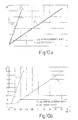
- FIG. 10a and 10b show the plot (10a) of the programming voltage applied to the gate terminal of a memory cell with an increment between adjacent programming steps that assumes two possible values, and the plot (10b) of the corresponding programmed threshold voltage.
- the staircase programming voltages with 200-mV (phase F1) and 50-mV (phase F2) increments between adjacent steps, which indicatively are able to provide the necessary programming precision for 2-bit-per-cell and 4-bit-per-cell storage.
- the temporal duration of a single program and verify step is 2 ⁇ s.
- Programming with varying increments speeds up programming of the individual multilevel cell; for example, it is possible to obtain programming with the precision necessary for 16 levels in the same time that is required for 4 levels with fixed voltage increments.
- the procedure starts with fast programming (F1) until the threshold voltage, controlled in the verify steps, reaches a value close to the one desired ( V TR1 ), and then proceeds with fine programming (F2) until the desired value is reached.
- an appropriate electric quantity (voltage or current) is extracted from the multilevel memory cell and compared with a set of reference values in order to reconstruct the information content of the memory cell in terms of binary information.
- each verify step generally a complete reading of the memory cell is not performed, but simply the electric quantity extracted is compared with a single reference value, which depends upon the threshold voltage value at which the memory cell is to be programmed. To carry out this operation, one of the comparators used for reading can be utilized.
- the comparator used for the verification compares the value of the electric quantity extracted from the memory cell, which is linked to the threshold voltage reached, with:
- the two possible increments between adjacent values are: according to whether the control signal CNT is active or not.
- the complete circuit for generating the programming voltage is formed by a staircase generator block (of the type of the ones referred to above) and possibly by an amplifier, connected in unit-gain configuration, which is capable of fast driving of the parasitic capacitance associated to the array row driving stage, as represented in Figure 12.
Abstract
Description
where the amplitude of the steps is not constant, but rather varies according to different modalities.
- Figure 1 shows a graph representing the linear relationship existing between the threshold voltage of a memory cell and the programming voltage applied to the gate terminal of the memory cell, when the programming voltage presents a staircase waveform;
- Figures 2a and 2b are representations of the programmed threshold voltage distributions for multilevel cells with 2-bit per cell and, respectively, 4-bit per cell, and of the corresponding noise margins;
- Figure 3 is a schematic representation of a nonvolatile memory cell;
- Figure 4a shows, in a simplified and qualitative way, the plot as a function of time of the programming voltage applied to the gate terminal of the memory cell of Figure 1 in a first embodiment of the present invention;
- Figures 4b and 4c are the effective plots as a function of time of the voltages applied to the gate terminal and, respectively, to the drain terminal of the memory cell of Figure 1 in the first embodiment of the present invention;
- Figure 5a shows, in a simplified and qualitative way, the plot as a function of time of the programming voltage applied to the gate terminal of the memory cell of Figure 1 in a second embodiment of the present invention;
- Figures 5b and 5c are the effective plots as a function of time of the voltages applied to the gate terminal and, respectively, to the drain terminal of the memory cell of Figure 1 in the second embodiment of the present invention;
- Figure 6a shows, in a simplified and qualitative way, the plot as a function of time of the programming voltage applied to the gate terminal of the memory cell of Figure 1 in a third embodiment of the present invention;
- Figures 6b and 6c are the effective plots as a function of time of the voltages applied to the gate terminal and, respectively, to the drain terminal of the memory cell of Figure 1 in the third embodiment of the present invention;
- Figures 7, 8 and 9 are tables referring to the programming method according to the present invention;
- Figures 10a and 10b show, respectively, a plot as a function of time of the programming voltage applied to the gate terminal of a memory cell with voltage increment between adjacent steps that assumes two possible values, and a plot as a function of time of the corresponding programmed threshold voltage;
- Figure 11 shows the a switched-capacitor circuit for the generation of a varying incremental staircase voltage; and
- Figure 12 shows the block diagram of a circuit for the generation of the staircase programming voltage with varying increments between adjacent steps.
- a preliminary reference, appropriately chosen lower than the target value, during fast programming; and
- the final reference, once there has been the transition to fine programming.

Claims (14)
- A method for programming a memory cell (1), characterized in that it comprises the step of applying in succession, to a control terminal (2) of said memory cell (1), at least a first and a second programming pulse trains (F1, F2) with pulse amplitude increasing in staircase fashion, in which the amplitude increment between one pulse and next in said first programming pulse train (F1) is greater than the amplitude increment between one pulse and the next in said second programming pulse train (F2).
- The programming method according to Claim 1, characterized in that transition from said first programming pulse train (F1) to said second programming pulse train (F2) is made when said memory cell (1) has a threshold voltage (V T) having a first pre-set relation with a first reference value (V TR1).
- The programming method according to Claim 2, characterized in that said first pre-set relation is defined by the condition that the threshold voltage (V T) of said memory cell (1) exceeds said first reference value (V TR1).
- The programming method according to Claim 2 or Claim 3, characterized in that said first reference value (V TR1) is correlated to the threshold voltage (V T) at which said memory cell (1) is to be programmed.
- The programming method according to Claim 4, characterized in that said first reference value (V TR1) is lower than the threshold voltage (V T) at which said memory cell (1) is to be programmed.
- The programming method according to any of the foregoing claims, characterized in that it further comprises the step of applying, to said control terminal (2) of said memory cell (1) and before said first programming pulse train (F1), a third programming pulse train (F0; F3) with pulse amplitude increasing in staircase fashion.
- The programming method according to Claim 6, characterized in that the amplitude increment between one pulse and the next in said third programming pulse train (F0) is less than the amplitude increment between one pulse and the next in said first programming pulse train (F1).
- The programming method according to Claim 6 or Claim 7, characterized in that the amplitude increment between one pulse and the next in said third programming pulse train (F0) is substantially equal to the amplitude increment between one pulse and the next in said second programming pulse train (F2).
- The programming method according to Claim 6, characterized in that the amplitude increment between one pulse and the next in said third programming pulse train (F3) is greater than the amplitude increment between one pulse and the next in said first programming pulse train (F1).
- The programming method according to any of Claims 6 to 9, characterized in that transition from said third programming pulse train (F0; F3) to said first programming pulse train (F1) is made when said memory cell (1) presents a threshold voltage (V T) having a second pre-set relation with a second reference value (V TR0).
- The programming method according to Claim 10, characterized in that said second pre-set relation is defined by the condition that the threshold voltage (V T) of said memory cell (1) exceeds said second reference value (V TR0).
- The programming method according to any of Claims 6 to 9, characterized in that transition from said third programming pulse train (F0; F3) to said first programming pulse train (F1) is made after a pre-set number of programming pulses.
- The programming method according to any of the foregoing claims, characterized in that it further comprises the step of applying, to a first terminal (4) of said memory cell (1) and simultaneously to each one of said programming pulse trains (F0, F1, F2, F3) applied to said control terminal (2), a respective programming pulse trains (V D) with constant pulse amplitude.
- The programming method according to Claim 13, characterized in that said programming pulse trains (V D) applied to said first terminal (4) of said memory cell (1) have pulse amplitudes substantially equal to one another.
Priority Applications (4)
| Application Number | Priority Date | Filing Date | Title |
|---|---|---|---|
| EP01830247A EP1249842B1 (en) | 2001-04-10 | 2001-04-10 | Method for programming nonvolatile memory cells with program and verify algorithm using a staircase voltage with varying step amplitude |
| DE60139670T DE60139670D1 (en) | 2001-04-10 | 2001-04-10 | Method for programming non-volatile memory cells with programming and test algorithm using step-shaped voltage pulses with variable step spacing |
| US10/119,523 US6788579B2 (en) | 2001-04-10 | 2002-04-09 | Method for programming nonvolatile memory cells with program and verify algorithm using a staircase voltage with varying step amplitude |
| JP2002107937A JP2002319293A (en) | 2001-04-10 | 2002-04-10 | Method for programming memory cell |
Applications Claiming Priority (1)
| Application Number | Priority Date | Filing Date | Title |
|---|---|---|---|
| EP01830247A EP1249842B1 (en) | 2001-04-10 | 2001-04-10 | Method for programming nonvolatile memory cells with program and verify algorithm using a staircase voltage with varying step amplitude |
Publications (2)
| Publication Number | Publication Date |
|---|---|
| EP1249842A1 true EP1249842A1 (en) | 2002-10-16 |
| EP1249842B1 EP1249842B1 (en) | 2009-08-26 |
Family
ID=8184485
Family Applications (1)
| Application Number | Title | Priority Date | Filing Date |
|---|---|---|---|
| EP01830247A Expired - Lifetime EP1249842B1 (en) | 2001-04-10 | 2001-04-10 | Method for programming nonvolatile memory cells with program and verify algorithm using a staircase voltage with varying step amplitude |
Country Status (4)
| Country | Link |
|---|---|
| US (1) | US6788579B2 (en) |
| EP (1) | EP1249842B1 (en) |
| JP (1) | JP2002319293A (en) |
| DE (1) | DE60139670D1 (en) |
Cited By (11)
| Publication number | Priority date | Publication date | Assignee | Title |
|---|---|---|---|---|
| WO2005073977A2 (en) * | 2004-01-27 | 2005-08-11 | Sandisk Corporation | Variable current sinking for coarse/fine programming of non-volatile memory |
| WO2005073975A2 (en) * | 2004-01-27 | 2005-08-11 | Sandisk Corporation | Efficient verification for coarse/fine programming of non-volatile memory |
| US7068539B2 (en) | 2004-01-27 | 2006-06-27 | Sandisk Corporation | Charge packet metering for coarse/fine programming of non-volatile memory |
| US7173859B2 (en) | 2004-11-16 | 2007-02-06 | Sandisk Corporation | Faster programming of higher level states in multi-level cell flash memory |
| EP1750278A1 (en) | 2005-07-28 | 2007-02-07 | STMicroelectronics S.r.l. | Method of programming a four-level flash memory device and a related page buffer |
| WO2008045805A1 (en) * | 2006-10-10 | 2008-04-17 | Sandisk Corporation | Variable program voltage increment values in non-volatile memory program operations |
| US7450426B2 (en) | 2006-10-10 | 2008-11-11 | Sandisk Corporation | Systems utilizing variable program voltage increment values in non-volatile memory program operations |
| US7474561B2 (en) | 2006-10-10 | 2009-01-06 | Sandisk Corporation | Variable program voltage increment values in non-volatile memory program operations |
| US7508715B2 (en) | 2007-07-03 | 2009-03-24 | Sandisk Corporation | Coarse/fine program verification in non-volatile memory using different reference levels for improved sensing |
| US7599224B2 (en) | 2007-07-03 | 2009-10-06 | Sandisk Corporation | Systems for coarse/fine program verification in non-volatile memory using different reference levels for improved sensing |
| US7729177B2 (en) | 2006-06-07 | 2010-06-01 | Dae Sik Song | Page buffer for nonvolatile memory device |
Families Citing this family (54)
| Publication number | Priority date | Publication date | Assignee | Title |
|---|---|---|---|---|
| US6222762B1 (en) * | 1992-01-14 | 2001-04-24 | Sandisk Corporation | Multi-state memory |
| US6917544B2 (en) | 2002-07-10 | 2005-07-12 | Saifun Semiconductors Ltd. | Multiple use memory chip |
| US7136304B2 (en) * | 2002-10-29 | 2006-11-14 | Saifun Semiconductor Ltd | Method, system and circuit for programming a non-volatile memory array |
| US7178004B2 (en) | 2003-01-31 | 2007-02-13 | Yan Polansky | Memory array programming circuit and a method for using the circuit |
| DE60328354D1 (en) * | 2003-02-20 | 2009-08-27 | St Microelectronics Srl | Programming method of an electrically programmable, non-volatile multi-bit semiconductor memory |
| US7177199B2 (en) * | 2003-10-20 | 2007-02-13 | Sandisk Corporation | Behavior based programming of non-volatile memory |
| US7652930B2 (en) | 2004-04-01 | 2010-01-26 | Saifun Semiconductors Ltd. | Method, circuit and system for erasing one or more non-volatile memory cells |
| FR2874732A1 (en) * | 2004-08-31 | 2006-03-03 | St Microelectronics Sa | METHOD FOR PROGRAMMING MEMORY CELLS INCLUDING DETECTION OF TRANSCONDUCTANCE DEGRADATION |
| US20060067127A1 (en) * | 2004-09-30 | 2006-03-30 | Matrix Semiconductor, Inc. | Method of programming a monolithic three-dimensional memory |
| US7638850B2 (en) | 2004-10-14 | 2009-12-29 | Saifun Semiconductors Ltd. | Non-volatile memory structure and method of fabrication |
| US7130210B2 (en) * | 2005-01-13 | 2006-10-31 | Spansion Llc | Multi-level ONO flash program algorithm for threshold width control |
| US8053812B2 (en) | 2005-03-17 | 2011-11-08 | Spansion Israel Ltd | Contact in planar NROM technology |
| JP4907896B2 (en) * | 2005-04-12 | 2012-04-04 | 株式会社東芝 | Nonvolatile semiconductor memory device |
| US7295478B2 (en) * | 2005-05-12 | 2007-11-13 | Sandisk Corporation | Selective application of program inhibit schemes in non-volatile memory |
| US8400841B2 (en) | 2005-06-15 | 2013-03-19 | Spansion Israel Ltd. | Device to program adjacent storage cells of different NROM cells |
| US7656710B1 (en) * | 2005-07-14 | 2010-02-02 | Sau Ching Wong | Adaptive operations for nonvolatile memories |
| JP2007027760A (en) | 2005-07-18 | 2007-02-01 | Saifun Semiconductors Ltd | High density nonvolatile memory array and manufacturing method |
| US7668017B2 (en) | 2005-08-17 | 2010-02-23 | Saifun Semiconductors Ltd. | Method of erasing non-volatile memory cells |
| KR100705220B1 (en) * | 2005-09-15 | 2007-04-06 | 주식회사 하이닉스반도체 | Erasing and Programming methods of a flash memory device for increasing program speed of the flash memory device |
| US7808818B2 (en) | 2006-01-12 | 2010-10-05 | Saifun Semiconductors Ltd. | Secondary injection for NROM |
| US7760554B2 (en) | 2006-02-21 | 2010-07-20 | Saifun Semiconductors Ltd. | NROM non-volatile memory and mode of operation |
| US8253452B2 (en) | 2006-02-21 | 2012-08-28 | Spansion Israel Ltd | Circuit and method for powering up an integrated circuit and an integrated circuit utilizing same |
| US7692961B2 (en) | 2006-02-21 | 2010-04-06 | Saifun Semiconductors Ltd. | Method, circuit and device for disturb-control of programming nonvolatile memory cells by hot-hole injection (HHI) and by channel hot-electron (CHE) injection |
| US7701779B2 (en) | 2006-04-27 | 2010-04-20 | Sajfun Semiconductors Ltd. | Method for programming a reference cell |
| US7663925B2 (en) * | 2006-05-15 | 2010-02-16 | Micron Technology Inc. | Method and apparatus for programming flash memory |
| US7606077B2 (en) * | 2006-09-12 | 2009-10-20 | Sandisk Corporation | Non-volatile memory with reduced erase/write cycling during trimming of initial programming voltage |
| US7599223B2 (en) | 2006-09-12 | 2009-10-06 | Sandisk Corporation | Non-volatile memory with linear estimation of initial programming voltage |
| US7606091B2 (en) * | 2006-09-12 | 2009-10-20 | Sandisk Corporation | Method for non-volatile memory with reduced erase/write cycling during trimming of initial programming voltage |
| US7453731B2 (en) * | 2006-09-12 | 2008-11-18 | Sandisk Corporation | Method for non-volatile memory with linear estimation of initial programming voltage |
| WO2008041303A1 (en) | 2006-09-29 | 2008-04-10 | Fujitsu Limited | Nonvolatile semiconductor storage apparatus, reading method thereof, writing method thereof and erasing method thereof |
| WO2008041306A1 (en) * | 2006-09-29 | 2008-04-10 | Fujitsu Microelectronics Limited | Nonvolatile semiconductor storage apparatus, reading method thereof, writing method thereof and erasing method thereof |
| US7570520B2 (en) * | 2006-12-27 | 2009-08-04 | Sandisk Corporation | Non-volatile storage system with initial programming voltage based on trial |
| US7551482B2 (en) * | 2006-12-27 | 2009-06-23 | Sandisk Corporation | Method for programming with initial programming voltage based on trial |
| US7619930B2 (en) * | 2007-02-20 | 2009-11-17 | Sandisk Corporation | Dynamic verify based on threshold voltage distribution |
| US7643348B2 (en) | 2007-04-10 | 2010-01-05 | Sandisk Corporation | Predictive programming in non-volatile memory |
| US7808843B2 (en) * | 2007-08-15 | 2010-10-05 | Qimonda Ag | Integrated circuit and method of operating the same |
| US7978520B2 (en) | 2007-09-27 | 2011-07-12 | Sandisk Corporation | Compensation of non-volatile memory chip non-idealities by program pulse adjustment |
| KR101347287B1 (en) * | 2008-02-20 | 2014-01-03 | 삼성전자주식회사 | Flash memory device for controlling variable program voltages and program method thereof |
| US7800945B2 (en) * | 2008-06-12 | 2010-09-21 | Sandisk Corporation | Method for index programming and reduced verify in nonvolatile memory |
| US7826271B2 (en) * | 2008-06-12 | 2010-11-02 | Sandisk Corporation | Nonvolatile memory with index programming and reduced verify |
| US7813172B2 (en) | 2008-06-12 | 2010-10-12 | Sandisk Corporation | Nonvolatile memory with correlated multiple pass programming |
| CN102089827B (en) * | 2008-06-12 | 2017-05-17 | 桑迪士克科技有限责任公司 | Nonvolatile memory and method for correlated multiple pass programming |
| US7796435B2 (en) * | 2008-06-12 | 2010-09-14 | Sandisk Corporation | Method for correlated multiple pass programming in nonvolatile memory |
| JP2009301679A (en) * | 2008-06-17 | 2009-12-24 | Vantel Corp | Nonvolatile semiconductor storage device and its data writing method |
| US7800956B2 (en) * | 2008-06-27 | 2010-09-21 | Sandisk Corporation | Programming algorithm to reduce disturb with minimal extra time penalty |
| US7715235B2 (en) * | 2008-08-25 | 2010-05-11 | Sandisk Corporation | Non-volatile memory and method for ramp-down programming |
| US8064252B2 (en) * | 2008-11-21 | 2011-11-22 | Micron Technology, Inc. | Multi-pass programming in a memory device |
| US8223551B2 (en) * | 2009-02-19 | 2012-07-17 | Micron Technology, Inc. | Soft landing for desired program threshold voltage |
| US8369154B2 (en) | 2010-03-24 | 2013-02-05 | Ememory Technology Inc. | Channel hot electron injection programming method and related device |
| US8467245B2 (en) | 2010-03-24 | 2013-06-18 | Ememory Technology Inc. | Non-volatile memory device with program current clamp and related method |
| US9082510B2 (en) * | 2012-09-14 | 2015-07-14 | Freescale Semiconductor, Inc. | Non-volatile memory (NVM) with adaptive write operations |
| WO2014153174A2 (en) * | 2013-03-14 | 2014-09-25 | Silicon Storage Technology, Inc. | Non-volatile memory program algorithm device and method |
| US11211131B2 (en) | 2018-12-10 | 2021-12-28 | Micron Technology, Inc. | Adjusting program effective time using program step characteristics |
| KR20210125297A (en) * | 2020-04-08 | 2021-10-18 | 에스케이하이닉스 주식회사 | Memory device and operating method of the memory device |
Citations (8)
| Publication number | Priority date | Publication date | Assignee | Title |
|---|---|---|---|---|
| US4357685A (en) * | 1979-09-28 | 1982-11-02 | Sgs-Ates Componenti Elettronici S.P.A. | Method of programming an electrically alterable nonvolatile memory |
| US4628487A (en) * | 1984-08-14 | 1986-12-09 | Texas Instruments Incorporated | Dual slope, feedback controlled, EEPROM programming |
| US5257225A (en) * | 1992-03-12 | 1993-10-26 | Micron Technology, Inc. | Method for programming programmable devices by utilizing single or multiple pulses varying in pulse width and amplitude |
| US5258949A (en) * | 1990-12-03 | 1993-11-02 | Motorola, Inc. | Nonvolatile memory with enhanced carrier generation and method for programming the same |
| US5774397A (en) * | 1993-06-29 | 1998-06-30 | Kabushiki Kaisha Toshiba | Non-volatile semiconductor memory device and method of programming a non-volatile memory cell to a predetermined state |
| US5812457A (en) * | 1996-09-09 | 1998-09-22 | Sony Corporation | Semiconductor NAND type flash memory with incremental step pulse programming |
| US6034895A (en) * | 1995-09-05 | 2000-03-07 | Sgs-Thomson Microelectronics S.A. | Method and circuit for the programming and erasure of a memory |
| DE10034743A1 (en) * | 1999-07-22 | 2001-02-15 | Samsung Electronics Co Ltd | Programming method for flash memory element involves sequentially programming selected memory cells until threshold voltage is reached that is lower than target threshold voltage |
Family Cites Families (7)
| Publication number | Priority date | Publication date | Assignee | Title |
|---|---|---|---|---|
| JPH04115565A (en) | 1990-09-05 | 1992-04-16 | Mitsubishi Electric Corp | Semiconductor memory device |
| EP0833348B1 (en) * | 1996-09-30 | 2003-07-09 | STMicroelectronics S.r.l. | Method and circuit for checking multilevel programming of floating-gate nonvolatile memory cells, particlarly flash cells |
| EP0862270A1 (en) | 1997-02-28 | 1998-09-02 | STMicroelectronics S.r.l. | Staircase adaptive voltage generator circuit |
| US5926409A (en) * | 1997-09-05 | 1999-07-20 | Information Storage Devices, Inc. | Method and apparatus for an adaptive ramp amplitude controller in nonvolatile memory application |
| US6380789B1 (en) * | 1998-04-15 | 2002-04-30 | Sgs-Thomson Microelectronics S.R.L. | Switched input circuit structure |
| IT1303204B1 (en) * | 1998-11-27 | 2000-10-30 | St Microelectronics Srl | HIGH-PRECISION NON-VOLATILE MEMORY CELLS PROGRAMMING METHOD, WITH OPTIMIZED PROGRAMMING SPEED. |
| KR100301817B1 (en) * | 1999-06-29 | 2001-11-01 | 김영환 | Initial circuit of reference memory cell and method for initialing thereby |
-
2001
- 2001-04-10 EP EP01830247A patent/EP1249842B1/en not_active Expired - Lifetime
- 2001-04-10 DE DE60139670T patent/DE60139670D1/en not_active Expired - Lifetime
-
2002
- 2002-04-09 US US10/119,523 patent/US6788579B2/en not_active Expired - Lifetime
- 2002-04-10 JP JP2002107937A patent/JP2002319293A/en active Pending
Patent Citations (8)
| Publication number | Priority date | Publication date | Assignee | Title |
|---|---|---|---|---|
| US4357685A (en) * | 1979-09-28 | 1982-11-02 | Sgs-Ates Componenti Elettronici S.P.A. | Method of programming an electrically alterable nonvolatile memory |
| US4628487A (en) * | 1984-08-14 | 1986-12-09 | Texas Instruments Incorporated | Dual slope, feedback controlled, EEPROM programming |
| US5258949A (en) * | 1990-12-03 | 1993-11-02 | Motorola, Inc. | Nonvolatile memory with enhanced carrier generation and method for programming the same |
| US5257225A (en) * | 1992-03-12 | 1993-10-26 | Micron Technology, Inc. | Method for programming programmable devices by utilizing single or multiple pulses varying in pulse width and amplitude |
| US5774397A (en) * | 1993-06-29 | 1998-06-30 | Kabushiki Kaisha Toshiba | Non-volatile semiconductor memory device and method of programming a non-volatile memory cell to a predetermined state |
| US6034895A (en) * | 1995-09-05 | 2000-03-07 | Sgs-Thomson Microelectronics S.A. | Method and circuit for the programming and erasure of a memory |
| US5812457A (en) * | 1996-09-09 | 1998-09-22 | Sony Corporation | Semiconductor NAND type flash memory with incremental step pulse programming |
| DE10034743A1 (en) * | 1999-07-22 | 2001-02-15 | Samsung Electronics Co Ltd | Programming method for flash memory element involves sequentially programming selected memory cells until threshold voltage is reached that is lower than target threshold voltage |
Cited By (24)
| Publication number | Priority date | Publication date | Assignee | Title |
|---|---|---|---|---|
| US7317638B2 (en) | 2004-01-27 | 2008-01-08 | Sandisk Corporation | Efficient verification for coarse/fine programming of non-volatile memory |
| US7414887B2 (en) | 2004-01-27 | 2008-08-19 | Sandisk Corporation | Variable current sinking for coarse/fine programming of non-volatile memory |
| WO2005073975A3 (en) * | 2004-01-27 | 2005-10-06 | Sandisk Corp | Efficient verification for coarse/fine programming of non-volatile memory |
| US7002843B2 (en) | 2004-01-27 | 2006-02-21 | Sandisk Corporation | Variable current sinking for coarse/fine programming of non-volatile memory |
| US7518928B2 (en) | 2004-01-27 | 2009-04-14 | Sandisk Corporation | Efficient verification for coarse/fine programming of non volatile memory |
| US7068539B2 (en) | 2004-01-27 | 2006-06-27 | Sandisk Corporation | Charge packet metering for coarse/fine programming of non-volatile memory |
| WO2005073975A2 (en) * | 2004-01-27 | 2005-08-11 | Sandisk Corporation | Efficient verification for coarse/fine programming of non-volatile memory |
| WO2005073977A2 (en) * | 2004-01-27 | 2005-08-11 | Sandisk Corporation | Variable current sinking for coarse/fine programming of non-volatile memory |
| WO2005073977A3 (en) * | 2004-01-27 | 2006-03-23 | Sandisk Corp | Variable current sinking for coarse/fine programming of non-volatile memory |
| CN1930632B (en) * | 2004-01-27 | 2010-12-08 | 桑迪士克股份有限公司 | Available verification for coarse/fine programming of non-volatile memory |
| US7453730B2 (en) | 2004-01-27 | 2008-11-18 | Sandisk Corporation | Charge packet metering for coarse/fine programming of non-volatile memory |
| US7447075B2 (en) | 2004-01-27 | 2008-11-04 | Sandisk Corporation | Charge packet metering for coarse/fine programming of non-volatile memory |
| US7173859B2 (en) | 2004-11-16 | 2007-02-06 | Sandisk Corporation | Faster programming of higher level states in multi-level cell flash memory |
| US8553462B2 (en) | 2005-07-28 | 2013-10-08 | Micron Technology, Inc. | Method of programming a multi-level memory device |
| EP1750278A1 (en) | 2005-07-28 | 2007-02-07 | STMicroelectronics S.r.l. | Method of programming a four-level flash memory device and a related page buffer |
| US8971112B2 (en) | 2005-07-28 | 2015-03-03 | Micron Technology, Inc. | Method of programming a multi-level memory device |
| US7729177B2 (en) | 2006-06-07 | 2010-06-01 | Dae Sik Song | Page buffer for nonvolatile memory device |
| US7474561B2 (en) | 2006-10-10 | 2009-01-06 | Sandisk Corporation | Variable program voltage increment values in non-volatile memory program operations |
| TWI385665B (en) * | 2006-10-10 | 2013-02-11 | Sandisk Technologies Inc | Non-volatile memory system and a method of programing non-volatile storage |
| US7450426B2 (en) | 2006-10-10 | 2008-11-11 | Sandisk Corporation | Systems utilizing variable program voltage increment values in non-volatile memory program operations |
| CN101584003B (en) * | 2006-10-10 | 2013-10-16 | 桑迪士克科技公司 | Variable program voltage increment values in non-volatile memory program operations |
| WO2008045805A1 (en) * | 2006-10-10 | 2008-04-17 | Sandisk Corporation | Variable program voltage increment values in non-volatile memory program operations |
| US7599224B2 (en) | 2007-07-03 | 2009-10-06 | Sandisk Corporation | Systems for coarse/fine program verification in non-volatile memory using different reference levels for improved sensing |
| US7508715B2 (en) | 2007-07-03 | 2009-03-24 | Sandisk Corporation | Coarse/fine program verification in non-volatile memory using different reference levels for improved sensing |
Also Published As
| Publication number | Publication date |
|---|---|
| DE60139670D1 (en) | 2009-10-08 |
| EP1249842B1 (en) | 2009-08-26 |
| US6788579B2 (en) | 2004-09-07 |
| US20020191444A1 (en) | 2002-12-19 |
| JP2002319293A (en) | 2002-10-31 |
Similar Documents
| Publication | Publication Date | Title |
|---|---|---|
| EP1249842A1 (en) | Method for programming nonvolatile memory cells with program and verify algorithm using a staircase voltage with varying step amplitude | |
| KR100719697B1 (en) | Method for programming a flash memory device | |
| US5754470A (en) | Apparatus for programming a voltage within a storage element | |
| US6714455B2 (en) | Memory apparatus including programmable non-volatile multi-bit memory cell, and apparatus and method for demarcating memory states of the cell | |
| US7136304B2 (en) | Method, system and circuit for programming a non-volatile memory array | |
| US6002614A (en) | Memory apparatus including programmable non-volatile multi-bit memory cell, and apparatus and method for demarcating memory states of the cell | |
| US5943260A (en) | Method for high-speed programming of a nonvolatile semiconductor memory device | |
| US5926409A (en) | Method and apparatus for an adaptive ramp amplitude controller in nonvolatile memory application | |
| JP3211146B2 (en) | Method of programming non-volatile memory | |
| US5694356A (en) | High resolution analog storage EPROM and flash EPROM | |
| JP2008527611A (en) | Multi-level ONO flash program algorithm for threshold width adjustment | |
| JP3735082B2 (en) | Storage device having programmable non-volatile multi-bit memory cell and device and method for demarcating storage state of the cell | |
| Gao et al. | Floating gate charge-sharing: a novel circuit for analog trimming | |
| EP1211692B1 (en) | Memory apparatus including programmable non-volatile multi-bit memory cell, and apparatus and method for demarcating memory states of the cell | |
| JPH117785A (en) | Nonvolatile semiconductor memory device | |
| EP1715490A1 (en) | A non-volatile semiconductor memory |
Legal Events
| Date | Code | Title | Description |
|---|---|---|---|
| PUAI | Public reference made under article 153(3) epc to a published international application that has entered the european phase |
Free format text: ORIGINAL CODE: 0009012 |
|
| AK | Designated contracting states |
Kind code of ref document: A1 Designated state(s): AT BE CH CY DE DK ES FI FR GB GR IE IT LI LU MC NL PT SE TR |
|
| AX | Request for extension of the european patent |
Free format text: AL;LT;LV;MK;RO;SI |
|
| 17P | Request for examination filed |
Effective date: 20030410 |
|
| AKX | Designation fees paid |
Designated state(s): DE FR GB IT |
|
| 17Q | First examination report despatched |
Effective date: 20061006 |
|
| GRAP | Despatch of communication of intention to grant a patent |
Free format text: ORIGINAL CODE: EPIDOSNIGR1 |
|
| GRAS | Grant fee paid |
Free format text: ORIGINAL CODE: EPIDOSNIGR3 |
|
| GRAA | (expected) grant |
Free format text: ORIGINAL CODE: 0009210 |
|
| AK | Designated contracting states |
Kind code of ref document: B1 Designated state(s): DE FR GB IT |
|
| REG | Reference to a national code |
Ref country code: GB Ref legal event code: FG4D |
|
| REF | Corresponds to: |
Ref document number: 60139670 Country of ref document: DE Date of ref document: 20091008 Kind code of ref document: P |
|
| RAP2 | Party data changed (patent owner data changed or rights of a patent transferred) |
Owner name: STMICROELECTRONICS SRL |
|
| PLBE | No opposition filed within time limit |
Free format text: ORIGINAL CODE: 0009261 |
|
| STAA | Information on the status of an ep patent application or granted ep patent |
Free format text: STATUS: NO OPPOSITION FILED WITHIN TIME LIMIT |
|
| 26N | No opposition filed |
Effective date: 20100527 |
|
| GBPC | Gb: european patent ceased through non-payment of renewal fee |
Effective date: 20100410 |
|
| REG | Reference to a national code |
Ref country code: FR Ref legal event code: ST Effective date: 20101230 |
|
| PG25 | Lapsed in a contracting state [announced via postgrant information from national office to epo] |
Ref country code: GB Free format text: LAPSE BECAUSE OF NON-PAYMENT OF DUE FEES Effective date: 20100410 Ref country code: IT Free format text: LAPSE BECAUSE OF FAILURE TO SUBMIT A TRANSLATION OF THE DESCRIPTION OR TO PAY THE FEE WITHIN THE PRESCRIBED TIME-LIMIT Effective date: 20090826 |
|
| PG25 | Lapsed in a contracting state [announced via postgrant information from national office to epo] |
Ref country code: FR Free format text: LAPSE BECAUSE OF NON-PAYMENT OF DUE FEES Effective date: 20100430 |
|
| PGFP | Annual fee paid to national office [announced via postgrant information from national office to epo] |
Ref country code: DE Payment date: 20200629 Year of fee payment: 20 |
|
| REG | Reference to a national code |
Ref country code: DE Ref legal event code: R071 Ref document number: 60139670 Country of ref document: DE |