BACKGROUND OF THE INVENTION
-
The present invention relates to a method for producing a semiconductor device
such as a semiconductor light-emitting device or a field effect transistor.
-
III-V nitride semiconductors typified by gallium nitride (GaN), aluminum nitride
(AlN) or indium nitride (InN) (hereinafter, referred to as nitride semiconductor) are
materials whose band gap is in a wide range from 1.9 eV to 6.2 eV and can cover a
wavelength band from infrared light to ultraviolet light.
-
In general, sapphire (monocrystal Al2O3) is used as a substrate in which a nitride
semiconductor is grown. Although there is large lattice mismatch between sapphire and a
nitride semiconductor, high quality crystal can be obtained by providing a low temperature
buffer layer between the substrate made of sapphire and the nitride semiconductor layer.
As a result, a light-emitting diode element made of the nitride semiconductor formed on the
sapphire substrate is commercially available at present.
-
Since the nitride semiconductor has a large breakdown voltage, the nitride
semiconductor can be expected to be applied, not only as a semiconductor light-emitting
device employing the nitride semiconductor, but also as a semiconductor device that can be
operated at a large power, and can withstand high temperature operations during large power
operation.
-
However, as described above, in the semiconductor device in which a
semiconductor element is formed on a substrate made of sapphire, the characteristics of
sapphire itself causes various problems.
-
First, a stress generated by the difference in the thermal expansion coefficient
between the nitride semiconductor and sapphire adversely affects the element. This stress
inevitably occurs when the nitride semiconductor layer is epitaxially grown on the substrate
in a comparatively high temperature atmosphere, and then the temperature is returned to
room temperature.
-
Secondly, sapphire has a high hardness and is chemically stable, so that processing
such as etching or polishing is difficult. For example, when a wafer in which an element is
formed is divided into chips by dicing, cracks are likely to occur in the divided chips, and
cleavage is difficult to perform. In addition, although the substrate constitutes the major
part of the volume of a chip itself, it cannot be separated nor removed, and therefore it is
difficult to achieve compactness and thinness.
-
Thirdly, sapphire is an insulator, it is impossible to form electrodes directly on the
substrate. Therefore, it is necessary to form a positive electrode and a negative electrode
on an epitaxial layer, and to mount a semiconductor device by a flip-chip technique, which
results in a large element area.
-
Fourthly, sapphire has a small thermal conductivity, so that the heat release
properties from the substrate is poor and the temperature characteristics of the
semiconductor device cannot be improved.
SUMMARY OF THE INVENTION
-
Therefore, in view of the conventional problems, it is an object of the present
invention to achieve that a stress applied to a semiconductor layer from a mother substrate
on which the semiconductor layer is grown can be reduced reliably, and that the mother
substrate can be separated from the semiconductor layer easily.
-
In order to achieve the above object, the present invention provides a method for
producing a semiconductor device including forming a thermally decomposed layer formed
by thermally decomposing a first semiconductor layer between the first semiconductor layer
grown on a mother substrate and the mother substrate before growing a second
semiconductor layer including an active layer.
-
More specifically, a method for producing a semiconductor device of the present
invention includes a first step of forming a first semiconductor layer on a mother substrate; a
second step of forming a thermally decomposed layer formed by thermally decomposing the
first semiconductor layer between the first semiconductor layer and the mother substrate by
irradiating the mother substrate with irradiation light from the surface opposite to the first
semiconductor layer; and a third step of forming a second semiconductor layer including an
active layer on the first semiconductor layer in which the thermally decomposed layer is
formed.
-
According to the method for producing a semiconductor device of the present
invention, the thermally decomposed layer ensures that the stress applied from the mother
substrate to the first semiconductor layer when the second semiconductor layer is formed on
the first semiconductor layer and then the mother substrate provided with the second
semiconductor layer is cooled back to room temperature, which is caused by the difference
in the thermal expansion coefficient between the mother substrate and the first
semiconductor layer, can be reduced. Consequently, defects such as cracks occurring in
the second semiconductor layer including the active layer can be prevented, so that the yield
can be improved.
-
It is preferable that the method for producing a semiconductor device of the present
invention further includes a fourth step, between the first step and the second step, of
forming a mask film on the first semiconductor layer, the mask layer being made of a
material that substantially prevents the second semiconductor layer from being grown and
having a plurality of openings.
-
It is preferable that the method for producing a semiconductor device of the present
invention further includes a fourth step, before the first step, of forming a mask film on the
mother substrate, the mask layer being made of a material that substantially prevents the
first semiconductor layer from being grown and having a plurality of openings.
-
It is preferable that the method for producing a semiconductor device of the present
invention further includes a fifth step, after the third step, of separating the mother substrate
from the first semiconductor layer by removing the thermally decomposed layer.
-
In this case, it is preferable that the method for producing a semiconductor device
of the present invention further includes a sixth step, after the fifth step, of forming an
electrode on the surface of the first semiconductor layer opposite to the second
semiconductor layer.
-
In the method for producing a semiconductor device of the present invention, it is
preferable that the first semiconductor layer is made of a compound semiconductor
containing a nitride.
-
In the method for producing a semiconductor device of the present invention, it is
preferable that the second semiconductor layer is made of a compound semiconductor
containing a nitride.
-
In the method for producing a semiconductor device of the present invention, it is
preferable that the first semiconductor layer is a contact layer of the second semiconductor
layer.
-
In the method for producing a semiconductor device of the present invention, it is
preferable that the first semiconductor layer is a cladding layer of the second semiconductor
layer.
-
In the method for producing a semiconductor device of the present invention, it is
preferable that the first semiconductor layer is a compound semiconductor made of a p-type
nitride.
-
In the method for producing a semiconductor device of the present invention, it is
preferable that the irradiation energy of the irradiation light is about 0.1 J/cm2 or more and
about 20 J/cm2 or less. This ensures that the mother substrate and the first semiconductor
layer are attached by the thermally decomposed layer formed by thermally decomposing the
first semiconductor layer.
-
In this case, it is preferable that the wavelength of the irradiation light is longer than
the absorption edge of the forbidden band of a material constituting the mother substrate and
is shorter than the absorption edge of the forbidden band of a material constituting the first
semiconductor layer.
BRIEF DESCRIPTION OF THE DRAWINGS
-
Figures 1A to 1E are cross-sectional views showing the process sequence in a
method for producing a semiconductor device of a first embodiment of the present invention.
-
Figures 2A to 2E are cross-sectional views showing the process sequence in a
method for producing a semiconductor device of a second embodiment of the present
invention.
-
Figures 3A to 3E are cross-sectional views showing the process sequence in a
method for producing a semiconductor device of a third embodiment of the present
invention.
-
Figures 4A to 4F are cross-sectional views showing the process sequence in a
method for producing a semiconductor device of a fourth embodiment of the present
invention.
-
Figures 5A to 5E are cross-sectional views showing the process sequence in a
method for producing a semiconductor device of a fifth embodiment of the present invention.
-
Figures 6A to 6E are cross-sectional views showing the process sequence in a
method for producing a semiconductor device of a sixth embodiment of the present
invention.
-
Figures 7A to 7E are cross-sectional views showing the process sequence in a
method for producing a semiconductor device of a seventh embodiment of the present
invention.
-
Figures 8A to 8E are cross-sectional views showing the process sequence in a
method for producing a semiconductor device of an eighth embodiment of the present
invention.
DETAILED DESCRIPTION OF THE INVENTION
First Embodiment
-
A first embodiment of the present invention will be described with reference to the
accompanying drawings.
-
Figures 1A to 1E are cross-sectional views showing the process sequence in a
method for producing a light-emitting diode device, which is a semiconductor device of a
first embodiment of the present invention.
-
First, as shown in Figure 1A, a buffer layer (not shown) made of gallium nitride
(GaN) having a thickness of about 20 nm and an n-type contact layer 12 made of gallium
nitride doped with silicon (Si), which is an n-type impurity, having a thickness of about 5
µm are sequentially grown on a mother substrate 11 made of sapphire having an orientation
of the principal plane of (0001) plane (= C plane) by, for example, a growth apparatus using
organometallic vapor phase epitaxial growth (MOVPE) (hereinafter, referred to as MOVPE
apparatus). The diameter of the mother substrate 11 is for example, about 5.1 cm (2
inches), and the thickness thereof is about 300 µm. For the convenience of the drawings,
only a part of a wafer is shown as the mother substrate 11. The n-type contact layer 12 is
configured so as to include a buffer layer, and the n-type contact layer 12 and semiconductor
layers grown thereon that are grown on the mother substrate 11 are referred to as "an
epitaxial substrate", including the mother substrate 11. Furthermore, the semiconductor
layers that are left after the mother substrate 11 is removed from the epitaxial substrate are
referred to as "an epitaxial layer". The same is true in the following embodiments.
-
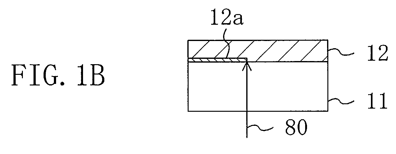
As shown in Figure 1B, after the epitaxial substrate is taken out of the reaction
chamber of the MOVPE apparatus, the mother substrate 11 is irradiated with laser light 80
from the surface opposite to the n-type contact layer 12, so that a thermally decomposed
layer 12a obtained by thermally decomposing the n-type contact layer 12 is formed at the
interface of the n-type contact layer 12 with the mother substrate 11. As the laser light 80,
for example, the third harmonics having a wavelength of 355 nm of so-called Nd:YAG laser
light, which can be obtained from crystals made of YAG (yttrium aluminum garnet) to
which neodymium ions (Nd3+) are added, is used. The irradiation energy at this time is
about 0.3 J/cm2, the interval between pulses is about 5 ns, and the spot diameter of the laser
light 80 during irradiation is about 100 µm.
-
Sapphire is transparent with respect to the laser light 80, and therefore the light
cannot be absorbed by the mother substrate 11. On the other hand, the wavelength of the
absorption edge in the forbidden band of gallium nitride is about 360 nm to 364 nm, so that
the wavelength of the laser light 80 is shorter and therefore the laser light 80 is absorbed in
the n-type contact layer 12. This absorption causes the n-type contact layer 12 to be
thermally decomposed into metal gallium (Ga) and nitrogen (N2) gas.
-
Therefore, as shown in Figure 1C, when the entire surface of the n-type contact
layer 12 is irradiated with the laser light 80, the mother substrate 11 and the n-type contact
layer 12 are attached while being in a melted state if the temperature is equal to or more than
the melting point (about 30°C) of the thermally decomposed layer 12a made of the metal
gallium. In order to maintain the attachment state without the mother substrate 11 and the
n-type contact layer 12 being not completely separated, the thermally decomposed layer 12a
should be generated in a suitable amount, and the suitable amount is determined by the
irradiation energy of the laser light 80. In this embodiment, the value of the irradiation
energy of the laser light 80 is set to about 0.1 J/cm2 or more and about 20 J/cm2 or less.
-
Next, as shown in Figure 1D, the epitaxial substrate with the n-type contact layer
12 attached is introduced again to the reaction chamber of the MOVPE apparatus, so that n-type
gallium nitride is further grown on the n-type contact layer 12 so as to increase the
thickness of the n-type contact layer 12 to about 20 µm. Then, an n-type barrier layer 13
made of n-type aluminum gallium nitride (Al0.3Ga0.7N) doped with silicon having a
thickness of about 0.1 µm, a light-emitting layer 14 made of undoped indium gallium nitride
(In0.2Ga0.8N) having a thickness of about 2nm, a p-type barrier layer 15 made of p-type
aluminum gallium nitride (Al0.3Ga0.7N) doped with magnesium (Mg) having a thickness of
about 0.1 µm, and a p-type contact layer 16 made of p-type gallium nitride doped with
magnesium having a thickness of about 0.5 µm are sequentially grown on the n-type contact
layer 12. Thus, a light-emitting diode element having a single quantum well structure in
which the light emitting layer 14 is sandwiched by the n-type barrier layer 13 and the p-type
barrier layer 15 is formed.
-
Next, as shown in Figure 1E, after the epitaxial substrate in which all the layers up
to the p-type contact layer 16 have been grown is taken out of the reaction chamber and
cooled to room temperature, a positive electrode 20 made of a laminated film of nickel (Ni)
and gold (Au) having a thickness of about 1 µm is formed selectively on the p-type contact
layer 16 by an evaporation method. Then, although not shown, a holding material made of
an adhesive tape material, a glass material, a resist material or other materials that are hardly
dissolved in hydrochloric acid (HCl) is attached, applied or plated onto the positive
electrode 20 and the p-type contact layer 16 in order to facilitate the handling of the epitaxial
layer after the mother substrate 11 is removed. Thereafter, the thermally decomposed layer
12a is removed with hydrochloric acid, so that the mother substrate 11 is separated from the
n-type contact layer 12. Then, a negative electrode 21 made of a laminated film of
titanium (Ti) and aluminum (Al) having a thickness of about 1 µm is formed by an
evaporation method on the surface of the n-type contact layer 12 to which the thermally
decomposed layer 12a was attached. Then, a light-emitting device can be obtained by
dividing the epitaxial layer into about 300 µm square chips, using a dicer. In this
embodiment, output light having a wavelength of 450 nm is obtained by applying a voltage
across the positive electrode 20 and the negative electrode 21. The holding material is
removed before or after the process for dividing the epitaxial layer in the form of a wafer
into chips.
-
Here, the order of the formation of the positive electrode 20 and the negative
electrode 21 does not matter. More specifically, when forming the negative electrode 21
before the positive electrode 20, first, the holding material is attached or applied onto the
upper surface of the p-type contact layer 16, and the mother substrate 11 is separated.
Thereafter, the negative electrode 21 is formed on the back surface of the n-type contact
layer 12. Thereafter, the holding material is removed and the positive electrode 20 is
formed on the p-type contact layer 16.
-
Thus, according to the first embodiment, a lower portion of the n-type contact layer
12 is formed on the mother substrate 11, and then the mother substrate 11 is irradiated with
the laser light 80 from the surface opposite to the n-type contact layer 12, so that the
thermally decomposed layer 12a obtained by thermally decomposing the n-type contact
layer 12 is formed at the interface of the n-type contact layer 12 with the mother substrate 11.
Therefore, the stress applied from the mother substrate 11 to the n-type contact layer 12
when the n-type contact layer 12 is grown again, the n-type barrier layer 13, the light-emitting
layer 14, the p-type barrier layer 15 and the p-type contact layer 16 are grown and
then the epitaxial substrate is cooled back to room temperature, which is caused by the
difference in the thermal expansion coefficient between the mother substrate 11 and the n-type
contact layer 12, can be reduced by the thermally decomposed layer 12a.
Consequently, the strain applied to the light-emitting layer 14 during cooling can be reduced,
so that the piezoelectric effect, which causes the recombination probability between
electrons and holes to be reduced, can be decreased, and therefore the light-emitting
efficiency can be improved. Furthermore, defects such as cracks occurring in the epitaxial
layer can be prevented.
-
Furthermore, the mother substrate 11 made of sapphire, which is hardly subjected
to processing, is removed and then dicing is performed, so that the wafer can be divided into
chips easily without cracks or fractures occurring, thus improving the yield.
-
Furthermore, since the mother substrate 11, which is an insulator, is removed, the
negative electrode 21 can be formed so as to oppose the positive electrode 20 on the surface
of the n-type contact layer 12 opposite to the light-emitting layer 14, so that the chip area
can be reduced.
-
Furthermore, since the mother substrate 11 having a small thermal conductivity is
removed, the heat release properties of the epitaxial layer are improved, so that the
temperature characteristics as a light-emitting diode device can be improved.
-
As the laser light 80, an excimer laser light having a wavelength of 248 nm with
krypton fluoride (KrF) can be used instead of the third harmonics of Nd:YAG laser light.
Second Embodiment
-
Hereinafter, a second embodiment of the present invention will be described with
reference to the accompanying drawings.
-
Figures 2A to 2E are cross-sectional views showing the process sequence in a
method for producing a light-emitting diode device, which is a semiconductor device of a
second embodiment of the present invention.
-
First, as shown in Figure 2A, for example, a mother substrate 11 made of sapphire
having the C plane as its principal plane and having a thickness of about 300 µm is
introduced into a MOVPE apparatus, and a buffer layer (not shown) made of gallium nitride
(GaN) having a thickness of about 20 nm, a p-type contact layer 22 made of gallium nitride
doped with magnesium, which is a p-type impurity, having a thickness of about 5 µm, and a
p-type barrier layer 23 made of p-type aluminum gallium nitride (Al0.3Ga0.7N) doped with
magnesium having a thickness of 0.1 µm are sequentially grown on the principal plane of
the introduced mother substrate 11.
-
As shown in Figure 2B, after the epitaxial substrate is taken out of a reaction
chamber of the MOVPE apparatus, the mother substrate 11 is irradiated with laser light 80
from the surface opposite to the p-type contact layer 22, so that a thermally decomposed
layer 22a obtained by thermally decomposing the p-type contact layer 22 is formed at the
interface of the p-type contact layer 22 with the mother substrate 11. As the laser light 80,
for example, the third harmonics of Nd:YAG laser light or KrF excimer laser light is used
The irradiation energy at this time is about 0.3 J/cm2, the interval between pulses is about 5
ns, and the spot diameter of the laser light 80 during irradiation is about 100 µm. The laser
light 80 is absorbed in the p-type contact layer 22, and this absorption causes the p-type
contact layer 22 to be thermally decomposed into metal gallium and nitrogen gas.
Therefore, when the entire surface of the p-type contact layer 22 is scanned by the laser light
80, as shown in Figure 2C, the mother substrate 11 and the p-type contact layer 22 are
attached by the thermally decomposed layer 22a.
-
In the second embodiment, after the p-type contact layer 22 and the p-type barrier
layer 23 are grown on the mother substrate 11, the p-type contact layer 22 is irradiated with
the laser light 80. Therefore, the p-type contact layer 22 and the p-type barrier layer 23 are
heated by the absorption of the laser light 80. Consequently, hydrogen (H), which causes
deactivation of the p-type acceptor made of magnesium, is desorbed from the p-type contact
layer 22 and the p-type barrier layer 23, so that the p-type acceptor becomes active. In
addition, there is an effect that the laser light 80 cleaves directly the bonding between
magnesium and hydrogen. Furthermore, the value of the irradiation energy of the laser
light 80 is set to about 0.1 J/cm2 or more and about 20 J/cm2 or less, so that the mother
substrate 11 is not completely separated from the p-type contact layer 22.
-
Next, as shown in Figure 2D, the epitaxial substrate with the p-type contact layer
22 and the p-type barrier layer 23 attached is introduced again to the reaction chamber of the
MOVPE apparatus. Then, a light-emitting layer 24 made of undoped indium gallium
nitride (In0.2Ga0.8N) having a thickness of about 2 nm, an n-type barrier layer 25 made of n-type
aluminum gallium nitride (Al0.3Ga0.7N) doped with silicon having a thickness of about
0.1 µm, and an n-type contact layer 26 made of n-type gallium nitride doped with silicon
having a thickness of about 0.5 µm are sequentially grown on the p-type barrier layer 23.
Thus, a light-emitting diode element having a single quantum well structure in which the
light emitting layer 24 is sandwiched by the p-type barrier layer 23 and the n-type barrier
layer 25 is formed.
-
Next, as shown in Figure 2E, after the epitaxial substrate in which all the layers up
to the n-type contact layer 26 have been grown is taken out of the reaction chamber and
cooled to room temperature, a negative electrode 21 made of a laminated film of titanium
and aluminum having a thickness of about 1 µm is formed selectively on the n-type contact
layer 26 by an evaporation method. Then, although not shown, a holding material made of
an adhesive tape material, a glass material, a resist material or other materials that are hardly
dissolved in hydrochloric acid (HCl) is attached, applied or plated onto the negative
electrode 21 and the n-type contact layer 26 in order to facilitate the handling of the epitaxial
layer after the mother substrate 11 is removed. Thereafter, the thermally decomposed layer
22a is removed with hydrochloric acid, so that the mother substrate 11 is separated from the
p-type contact layer 22. Then, a positive electrode 20 made of a laminated film of nickel
and gold having a thickness of about 1 µm is formed by an evaporation method on the
surface of the p-type contact layer 22 to which the thermally decomposed layer 22a was
attached. The order of the formation of the positive electrode 20 and the negative electrode
21 does not matter in this case as well. Thereafter, a light-emitting device can be obtained
by dividing the epitaxial layer into about 300 µm square chips, using a dicer. In this
embodiment, output light having a wavelength of 450 nm is obtained by applying a voltage
across the positive electrode 20 and the negative electrode 21. The holding material is
removed before or after the process for dividing the epitaxial layer into chips.
-
Thus, according to the second embodiment, the p-type contact layer 22 and the p-type
barrier layer are formed on the mother substrate 11, and then the mother substrate 11 is
irradiated with the laser light 80 from the surface opposite to the p-type contact layer 22, so
that the thermally decomposed layer 22a obtained by thermally decomposing the p-type
contact layer 22 is formed at the interface of the p-type contact layer 22 with the mother
substrate 11. Therefore, the stress applied from the mother substrate 11 to the p-type
contact layer 22 when the light-emitting layer 24, the n-type barrier layer 25 and the n-type
contact layer 26 are grown on the p-type barrier layer 23 and then the epitaxial substrate is
cooled back to room temperature, which is caused by the difference in the thermal
expansion coefficient between the mother substrate 11 and the p-type contact layer 22, can
be reduced by the thermally decomposed layer 22a. Consequently, the strain applied to the
light-emitting layer 24 during cooling can be reduced, so that the piezoelectric effect, which
causes the recombination probability between electrons and holes to be reduced, can be
decreased, and therefore the light-emitting efficiency can be improved. Furthermore,
defects such as cracks occurring in the epitaxial layer can be prevented.
-
In addition, unlike the first embodiment, since the thermal deposition layer 22a is
formed in the p-type contact layer 22 by the laser light 80, the heat generated in the p-type
contact layer 22 during irradiation of the laser light 80 activates the p-type acceptor in the p-type
contact layer 22 and the p-type barrier layer 23 thereon. Therefore, the process for
activating the acceptor by a heat treatment for activation or electron beam irradiation or the
like can be eliminated.
Third Embodiment
-
Hereinafter, a third embodiment of the present invention will be described with
reference to the accompanying drawings.
-
Figures 3A to 3E are cross-sectional views showing the process sequence in a
method for producing a semiconductor laser device, which is a semiconductor device of a
third embodiment of the present invention.
-
First, as shown in Figure 3A, a mother substrate 11 made of sapphire having the C
plane as its principal plane and having a thickness of about 300 µm is introduced into, for
example, an MOVPE apparatus, and a buffer layer (not shown) made of gallium nitride
(GaN) having a thickness of about 20 nm and an n-type contact layer 32 made of n-type
gallium nitride doped with silicon having a thickness of about 5 µm are sequentially grown
on the principal plane of the introduced mother substrate 11.
-
As shown in Figure 3B, after the epitaxial substrate is taken out of the reaction
chamber of the MOVPE apparatus, the mother substrate 11 is irradiated with laser light 80
from the surface opposite to the n-type contact layer 32, so that a thermally decomposed
layer 32a obtained by thermally decomposing the n-type contact layer 32 is formed at the
interface of the n-type contact layer 32 with the mother substrate 11. As the laser light 80,
for example, the third harmonics of Nd:YAG laser light or KrF excimer laser light is used
The irradiation energy at this time is about 0.3 J/cm2, the interval between pulses is about 5
ns, and the spot diameter of the laser light 80 during irradiation is about 100 µm. The laser
light 80 is absorbed in the n-type contact layer 32, and this absorption causes the n-type
contact layer 32 to be thermally decomposed into metal gallium and nitrogen gas.
Therefore, as shown in Figure 3C, when the entire surface of the n-type contact layer 32 is
scanned by the laser light 80, the mother substrate 11 and the n-type contact layer 32 are
attached by the thermally decomposed layer 32a. In this embodiment, the value of the
irradiation energy of the laser light 80 is set to about 0.1 J/cm2 or more and about 20 J/cm2
or less, so that the mother substrate 11 is not completely separated from the n-type contact
layer 32.
-
Next, as shown in Figure 3D, the epitaxial substrate with the n-type contact layer
32 attached is introduced again to the reaction chamber of the MOVPE apparatus, so that n-type
gallium nitride is further grown on the n-type contact layer 32 so as to increase the
thickness of the n-type contact layer 32 to about 20 µm. Then, a first cladding layer 33
made of n-type aluminum gallium nitride (Al0.15Ga0.85N) doped with silicon having a
thickness of about 1 µm, a first optical guide layer 34 made of undoped gallium nitride
having a thickness of about 0.1 µm, a quantum well active layer 35, a second optical guide
layer 36 made of undoped gallium nitride having a thickness of about 0.1 µm, a second
cladding layer 37 made of p-type aluminum gallium nitride (Al0.15Ga0.85N) doped with
magnesium having a thickness of about 1 µm, and a p-type contact layer 38 made of p-type
gallium nitride doped with magnesium having a thickness of about 0.3 µm are sequentially
grown on the n-type contact layer 32.
-
In this embodiment, although not shown, the quantum well active layer 35 has a
multiple quantum well structure in which a well layer made of indium gallium nitride
(In0.15Ga0.85N) having a thickness of about 3 nm, and a barrier layer made of indium gallium
nitride (In0.02Ga0.98N) having a thickness of about 7 nm are formed repeatedly for 3 cycles.
Thus, a semiconductor laser element having a multiple quantum well structure in which the
quantum well active layer 35 is sandwiched by the n-type first cladding layer 33 and the p-type
second cladding layer 37 is formed.
-
Next, as shown in Figure 3E, after the epitaxial substrate in which all the layers up
to the p-type contact layer 38 have been grown is taken out of the reaction chamber and
cooled to room temperature, a positive electrode 20 made of a laminated film of nickel and
gold having a thickness of about 1 µm is formed on the p-type contact layer 38 by an
evaporation method. Furthermore, the positive electrode 20 is patterned in a stripe by dry
etching or the like, so as to serve as a wave guide of the quantum well active layer 35.
Then, although not shown, a holding material made of an adhesive tape material, a glass
material, a resist material or other materials that are hardly dissolved in hydrochloric acid is
attached (applied) onto the positive electrode 20 and the p-type contact layer 38 in order to
facilitate the handling of the epitaxial layer after the mother substrate 11 is removed.
Thereafter, the thermally decomposed layer 32a is removed with hydrochloric acid, so that
the mother substrate 11 is separated from the n-type contact layer 32. Then, a negative
electrode 21 made of a laminated film of titanium and aluminum having a thickness of about
1 µm is formed by an evaporation method on the surface of the n-type contact layer 32 to
which the thermally decomposed layer 32a was attached. Furthermore, the negative
electrode 21 is patterned so as to oppose the positive electrode 20. Herein as well, the
order of the formation of the positive electrode 20 and the negative electrode 21 does not
matter.
-
Then, for example, the n-type contact layer 32 of the epitaxial layer is scribed by a
point scriber so that the (-1100) plane and the (1-100) plane of the orientations in the
epitaxial layer (quantum well active layer 35) serve as the end faces of a resonator, and a
weight is added along the scribe line and the epitaxial layer is cleaved. Thus, a desired
laser chip can be obtained from the epitaxial layer. The light generated in the quantum
well active layer 35 of the laser chip is reflected and resonated by the end face of the
resonator and is released as laser light. Herein, the distance between the end faces of a
resonator is about 500 µm, and the holding material for holding the epitaxial layer is
removed before or after the process for dividing the epitaxial layer into chips.
-
In this specification, the minus sign "-" attached to Miller indices included in the
orientation represents the reversal of the index following the minus sign for convenience.
-
The thus obtained laser chip was held on a heat sink with the positive electrode 20
at the upper surface (p-side up), and the electrodes 20 and 21 were wire-bonded and laser
oscillation was performed. Then, it was confirmed that the laser light having an oscillation
wavelength of 405 nm can be oscillated continuously at room temperature.
-
Thus, according to the third embodiment, a lower portion of the n-type contact
layer 32 is formed on the mother substrate 11, and then the mother substrate 11 is irradiated
with the laser light 80 from the surface opposite to the n-type contact layer 32. Thus, the
thermally decomposed layer 32a obtained by thermally decomposing the n-type contact
layer 32 is formed at the interface of the n-type contact layer 32 with the mother substrate 11.
Therefore, the stress applied from the mother substrate 11 to the n-type contact layer 32
when the n-type contact layer 32 is grown again, the semiconductor layers including the
quantum well active layer 35 are further grown thereon and then the epitaxial substrate is
cooled back to room temperature, which is caused by the difference in the thermal
expansion coefficient between the mother substrate 11 and the n-type contact layer 32, can
be reduced reliably by the thermally decomposed layer 32a. Consequently, the strain
applied to the quantum well active layer 35 during cooling can be reduced, so that the
piezoelectric effect, which causes the recombination probability between electrons and holes
to be reduced, can be decreased, and therefore the light-emitting efficiency can be improved.
Furthermore, defects such as cracks occurring in the epitaxial layer can be prevented.
-
Furthermore, the mother substrate 11 made of sapphire, which is hardly subjected
to processing, is removed and then cleavage is performed, so that the wafer can be divided
into chips easily without cracks or fractures occurring, thus improving the yield.
-
Furthermore, since the mother substrate 11, which is an insulator, is removed, the
negative electrode 21 can be formed so as to oppose the positive electrode 20 on the surface
of the n-type contact layer 32 opposite to the quantum well active layer 35, so that the chip
area can be reduced. As a result, a large number of laser elements can be obtained from
one wafer.
-
Furthermore, since the mother substrate 11 having a small thermal conductivity and
a thickness of several hundreds of µm is removed, the volume per element can be reduced,
which facilitates achieving compactness. In addition, the heat release properties of the
epitaxial layer are improved, so that the temperature characteristics as a semiconductor laser
device can be improved, so that the life of the elements can be improved remarkably.
Fourth Embodiment
-
Hereinafter, a fourth embodiment of the present invention will be described with
reference to the accompanying drawings.
-
Figures 4A to 4F are cross-sectional views showing the process sequence in a
method for producing a semiconductor laser device, which is a semiconductor device of a
fourth embodiment of the present invention.
-
First, as shown in Figure 4A, a mother substrate 11 made of sapphire having the C
plane as its principal plane and having a thickness of about 300 µm is introduced into, for
example, an MOVPE apparatus, and a buffer layer (not shown) made of gallium nitride
(GaN) having a thickness of about 20 nm and an n-type underlying layer 31 made of n-type
gallium nitride doped with silicon having a thickness of about 5 µm are sequentially grown
on the principal plane of the introduced mother substrate 11. Then, the epitaxial substrate
is taken out of the reaction chamber, and thereafter a dielectric film made of silicon oxide
(SiO2) having a thickness of about 100 nm is deposited on the entire surface of the n-type
underlying layer 31 by sputtering or CVD. Subsequently, a mask film 81 having a 5 µm
stripe shape for both the width and the gap in which the stripe is extending in the <11-20>
direction of the zone axis of the gallium nitride constituting the n-type underlying layer 31 is
formed from the deposited dielectric film by lithography and wet etching using hydrofluoric
acid (HF) as an etchant.
-
Then, as shown in Figure 4B, the mother substrate 11 is irradiated with laser light
80 from the surface opposite to the n-type underlying layer 31, so that a thermally
decomposed layer 31a obtained by thermally decomposing the n-type underlying layer 31 is
formed at the interface of the n-type underlying layer 31 with the mother substrate 11. As
the laser light 80, for example, the third harmonics of Nd:YAG laser light or KrF excimer
laser light is used The irradiation energy at this time is about 0.3 J/cm2, the interval
between pulses is about 5 ns, and the spot diameter of the laser light 80 during irradiation is
about 100 µm. The laser light 80 is absorbed in the n-type underlying layer 31, and this
absorption causes the n-type underlying layer 31 to be thermally decomposed into metal
gallium and nitrogen gas. Therefore, as shown in Figure 4C, when the entire surface of the
n-type underlying layer 31 is scanned by the laser light 80, the mother substrate 11 and the
n-type underlying layer 31 are attached by the thermally decomposed layer 31a. In this
embodiment, the value of the irradiation energy of the laser light 80 is set to about 0.1 J/cm2
or more and about 20 J/cm2 or less, so that the mother substrate 11 is not completely
separated from the n-type underlying layer 31.
-
Next, as shown in Figure 4D, the epitaxial substrate with the n-type underlying
layer 31 attached is introduced again to the reaction chamber of the MOVPE apparatus, so
that n-type gallium nitride doped with silicon is grown on the n-type underlying layer 31
using the mask film 81 as a mask for selective growth to form an n-type contact layer 32
having a thickness of about 15 µm. In this case, the gallium nitride constituting the n-type
contact layer 32 has a different crystal structure than that of the silicon oxide constituting the
mask film 81, so that crystal grown is not caused on the mask film 81 and crystal grown
starts in the exposed portions from the openings of the mask film 81 in the n-type
underlying layer 31. When the crystals are further grown, the n-type contact layer 32
grown from the openings of the mask film 81 start to be grown in the traverse direction
(direction parallel to the substrate surface) in the portion above the mask film 81, until the
portion of the n-type contact layer 32 grown from the openings of the mask film 81 covers
the mask film 81. Herein, a dislocation generated by a lattice mismatch with respect to the
mother substrate 11 is present in a direction substantially perpendicular to the substrate
surface in the portion of the n-type contact layer 32 grown above the openings of the mask
film 81. On the other hand, in the portion of the n-type contact layer 32 above the mask
film 81, the dislocation (defect) present in the n-type contact layer 32 is prevented from
propagating by the mask film 81, so that the dislocation density is small. For example, the
dislocation density of the n-type contact layer 32 of the fourth embodiment is one or two
orders smaller than that of the n-type contact layer 32 of the third embodiment.
-
Furthermore, as shown in Figure 4E, a first cladding layer 33 made of n-type
aluminum gallium nitride (Al0.15Ga0.85N) doped with silicon having a thickness of about 1
µm, a first optical guide layer 34 made of undoped gallium nitride having a thickness of
about 0.1 µm, a quantum well active layer 35, a second optical guide layer 36 made of
undoped gallium nitride having a thickness of about 0.1 µm, a second cladding layer 37
made of p-type aluminum gallium nitride (Al0.1Ga0.9N) doped with magnesium having a
thickness of about 1 µm, and a p-type contact layer 38 made of p-type gallium nitride doped
with magnesium having a thickness of about 0.3 µm are sequentially grown on the n-type
contact layer 32. In this case, the quantum well active layer 35 has the same multiple
quantum well structure as in the third embodiment.
-
Next, as shown in Figure 4F, after the epitaxial substrate in which all the layers up
to the p-type contact layer 38 have been grown is taken out of the reaction chamber and
cooled to room temperature, a positive electrode 20 made of a laminated film of nickel and
gold having a thickness of about 1 µm is formed on the p-type contact layer 38 by an
evaporation method. Furthermore, the positive electrode 20 is patterned in a stripe by dry
etching or the like, so as to serve as a wave guide of the quantum well active layer 35.
Then, although not shown, a holding material made of an adhesive tape material, a glass
material, a resist material or other materials that are hardly dissolved in hydrochloric acid is
attached, applied or plated onto the positive electrode 20 and the p-type contact layer 38 in
order to facilitate the handling of the epitaxial layer after the mother substrate 11 is removed.
Thereafter, the thermally decomposed layer 31a is removed with hydrochloric acid, so that
the mother substrate 11 is separated from the n-type underlying layer 31. Subsequently, the
n-type underlying layer 31 and the mask film 81 are removed by polishing such as chemical
mechanical polishing (CMP). Then, a negative electrode 21 made of a laminated film of
titanium and aluminum having a thickness of about 1 µm is formed by an evaporation
method on the surface of the n-type contact layer 32 opposite to the positive electrode 20.
Furthermore, the negative electrode 21 is patterned so as to oppose the positive electrode 20.
Herein as well, the order of the formation of the positive electrode 20 and the negative
electrode 21 does not matter.
-
Then, for example, the n-type contact layer 32 of the epitaxial layer is scribed by a
point scriber so that the (-1100) plane and the (1-100) plane of the orientations in the
epitaxial layer serve (quantum well active layer 35) as the end faces of a resonator, and a
weight is added along the scribe line and the epitaxial layer is cleaved. Thus, a desired
laser chip can be obtained from the epitaxial layer. Herein, the distance between the end
faces of a resonator is about 500 µm, and the holding material for holding the epitaxial layer
is removed before or after the process for dividing the epitaxial layer into chips.
-
The thus obtained laser chip was held on a heat sink with the p-side up, and the
electrodes 20 and 21 were wire-bonded and laser oscillation was performed. Then, it was
confirmed that the laser light having an oscillation wavelength of 405 nm can be oscillated
continuously at room temperature.
-
Thus, according to the fourth embodiment, the n-type underlying layer 31 that is a
layer underlying the n-type contact layer 32 is formed on the mother substrate 11, and then
the mother substrate 11 is irradiated with the laser light 80 from the surface opposite to the
n-type underlying layer 31, so that the thermally decomposed layer 31a obtained by
thermally decomposing the n-type underlying layer 31 is formed at the interface of the n-type
underlying layer 31 with the mother substrate 11. Therefore, the stress applied from
the mother substrate 11 to the n-type underlying layer 31 when the n-type contact layer 32 is
grown on the n-type underlying layer 31 and further the semiconductor layers including the
quantum well active layer 35 are grown and then the epitaxial substrate is cooled back to
room temperature, which is caused by the difference in the thermal expansion coefficient
between the mother substrate 11 and the n-type underlying layer 31, can be reduced by the
thermally decomposed layer 31a.
-
In addition, the n-type contact layer 32 of the fourth embodiment is selectively
grown from the n-type underlying layer 31 exposed from the openings of the mask film 81
made of a material that substantially prevents gallium nitride from being grown (selective
growth in the traverse direction). Therefore, the dislocation density is significantly reduced.
As a result, the crystallinity of the epitaxial layer including the quantum well active layer 35
is improved, so that the operational characteristics of the semiconductor laser device is
significantly improved.
-
The shape of the mask film 81 is a stripe, but is not limited thereto, and the same
effect can be obtained with dotted shapes or lattice shapes.
Fifth Embodiment
-
Hereinafter, a fifth embodiment of the present invention will be described with
reference to the accompanying drawings.
-
Figures 5A to 5F are cross-sectional views showing the process sequence in a
method for producing a semiconductor laser device, which is a semiconductor device of a
fifth embodiment of the present invention.
-
First, as shown in Figure 5A, a dielectric film made of silicon oxide having a
thickness of about 100 nm is deposited on a mother substrate 11 made of sapphire having
the C plane as its principal plane and having a thickness of about 300 µm by, for example,
sputtering or CVD. Subsequently, a mask film 81 having a 5 µm stripe shape for both the
width and the gap in which the stripe is extending in the <1-100> direction of the zone axis
of the sapphire constituting the mother substrate 11 is formed from the deposited dielectric
film by lithography and wet etching using hydrofluoric acid as an etchant.
-
Then, as shown in Figure 5B, the mother substrate 11 provided with the mask film
81 is introduced into the reaction chamber of the MOVPE apparatus, and n-type gallium
nitride is grown using the mask film 81 as a mask for selective growth, so that a buffer layer
(not shown) having a thickness of about 30 nm is formed. Then, n-type gallium nitride
doped with silicon is grown on the buffer layer so that the n-type underlying layer 31 having
a thickness of about 5 µm is formed. Herein, the n-type underlying layer 31 is configured
so as to include the buffer layer. In this case, the gallium nitride constituting the n-type
underlying layer 31 is not crystal-grown on the mask film 81 and starts to be grown in the
exposed portions from the openings of the mask film 81 in the n-type underlying layer 31.
When the crystals are further grown, the n-type underlying layer 31 grown from the
openings of the mask film 81 start to be grown in the traverse direction (direction parallel to
the substrate surface) in the portion above the mask film 81, until the portion of the n-type
underlying layer 31 grown from the openings of the mask film 81 covers the mask film 81.
Herein, a dislocation generated by a lattice mismatch with respect to the mother substrate 11
is present in a direction substantially perpendicular to the substrate surface in the portion of
the n-type underlying layer 31 grown above the openings of the mask film 81. On the
other hand, in the portion of the n-type underlying layer 31 above the mask film 81, the
dislocation (defect) present in the n-type underlying layer 31 is prevented from propagating
by the mask film 81, so that the dislocation is low.
-
Then, as shown in Figure 5C, after the epitaxial substrate is taken out of the
reaction chamber of the MOVPE apparatus, the mother substrate 11 is irradiated with laser
light 80 from the surface opposite to the n-type underlying layer 31, so that a thermally
decomposed layer 31a obtained by thermally decomposing the n-type underlying layer 31 is
formed at the interface of the n-type underlying layer 31 with the mother substrate 11 and in
the vicinity of the mask film 81. As the laser light 80, for example, the third harmonics of
Nd:YAG laser light or KrF excimer laser light is used The irradiation energy at this time is
about 0.3 J/cm2, the interval between pulses is about 5 ns, and the spot diameter of the laser
light 80 during irradiation is about 100 µm. The laser light 80 is not absorbed in the silicon
oxide film (mask film 81) but is absorbed in the n-type underlying layer 31 since silicon
oxide has a wavelength of 190 nm at the absorption edge. This absorption causes the n-type
underlying layer 31 to be thermally decomposed into metal gallium and nitrogen gas.
Therefore, as shown in Figure 5D, when the entire surface of the n-type underlying layer 31
is scanned by the laser light 80, the mother substrate 11 and the n-type underlying layer 31
are attached by the thermally decomposed layer 31a. In this case, the value of the
irradiation energy of the laser light 80 is set to about 0.1 J/cm2 or more and about 20 J/cm2
or less, so that the mother substrate 11 is not completely separated from the n-type
underlying layer 31.
-
Next, as shown in Figure 5E, the epitaxial substrate with the n-type underlying
layer 31 attached is introduced again to the reaction chamber of the MOVPE apparatus.
Subsequently, an n-type contact layer 32 made of n-type gallium nitride doped with silicon
having a thickness of about 15 µm, a first cladding layer 33 made of n-type aluminum
gallium nitride (Al0.15Ga0.85N) doped with silicon having a thickness of about 1 µm, a first
optical guide layer 34 made of undoped gallium nitride having a thickness of about 0.1 µm,
a quantum well active layer 35, a second optical guide layer 36 made of undoped gallium
nitride having a thickness of about 0.1 µm, a second cladding layer 37 made of p-type
aluminum gallium nitride (Al0.1Ga0.9N) doped with magnesium having a thickness of about
1 µm, and a p-type contact layer 38 made of p-type gallium nitride doped with magnesium
having a thickness of about 0.3 µm are sequentially grown on the n-type underlying layer 31.
In this case, the quantum well active layer 35 has the same multiple quantum well structure
as in the third embodiment.
-
Next, as shown in Figure 5F, after the epitaxial substrate in which all the layers up
to the p-type contact layer 38 have been grown is taken out of the reaction chamber and
cooled to room temperature, a positive electrode 20 made of a laminated film of nickel and
gold having a thickness of about 1 µm is formed on the p-type contact layer 38 by an
evaporation method. Furthermore, the positive electrode 20 is patterned in a stripe by dry
etching or the like, so as to serve as a wave guide of the quantum well active layer 35.
Then, although not shown, a holding material made of an adhesive tape material, a glass
material, a resist material or other materials that are hardly dissolved in hydrochloric acid is
attached, applied or plated onto the positive electrode 20 and the p-type contact layer 38 in
order to facilitate the handling of the epitaxial layer after the mother substrate 11 is removed.
Thereafter, the thermally decomposed layer 31a is removed with hydrochloric acid, so that
the mother substrate 11 is separated from the n-type underlying layer 31, and then, the n-type
underlying layer 31 and the mask film 81 are polished and removed by a CMP method.
Then, a negative electrode 21 made of a laminated film of titanium and aluminum having a
thickness of about 1 µm is formed by an evaporation method on the surface of the n-type
underlying layer 31 to which the thermal decomposition film 31a was attached.
Furthermore, the negative electrode 21 is patterned so as to oppose the positive electrode 20.
Herein as well, the order of the formation of the positive electrode 20 and the negative
electrode 21 does not matter. Then, for example, the n-type contact layer 32 of the
epitaxial layer is scribed by a point scriber so that the (-1100) plane and the (1-100) plane of
the orientations in the epitaxial layer (quantum well active layer 35) serve as the end faces of
a resonator, and a weight is added along the scribe line and the epitaxial layer is cleaved.
Thus, a desired laser chip can be obtained from the epitaxial layer. Herein, the distance
between the end faces of a resonator is about 500 µm, and the holding material for holding
the epitaxial layer is removed before or after the process for dividing the epitaxial layer into
chips.
-
The thus obtained laser chip was held on a heat sink with the p-side up, and the
electrodes 20 and 21 were wire-bonded and laser oscillation was performed. Then, it was
confirmed that the laser light having an oscillation wavelength of 405 nm can be oscillated
continuously at room temperature.
-
Thus, according to the fifth embodiment, after the mask film 81 for selective
growth is formed on the mother substrate 11, the n-type underlying layer 31 that is a layer
underlying the n-type contact layer 32 is selectively grown. Thereafter, the mother
substrate 11 is irradiated with the laser light 80 from the surface opposite to the n-type
underlying layer 31, so that the thermally decomposed layer 31a obtained by thermally
decomposing the n-type underlying layer 31 is formed at the interface of the n-type
underlying layer 31 with the mother substrate 11. Therefore, the stress applied from the
mother substrate 11 to the n-type underlying layer 31 when the n-type contact layer 32 is
grown on the n-type underlying layer 31 and further the semiconductor layers including the
quantum well active layer 35 are grown and then the epitaxial substrate is cooled back to
room temperature, which is caused by the difference in the thermal expansion coefficient
between the mother substrate 11 and the n-type underlying layer 31, can be reduced by the
thermally decomposed layer 31a.
-
In addition, the n-type underlying layer 31 of the fifth embodiment is selectively
grown from the mother substrate 11 exposed from the openings of the mask film 81 made of
a material that substantially prevents gallium nitride from being grown (selective growth in
the traverse direction). Therefore, the dislocation density is significantly reduced. As a
result, the crystallinity of the epitaxial layer including the quantum well active layer 35 is
improved, so that the operational characteristics of the semiconductor laser device is
significantly improved.
-
The shape of the mask film 81 is a stripe, but is not limited thereto, and the same
effect can be obtained with dotted shapes or lattice shapes.
Sixth Embodiment
-
Hereinafter, a sixth embodiment of the present invention will be described with
reference to the accompanying drawings.
-
Figures 6A to 6E are cross-sectional views showing the process sequence in a
method for producing a semiconductor laser device, which is a semiconductor device of a
sixth embodiment of the present invention.
-
First, as shown in Figure 6A, a mother substrate 11 made of sapphire having the C
plane as its principal plane and having a thickness of about 300 µm is introduced into an
MOVPE apparatus, so that a buffer layer (not shown) made of aluminum gallium nitride
(Al0.15Ga0.85N) having a thickness of about 20 nm and an n-type contact layer 42 made of
aluminum gallium nitride (Al0.15Ga0.85N) doped with silicon having a thickness of about 1
µm are sequentially grown on the principal plane of the introduced mother substrate 11.
The n-type contact layer 42 is configured to as to include the buffer layer.
-
As shown in Figure 6B, after the epitaxial substrate is taken out of the reaction
chamber of the MOVPE apparatus, the mother substrate 11 is irradiated with laser light 80
from the surface opposite to the n-type contact layer 42, so that a thermally decomposed
layer 42a obtained by thermally decomposing the n-type contact layer 42 is formed at the
interface of the n-type contact layer 42 with the mother substrate 11. As the laser light 80,
for example, KrF excimer laser light of a wavelength of 248 nm is used. The irradiation
energy at this time is about 0.3 J/cm2, the interval between pulses is about 5 ns, and the spot
diameter of the laser light 80 during irradiation is about 100 µm. Sapphire is transparent
with respect to the laser light 80, and therefore the light cannot be absorbed by the mother
substrate 11. On the other hand, the wavelength of the absorption edge in the forbidden
band of the aluminum gallium nitride (Al0.15Ga0.85N) is about 330 nm to 340 nm, so that the
wavelength of the laser light 80 is shorter and therefore the laser light 80 is absorbed in the
n-type contact layer 42. This absorption causes the n-type contact layer 42 to be thermally
decomposed into gallium, aluminum and nitrogen gas. Wherein, the thermally
decomposed layer 42a is made of an alloy of gallium and aluminum of which melting point
is lower than that of pure gallium. Therefore, in this case, the value of the irradiation
energy of the laser light 80 is set to about 0.1 J/cm2 or more and about 20 J/cm2 or less, so
that as described above, the mother substrate 11 and the n-type contact layer 42 are attached
by the thermally decomposed layer 42a in a melted state if the temperature is equal to or
more than the melting point of the alloy. Therefore, as shown in Figure 6C, when the
entire surface of the n-type contact layer 42 is scanned by the laser light 80, the mother
substrate 11 and the n-type contact layer 42 are attached by the thermally decomposed layer
42a.
-
Next, as shown in Figure 6D, the epitaxial substrate with the n-type contact layer
42 attached is introduced again to the reaction chamber of the MOVPE apparatus.
Subsequently, a first cladding layer 43 made of n-type aluminum gallium nitride
(Al0.15Ga0.85N) doped with silicon having a thickness of about 20 µm, a first optical guide
layer 44 made of undoped gallium nitride having a thickness of about 0.1 µm, a quantum
well active layer 45, a second optical guide layer 46 made of undoped gallium nitride having
a thickness of about 0.1 µm, a second cladding layer 47 made of p-type aluminum gallium
nitride (Al0.15Ga0.85N) doped with magnesium having a thickness of about 1.5 µm, and a p-type
contact layer 48 made of p-type gallium nitride doped with magnesium having a
thickness of about 0.3 µm are sequentially grown on the n-type contact layer 42. In this
embodiment as well as in the third embodiment, the quantum well active layer 45 has a
structure in which a well layer made of indium gallium nitride (In0.15Ga0.85N) having a
thickness of about 3 nm, and a barrier layer made of indium gallium nitride (In0.02Ga0.98N)
having a thickness of about 7 nm are formed repeatedly for 3 cycles.
-
Next, as shown in Figure 6E, after the epitaxial substrate in which all the layers up
to the p-type contact layer 48 have been grown is taken out of the reaction chamber and
cooled to room temperature, a positive electrode 20 made of a laminated film of nickel and
gold having a thickness of about 1 µm is formed on the p-type contact layer 48 by an
evaporation method. Furthermore, the positive electrode 20 is patterned in a stripe by dry
etching or the like, so as to serve as a wave guide of the quantum well active layer 45.
Then, although not shown, a holding material made of an adhesive tape material, a glass
material, a resist material or other materials that are hardly dissolved in hydrochloric acid is
attached, applied or plated onto the positive electrode 20 and the p-type contact layer 48 in
order to facilitate the handling of the epitaxial layer after the mother substrate 11 is removed.
Thereafter, the thermally decomposed layer 42a is removed with hydrochloric acid, so that
the mother substrate 11 is separated from the n-type contact layer 42. Then, a negative
electrode 21 made of a laminated film of titanium and aluminum having a thickness of about
1 µm is formed by an evaporation method on the surface of the n-type contact layer 42 to
which the thermally decomposed layer 42a was attached. Furthermore, the negative
electrode 21 is patterned so as to oppose the positive electrode 20. Herein as well, the
order of the formation of the positive electrode 20 and the negative electrode 21 does not
matter.
-
Then, for example, the n-type contact layer 32 of the epitaxial layer is scribed by a
point scriber so that the (-1100) plane and the (1-100) plane of the orientations in the
epitaxial layer serve (quantum well active layer 45) as the end faces of a resonator, and a
weight is added along the scribe line and the epitaxial layer is cleaved. Thus, a desired
laser chip can be obtained from the epitaxial layer. The light generated in the quantum
well active layer 45 of the laser chip is reflected and resonated by the end face of the
resonator and is released as laser light. Herein, the distance between the end faces of a
resonator is about 500 µm, and the holding material for holding the epitaxial layer is
removed before or after the process for dividing the epitaxial layer into chips.
-
As described above, in the sixth embodiment, the first semiconductor layer (n-type
contact layer 42) is grown on the mother substrate 11, and then the first semiconductor layer
is irradiated with the laser light 80 that can thermally decompose the first semiconductor
layer from the side of mother substrate 11. Thus, the thermally decomposed layer 42a for
attaching the interfaces of the mother substrate 11 and the first semiconductor layer while
breaking the joining of the mother substrate 11 and the first semiconductor layer is formed.
Thus, in the cooling process after the growth of the epitaxial layer shown in Figure 6D, the
stress caused by the difference in the thermal expansion coefficient between the mother
substrate 11 and the first semiconductor layer can be reduced.
-
In general, when an aluminum gallium nitride (AlGaN) layer is grown on a gallium
nitride (GaN) layer, cracks are likely to occur because of the lattice mismatch between the
gallium nitride crystals and the aluminum gallium nitride crystals, so that the thickness
cannot be increased. In addition, when the composition of the aluminum is increased to
increase the forbidden band (band gap) of the semiconductor layer made of aluminum
gallium nitride, the mismatch is further increased, and therefore the critical film thickness as
crystal is reduced.
-
However, according to the sixth embodiment, the n-type contact layer 42 made of
aluminum gallium nitride is grown to a thickness of not more than the critical film thickness,
and then the n-type contact layer 42 is irradiated with the laser light 80, so that the stress
applied from the mother substrate 11 can be reduced. Therefore, there is no possibility that
cracks occurs in the n-type contact layer 42. Furthermore, after the irradiation of the laser
light 80, the thermally decomposed layer 42a produced by thermal decomposition allows
the n-type contact layer 42 to be in the state in which a stress applied from the mother
substrate 11 is reduced, so that even if the first cladding layer 43 made of n-type aluminum
gallium is grown to a comparatively large thickness on the n-type contact layer 42, there is
no possibility that cracks occur in the first cladding layer 43.
-
Furthermore, even if the composition of the aluminum of the n-type contact layer
42 is further increased, no cracks occur in the n-type contact layer 42 and the first cladding
layer 43, as long as the n-type contact layer 42 is irradiated with the laser light 80 after being
grown to a thickness of not more than the critical film thickness. Therefore, it is possible
to form the first cladding layer 43 having a large composition of aluminum and a large
thickness, so that the ability of confining generated light and carriers of the quantum well
active layer 45 can be improved.
-
In order to confine sufficiently generated light in the quantum well active layer 45,
it is preferable that the composition of aluminum of the first cladding layer 43 is 0.05 or
more, and that the thickness thereof including the n-type contact layer 42 is 0.5 µm or more.
-
In addition, gallium nitride may be used for the buffer layer in lieu to aluminum
gallium nitride.
Seventh Embodiment
-
Hereinafter, a seventh embodiment of the present invention will be described with
reference to the accompanying drawings.
-
Figures 7A to 7E are cross-sectional views showing the process sequence in a
method for producing a surface-light-emitting laser device, which is a semiconductor device
of a seventh embodiment of the present invention.
-
First, as shown in Figure 7A, a mother substrate 11 made of sapphire having the C
plane as its principal plane and having a thickness of about 300 µm is introduced into, for
example an MOVPE apparatus, and a buffer layer (not shown) made of gallium nitride
having a thickness of about 20 nm and an n-type contact layer 52 made of n-type gallium
nitride doped with silicon having a thickness of about 5 µm are sequentially grown on the
principal plane of the introduced mother substrate 11.
-
As shown in Figure 7B, after the epitaxial substrate is taken out of the reaction
chamber of the MOVPE apparatus, the mother substrate 11 is irradiated with laser light 80
from the surface opposite to the n-type contact layer 52, so that a thermally decomposed
layer 52a obtained by thermally decomposing the n-type contact layer 52 is formed at the
interface of the n-type contact layer 52 with the mother substrate 11. As the laser light 80,
for example, the third harmonics of Nd:YAG laser light or KrF excimer laser light is used.
The irradiation energy at this time is about 0.3 J/cm2, the interval between pulses is about 5
ns, and the spot diameter of the laser light 80 during irradiation is about 100 µm. The laser
light 80 is absorbed in the n-type contact layer 52, and this absorption causes the n-type
contact layer 52 to be thermally decomposed into metal gallium and nitrogen gas.
Therefore, as shown in Figure 7C, when the entire surface of the n-type contact layer 52 is
scanned by the laser light 80, the mother substrate 11 and the n-type contact layer 52 are
attached by the thermally decomposed layer 52a. In this embodiment, the value of the
irradiation energy of the laser light 80 is set to about 0.1 J/cm2 or more and about 20 J/cm2
or less, so that the mother substrate 11 is not completely separated from the n-type contact
layer 52.
-
Next, as shown in Figure 7D, the epitaxial substrate with the n-type contact layer
52 attached is introduced again to the reaction chamber of the MOVPE apparatus, so that n-type
gallium nitride is further grown on the n-type contact layer 52 so as to increase the
thickness of the n-type contact layer 52 to about 20 µm. Then, a first semiconductor layer
(not shown) made of n-type gallium nitride (GaN) doped with silicon, and a second
semiconductor layer (not shown) made of n-type aluminum gallium nitride (Al0.34Ga0.66N)
doped with silicon are grown alternately for 35 cycles so as to form a multilayered film on
the n-type contact layer 52, and thus an n-type reflecting mirror 53 is formed. In this
embodiment, in the n-type reflecting mirror 53, the first semiconductor layers and the
second semiconductor layers are laminated such that the thickness of one first
semiconductor layer is about 43 nm, the thickness of one second semiconductor layer is
about 44 nm, and the thicknesses satisfy λ/(4n), where λ is an emission wavelength in the
active layer, and n is the refractive index of the first semiconductor layer or the second
semiconductor layer. Thus, the n-type reflecting mirror 53 constitutes a Bragg reflector
having a high reflectance.
-
Then, a first spacer layer 54 made of gallium nitride, an active layer 55, and
second spacer layer 56 made of gallium nitride are sequentially grown on the n-type
reflecting mirror 53. In this manner, the active layer 55 is sandwiched by the first spacer
layer 54 and the second spacer layer 56 in a direction perpendicular to the substrate surface
so that a resonator structure is formed. Although not shown, the active layer 55 is formed
by repeating 26 cycles of forming a well layer made of In0.10Ga0.90N having a thickness of
about 3 nm, and a barrier layer made of In0.01Ga0.99N having a thickness of about 5 nm.
-
Then, a first semiconductor layer (not shown) made of p-type gallium nitride
(GaN) doped with magnesium, and a second semiconductor layer (not shown) made of p-type
aluminum gallium nitride (Al0.34Ga0.66N) doped with magnesium are grown alternately
for 30 cycles so as to form a multilayered film on the second spacer layer 56, and thus a p-type
reflecting mirror 57 is formed. In this embodiment, in the p-type reflecting mirror 57,
the thickness of one first semiconductor layer is about 43 nm, and the thickness of one
second semiconductor layer is about 44 nm.
-
Then, the epitaxial substrate in which all the layers up to the p-type reflecting
mirror 57 have been grown is taken out of the reaction chamber and cooled to room
temperature. Thereafter, the upper surface of the p-type reflecting mirror 57 is irradiated
with protons so that an insulating region 58 for narrowing current is formed in an area from
the n-type reflecting mirror 53 through the p-type reflecting mirror 57 in the epitaxial layer.
-
Next, as shown in Figure 7E, a positive electrode 20 made of a laminated film of
nickel and gold having a thickness of about 1 µm is formed on the p-type reflecting mirror
57 by an evaporation method. Furthermore, the positive electrode 20 is patterned in a
stripe by dry etching or the like so that openings are formed in the area above the active
layer 55 in the p-type reflecting mirror 57. Then, although not shown, a holding material
made of an adhesive tape material, a glass material, a resist material or other materials that
are hardly dissolved in hydrochloric acid is attached, applied or plated onto the positive
electrode 20 and the p-type reflecting mirror 57 in order to facilitate the handling of the
epitaxial layer after the mother substrate 11 is removed. Thereafter, the thermally
decomposed layer 52a is removed with hydrochloric acid, so that the mother substrate 11 is
separated from the n-type contact layer 52. Then, a negative electrode 21 made of a
laminated film of titanium and aluminum having a thickness of about 1 µm is formed on the
surface of the n-type contact layer 52 to which the thermally decomposed layer 52a was
attached. Herein as well, the order of the formation of the positive electrode 20 and the
negative electrode 21 does not matter.
-
Then, the epitaxial layer is divided into chips, using a dicer, and thus a surface-light-emitting
laser device can be obtained. The holding material is removed before or
after the process for dividing the epitaxial layer in the form of a wafer into chips.
-
The thus obtained laser chip was held on a heat sink with the positive electrode 20
on the upper side (face-up), and the electrodes 20 and 21 were wire-bonded and laser
oscillation was performed. Then, it was confirmed that the current flowing in the laser
chip was narrowed by the insulating region 58 and concentrated in the active layer 55, and
thus the light generated in the active layer 55 resonates between the n-type reflecting mirror
53 and the p-type reflecting mirror 57 for laser oscillation, and laser light having an
oscillation wavelength of 405 nm can be oscillated continuously at room temperature.
-
As described above, also in the surface-light emitting laser device of the seventh
embodiment, the first semiconductor layer (n-type contact layer 52) is grown on the mother
substrate 11, and then the first semiconductor layer is irradiated with the laser light 80 that
can thermally decompose the first semiconductor layer from the side of mother substrate 11.
Thus, the thermally decomposed layer 52a for attaching the interfaces of the mother
substrate 11 and the first semiconductor layer while breaking the joining of the mother
substrate 11 and the first semiconductor layer is formed. Thus, in the cooling process after
the growth of the epitaxial layer shown in Figure 7D, the stress caused by the difference in
the thermal expansion coefficient between the mother substrate 11 and the first
semiconductor layer can be reduced.
-
For the reflecting mirrors 53 and 57, the first semiconductor layer made of gallium
nitride and the second semiconductor layer made of aluminum gallium nitride are formed
alternately such that the thickness of each of the layers is λ/(4n), that is, a thickness of one
fourth of an effective wavelength of light propagating in the semiconductor layer.
However, the present invention is not limited thereto, and the layers can be formed
alternately such that the thickness is 3λ/(4n), that is, three fourths of an effective wavelength.
-
Moreover, each of the reflecting mirrors 53, 37 is not limited to the semiconductor
but may be formed of a dielectric having a multi-layered structure composed of, for example,
silicon oxide (SiO2) and zirconium oxide (ZrO2).
-
In addition, the insulting region 58 for narrowing current is formed by ion
implantation in this case. However, it is not limited thereto but may be formed by selective
oxidation.
Eighth Embodiment
-
Hereinafter, an eighth embodiment of the present invention will be described with
reference to the accompanying drawings.
-
Figures 8A to 8E are cross-sectional views showing the process sequence in a
method for producing a HFET, which is a semiconductor device of an eighth embodiment of
the present invention.
-
First, as shown in Figure 8A, a mother substrate 11 made of sapphire having the C
plane as its principal plane and having a thickness of about 300 µm is introduced into an
MOVPE apparatus, so that a buffer layer (not shown) made of gallium nitride having a
thickness of about 20 nm, a semiconductor layer (barrier layer) 62 made of aluminum
gallium nitride (Al0.15Ga0.85N layer) having a thickness of about 2 µm, a channel layer 63
made of n+-type gallium nitride (GaN) highly doped with silicon having a thickness of about
15 nm, and an insulating layer 64 made of undoped aluminum nitride (AlN) having a
thickness of about 5 nm are sequentially grown on the principal plane of the introduced
mother substrate 11. Then, after the epitaxial substrate is taken out of the reaction chamber
of the MOVPE apparatus, the mother substrate 11 is irradiated with laser light 80 from the
surface opposite to the semiconductor layer 62, so that a thermally decomposed layer 62a
obtained by thermally decomposing the semiconductor layer 62 is formed at the interface of
the semiconductor layer 62 with the mother substrate 11. As the laser light 80, KrF
excimer laser light is used in this embodiment. The irradiation energy at this time is about
0.3 J/cm2, the interval between pulses is about 5 ns, and the spot diameter of the laser light
during irradiation is about 100 µm. The laser light 80 is absorbed in the semiconductor
layer 62, and this absorption causes the semiconductor contact layer 62 to be thermally
decomposed into metal gallium and nitrogen gas. Therefore, when the entire surface of the
semiconductor layer 62 is scanned by the laser light 80, the mother substrate 11 and the
semiconductor layer 62 are attached by the thermally decomposed layer 62a, as shown in
Figure 8B. In this case, the value of the irradiation energy of the laser light 80 is set to
about 0.1 J/cm2 or more and about 20 J/cm2 or less, so that the mother substrate 11 and the
semiconductor layer 62 are not completely separated. The channel layer 63 and the
insulating layer 64 can be regrown after the thermally decomposed layer 62a is formed.
-
Next, as shown in Figure 8C, the a mask film 81 made of silicon oxide is
selectively formed so as to expose source and drain formation regions on the insulating layer
64. Then, using the formed mask film 81, the insulating layer 64 is dry-etched with, for
example, a chlorine (Cl2) gas, so that the channel layer 63 is exposed for the source and
drain formation regions.
-
Next, as shown in Figure 8D, the epitaxial substrate provided with the mask film 81
is introduced again to the reaction chamber of the MOVPE apparatus. Subsequently, using
the mask film 81 as a mask for selective growth, a contact layer 65 made of n+-type gallium
nitride highly doped with silicon having a thickness of about 150 nm is regrown on the
exposed source and drain formation regions in the channel layer 63. Thereafter, the
epitaxial substrate in which the contact layer 65 has been grown is taken out of the reaction
chamber, and then ohmic electrodes formed of a laminated film of titanium (Ti), aluminum
(Al) and gold (Au) are formed selectively on the source and drain formation regions in the
contact layer 65 by an evaporation method. Thereafter, annealing is performed in a
nitrogen atmosphere, so that a source electrode 71 and a drain electrode 72 are formed.
Subsequently, a Schottky electrode formed of a laminated film of aluminum (Al), platinum
(Pt) and gold (Au) is selectively formed on the central portion of the insulating layer 64 and
is used as a gate electrode 73.
-
Next, although not shown, a holding material made of an adhesive tape material, a
glass material, a resist material or other materials that are hardly dissolved in hydrochloric
acid is attached (applied) onto the epitaxial substrate including the source electrode 71 and
the drain electrode 72 in order to facilitate the handling of the epitaxial layer after the
mother substrate 11 is removed. Thereafter, the thermally decomposed layer 62a is
removed with hydrochloric acid, so that the mother substrate 11 is separated from the
semiconductor layer 62. Then, using a dicer, a HFET shown in Figure 8E can be obtained
by dividing the epitaxial layer into chips. The holding material is removed before or after
the process for dividing the epitaxial layer in the form of a wafer into chips.
-
As described above, also in the HFET of the eighth embodiment, the first
semiconductor layer (semiconductor layer 62) is grown on the mother substrate 11, and then
the first semiconductor layer is irradiated with the laser light 80 that can thermally
decompose the first semiconductor layer from the side of mother substrate 11. Thus, the
thermally decomposed layer 62a for attaching the interfaces of the mother substrate 11 and
the first semiconductor layer while breaking the joining of the mother substrate 11 and the
first semiconductor layer is formed. Thus, in the cooling process after the growth of the
contact layer shown in Figure 8D, the stress caused by the difference in the thermal
expansion coefficient between the mother substrate 11 and the first semiconductor layer can
be reduced.
-
Furthermore, in the HFET of the eighth embodiment, the mother substrate 11 made
of sapphire having a small thermal conductivity is removed, so that the heat release
properties during operation are considerably improved, and the MESFET can be operate
stably.
-
In the first to eighth embodiments, the same effects can be obtained with the
following substitution.
-
First, as the laser light source for separating the mother substrate 11 from the
epitaxial layer, the third harmonics of Nd:YAG laser light or KrF excimer laser light is used,
but the present invention is not limited thereto. More specifically, any laser light that has a
wavelength corresponding to energy larger than the absorption edge of a nitride
semiconductor and is transparent with respect to the mother substrate 11 can be used. For
example, excimer laser light with xenon chloride (XeCl) having an oscillation wavelength of
308 nm, or the fourth harmonics of YAG laser light can be used to separate the mother
substrate 11.
-
Furthermore, the mask film 81 is made of silicon oxide, but any materials that
substantially prevent a nitride semiconductor from being grown thereon can be used. For
example, nitrides such as silicon nitride (SixNy), oxides such as titanium oxide (TiOx) and
zirconium oxide (ZrOx), or metals having a high melting point such as nickel (Ni),
molybdenum (Mo) or tungsten (W) can be used.
-
Furthermore, in the third to seventh embodiments, the type of the conductivity can
be interchanged between the n-type nitride semiconductor layer and the p-type nitride
semiconductor layer.
-
Furthermore, for the semiconductor device to be produced, there is no limitation to
a light-emitting device, a semiconductor laser device, a surface-light-emitting laser device,
or a HFET, but light-receiving devices such as photoconductive cells or hetero-junction
photodiodes, electronic devices such as MISFETs, JFETs or HEMTs, or filter devices can be
produced in the same method as above.