EP1276154A2 - Organic EL display device - Google Patents
Organic EL display device Download PDFInfo
- Publication number
- EP1276154A2 EP1276154A2 EP02014907A EP02014907A EP1276154A2 EP 1276154 A2 EP1276154 A2 EP 1276154A2 EP 02014907 A EP02014907 A EP 02014907A EP 02014907 A EP02014907 A EP 02014907A EP 1276154 A2 EP1276154 A2 EP 1276154A2
- Authority
- EP
- European Patent Office
- Prior art keywords
- line
- organic
- lines
- electrode
- display device
- Prior art date
- Legal status (The legal status is an assumption and is not a legal conclusion. Google has not performed a legal analysis and makes no representation as to the accuracy of the status listed.)
- Granted
Links
Images

Classifications
-
- H—ELECTRICITY
- H10—SEMICONDUCTOR DEVICES; ELECTRIC SOLID-STATE DEVICES NOT OTHERWISE PROVIDED FOR
- H10K—ORGANIC ELECTRIC SOLID-STATE DEVICES
- H10K59/00—Integrated devices, or assemblies of multiple devices, comprising at least one organic light-emitting element covered by group H10K50/00
- H10K59/10—OLED displays
- H10K59/17—Passive-matrix OLED displays
- H10K59/179—Interconnections, e.g. wiring lines or terminals
-
- H—ELECTRICITY
- H05—ELECTRIC TECHNIQUES NOT OTHERWISE PROVIDED FOR
- H05B—ELECTRIC HEATING; ELECTRIC LIGHT SOURCES NOT OTHERWISE PROVIDED FOR; CIRCUIT ARRANGEMENTS FOR ELECTRIC LIGHT SOURCES, IN GENERAL
- H05B33/00—Electroluminescent light sources
- H05B33/02—Details
- H05B33/06—Electrode terminals
Definitions
- the present invention relates to a display device, and more particularly, to an organic EL display device by a tape automated bonding (TAB) method.
- TAB tape automated bonding
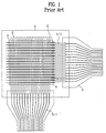
- FIG. 1 is a plan view showing an organic EL display panel to which a related art film type device is attached.
- the organic EL display panel includes a first electrode 2, a second electrode 4, a connecting part 4-1 of the second electrode, a barrier 6 and an organic EL layer 3.
- the strip type electrode is formed by chemically etching on a transparent substrate 1, and the second electrode 4 is formed in perpendicular to the first electrode 2.
- the connecting part 4-1 of the second electrode is used to easily form second electrode patterns, and the barrier is formed to electrically disconnect the second electrode patterns with one another.
- the organic EL layer 3 is deposited on the barrier 6 by a vacuum deposition method.
- the first electrode 2 is formed in perpendicular to the second electrode 4.
- the related art organic EL display panel includes a film type device 5 (COF, FPC, TCP, etc.) having a line 5-1 for connecting the display panel to a driving chip (not shown), and two TAB regions for connecting the display panel to the first and second electrodes.
- COF film type device 5
- FPC FPC
- TCP TCP
- the two film type devices 5 such as FPC, TCP and COF are required to mount the line on the PCB, and the TAB process steps are performed two times.
- manufacturing cost is increased in that the two FPCs (or TCPs) are used and the TAB process steps are performed two times, so that competitive power of the organic EL display panel is weakened due to high manufacturing cost.
- the present invention is directed to an organic EL display panel that substantially obviates one or more problems due to limitations and disadvantages of the related art.
- An object of the present invention is to provide an organic EL display panel, in which a TAB region of a film type device is formed at a minimum size to decrease manufacturing cost of the module, and electrode lines having different lengths are alternately formed in the TAB region to increase a contact region of the electrode lines to connectors in a case of that the pitch of the electrode lines become narrow with high resolution of the organic EL display device, so that it is possible to stably connect the electrode lines to the film type device through the connectors even though an error range for aligning is wide.
- an organic EL display panel includes a driving part; a display panel including a substrate, a plurality of first and second electrodes formed on the substrate in a matrix type, and first and second lines having different lengths for being alternately arranged, and respectively applying signals from the driving part to the first and second electrodes; and a connecting part including a third line for electrically connecting the first and second lines to the driving part.
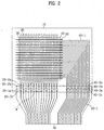
- FIG. 2 is a plan view showing an organic EL display panel to which a film type device according to the present invention is attached.
- the organic EL display panel includes a transparent substrate 10, an organic EL layer 30, a connecting part 40-1 of a second electrode, a barrier 60, first electrode lines 20-2a, 20-2b and second electrode lines 40-2a, 40-2b.
- the organic EL layer 30 is formed in a plurality of pixels defined by crossing a plurality of first and second electrodes 20, 40 to one another.
- the connecting part 40-1 of the second electrode is used for easily forming second electrode patterns, and the barrier 60 is formed to electrically disconnect the second electrodes patterns 40 with one another.
- the first electrode lines 20-2a, 20-2b having different lengths from each other are alternately formed on the transparent substrate 10 for being connected with a first electrode 20.
- the second electrode lines 40-2a, 40-2b having different lengths from each other are alternately formed on the transparent substrate 10 for being connected with the second electrode 40 through the connecting part 40-1 of the second electrode.
- the organic EL display panel further includes first connectors 20-1a, 20-1b connected with the first electrode lines 20-2a, 20-2b, and second connectors 40-1a, 40-1b connected with the second electrode lines 40-2a, 40-2b.
- the first and second electrode lines 20-2a, 20-2b and 40-2a, 40-2b may be formed with transparent electrodes, and supplementary electrodes of metal material for improving conductivity. In another way, the first and second electrode lines may be formed only with the supplementary electrodes.
- the first and second connectors 20-1a, 20-1b and 40-2a, 40-2b are formed with transparent electrodes, and supplementary electrode of metal material for improving conductivity. In another way, the first and second connectors may be formed only with the transparent electrodes.
- the first and second electrode lines 20-2a, 20-2b and 40-2a, 40-2b are arranged in one direction. Then, a film type device 50 (COF, FPC, TCP, etc.) having a line 50-1 of the same pitch with the first and second electrode lines 20-2a, 20-2b and 40-2a, 40-2b is attached to the display panel by a first TAB method.
- COF COF, FPC, TCP, etc.
- the pitch and shape of the line 50-1 of the device 50 is same with that of the first and second electrode lines 20-2a, 20-2b and 40-2a, 40-2b.
- the first and second electrode lines 20-2a, 20-2b and 40-2a, 40-2b are contacted to the line 50-1 of the device 50 by the first TAB method, and the line 50-1 is connected to a driving part (not shown) for driving the organic EL display panel.
- FIG. 3 is a detailed view showing "A" portion of FIG. 2.
- long electrode lines 20-2b, 40-2b and short electrode lines 20-2a, 40-2a are alternately formed in a TAB region B of the organic EL display panel. At this time, the long electrode lines 20-2b, 40-2b formed between the short electrode lines are positioned at a lower part than the short electrode lines.
- the pitch Wp2 between the long electrode lines 20-2b, 40-2b and between the short electrode lines 20-2a, 40-2a is twice as high as the pitch "Wp1" between the electrodes of the display panel.
- wide connectors 20-1a, 20-1b are formed at ends of the electrode lines 20-2a, 20-2b and 40-2a, 40-2b for easily connecting the line of the device to the electrode lines through the connectors.
- the first and second electrodes 20, 40 are directly connected with the line 50-1 of the film type device 50 for driving the display panel by connecting the scan line (first electrode line) to the data line (second electrode line).
- an error range for aligning is narrow, so that the first and second electrode lines could be misaligned with the line 50-1 of the device 50.
- the electrode lines 20-2a, 20-2b and 40-2a, 40-2b having different lengths are alternately arranged, it is possible to increase the width of the connectors 20-1a, 20-1b and 40-1a, 40-1b connected to the electrode lines at a predetermined range, so that the line of the device can be contacted to the connectors within a narrow error range.
- the line 50-1 of the related art device 50 is not within the range of "a" at both sides of the center in the connectors of the first electrode lines 20-2a, 20-2b, the line 50-1 of the device is not contacted to the first electrode 20.
- the error range of the line 50-1 of the device 50 is varied according to the width of the connector 20-1a, 20-1b. That is, if the line 50-1 of the device 50 is within the range of "b" at both sides of the center in the connectors of the first electrode lines 20-2a, 20-2b, the line 50-1 of the device 50 is contacted to the first electrode 20.
- the first electrode lines 20-2a, 20-2b having long and short lengths are alternately formed in the TAB region B of the display panel according to the present invention.
- "2b" which is the width of the first connector 20-1a, 20-1b is wider than "2a” at a range of "x”, which is the width between the first electrodes, to electrically connect the line 50-1 to the first electrode lines 20-2a, 20-2b.
- an insulating layer 70 is formed on the long first electrode line 20-2b between the short first electrode lines 20-2a, so that the long first electrode line 20-2b is insulated from the first connector 20-1a during the TAB process step of the device 50.
- the first electrode line 20-2b is insulated from the connector 20-1a in that the insulating layer 70 is formed on the first electrode line 20-2b.
- the insulating layer 70 is formed of inorganic material such as oxide SiO 2 and nitride SiNx, or organic material such as polyimide (especially, polyacryl, novolac, polyphenyl and polystylene). Also, the insulating layer 70 is formed at a thickness of 0.01 ⁇ m to 10 ⁇ m.
- the structure of the second electrode lines 40-2a, 40-2b and the second connectors 40-1a, 40-1b is same with that of FIG. 3, so that the explanation for the structure will be omitted.
- the organic EL display panel is used for a display device having a film type device such as COF, TCP and FPC.
- the film type device has a driving chip connected to scan and data lines for driving the display panel.
- the display device having the film type device such as COF, TCP and FPC includes the display panel, COF, a plurality of data and scan lines, and a plurality of connecting lines.
- the COF includes a chip part at which the chip is positioned, and a connecting part at which the display panel is positioned.
- the plurality of data and scan lines are connected to the COF from the first and second electrode lines of the display panel.
- the plurality of connecting lines are formed in the connecting part to electrically connect the scan and data lines to the COF, respectively.
- the organic EL display panel according to the present invention has the following advantages.
- the pitch of the electrode line has been decreased.
- the electrode lines having different lengths are alternately formed, it is possible to increase the width of the connector for connecting the electrode line to the line of the device such as COF, FPC and TCP by the TAB method. That is, even though the error range for aligning is wide, the electrode line is stably connected to the line of the device through the connector, so that the reliability of the display panel is obtained, and the yield is improved.
Abstract
Description
- This application claims the benefit of the Korean Application No. 2001-0041891 filed on July 12, 2001, which is hereby incorporated by reference.
- The present invention relates to a display device, and more particularly, to an organic EL display device by a tape automated bonding (TAB) method.
- FIG. 1 is a plan view showing an organic EL display panel to which a related art film type device is attached.
- As shown in FIG. 1, the organic EL display panel includes a
first electrode 2, asecond electrode 4, a connecting part 4-1 of the second electrode, abarrier 6 and anorganic EL layer 3. - The strip type electrode is formed by chemically etching on a
transparent substrate 1, and thesecond electrode 4 is formed in perpendicular to thefirst electrode 2. At this time, the connecting part 4-1 of the second electrode is used to easily form second electrode patterns, and the barrier is formed to electrically disconnect the second electrode patterns with one another. After that, theorganic EL layer 3 is deposited on thebarrier 6 by a vacuum deposition method. - Referring to FIG. 1, the
first electrode 2 is formed in perpendicular to thesecond electrode 4. In this respect, the related art organic EL display panel includes a film type device 5 (COF, FPC, TCP, etc.) having a line 5-1 for connecting the display panel to a driving chip (not shown), and two TAB regions for connecting the display panel to the first and second electrodes. - That is, the two
film type devices 5 such as FPC, TCP and COF are required to mount the line on the PCB, and the TAB process steps are performed two times. - Accordingly, manufacturing cost is increased in that the two FPCs (or TCPs) are used and the TAB process steps are performed two times, so that competitive power of the organic EL display panel is weakened due to high manufacturing cost.
- Accordingly, the present invention is directed to an organic EL display panel that substantially obviates one or more problems due to limitations and disadvantages of the related art.
- An object of the present invention is to provide an organic EL display panel, in which a TAB region of a film type device is formed at a minimum size to decrease manufacturing cost of the module, and electrode lines having different lengths are alternately formed in the TAB region to increase a contact region of the electrode lines to connectors in a case of that the pitch of the electrode lines become narrow with high resolution of the organic EL display device, so that it is possible to stably connect the electrode lines to the film type device through the connectors even though an error range for aligning is wide.
- Additional advantages, objects, and features of the invention will be set forth in part in the description which follows and in part will become apparent to those having ordinary skill in the art upon examination of the following or may be learned from practice of the invention. The objectives and other advantages of the invention may be realized and attained by the structure particularly pointed out in the written description and claims hereof as well as the appended drawings.
- To achieve these objects and other advantages and in accordance with the purpose of the invention, as embodied and broadly described herein, an organic EL display panel according to the present invention includes a driving part; a display panel including a substrate, a plurality of first and second electrodes formed on the substrate in a matrix type, and first and second lines having different lengths for being alternately arranged, and respectively applying signals from the driving part to the first and second electrodes; and a connecting part including a third line for electrically connecting the first and second lines to the driving part.
- It is to be understood that both the foregoing general description and the following detailed description of the present invention are exemplary and explanatory and are intended to provide further explanation of the invention as claimed.
- The accompanying drawings, which are included to provide a further understanding of the invention and are incorporated in and constitute a part of this application, illustrate embodiment(s) of the invention and together with the description serve to explain the principle of the invention. In the drawings:
- FIG. 1 is a plan view showing an organic EL display panel to which a related art film type device is attached;
- FIG. 2 is a plan view showing an organic EL display panel to which a film type device according to the present invention is attached; and
- FIG. 3 is a detailed view showing "A" portion of FIG. 2.
-
- Reference will now be made in detail to the preferred embodiments of the present invention, examples of which are illustrated in the accompanying drawings. Wherever possible, the same reference numbers will be used throughout the drawings to refer to the same or like parts.
- An organic EL display panel according to the present invention will be explained with reference to the accompanying drawings.
- FIG. 2 is a plan view showing an organic EL display panel to which a film type device according to the present invention is attached.
- As shown in FIG. 2, the organic EL display panel includes a
transparent substrate 10, anorganic EL layer 30, a connecting part 40-1 of a second electrode, abarrier 60, first electrode lines 20-2a, 20-2b and second electrode lines 40-2a, 40-2b. - At this time, the
organic EL layer 30 is formed in a plurality of pixels defined by crossing a plurality of first andsecond electrodes barrier 60 is formed to electrically disconnect thesecond electrodes patterns 40 with one another. Also, the first electrode lines 20-2a, 20-2b having different lengths from each other are alternately formed on thetransparent substrate 10 for being connected with afirst electrode 20. The second electrode lines 40-2a, 40-2b having different lengths from each other are alternately formed on thetransparent substrate 10 for being connected with thesecond electrode 40 through the connecting part 40-1 of the second electrode. - The organic EL display panel further includes first connectors 20-1a, 20-1b connected with the first electrode lines 20-2a, 20-2b, and second connectors 40-1a, 40-1b connected with the second electrode lines 40-2a, 40-2b.
- The first and second electrode lines 20-2a, 20-2b and 40-2a, 40-2b may be formed with transparent electrodes, and supplementary electrodes of metal material for improving conductivity. In another way, the first and second electrode lines may be formed only with the supplementary electrodes.
- The first and second connectors 20-1a, 20-1b and 40-2a, 40-2b are formed with transparent electrodes, and supplementary electrode of metal material for improving conductivity. In another way, the first and second connectors may be formed only with the transparent electrodes.
- The first and second electrode lines 20-2a, 20-2b and 40-2a, 40-2b are arranged in one direction. Then, a film type device 50 (COF, FPC, TCP, etc.) having a line 50-1 of the same pitch with the first and second electrode lines 20-2a, 20-2b and 40-2a, 40-2b is attached to the display panel by a first TAB method.
- The pitch and shape of the line 50-1 of the device 50 (FPC, TCP, COF, etc.) is same with that of the first and second electrode lines 20-2a, 20-2b and 40-2a, 40-2b.
- The first and second electrode lines 20-2a, 20-2b and 40-2a, 40-2b are contacted to the line 50-1 of the
device 50 by the first TAB method, and the line 50-1 is connected to a driving part (not shown) for driving the organic EL display panel. - FIG. 3 is a detailed view showing "A" portion of FIG. 2.
- Referring to FIG. 3, long electrode lines 20-2b, 40-2b and short electrode lines 20-2a, 40-2a are alternately formed in a TAB region B of the organic EL display panel. At this time, the long electrode lines 20-2b, 40-2b formed between the short electrode lines are positioned at a lower part than the short electrode lines.
- In this structure, the pitch Wp2 between the long electrode lines 20-2b, 40-2b and between the short electrode lines 20-2a, 40-2a is twice as high as the pitch "Wp1" between the electrodes of the display panel.
- In the TAB region B, wide connectors 20-1a, 20-1b are formed at ends of the electrode lines 20-2a, 20-2b and 40-2a, 40-2b for easily connecting the line of the device to the electrode lines through the connectors.
- Referring to FIG. 3, there is limitation in forming the pitch between the
electrodes - Accordingly, the first and
second electrodes film type device 50 for driving the display panel by connecting the scan line (first electrode line) to the data line (second electrode line). At this time, an error range for aligning is narrow, so that the first and second electrode lines could be misaligned with the line 50-1 of thedevice 50. - However, if the electrode lines 20-2a, 20-2b and 40-2a, 40-2b having different lengths are alternately arranged, it is possible to increase the width of the connectors 20-1a, 20-1b and 40-1a, 40-1b connected to the electrode lines at a predetermined range, so that the line of the device can be contacted to the connectors within a narrow error range.
- For example, if the line 50-1 of the
related art device 50 is not within the range of "a" at both sides of the center in the connectors of the first electrode lines 20-2a, 20-2b, the line 50-1 of the device is not contacted to thefirst electrode 20. - However, in the present invention, the error range of the line 50-1 of the
device 50 is varied according to the width of the connector 20-1a, 20-1b. That is, if the line 50-1 of thedevice 50 is within the range of "b" at both sides of the center in the connectors of the first electrode lines 20-2a, 20-2b, the line 50-1 of thedevice 50 is contacted to thefirst electrode 20. - The first electrode lines 20-2a, 20-2b having long and short lengths are alternately formed in the TAB region B of the display panel according to the present invention. In this respect, "2b" which is the width of the first connector 20-1a, 20-1b is wider than "2a" at a range of "x", which is the width between the first electrodes, to electrically connect the line 50-1 to the first electrode lines 20-2a, 20-2b.
- If the width is increased at the range of "x", it is possible to stably perform the TAB process step even though the error range for aligning is wide.
- Also, an
insulating layer 70 is formed on the long first electrode line 20-2b between the short first electrode lines 20-2a, so that the long first electrode line 20-2b is insulated from the first connector 20-1a during the TAB process step of thedevice 50. - Even though the width of the first connector 20-1a connected to the first electrode line 20-2a is enlarged, the first electrode line 20-2b is insulated from the connector 20-1a in that the
insulating layer 70 is formed on the first electrode line 20-2b. - At this time, the
insulating layer 70 is formed of inorganic material such as oxide SiO2 and nitride SiNx, or organic material such as polyimide (especially, polyacryl, novolac, polyphenyl and polystylene). Also, theinsulating layer 70 is formed at a thickness of 0.01 µm to 10 µm. - The structure of the second electrode lines 40-2a, 40-2b and the second connectors 40-1a, 40-1b is same with that of FIG. 3, so that the explanation for the structure will be omitted.
- The organic EL display panel is used for a display device having a film type device such as COF, TCP and FPC. At this time, the film type device has a driving chip connected to scan and data lines for driving the display panel.
- The display device having the film type device such as COF, TCP and FPC includes the display panel, COF, a plurality of data and scan lines, and a plurality of connecting lines.
- In the display panel, two first electrode lines having different lengths are alternately formed on the transparent substrate, and are connected to the first electrode. Also, two second electrode lines having different lengths are alternately formed in the display panel for being connected with the second electrode. Then, the COF includes a chip part at which the chip is positioned, and a connecting part at which the display panel is positioned. The plurality of data and scan lines are connected to the COF from the first and second electrode lines of the display panel. Subsequently, the plurality of connecting lines are formed in the connecting part to electrically connect the scan and data lines to the COF, respectively.
- As explained above, the organic EL display panel according to the present invention has the following advantages.
- With high resolution of the organic EL display panel, the pitch of the electrode line has been decreased. At this time, if the electrode lines having different lengths are alternately formed, it is possible to increase the width of the connector for connecting the electrode line to the line of the device such as COF, FPC and TCP by the TAB method. That is, even though the error range for aligning is wide, the electrode line is stably connected to the line of the device through the connector, so that the reliability of the display panel is obtained, and the yield is improved.
- Also, it is possible to form the TAB regions at a minimum, so that the cost of the module is decreased in the manufacturing process steps.
- It will be apparent to those skilled in the art that various modifications and variations can be made in the present invention. Thus, it is intended that the present invention covers the modifications and variations of this invention provided they come within the scope of the appended claims and their equivalents.
Claims (8)
- An organic EL display device comprising:a driving part;a display panel including a substrate, a plurality of first and second electrodes formed on the substrate in a matrix type; and first and second lines having different lengths for being alternately arranged, and respectively applying signals from the driving part to the first and second electrodes; anda connecting part including a third line for electrically connecting the first and second lines to the driving part.
- The organic EL display device as claimed in claim 1, further comprising connectors having a predetermined pitch to respectively connect the first and second lines to the third line.
- The organic EL display device as claimed in claim 2, wherein the pitch between the connectors is wider than the pitch between first electrodes, and between second electrodes.
- The organic EL display device as claimed in claim 2 or 3, further comprising an insulating layer formed on the first and second lines, wherein the first and second lines are insulated form the connector by the insulating layer.
- The organic EL display device as claimed in at least one of the preceding claims, further comprising a fourth line connecting the second line having a sectional view of an angle type to the third line, wherein the first and third lines are formed in one direction according to the connection of the second line on the display panel.
- The organic EL display device as claimed in at least one of the preceding claims, wherein the connecting part further comprises a film type device having the third line, wherein the film type device is connected to the display panel by a taped automated bonding (TAB) method.
- The organic EL display device as claimed in claim 6, wherein the film type device is connected to a predetermined region of the display panel having the first electrode line, a connecting line connected to the second electrode line, and the connector connected to the first electrode line and the connecting line by the TAB method.
- The organic EL display device as claimed in at least one of the preceding claims wherein the pitch and the shape of the third line are same with that of the first and second electrode lines.
Priority Applications (1)
| Application Number | Priority Date | Filing Date | Title |
|---|---|---|---|
| EP10183220A EP2261975A1 (en) | 2001-07-12 | 2002-07-05 | Organic EL display device |
Applications Claiming Priority (2)
| Application Number | Priority Date | Filing Date | Title |
|---|---|---|---|
| KR2001041891 | 2001-07-12 | ||
| KR10-2001-0041891A KR100404200B1 (en) | 2001-07-12 | 2001-07-12 | Organic Electroluminescence Display Panel |
Related Child Applications (1)
| Application Number | Title | Priority Date | Filing Date |
|---|---|---|---|
| EP10183220A Division-Into EP2261975A1 (en) | 2001-07-12 | 2002-07-05 | Organic EL display device |
Publications (3)
| Publication Number | Publication Date |
|---|---|
| EP1276154A2 true EP1276154A2 (en) | 2003-01-15 |
| EP1276154A3 EP1276154A3 (en) | 2004-01-28 |
| EP1276154B1 EP1276154B1 (en) | 2012-10-24 |
Family
ID=19712090
Family Applications (2)
| Application Number | Title | Priority Date | Filing Date |
|---|---|---|---|
| EP10183220A Withdrawn EP2261975A1 (en) | 2001-07-12 | 2002-07-05 | Organic EL display device |
| EP02014907A Expired - Fee Related EP1276154B1 (en) | 2001-07-12 | 2002-07-05 | Organic EL display device |
Family Applications Before (1)
| Application Number | Title | Priority Date | Filing Date |
|---|---|---|---|
| EP10183220A Withdrawn EP2261975A1 (en) | 2001-07-12 | 2002-07-05 | Organic EL display device |
Country Status (5)
| Country | Link |
|---|---|
| US (1) | US6710547B2 (en) |
| EP (2) | EP2261975A1 (en) |
| JP (1) | JP3806070B2 (en) |
| KR (1) | KR100404200B1 (en) |
| CN (1) | CN1215558C (en) |
Cited By (5)
| Publication number | Priority date | Publication date | Assignee | Title |
|---|---|---|---|---|
| EP1850390A2 (en) * | 2006-04-28 | 2007-10-31 | LG Electronics Inc. | Display device module |
| CN100379012C (en) * | 2003-06-23 | 2008-04-02 | 铼宝科技股份有限公司 | Organic electroluminescent panel device |
| CN100379013C (en) * | 2003-06-24 | 2008-04-02 | 铼宝科技股份有限公司 | Organic electroluminescent panel device |
| EP2034505A2 (en) * | 2007-09-06 | 2009-03-11 | Samsung SDI Co., Ltd. | Plasma display panel and method of forming electrodes thereof |
| EP2051276A3 (en) * | 2005-04-06 | 2009-10-14 | Samsung SDI Co., Ltd. | Plasma display panel |
Families Citing this family (13)
| Publication number | Priority date | Publication date | Assignee | Title |
|---|---|---|---|---|
| KR100571218B1 (en) * | 2003-07-15 | 2006-04-13 | 엘지전자 주식회사 | Connection member and driving device of plasma display panel |
| US7764012B2 (en) * | 2004-04-16 | 2010-07-27 | Semiconductor Energy Laboratory Co., Ltd | Light emitting device comprising reduced frame portion, manufacturing method with improve productivity thereof, and electronic apparatus |
| JP4439988B2 (en) * | 2004-04-23 | 2010-03-24 | シャープ株式会社 | Display device |
| KR100718963B1 (en) * | 2005-02-17 | 2007-05-16 | 엘지전자 주식회사 | COF/TCP Electrode Unit of Plasma Display Panel |
| KR100927613B1 (en) * | 2005-08-17 | 2009-11-23 | 삼성에스디아이 주식회사 | Plasma display panel |
| KR100637233B1 (en) * | 2005-08-19 | 2006-10-20 | 삼성에스디아이 주식회사 | Plasma display panel |
| JP2008159321A (en) * | 2006-12-21 | 2008-07-10 | Fuji Electric Holdings Co Ltd | Organic el display panel and its manufacturing method |
| TWI472003B (en) * | 2011-08-15 | 2015-02-01 | Au Optronics Corp | Display panel |
| KR20140133106A (en) | 2013-05-09 | 2014-11-19 | 삼성디스플레이 주식회사 | Chip on film including different wiring pattern, flexible display device the same and method of manufactruing of flexible display device |
| CN104319354B (en) * | 2014-11-07 | 2017-01-18 | 京东方科技集团股份有限公司 | Pin binding structure and display panel |
| KR102374713B1 (en) * | 2014-12-18 | 2022-03-15 | 엘지디스플레이 주식회사 | Display panel and organic electroluminescent display appartus having the same |
| CN108630105B (en) * | 2018-05-10 | 2020-06-30 | 京东方科技集团股份有限公司 | Array substrate, display panel and display device |
| KR102581839B1 (en) | 2018-10-02 | 2023-09-22 | 삼성디스플레이 주식회사 | Display device |
Citations (4)
| Publication number | Priority date | Publication date | Assignee | Title |
|---|---|---|---|---|
| EP0767599A2 (en) * | 1995-10-06 | 1997-04-09 | Pioneer Electronic Corporation | Organic electroluminescent display panel and method for manufacturing the same |
| EP0795772A1 (en) * | 1996-03-15 | 1997-09-17 | Canon Kabushiki Kaisha | Drive circuit connection structure and display apparatus including the connection structure |
| JP2000082720A (en) * | 1998-09-07 | 2000-03-21 | Canon Inc | Light emitting device, aligner and image forming apparatus |
| EP1093166A2 (en) * | 1999-10-12 | 2001-04-18 | Sel Semiconductor Energy Laboratory Co., Ltd. | Organic EL display device and method of manufacturing |
Family Cites Families (13)
| Publication number | Priority date | Publication date | Assignee | Title |
|---|---|---|---|---|
| JPS50107890A (en) * | 1974-01-30 | 1975-08-25 | ||
| JPS6154142A (en) * | 1984-08-24 | 1986-03-18 | Nec Corp | Fluorescent character display tube |
| JPH0428145Y2 (en) * | 1987-09-09 | 1992-07-07 | ||
| JPH0730149A (en) * | 1993-07-12 | 1995-01-31 | Nisshin Steel Co Ltd | Light-emitting diode array chip |
| US5684365A (en) * | 1994-12-14 | 1997-11-04 | Eastman Kodak Company | TFT-el display panel using organic electroluminescent media |
| JPH09115673A (en) * | 1995-10-13 | 1997-05-02 | Sony Corp | Light emission element or device, and driving method thereof |
| US6259838B1 (en) * | 1998-10-16 | 2001-07-10 | Sarnoff Corporation | Linearly-addressed light-emitting fiber, and flat panel display employing same |
| KR100473456B1 (en) * | 1998-11-11 | 2005-03-08 | 세이코 엡슨 가부시키가이샤 | Liquid crystal display device |
| JP2001166329A (en) * | 1998-11-11 | 2001-06-22 | Seiko Epson Corp | Liquid crystal display device |
| US6259846B1 (en) * | 1999-02-23 | 2001-07-10 | Sarnoff Corporation | Light-emitting fiber, as for a display |
| JP2000259091A (en) * | 1999-03-04 | 2000-09-22 | Casio Comput Co Ltd | Display panel, flexible wiring board, and display device provided with them |
| JP4472073B2 (en) * | 1999-09-03 | 2010-06-02 | 株式会社半導体エネルギー研究所 | Display device and manufacturing method thereof |
| US6815903B2 (en) * | 2001-12-11 | 2004-11-09 | Seiko Epson Corporation | Display device and electronic apparatus |
-
2001
- 2001-07-12 KR KR10-2001-0041891A patent/KR100404200B1/en active IP Right Grant
-
2002
- 2002-07-05 EP EP10183220A patent/EP2261975A1/en not_active Withdrawn
- 2002-07-05 EP EP02014907A patent/EP1276154B1/en not_active Expired - Fee Related
- 2002-07-10 US US10/191,408 patent/US6710547B2/en not_active Expired - Lifetime
- 2002-07-11 JP JP2002202230A patent/JP3806070B2/en not_active Expired - Fee Related
- 2002-07-12 CN CNB021407118A patent/CN1215558C/en not_active Expired - Fee Related
Patent Citations (4)
| Publication number | Priority date | Publication date | Assignee | Title |
|---|---|---|---|---|
| EP0767599A2 (en) * | 1995-10-06 | 1997-04-09 | Pioneer Electronic Corporation | Organic electroluminescent display panel and method for manufacturing the same |
| EP0795772A1 (en) * | 1996-03-15 | 1997-09-17 | Canon Kabushiki Kaisha | Drive circuit connection structure and display apparatus including the connection structure |
| JP2000082720A (en) * | 1998-09-07 | 2000-03-21 | Canon Inc | Light emitting device, aligner and image forming apparatus |
| EP1093166A2 (en) * | 1999-10-12 | 2001-04-18 | Sel Semiconductor Energy Laboratory Co., Ltd. | Organic EL display device and method of manufacturing |
Non-Patent Citations (1)
| Title |
|---|
| PATENT ABSTRACTS OF JAPAN vol. 2000, no. 06, 22 September 2000 (2000-09-22) -& JP 2000 082720 A (CANON INC), 21 March 2000 (2000-03-21) * |
Cited By (7)
| Publication number | Priority date | Publication date | Assignee | Title |
|---|---|---|---|---|
| CN100379012C (en) * | 2003-06-23 | 2008-04-02 | 铼宝科技股份有限公司 | Organic electroluminescent panel device |
| CN100379013C (en) * | 2003-06-24 | 2008-04-02 | 铼宝科技股份有限公司 | Organic electroluminescent panel device |
| EP2051276A3 (en) * | 2005-04-06 | 2009-10-14 | Samsung SDI Co., Ltd. | Plasma display panel |
| EP1850390A2 (en) * | 2006-04-28 | 2007-10-31 | LG Electronics Inc. | Display device module |
| EP1850390A3 (en) * | 2006-04-28 | 2011-11-30 | LG Display Co., Ltd. | Display device module |
| EP2034505A2 (en) * | 2007-09-06 | 2009-03-11 | Samsung SDI Co., Ltd. | Plasma display panel and method of forming electrodes thereof |
| EP2034505A3 (en) * | 2007-09-06 | 2010-05-19 | Samsung SDI Co., Ltd. | Plasma display panel and method of forming electrodes thereof |
Also Published As
| Publication number | Publication date |
|---|---|
| JP2003045648A (en) | 2003-02-14 |
| US6710547B2 (en) | 2004-03-23 |
| EP2261975A1 (en) | 2010-12-15 |
| JP3806070B2 (en) | 2006-08-09 |
| CN1398145A (en) | 2003-02-19 |
| CN1215558C (en) | 2005-08-17 |
| KR100404200B1 (en) | 2003-11-03 |
| KR20030006202A (en) | 2003-01-23 |
| US20030011318A1 (en) | 2003-01-16 |
| EP1276154B1 (en) | 2012-10-24 |
| EP1276154A3 (en) | 2004-01-28 |
Similar Documents
| Publication | Publication Date | Title |
|---|---|---|
| EP1276154A2 (en) | Organic EL display device | |
| CN109755412B (en) | Flexible substrate, manufacturing method, flexible display device and electronic device | |
| US7630047B2 (en) | Liquid crystal display and method for manufacturing the same | |
| JP4271435B2 (en) | Semiconductor device | |
| KR100689681B1 (en) | Film substrate, manufacturing method thereof and substrate for displaying image | |
| KR100722629B1 (en) | method for packaging flexible substrate and display device thereof | |
| JP4740708B2 (en) | Wiring board and semiconductor device | |
| KR100821433B1 (en) | Display Panel And Display Device | |
| US6603467B1 (en) | Method and apparatus for LCD panel power up test | |
| JP2002328620A (en) | Liquid crystal display | |
| US20050133912A1 (en) | Electrical connection structure | |
| CN108646491B (en) | Display panel and display device using same | |
| KR100309922B1 (en) | A manufacturing method of a liquid crystal display | |
| CN1584717A (en) | Liquid crystal display device | |
| JPH11312715A (en) | Semiconductor device | |
| JP2004205550A (en) | Connecting electrode and picture display device | |
| JP2005227435A (en) | Display device | |
| JPH02205387A (en) | Circuit wiring board device | |
| JPH0732297B2 (en) | Circuit component mounting structure | |
| JP2007036283A (en) | Semiconductor device | |
| JP2001142084A (en) | Liquid crystal panel and method of producing the same |
Legal Events
| Date | Code | Title | Description |
|---|---|---|---|
| PUAI | Public reference made under article 153(3) epc to a published international application that has entered the european phase |
Free format text: ORIGINAL CODE: 0009012 |
|
| AK | Designated contracting states |
Kind code of ref document: A2 Designated state(s): AT BE BG CH CY CZ DE DK EE ES FI FR GB GR IE IT LI LU MC NL PT SE SK TR |
|
| AX | Request for extension of the european patent |
Free format text: AL;LT;LV;MK;RO;SI |
|
| PUAL | Search report despatched |
Free format text: ORIGINAL CODE: 0009013 |
|
| AK | Designated contracting states |
Kind code of ref document: A3 Designated state(s): AT BE BG CH CY CZ DE DK EE ES FI FR GB GR IE IT LI LU MC NL PT SE SK TR |
|
| AX | Request for extension of the european patent |
Extension state: AL LT LV MK RO SI |
|
| 17P | Request for examination filed |
Effective date: 20040503 |
|
| AKX | Designation fees paid |
Designated state(s): DE FR GB NL |
|
| REG | Reference to a national code |
Ref country code: DE Ref legal event code: R079 Ref document number: 60243903 Country of ref document: DE Free format text: PREVIOUS MAIN CLASS: H01L0027000000 Ipc: H01L0027320000 |
|
| RIC1 | Information provided on ipc code assigned before grant |
Ipc: H01L 27/32 20060101AFI20120227BHEP |
|
| GRAP | Despatch of communication of intention to grant a patent |
Free format text: ORIGINAL CODE: EPIDOSNIGR1 |
|
| GRAS | Grant fee paid |
Free format text: ORIGINAL CODE: EPIDOSNIGR3 |
|
| GRAA | (expected) grant |
Free format text: ORIGINAL CODE: 0009210 |
|
| AK | Designated contracting states |
Kind code of ref document: B1 Designated state(s): DE FR GB NL |
|
| REG | Reference to a national code |
Ref country code: GB Ref legal event code: FG4D |
|
| REG | Reference to a national code |
Ref country code: DE Ref legal event code: R096 Ref document number: 60243903 Country of ref document: DE Effective date: 20121220 |
|
| REG | Reference to a national code |
Ref country code: NL Ref legal event code: T3 |
|
| PLBE | No opposition filed within time limit |
Free format text: ORIGINAL CODE: 0009261 |
|
| STAA | Information on the status of an ep patent application or granted ep patent |
Free format text: STATUS: NO OPPOSITION FILED WITHIN TIME LIMIT |
|
| 26N | No opposition filed |
Effective date: 20130725 |
|
| REG | Reference to a national code |
Ref country code: DE Ref legal event code: R097 Ref document number: 60243903 Country of ref document: DE Effective date: 20130725 |
|
| GBPC | Gb: european patent ceased through non-payment of renewal fee |
Effective date: 20130705 |
|
| REG | Reference to a national code |
Ref country code: FR Ref legal event code: ST Effective date: 20140331 |
|
| PG25 | Lapsed in a contracting state [announced via postgrant information from national office to epo] |
Ref country code: GB Free format text: LAPSE BECAUSE OF NON-PAYMENT OF DUE FEES Effective date: 20130705 |
|
| PG25 | Lapsed in a contracting state [announced via postgrant information from national office to epo] |
Ref country code: FR Free format text: LAPSE BECAUSE OF NON-PAYMENT OF DUE FEES Effective date: 20130731 |
|
| PGFP | Annual fee paid to national office [announced via postgrant information from national office to epo] |
Ref country code: NL Payment date: 20200608 Year of fee payment: 19 |
|
| PGFP | Annual fee paid to national office [announced via postgrant information from national office to epo] |
Ref country code: DE Payment date: 20200605 Year of fee payment: 19 |
|
| REG | Reference to a national code |
Ref country code: DE Ref legal event code: R119 Ref document number: 60243903 Country of ref document: DE |
|
| REG | Reference to a national code |
Ref country code: NL Ref legal event code: MM Effective date: 20210801 |
|
| PG25 | Lapsed in a contracting state [announced via postgrant information from national office to epo] |
Ref country code: DE Free format text: LAPSE BECAUSE OF NON-PAYMENT OF DUE FEES Effective date: 20220201 |
|
| PG25 | Lapsed in a contracting state [announced via postgrant information from national office to epo] |
Ref country code: NL Free format text: LAPSE BECAUSE OF NON-PAYMENT OF DUE FEES Effective date: 20210801 |