EP1296332A2 - Magnetic memory device - Google Patents
Magnetic memory device Download PDFInfo
- Publication number
- EP1296332A2 EP1296332A2 EP02256086A EP02256086A EP1296332A2 EP 1296332 A2 EP1296332 A2 EP 1296332A2 EP 02256086 A EP02256086 A EP 02256086A EP 02256086 A EP02256086 A EP 02256086A EP 1296332 A2 EP1296332 A2 EP 1296332A2
- Authority
- EP
- European Patent Office
- Prior art keywords
- layer
- read
- conductor
- line
- lines
- Prior art date
- Legal status (The legal status is an assumption and is not a legal conclusion. Google has not performed a legal analysis and makes no representation as to the accuracy of the status listed.)
- Granted
Links
Images


Classifications
-
- G—PHYSICS
- G11—INFORMATION STORAGE
- G11C—STATIC STORES
- G11C11/00—Digital stores characterised by the use of particular electric or magnetic storage elements; Storage elements therefor
- G11C11/02—Digital stores characterised by the use of particular electric or magnetic storage elements; Storage elements therefor using magnetic elements
- G11C11/14—Digital stores characterised by the use of particular electric or magnetic storage elements; Storage elements therefor using magnetic elements using thin-film elements
- G11C11/15—Digital stores characterised by the use of particular electric or magnetic storage elements; Storage elements therefor using magnetic elements using thin-film elements using multiple magnetic layers
-
- G—PHYSICS
- G11—INFORMATION STORAGE
- G11C—STATIC STORES
- G11C11/00—Digital stores characterised by the use of particular electric or magnetic storage elements; Storage elements therefor
- G11C11/02—Digital stores characterised by the use of particular electric or magnetic storage elements; Storage elements therefor using magnetic elements
- G11C11/16—Digital stores characterised by the use of particular electric or magnetic storage elements; Storage elements therefor using magnetic elements using elements in which the storage effect is based on magnetic spin effect
-
- B—PERFORMING OPERATIONS; TRANSPORTING
- B82—NANOTECHNOLOGY
- B82Y—SPECIFIC USES OR APPLICATIONS OF NANOSTRUCTURES; MEASUREMENT OR ANALYSIS OF NANOSTRUCTURES; MANUFACTURE OR TREATMENT OF NANOSTRUCTURES
- B82Y10/00—Nanotechnology for information processing, storage or transmission, e.g. quantum computing or single electron logic
-
- G—PHYSICS
- G11—INFORMATION STORAGE
- G11C—STATIC STORES
- G11C11/00—Digital stores characterised by the use of particular electric or magnetic storage elements; Storage elements therefor
- G11C11/02—Digital stores characterised by the use of particular electric or magnetic storage elements; Storage elements therefor using magnetic elements
- G11C11/16—Digital stores characterised by the use of particular electric or magnetic storage elements; Storage elements therefor using magnetic elements using elements in which the storage effect is based on magnetic spin effect
- G11C11/165—Auxiliary circuits
- G11C11/1653—Address circuits or decoders
- G11C11/1655—Bit-line or column circuits
-
- G—PHYSICS
- G11—INFORMATION STORAGE
- G11C—STATIC STORES
- G11C11/00—Digital stores characterised by the use of particular electric or magnetic storage elements; Storage elements therefor
- G11C11/02—Digital stores characterised by the use of particular electric or magnetic storage elements; Storage elements therefor using magnetic elements
- G11C11/16—Digital stores characterised by the use of particular electric or magnetic storage elements; Storage elements therefor using magnetic elements using elements in which the storage effect is based on magnetic spin effect
- G11C11/165—Auxiliary circuits
- G11C11/1673—Reading or sensing circuits or methods
-
- H—ELECTRICITY
- H10—SEMICONDUCTOR DEVICES; ELECTRIC SOLID-STATE DEVICES NOT OTHERWISE PROVIDED FOR
- H10B—ELECTRONIC MEMORY DEVICES
- H10B61/00—Magnetic memory devices, e.g. magnetoresistive RAM [MRAM] devices
Definitions
- the read lines 22 are electrically insulated from the bit lines 20, they do not add to the resistive cross coupling of the magnetic tunnel junctions 11. Therefore, an equal potential is not applied to the read lines 22.
Abstract
Description
- The present invention relates to magneto-resistive devices and to data storage.
- Magnetic Random Access Memory ("MRAM") is a non-volatile memory that is being considered for short-term and long-term data storage. MRAM has lower power consumption than short-term memory such as DRAM, SRAM and Flash memory. MRAM can perform read and write operations much faster (by orders of magnitude) than conventional long-term storage devices such as hard drives. In addition, MRAM is more compact and consumes less power than hard drives. MRAM is also being considered for embedded applications such as extremely fast processors and network appliances.
- A typical MRAM device includes an array of memory cells, word lines extending along rows of the memory cells, and bit lines extending along columns of the memory cells. Each memory cell is located at a cross point of a word line and a bit line.
- The memory cells may be based on tunneling magneto-resistive (TMR) devices such as spin dependent tunneling (SDT) junctions. A typical SDT junction includes a pinned layer, a sense layer and an insulating tunnel barrier sandwiched between the pinned and sense layers. The pinned layer has a magnetization orientation that is fixed so as not to rotate in the presence of an applied magnetic field in a range of interest. The sense layer has a magnetization that can be oriented in either of two directions: the same direction as the pinned layer magnetization or the opposite direction of the pinned layer magnetization. If the magnetizations of the pinned and sense layers are in the same direction, the orientation of the SDT junction is said to be "parallel." If the magnetizations of the pinned and sense layers are in opposite directions, the orientation of the SDT junction is said to be "anti-parallel." These two stable orientations, parallel and anti-parallel, may correspond to logic values of '0' and '1.'
- The magnetization orientation of the pinned layer may be fixed by an underlying antiferromagnetic (AF) pinning layer. The AF pinning layer provides a large exchange field, which holds the magnetization of the pinned layer in one direction. Underlying the AF layer are usually first and second seed layers. The first seed layer allows the second seed layer to be grown with a (111) crystal structure orientation. The second seed layer establishes a (111) crystal structure orientation for the AF pinning layer.
- The present invention seeks to provide an improved memory device.
- A memory device according to the present invention includes a data ferromagnetic layer having a magnetization that can be oriented in either of two directions, a reference layer, and a spacer layer between the data and reference layers. The reference layer includes a dielectric layer, first and second conductors separated by the dielectric layer, and a ferromagnetic cladding on the first and second conductors. The memory device may be read by temporarily setting the magnetization of the reference layer to a known orientation, and determining a resistance state of the device.
- Embodiments of the present invention are described below, by way of example only, with reference to the accompanying drawings in which:
- Figure 1 is an illustration of an embodiment of magnetic memory device.
- Figure 2 is an illustration of hysteresis loops for data and reference layers of the magnetic memory device shown in Figure 1.
- Figure 3 is an illustration of a first method of performing a read operation on the magnetic memory device shown in Figure 1.
- Figures 4a and 4b are illustrations of device magnetization orientations corresponding to the first method.
- Figure 5 is an illustration of a second method of performing a read operation on the memory device shown in Figure 1.
- Figure 6a-6e and 7a-7e further illustrate the second method.
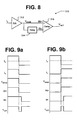
- Figure 8 is an illustration of a circuit for implementing the second method.
- Figures 9a and 9b are timing diagrams for the circuit shown in Figure 8.
- Figure 10 is an illustration of an embodiment of MRAM device.
- Figure 11 is an illustration of another embodiment of MRAM device.
- Figure 12 is an illustration of the alternative MRAM device during a read operation.
- Figures 13a, 13b and 14-17 are illustrations of different embodiments of clad conductors for an MRAM device.
- Figures 18-21 illustrate an embodiment of fabrication of clad conductors.
-
- Referring to Figure 1, a
magnetic memory device 10 includes amagnetic tunnel junction 11 having adata layer 12, areference layer 14, and aninsulating tunnel barrier 16 between the data andreference layers layers data layer 12 has a magnetization (represented by the vector M1) that can be oriented in either of two directions, typically along the easy axis (EA1) of thedata layer 12. Thereference layer 14 has a magnetization (represented by the vector M2) that can be oriented in either of two directions, typically along its easy axis (EA2). The easy axes (EA1, EA2) are shown as extending along the x-axis. - If the magnetizations vectors (M1 and M2) of the data and
reference layers magnetic tunnel junction 11 is said to be "parallel." If the magnetization vectors (M1 and M2) of the data andreference layers magnetic tunnel junction 11 is said to be "anti-parallel. " These two stable orientations, parallel and anti-parallel, may correspond to logic values of '0' and '1.' - The
insulating tunnel barrier 16 allows quantum mechanical tunneling to occur between the data andreference layers magnetic tunnel junction 11 to be a function of the relative orientations of the magnetization vectors (M1 and M2) of the data andreference layers magnetic tunnel junction 11 is a first value (R) if the magnetization orientation of themagnetic tunnel junction 11 is parallel and a second value (R+ΔR) if the magnetization orientation is anti-parallel. Theinsulating tunnel barrier 16 may be made of aluminum oxide (Al2O3), silicon dioxide (SiO2), tantalum oxide (Ta2O5), silicon nitride (SiN4), aluminum nitride (AlNx), or magnesium oxide (MgO). Other dielectrics and certain semiconductor materials may be used for theinsulating tunnel barrier 16. Thickness of theinsulating tunnel barrier 16 may range from about 0.5 nanometers to about three nanometers. - Coercivity (HC1) of the
data layer 12 is much higher than coercivity (HC2) of the reference layer 14 (see Figure 2, which shows hysteresis loops L1 and L2 for the data andreference layers data layer 12 may be at least 2-5 times greater than the coercivity of thereference layer 14. For example, the coercivity (HC1) of thedata layer 12 may be about 25 Oe, and the coercivity (HC2) of thereference layer 14 may be about 5 Oe. It is preferred to make the coercivity (HC2) of thereference layer 14 as low as possible (e.g., by making thereference layer 14 as thin as possible). Thus, thereference layer 14 is considered "softer" than thedata layer 12 because its magnetization vector (M2) is much easier to flip. - Coercivities of the two
layers layers data layer 12 may be made of a material such as NiFeCo or CoFe, and thereference layer 14 may be made of a material such as NiFe. - A
first conductor 18 extending along the x-axis is in contact with thedata layer 12. Asecond conductor 20 extending along the y-axis is in contact with thereference layer 14. The first andsecond conductors second conductor 20 is athird conductor 22, which also extends along the y-axis. An electrical insulator 24 (e.g., a layer of dielectric material) separates the second andthird conductors conductors - Data may be written to the
magnetic tunnel junction 11 by supplying write currents to the first andsecond conductors first conductor 18 creates a magnetic field about thefirst conductor 18, and the current supplied to thesecond conductor 20 creates a magnetic field about thesecond conductor 20. The two magnetic fields, when combined, exceed the coercivity (HC1) of thedata layer 12 and, therefore, cause the magnetization vector (M1) of thedata layer 12 to be set in a desired orientation (the orientation will depend upon the directions of the currents supplied to the first andsecond conductors 18 and 20). The magnetization will be set to either the orientation that corresponds to a logic '1' or the orientation that corresponds to a logic '0'. Because the coercivity (HC2) of thereference layer 14 is less than that of thedata layer 12, the combined magnetic fields cause magnetization (M2) of thereference layer 14 to assume that same orientation as the magnetization (M1) as thedata layer 12. - After write currents are removed from the
conductors data layer 12 retains its orientation. The magnetization vector (M2) of thereference layer 14 may or may not retain its orientation. If thereference layer 14 is "ultra-soft," it will lose its magnetization orientation when the write currents are removed from the first andsecond conductors - The
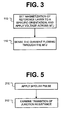
third conductor 22 may be used to assist with write operations. By supplying a current to thethird conductor 22 during write operations, the resulting magnetic field about thethird conductor 22 combines with the other two magnetic fields to help set the magnetization vector (M1) of thedata layer 12 in the desired orientation. - Figure 3 illustrates a first method of reading the
magnetic memory device 10. A current is supplied to thethird conductor 22, and the resulting magnetic field causes the magnetization vector (M2) of thereference layer 14 to assume a specific orientation (block 110). The resulting magnetic field does not affect the magnetization vector (M1) of thedata layer 12. Since the coercivity (Hc2) of thereference layer 14 is low, the magnitude of the third conductor current may be low. - As the current is supplied to the
third conductor 22, a voltage is applied across the magnetic tunnel junction 11 (block 110). The first andsecond conductors magnetic tunnel junction 11. The voltage causes a sense current to flow through themagnetic tunnel junction 11. - The resistance of the
magnetic tunnel junction 11 is measured by sensing the current flowing though the magnetic tunnel junction 11 (block 112). The sensed current is inversely proportional to the resistance of themagnetic tunnel junction 11. Thus Is = V/R or Is =V/(R+ΔR), where V is the applied voltage, Is is the sensed current, R is the nominal resistance of thedevice 10, and ΔR is the change in resistance caused by going from a parallel magnetization orientation to an anti-parallel magnetization orientation - Reference is now made to Figures 4a and 4b. Consider a
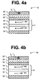
magnetic tunnel junction 11 having a nominal resistance (R) of 1 Mohm, and a tunneling magneto-resistance of 30%. A read current (IR) is depicted as flowing into thethird conductor 22. The read current (IR) causes the magnetization vector (M2) of thereference layer 14 to point to the left. If the measured resistance R=1 Mohm, thedata layer 12 stores a first logic value (Figure 4a). If the measured resistance R= 1.3 Mohm, the data layer stores a second logic value (Figure 4b). Thus, by setting the magnetization of thereference layer 14 to a known orientation and measuring the resistance of the device 10 (either R or R+ΔR), the logic value stored in themagnetic memory device 10 is determined. - Figure 5 illustrates a second method of reading the
magnetic memory device 10. A bipolar pulse is applied to the third conductor 22 (block 210), and transition of junction resistance is examined (212). The direction of the transition (that is, going from high to low, or low to high) indicates the magnetization orientation of thedata layer 12 and, therefore, the logic value stored in themagnetic memory device 10. - Figures 6a-6e further illustrate the second method in connection with a
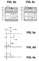
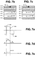
data layer 12 that stores a logic '0.' Abipolar pulse 250 is applied to the third conductor 22 (Figure 6a). Thebipolar pulse 250 has a positive polarity 252 (corresponding to a logic '0') followed by a negative polarity 254 (corresponding to a logic '1'). Thepositive polarity 252 orients the magnetization of thereference layer 14 in the same direction as that of the data layer 12 (Figure 6b), whereby the magnetization orientation of thedevice 10 is parallel and its resistance value is Rp. Then thenegative polarity 254 orients the magnetization vector (M2) of thereference layer 14 in the opposite direction (Figure 6c), whereby the magnetization orientation of thedevice 10 is anti-parallel and its resistance value is R+ΔR or Rap. Thus the resistance of thedevice 10 transitions from low to high (Figure 6d). The low-to-high transition indicates that a logic '0' is stored in thememory device 10. The corresponding sense current (IS) is shown in Figure 6e. - Figures 7a-7e illustrate the second method in connection with a
data layer 12 that stores a logic '1.' The samebipolar pulse 250 is applied to the third conductor 22 (Figure 7a). The magnetic memory device transitions from an anti-parallel magnetization orientation (Figure 7b) to a parallel magnetization orientation (Figure 7c), whereby the resistance of themagnetic memory device 10 transitions from high to low (Figure 7d). Thus the high-to-low transition indicates that a logic '1' is stored in themagnetic memory device 10. The corresponding sense current (IS) is shown in Figure 7e. - The bipolar read operation references to itself. Therefore, this dynamic approach is insensitive to resistance variations across different devices.
- The bipolar pulse is not limited to a single positive polarity followed by a single negative polarity, nor is it limited to a positive polarity that corresponds to a logic '0' and a negative polarity that corresponds to a logic '1'. For example, a positive polarity could just as easily correspond to a logic '1', a bipolar pulse could begin with a negative polarity and transition to a positive polarity, etc.
- A
simple sense amplifier 310 for detecting the resistance transition is shown in Figure 8. The sense current (IS) flowing through themagnetic tunnel junction 11 is supplied to asense amplifier 312. First and second outputs of thesense amplifier 312 provide a voltage (VSENSE) that is proportional to sense current magnitude. The first output is supplied to a first input (IN+) of acomparator 316. The second output of thesense amplifier 312 is supplied to adelay element 314, which has a delay of several nanoseconds. An output of thedelay element 314 is supplied to a second input (IN-) of thecomparator 316. Thecomparator 316 compares the sense voltage (VSENSE) at the first comparator input (IN+) to the delayed sense voltage at the second comparator input (IN-). An output (VOUT) of thecomparator 316 indicates the logic state stored in themagnetic memory device 10. - Figures 9a and 9b are timing diagrams for the circuit of Figure 8. Figure 9a corresponds to Figures 6a-6e, and Figure 9b corresponds to Figures 7a-7e.
- The
magnetic memory device 10 has a simpler structure than a conventional SDT junction. Themagnetic memory device 10 is simpler to fabricate than an SDT junction because seed layers and an AF pinning layer are not needed. Annealing of the data layer to set the easy axis may still be performed, but it is done at lower temperatures and is less critical. In addition, the complexity of the deposition process is significantly reduced. Another advantage is that thedata layer 12 is on top of a metal conductor, resulting in a more uniform data film and, therefore, better magnetic response and manufacturability (in terms of greater uniformity over a wafer). - Reference is now made to Figure 10, which illustrates an
MRAM device 410 including anarray 12 ofmagnetic tunnel junctions 11. Themagnetic tunnel junctions 11 are arranged in rows and columns, with the rows extending along an x-direction and the columns extending along a y-direction. Only a relatively small number of themagnetic tunnel junctions 11 is shown to simplify the illustration of theMRAM device 410. In practice, arrays of any size may be used. - Traces functioning as word lines 18 extend along the x-direction in a plane on one side of the
array 12. The word lines 18 are in contact with the data layers 12 of themagnetic tunnel junctions 11. Traces functioning asbit lines 20 extend along the y-direction in a plane on an adjacent side of thearray 12. The bit lines 20 are in contact with the reference layers 14 of themagnetic tunnel junctions 11. There may be oneword line 18 for each row of thearray 12 and onebit line 20 for each column of thearray 12. Each magneticmemory tunnel junction 11 is located at a cross point of aword line 18 and abit line 20. - Traces functioning as read
lines 22 also extend along the y-direction. The read lines 22 are on top of, and insulated from, the bit lines 20. (In the alternative, theread lines 22 may be beneath the bit lines 20, on top of or beneath the word lines 18, along rows or columns, etc.) The read lines 22 are independent of the word andbit lines - The
MRAM device 410 also includes first andsecond row decoders second column decoders write circuit 418. The read/write circuit 418 includes asense amplifier 420,ground connections 422, a rowcurrent source 424, avoltage source 426, and a columncurrent source 428. - During a write operation on a selected
magnetic tunnel junction 11, thefirst row decoder 414a connects one end of a selectedword line 18 to the rowcurrent source 424, thesecond row decoder 414b connects an opposite end of the selectedword line 18 to ground, thefirst column decoder 416a connects one end of a selectedbit line 20 to ground, and thesecond column decoder 416b connects the opposite end of the selectedbit line 20 to the columncurrent source 428. As a result, write currents flow through the selected word andbit lines magnetic tunnel junction 11 to switch. Thecolumn decoders line 22 crossing the selectedmagnetic tunnel junction 11. This third write current creates an additional magnetic field that assists in switching the selectedmagnetic tunnel junction 11. - During a read operation on a selected
magnetic tunnel junction 11, thefirst row decoder 414a connects thevoltage source 426 to a selectedword line 18, and thefirst column decoder 416a connects a selectedbit line 20 to a virtual ground input of thesense amplifier 420. As a result, a sense current flows through the selectedmagnetic tunnel junction 11 to the input of thesense amplifier 420. In the meantime, the first andsecond column decoders line 22 crossing the selectedmagnetic tunnel junction 11. If a steady read current is supplied to the selected readline 22, the resistance state of the selectedmagnetic tunnel junction 11 is sensed by thesense amplifier 420. If a bipolar pulse is supplied to the selected readline 22, the transition of the junction resistance is examined by the sense amplifier 420 (asense amplifier 420 for examining the transition of the junction resistance may have the same configuration as thesense amplifier 312 shown in Figure 8). - The
magnetic tunnel junctions 11 are coupled together through many parallel paths. The resistance seen at one cross point equals the resistance of themagnetic tunnel junction 11 at that cross point in parallel with resistances ofmagnetic tunnel junctions 11 in the other rows and columns. Thus thearray 12 ofmagnetic tunnel junctions 11 may be characterized as a cross point resistor network. - As the
magnetic tunnel junctions 11 are connected as a cross point resistor network, parasitic or sneak path currents can interfere with the read operations on selectedmagnetic tunnel junctions 11. Blocking devices such as diodes or transistors may be connected to themagnetic tunnel junctions 11. These blocking devices can block the parasitic currents. - In the alternative, the parasitic currents may be dealt with by using an "equipotential" method disclosed in assignee's U.S. Patent No. 6,259,644. If configured to use the equipotential method, the read/
write circuit 418 may provide the same potential to theunselected bit lines 20 as the selectedbit line 20, or it may provide the same potential to the unselected word lines 18 as the selectedbit line 20. - As the read
lines 22 are electrically insulated from the bit lines 20, they do not add to the resistive cross coupling of themagnetic tunnel junctions 11. Therefore, an equal potential is not applied to the read lines 22. - Figure 10 shows an
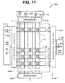
MRAM device 410 with three different types of traces: word lines 18,bit lines 20, and readlines 22. However, the present invention is not so limited. For example, an MRAM device according to the present invention may have only two different types of traces: word lines 18 and bit lines 20. - Reference is made to Figure 11, which illustrates an
MRAM device 510 includingword lines 18 andbit lines 20, but not read lines 22.Magnetic tunnel junctions 11 are located at cross points of word andbit lines - Additional reference is made to Figure 12, which illustrates a read operation using only the word and
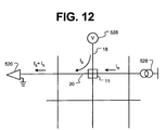
bit lines first row decoder 514a connects thevoltage source 526 to a selectedword line 18, and thefirst column decoder 516a connects one end of a selectedbit line 20 to a virtual ground input of thesense amplifier 520. As a result, a sense current (IS) flows through the selectedmagnetic tunnel junction 11 to thesense amplifier 520. Thesecond column decoder 516b connects the columncurrent source 528 to the other end of the selectedbit line 20. As a result, a read current (IR) flows through the selectedbit line 20 to thesense amplifier 520. The read current (IR) sets the magnetization vector of the reference layer. Thesense amplifier 520 senses the sum of sense and read currents (IS+IR). Since the magnitude of the read current (IR) is known, the magnitude of the sense current (IS), and hence the resistance and logic states of themagnetic tunnel junction 11, can be determined. - The
magnetic tunnel junctions 11 described thus far include individual reference layers 14, with eachreference layer 14 having the same geometry as its correspondingdata layer 12 andtunnel barrier 16. However, the present invention is not limited to reference layers having the same geometry as the data layers and tunnel barriers. - Instead, the reference layers may have the same geometry as the word and
bit lines - Reference is now made to Figure 13a, which shows a
reference line 610 that is shared by multiplemagnetic tunnel junctions 611. Layered on top of thereference line 610 are bit and readlines reference line 610 extends in the same direction as the bit and readlines magnetic tunnel junction 611 of a column includes anindividual data layer 12, anindividual tunnel barrier 16, and the sharedreference line 610. - The present invention is not limited to
reference lines 610 that are layered beneathbit lines 20 as shown in Figure 13a. Instead, thereference lines 610 may be layered on top of bit lines 20 (see Figure 13b); or thereference lines 610 may be layered on or beneath read lines 22 (and would extend in the same direction as the read lines 22), or thereference lines 610 may be layered on or beneath word lines 18 (and would extend in the same direction as the word lines 18). If thereference line 610 is layered on top of thebit line 20 and, therefore, is not in contact with thetunnel barrier 16, than a patternedlayer 14 is formed between thetunnel barrier 16 and the word,bit line 20, as shown in Figure 13b. - The present invention is not limited to reference lines that are layered with respect to word, bit or read
lines - Figure 14 shows a
bit line 20 that is clad with a ferromagnetic material (e.g., NiFe). Thecladding 712 forms a soft orultra-soft reference line 710. Thebit line 20 is located between the readline 22 and the insulatingtunnel barrier 16. A dielectric layer (not shown) may separate the readline 22 from thereference line 710. - The
ferromagnetic cladding 712 may completely enclose thebit line 20 to provide flux path closure. That portion of thecladding 712 between thetunnel barrier 16 and thebit line 20 may be thinner. - During write operations, a write current is applied to the
bit line 20 and the resulting magnetic field causes thereference line 710 to saturate. The thinner portion of thereference line 710 directs the magnetic field to thedata layer 12. - During read operations, a read current flows through the read
line 22 to set the magnetization orientation of thereference line 710, while sense and parasitic currents flow through the word and bit lines. Theferromagnetic cladding 712 should not saturate in the presence of magnetic field created by sense and parasitic currents flowing through the word lines during read operations. As long as it does not, any magnetic fields arising from sense and parasitic currents will not interfere with thedata layer 12. - Figure 15 shows a
read line 22 that is clad with a ferromagnetic material (e.g., NiFe). The cladding forms a soft orultra-soft reference line 810. The readline 22 is located between theword line 20 and the insulatingtunnel barriers 16. The ferromagnetic cladding may completely enclose the readline 22 to provide flux path closure (as shown in Figure 16), or it may partially surround the read line 22 (not shown). The unclad portion of such aread line 22 is in direct contact with thetunnel barriers 16, and the remaining portions are clad with ferromagnetic material. - The
ferromagnetic cladding 812 should not saturate in the presence of a read magnetic field (that is, the magnetic field that occurs when a read current is supplied to the readline 22 and that is used to orient the magnetization vector of the reference line 810). As long as thecladding 812 fully contains the read magnetic field, the read magnetic field will not extend beyond thecladding 812, where it could interfere with thedata layer 12. - As compared to the configuration of Figure 14, the
word line 20 is moved further away from thedata layer 12, which reduces the strength of the magnetic field applied by theword line 20 during write operations. To compensate for the reduced magnetic field, a write current is also supplied to theclad read line 810 during write operations. The magnetic field provided by the readline 22 during write operations assists with switching. - Figure 16 shows a
reference line 912 including ferromagnetic material that is clad onto both abit line 20 and a readline 22. Thereference line 912 includes three portions: alower portion 912a, anupper portion 912b, and acap portion 912c. Thelower portion 912a is separated from the other twoportions other portions lower portion 912a is magnetically coupled to theother portions - The
lower portion 912a of thereference line 912 includes the readline 22. Cladding covers the bottom and sides of the readline 22. The upper surface of the readline 22 is not covered with ferromagnetic cladding, but is covered with the dielectric 914. - The
upper portion 912b of thereference line 912 includes thebit line 20. Cladding covers the top and sides of thebit line 20. The bottom surface of thebit line 20 is not covered with cladding, but is covered with the dielectric 914. The bit and readlines - The read
line 22 is provided with a larger cross-section than thebit line 20 to compensate for manufacturing tolerances. During manufacture, the upper portion of thereference line 912b should be centered over thelower portion 912a. In practice, however, misalignments can occur. Even if misalignments occur, the upper portion will still be positioned over thelower portion 912a so as not to cause a short between the bit and readlines - The
cap portion 912c extends outward from theupper portion 912b and over the sidewalls of thelower portion 912a. Thecap portion 912c also covers the dielectric 914. Thecap portion 912c closes the magnetic flux path between the lower andupper portions cap portion 912c and sidewalls of thelower portion 912a may be filled with the dielectric 914. The gap prevents a short between thebit line 20 and the readline 22. The magnetic field produced by thebit line 20 extends across the gap and into thecap portion 912c. - A plurality of insulating
tunnel barriers 16 are formed on theupper portion 912b of thereference line 912, and corresponding data layers 12 are formed on the insulatingtunnel barriers 16.Word lines 18 are formed on the data layers 12. - The depiction of the cladding thickness in the
lower portion 912a is exaggerated. The thickness may be about 1 nm to 50 nm (with a typical value of 5 nm) for the lower, upper, andcap portions line 22 does not saturate theupper portion 912b of thereference line 912. A write magnetic field produced only by thebit line 20 can saturate thelower portion 912a of thereference line 912. - The electrical insulation (i.e., the dielectric 914) between the bit and read
lines lines lines lower portion 912a only, or the magnetization of theupper portion 912b only, or the magnetization of both the upper andlower portions reference line 912. - Figure 17 shows a reference line 912' in which the sidewalls of the
lower portion 912a' extend upward above the dielectric layer 914'. There is an air gap or insulator between the sides of thecap portion 912c' and sidewalls of thelower portion 912a'. - A Cu-demascene process may be used to fabricate the clad conductors. An exemplary Cu-demascene process is illustrated in Figures 18-21.
- The process begins with a planarized dielectric layer 101 in which a trench has been etched prior to interconnect metal deposition (Figure 18). A thin layer of soft
magnetic material 912a is deposited with an isotropic process so that the side walls are coated to roughly the same thickness as the bottom of the trench (Figure 19). The magnetic material is permeable enough to act as a magnetic core, and it is continuous all around in cross-sections without any breaks or too many voids. The trench is then filled withcopper 22 by electroplating or other suitable means. The structure is then planarized. Resulting is the planarized structure shown in Figure 20. A softmagnetic material 912c is deposited to close the flux path and form the wholly-clad conductor (Figure 21). The magnetic properties may be manipulated as desired by making the thickness of thecap portion material 912c different than the thickness of thematerial 912a covering the sidewalls and bottom of the trench. Thiscap portion 912c is patterned and then the remainder of the clad conductor is fabricated. - The present invention is not limited to a demascene process for fabricating the clad conductors. Other fabrication processes may be used.
- The present invention is not limited to clad word lines. The word and bit lines may be transposed, and the word lines may instead be clad with the ferromagnetic material, and so on.
- The present invention is not limited to GMR and TMR devices. For instance, the present invention may be applied to top and bottom spin valves or other devices.
- The disclosures in United States patent application no. 09/963,932, from which this application claims priority, and in the abstract accompanying this application are incorporated herein by reference.
Claims (9)
- A ferromagnetic memory device including:a data ferromagnetic layer (12) having a magnetization that can be oriented in a first or a second direction;a reference layer (912, 912') including a dielectric layer (914), first and second conductors (20, 22) separated by the dielectric layer (914), and a ferromagnetic cladding (912a, 912b, 912a', 912b') on the first and second conductors (20, 22); anda space layer (16) between the data and reference layers (12 and 912, 912').
- A device as in claim 1, wherein the cladding (912a, 912b, 912a', 912b') of the reference layer (912, 912') is ultra-soft.
- A device as in claim 1 or 2, wherein the spacer layer (16) is an insulating tunnel barrier.
- A device as in claim 1, 2 or 3, wherein the first conductor (20) is formed between the spacer layer (16) and the second conductor (22); and wherein the second conductor (22) has a substantially larger cross-sectional area than the first conductor (20).
- A device as in claim 4, wherein the second conductor (22) is a read conductor, and wherein the first conductor (20) is read/write conductor.
- A device as in claim 4, wherein the second conductor (22) is a read/write conductor;
and wherein the first conductor (20) is a read conductor. - A device as in any preceding claim, wherein the cladding (912a, 912b, 912a', 912b') includes a first portion (912a, 912a') on the first conductor (20); and a second portion (912b, 912b') on the second conductor (22) and the dielectric layer (914), there being a gap between the first and second portions (912a, 912b, 912a', 912b').
- A device as in claim 7, wherein the second portion (912a) includes a sidewall; and
wherein the first portion (912b) includes a cap (912c), the cap (912c) extending over the sidewall, the gap being between the cap (912c) and the sidewall. - A device as in claim 7, wherein the second portion (912a') includes a sidewall; and
wherein the first portion (912b') includes a cap (912c'), the cap (912c') not extending over the sidewall, the gap being between the cap (912c') and the sidewall.
Applications Claiming Priority (2)
| Application Number | Priority Date | Filing Date | Title |
|---|---|---|---|
| US963932 | 2001-09-25 | ||
| US09/963,932 US6504221B1 (en) | 2001-09-25 | 2001-09-25 | Magneto-resistive device including soft reference layer having embedded conductors |
Publications (3)
| Publication Number | Publication Date |
|---|---|
| EP1296332A2 true EP1296332A2 (en) | 2003-03-26 |
| EP1296332A3 EP1296332A3 (en) | 2003-05-02 |
| EP1296332B1 EP1296332B1 (en) | 2005-04-13 |
Family
ID=25507914
Family Applications (1)
| Application Number | Title | Priority Date | Filing Date |
|---|---|---|---|
| EP02256086A Expired - Lifetime EP1296332B1 (en) | 2001-09-25 | 2002-09-02 | Magnetic memory device |
Country Status (6)
| Country | Link |
|---|---|
| US (1) | US6504221B1 (en) |
| EP (1) | EP1296332B1 (en) |
| JP (1) | JP4128418B2 (en) |
| KR (1) | KR100896457B1 (en) |
| CN (1) | CN100492528C (en) |
| DE (1) | DE60203675T2 (en) |
Cited By (3)
| Publication number | Priority date | Publication date | Assignee | Title |
|---|---|---|---|---|
| EP1335382A1 (en) * | 2002-01-31 | 2003-08-13 | Sharp Kabushiki Kaisha | Magnetic yoke structure in MRAM devices to reduce programming power consumption and a method to make the same |
| EP1398789A2 (en) * | 2002-09-10 | 2004-03-17 | Kabushiki Kaisha Toshiba | Magnetic random access memory with soft magnetic reference layers |
| EP1553601A3 (en) * | 2003-12-12 | 2007-07-18 | Maglabs, Inc. | Method and apparatus for a high density magnetic random access memory (MRAM) with stackable architecture |
Families Citing this family (19)
| Publication number | Priority date | Publication date | Assignee | Title |
|---|---|---|---|---|
| US6597049B1 (en) * | 2002-04-25 | 2003-07-22 | Hewlett-Packard Development Company, L.P. | Conductor structure for a magnetic memory |
| US6780653B2 (en) * | 2002-06-06 | 2004-08-24 | Micron Technology, Inc. | Methods of forming magnetoresistive memory device assemblies |
| US6850429B2 (en) * | 2002-08-02 | 2005-02-01 | Unity Semiconductor Corporation | Cross point memory array with memory plugs exhibiting a characteristic hysteresis |
| US6577529B1 (en) * | 2002-09-03 | 2003-06-10 | Hewlett-Packard Development Company, L.P. | Multi-bit magnetic memory device |
| US6950919B2 (en) * | 2003-03-26 | 2005-09-27 | Hewlett-Packard Development Company, L.P. | Computer system with operating system to dynamically adjust the main memory |
| US6865107B2 (en) * | 2003-06-23 | 2005-03-08 | Hewlett-Packard Development Company, L.P. | Magnetic memory device |
| US6865105B1 (en) * | 2003-09-22 | 2005-03-08 | Hewlett-Packard Development Company, L.P. | Thermal-assisted switching array configuration for MRAM |
| KR100634501B1 (en) * | 2004-01-29 | 2006-10-13 | 삼성전자주식회사 | Magnetic memory devive and method of manufacturing the same |
| US7193889B2 (en) * | 2004-02-11 | 2007-03-20 | Hewlett-Packard Development Company, Lp. | Switching of MRAM devices having soft magnetic reference layers |
| US7324369B2 (en) * | 2005-06-30 | 2008-01-29 | Freescale Semiconductor, Inc. | MRAM embedded smart power integrated circuits |
| US7444738B2 (en) * | 2005-07-29 | 2008-11-04 | Everspin Technologies, Inc. | Method for tunnel junction sensor with magnetic cladding |
| JP2007329222A (en) * | 2006-06-07 | 2007-12-20 | Tdk Corp | Magnetic memory device and method of manufacturing the same |
| US7372753B1 (en) * | 2006-10-19 | 2008-05-13 | Unity Semiconductor Corporation | Two-cycle sensing in a two-terminal memory array having leakage current |
| US7379364B2 (en) * | 2006-10-19 | 2008-05-27 | Unity Semiconductor Corporation | Sensing a signal in a two-terminal memory array having leakage current |
| US7719876B2 (en) | 2008-07-31 | 2010-05-18 | Unity Semiconductor Corporation | Preservation circuit and methods to maintain values representing data in one or more layers of memory |
| US7830701B2 (en) * | 2008-09-19 | 2010-11-09 | Unity Semiconductor Corporation | Contemporaneous margin verification and memory access for memory cells in cross point memory arrays |
| EP2276034B1 (en) * | 2009-07-13 | 2016-04-27 | Crocus Technology S.A. | Self-referenced magnetic random access memory cell |
| US8625336B2 (en) | 2011-02-08 | 2014-01-07 | Crocus Technology Inc. | Memory devices with series-interconnected magnetic random access memory cells |
| KR102354680B1 (en) * | 2018-02-23 | 2022-01-25 | 에스케이하이닉스 주식회사 | Memory device |
Citations (4)
| Publication number | Priority date | Publication date | Assignee | Title |
|---|---|---|---|---|
| US6040961A (en) * | 1997-10-27 | 2000-03-21 | International Business Machines Corporation | Current-pinned, current resettable soft AP-pinned spin valve sensor |
| WO2000072324A1 (en) * | 1999-05-25 | 2000-11-30 | Honeywell Inc. | Local shielding for memory cells |
| WO2002041367A2 (en) * | 2000-11-15 | 2002-05-23 | Motorola, Inc., A Corporation Of The State Of Delaware | Self-aligned magnetic clad write line and method thereof |
| EP1248273A2 (en) * | 2001-04-02 | 2002-10-09 | Hewlett-Packard Company | Cladded read conductor for a tunnel junction memory cell |
Family Cites Families (4)
| Publication number | Priority date | Publication date | Assignee | Title |
|---|---|---|---|---|
| JP3891511B2 (en) * | 1997-06-12 | 2007-03-14 | キヤノン株式会社 | Magnetic thin film memory and recording / reproducing method thereof |
| US6169686B1 (en) * | 1997-11-20 | 2001-01-02 | Hewlett-Packard Company | Solid-state memory with magnetic storage cells |
| US6211559B1 (en) * | 1998-02-27 | 2001-04-03 | Motorola, Inc. | Symmetric magnetic tunnel device |
| US6404674B1 (en) * | 2001-04-02 | 2002-06-11 | Hewlett Packard Company Intellectual Property Administrator | Cladded read-write conductor for a pinned-on-the-fly soft reference layer |
-
2001
- 2001-09-25 US US09/963,932 patent/US6504221B1/en not_active Expired - Lifetime
-
2002
- 2002-09-02 EP EP02256086A patent/EP1296332B1/en not_active Expired - Lifetime
- 2002-09-02 DE DE60203675T patent/DE60203675T2/en not_active Expired - Lifetime
- 2002-09-19 JP JP2002273428A patent/JP4128418B2/en not_active Expired - Fee Related
- 2002-09-24 KR KR1020020057844A patent/KR100896457B1/en active IP Right Grant
- 2002-09-24 CN CNB021323429A patent/CN100492528C/en not_active Expired - Lifetime
Patent Citations (4)
| Publication number | Priority date | Publication date | Assignee | Title |
|---|---|---|---|---|
| US6040961A (en) * | 1997-10-27 | 2000-03-21 | International Business Machines Corporation | Current-pinned, current resettable soft AP-pinned spin valve sensor |
| WO2000072324A1 (en) * | 1999-05-25 | 2000-11-30 | Honeywell Inc. | Local shielding for memory cells |
| WO2002041367A2 (en) * | 2000-11-15 | 2002-05-23 | Motorola, Inc., A Corporation Of The State Of Delaware | Self-aligned magnetic clad write line and method thereof |
| EP1248273A2 (en) * | 2001-04-02 | 2002-10-09 | Hewlett-Packard Company | Cladded read conductor for a tunnel junction memory cell |
Cited By (5)
| Publication number | Priority date | Publication date | Assignee | Title |
|---|---|---|---|---|
| EP1335382A1 (en) * | 2002-01-31 | 2003-08-13 | Sharp Kabushiki Kaisha | Magnetic yoke structure in MRAM devices to reduce programming power consumption and a method to make the same |
| EP1398789A2 (en) * | 2002-09-10 | 2004-03-17 | Kabushiki Kaisha Toshiba | Magnetic random access memory with soft magnetic reference layers |
| EP1398789A3 (en) * | 2002-09-10 | 2004-06-02 | Kabushiki Kaisha Toshiba | Magnetic random access memory with soft magnetic reference layers |
| US6980464B2 (en) | 2002-09-10 | 2005-12-27 | Kabushiki Kaisha Toshiba | Magnetic random access memory |
| EP1553601A3 (en) * | 2003-12-12 | 2007-07-18 | Maglabs, Inc. | Method and apparatus for a high density magnetic random access memory (MRAM) with stackable architecture |
Also Published As
| Publication number | Publication date |
|---|---|
| CN1409320A (en) | 2003-04-09 |
| DE60203675D1 (en) | 2005-05-19 |
| DE60203675T2 (en) | 2006-07-06 |
| CN100492528C (en) | 2009-05-27 |
| EP1296332B1 (en) | 2005-04-13 |
| EP1296332A3 (en) | 2003-05-02 |
| US6504221B1 (en) | 2003-01-07 |
| JP2003188357A (en) | 2003-07-04 |
| KR100896457B1 (en) | 2009-05-14 |
| JP4128418B2 (en) | 2008-07-30 |
| KR20030026876A (en) | 2003-04-03 |
Similar Documents
| Publication | Publication Date | Title |
|---|---|---|
| JP4658102B2 (en) | Readout method for a magnetoresistive element having a magnetically soft reference layer | |
| US6891212B2 (en) | Magnetic memory device having soft reference layer | |
| EP1296332B1 (en) | Magnetic memory device | |
| US6891746B2 (en) | Magneto-resistive device having soft reference layer | |
| US6593608B1 (en) | Magneto resistive storage device having double tunnel junction | |
| US6538920B2 (en) | Cladded read conductor for a pinned-on-the-fly soft reference layer | |
| US6404674B1 (en) | Cladded read-write conductor for a pinned-on-the-fly soft reference layer | |
| KR101018015B1 (en) | Multi-bit magnetic memory device | |
| US7696548B2 (en) | MRAM with super-paramagnetic sensing layer | |
| JP3906172B2 (en) | Magnetic random access memory and manufacturing method thereof | |
| US6795281B2 (en) | Magneto-resistive device including soft synthetic ferrimagnet reference layer |
Legal Events
| Date | Code | Title | Description |
|---|---|---|---|
| PUAI | Public reference made under article 153(3) epc to a published international application that has entered the european phase |
Free format text: ORIGINAL CODE: 0009012 |
|
| PUAL | Search report despatched |
Free format text: ORIGINAL CODE: 0009013 |
|
| AK | Designated contracting states |
Kind code of ref document: A2 Designated state(s): AT BE BG CH CY CZ DE DK EE ES FI FR GB GR IE IT LI LU MC NL PT SE SK TR Designated state(s): AT BE BG CH CY CZ DE DK EE ES FI FR GB GR IE IT LI LU MC NL PT SE SK TR |
|
| AX | Request for extension of the european patent |
Extension state: AL LT LV MK RO SI |
|
| AK | Designated contracting states |
Designated state(s): AT BE BG CH CY CZ DE DK EE ES FI FR GB GR IE IT LI LU MC NL PT SE SK TR |
|
| AX | Request for extension of the european patent |
Extension state: AL LT LV MK RO SI |
|
| RIC1 | Information provided on ipc code assigned before grant |
Ipc: 7H 01F 10/32 B Ipc: 7G 11C 11/16 A |
|
| 17P | Request for examination filed |
Effective date: 20031029 |
|
| AKX | Designation fees paid |
Designated state(s): DE GB |
|
| 17Q | First examination report despatched |
Effective date: 20031219 |
|
| GRAP | Despatch of communication of intention to grant a patent |
Free format text: ORIGINAL CODE: EPIDOSNIGR1 |
|
| GRAS | Grant fee paid |
Free format text: ORIGINAL CODE: EPIDOSNIGR3 |
|
| GRAA | (expected) grant |
Free format text: ORIGINAL CODE: 0009210 |
|
| AK | Designated contracting states |
Kind code of ref document: B1 Designated state(s): DE GB |
|
| REG | Reference to a national code |
Ref country code: GB Ref legal event code: FG4D |
|
| REF | Corresponds to: |
Ref document number: 60203675 Country of ref document: DE Date of ref document: 20050519 Kind code of ref document: P |
|
| PLBE | No opposition filed within time limit |
Free format text: ORIGINAL CODE: 0009261 |
|
| STAA | Information on the status of an ep patent application or granted ep patent |
Free format text: STATUS: NO OPPOSITION FILED WITHIN TIME LIMIT |
|
| 26N | No opposition filed |
Effective date: 20060116 |
|
| PGFP | Annual fee paid to national office [announced via postgrant information from national office to epo] |
Ref country code: DE Payment date: 20210727 Year of fee payment: 20 Ref country code: GB Payment date: 20210728 Year of fee payment: 20 |
|
| REG | Reference to a national code |
Ref country code: DE Ref legal event code: R071 Ref document number: 60203675 Country of ref document: DE |
|
| REG | Reference to a national code |
Ref country code: GB Ref legal event code: PE20 Expiry date: 20220901 |
|
| PG25 | Lapsed in a contracting state [announced via postgrant information from national office to epo] |
Ref country code: GB Free format text: LAPSE BECAUSE OF EXPIRATION OF PROTECTION Effective date: 20220901 |