EP1304727A2 - Wafer handling system and method for use in lithography patterning - Google Patents
Wafer handling system and method for use in lithography patterning Download PDFInfo
- Publication number
- EP1304727A2 EP1304727A2 EP02023607A EP02023607A EP1304727A2 EP 1304727 A2 EP1304727 A2 EP 1304727A2 EP 02023607 A EP02023607 A EP 02023607A EP 02023607 A EP02023607 A EP 02023607A EP 1304727 A2 EP1304727 A2 EP 1304727A2
- Authority
- EP
- European Patent Office
- Prior art keywords
- wafer
- lock
- chuck
- alignment
- lithography system
- Prior art date
- Legal status (The legal status is an assumption and is not a legal conclusion. Google has not performed a legal analysis and makes no representation as to the accuracy of the status listed.)
- Withdrawn
Links
Images


Classifications
-
- H—ELECTRICITY
- H01—ELECTRIC ELEMENTS
- H01L—SEMICONDUCTOR DEVICES NOT COVERED BY CLASS H10
- H01L21/00—Processes or apparatus adapted for the manufacture or treatment of semiconductor or solid state devices or of parts thereof
-
- H—ELECTRICITY
- H01—ELECTRIC ELEMENTS
- H01L—SEMICONDUCTOR DEVICES NOT COVERED BY CLASS H10
- H01L21/00—Processes or apparatus adapted for the manufacture or treatment of semiconductor or solid state devices or of parts thereof
- H01L21/67—Apparatus specially adapted for handling semiconductor or electric solid state devices during manufacture or treatment thereof; Apparatus specially adapted for handling wafers during manufacture or treatment of semiconductor or electric solid state devices or components ; Apparatus not specifically provided for elsewhere
- H01L21/67005—Apparatus not specifically provided for elsewhere
- H01L21/67011—Apparatus for manufacture or treatment
- H01L21/67155—Apparatus for manufacturing or treating in a plurality of work-stations
- H01L21/67207—Apparatus for manufacturing or treating in a plurality of work-stations comprising a chamber adapted to a particular process
- H01L21/67225—Apparatus for manufacturing or treating in a plurality of work-stations comprising a chamber adapted to a particular process comprising at least one lithography chamber
-
- G—PHYSICS
- G03—PHOTOGRAPHY; CINEMATOGRAPHY; ANALOGOUS TECHNIQUES USING WAVES OTHER THAN OPTICAL WAVES; ELECTROGRAPHY; HOLOGRAPHY
- G03F—PHOTOMECHANICAL PRODUCTION OF TEXTURED OR PATTERNED SURFACES, e.g. FOR PRINTING, FOR PROCESSING OF SEMICONDUCTOR DEVICES; MATERIALS THEREFOR; ORIGINALS THEREFOR; APPARATUS SPECIALLY ADAPTED THEREFOR
- G03F7/00—Photomechanical, e.g. photolithographic, production of textured or patterned surfaces, e.g. printing surfaces; Materials therefor, e.g. comprising photoresists; Apparatus specially adapted therefor
- G03F7/70—Microphotolithographic exposure; Apparatus therefor
- G03F7/70691—Handling of masks or workpieces
- G03F7/707—Chucks, e.g. chucking or un-chucking operations or structural details
-
- G—PHYSICS
- G03—PHOTOGRAPHY; CINEMATOGRAPHY; ANALOGOUS TECHNIQUES USING WAVES OTHER THAN OPTICAL WAVES; ELECTROGRAPHY; HOLOGRAPHY
- G03F—PHOTOMECHANICAL PRODUCTION OF TEXTURED OR PATTERNED SURFACES, e.g. FOR PRINTING, FOR PROCESSING OF SEMICONDUCTOR DEVICES; MATERIALS THEREFOR; ORIGINALS THEREFOR; APPARATUS SPECIALLY ADAPTED THEREFOR
- G03F7/00—Photomechanical, e.g. photolithographic, production of textured or patterned surfaces, e.g. printing surfaces; Materials therefor, e.g. comprising photoresists; Apparatus specially adapted therefor
- G03F7/70—Microphotolithographic exposure; Apparatus therefor
- G03F7/70691—Handling of masks or workpieces
- G03F7/70733—Handling masks and workpieces, e.g. exchange of workpiece or mask, transport of workpiece or mask
- G03F7/7075—Handling workpieces outside exposure position, e.g. SMIF box
-
- G—PHYSICS
- G03—PHOTOGRAPHY; CINEMATOGRAPHY; ANALOGOUS TECHNIQUES USING WAVES OTHER THAN OPTICAL WAVES; ELECTROGRAPHY; HOLOGRAPHY
- G03F—PHOTOMECHANICAL PRODUCTION OF TEXTURED OR PATTERNED SURFACES, e.g. FOR PRINTING, FOR PROCESSING OF SEMICONDUCTOR DEVICES; MATERIALS THEREFOR; ORIGINALS THEREFOR; APPARATUS SPECIALLY ADAPTED THEREFOR
- G03F7/00—Photomechanical, e.g. photolithographic, production of textured or patterned surfaces, e.g. printing surfaces; Materials therefor, e.g. comprising photoresists; Apparatus specially adapted therefor
- G03F7/70—Microphotolithographic exposure; Apparatus therefor
- G03F7/708—Construction of apparatus, e.g. environment aspects, hygiene aspects or materials
- G03F7/70808—Construction details, e.g. housing, load-lock, seals or windows for passing light in or out of apparatus
-
- G—PHYSICS
- G03—PHOTOGRAPHY; CINEMATOGRAPHY; ANALOGOUS TECHNIQUES USING WAVES OTHER THAN OPTICAL WAVES; ELECTROGRAPHY; HOLOGRAPHY
- G03F—PHOTOMECHANICAL PRODUCTION OF TEXTURED OR PATTERNED SURFACES, e.g. FOR PRINTING, FOR PROCESSING OF SEMICONDUCTOR DEVICES; MATERIALS THEREFOR; ORIGINALS THEREFOR; APPARATUS SPECIALLY ADAPTED THEREFOR
- G03F9/00—Registration or positioning of originals, masks, frames, photographic sheets or textured or patterned surfaces, e.g. automatically
- G03F9/70—Registration or positioning of originals, masks, frames, photographic sheets or textured or patterned surfaces, e.g. automatically for microlithography
- G03F9/7003—Alignment type or strategy, e.g. leveling, global alignment
- G03F9/7007—Alignment other than original with workpiece
- G03F9/7011—Pre-exposure scan; original with original holder alignment; Prealignment, i.e. workpiece with workpiece holder
-
- G—PHYSICS
- G03—PHOTOGRAPHY; CINEMATOGRAPHY; ANALOGOUS TECHNIQUES USING WAVES OTHER THAN OPTICAL WAVES; ELECTROGRAPHY; HOLOGRAPHY
- G03F—PHOTOMECHANICAL PRODUCTION OF TEXTURED OR PATTERNED SURFACES, e.g. FOR PRINTING, FOR PROCESSING OF SEMICONDUCTOR DEVICES; MATERIALS THEREFOR; ORIGINALS THEREFOR; APPARATUS SPECIALLY ADAPTED THEREFOR
- G03F9/00—Registration or positioning of originals, masks, frames, photographic sheets or textured or patterned surfaces, e.g. automatically
- G03F9/70—Registration or positioning of originals, masks, frames, photographic sheets or textured or patterned surfaces, e.g. automatically for microlithography
- G03F9/7096—Arrangement, mounting, housing, environment, cleaning or maintenance of apparatus
-
- H—ELECTRICITY
- H01—ELECTRIC ELEMENTS
- H01L—SEMICONDUCTOR DEVICES NOT COVERED BY CLASS H10
- H01L21/00—Processes or apparatus adapted for the manufacture or treatment of semiconductor or solid state devices or of parts thereof
- H01L21/67—Apparatus specially adapted for handling semiconductor or electric solid state devices during manufacture or treatment thereof; Apparatus specially adapted for handling wafers during manufacture or treatment of semiconductor or electric solid state devices or components ; Apparatus not specifically provided for elsewhere
- H01L21/67005—Apparatus not specifically provided for elsewhere
- H01L21/67011—Apparatus for manufacture or treatment
- H01L21/67155—Apparatus for manufacturing or treating in a plurality of work-stations
- H01L21/67201—Apparatus for manufacturing or treating in a plurality of work-stations characterized by the construction of the load-lock chamber
-
- H—ELECTRICITY
- H01—ELECTRIC ELEMENTS
- H01L—SEMICONDUCTOR DEVICES NOT COVERED BY CLASS H10
- H01L21/00—Processes or apparatus adapted for the manufacture or treatment of semiconductor or solid state devices or of parts thereof
- H01L21/67—Apparatus specially adapted for handling semiconductor or electric solid state devices during manufacture or treatment thereof; Apparatus specially adapted for handling wafers during manufacture or treatment of semiconductor or electric solid state devices or components ; Apparatus not specifically provided for elsewhere
- H01L21/68—Apparatus specially adapted for handling semiconductor or electric solid state devices during manufacture or treatment thereof; Apparatus specially adapted for handling wafers during manufacture or treatment of semiconductor or electric solid state devices or components ; Apparatus not specifically provided for elsewhere for positioning, orientation or alignment
- H01L21/681—Apparatus specially adapted for handling semiconductor or electric solid state devices during manufacture or treatment thereof; Apparatus specially adapted for handling wafers during manufacture or treatment of semiconductor or electric solid state devices or components ; Apparatus not specifically provided for elsewhere for positioning, orientation or alignment using optical controlling means
Definitions
- the present invention relates to a wafer handling system and method for use within a lithography system. More particularly, this invention relates to a system and method of wafer handling in which wafers are transported within a lithography system while being affixed and aligned to chucks, thereby maximizing production throughput.
- Lithography is a process used to create features on the surface of substrates.
- substrates can include those used in the manufacture of flat panel displays, circuit boards, various integrated circuits, and the like.
- a frequently used substrate for such applications is a semiconductor wafer. While this description is written in terms of a semiconductor wafer for illustrative purposes, one skilled in the art would recognize that this description also applies to other types of substrates known to those skilled in the art.
- lithography a wafer, which is disposed on a wafer stage, is exposed to an image projected onto the surface of the wafer by exposure optics located within a lithography apparatus. While exposure optics are used in the case of photolithography, a different type of exposure apparatus may be used depending on the particular application. For example, x-ray, ion, electron, or photon lithographies each may require a different exposure apparatus, as is known to those skilled in the art. The particular example of photolithography is discussed here for illustrative purposes only.
- the projected image produces changes in the characteristics of a layer, for example photoresist, deposited on the surface of the wafer. These changes correspond to the features projected onto the wafer during exposure. Subsequent to exposure, the layer can be etched to produce a patterned layer. The pattern corresponds to those features projected onto the wafer during exposure. This patterned layer is then used to remove exposed portions of underlying structural layers within the wafer, such as conductive, semiconductive, or insulative layers. This process is then repeated, together with other steps, until the desired features have been formed on the surface of the wafer.
- a layer for example photoresist
- Step-and-scan technology works in conjunction with a projection optics system that has a narrow imaging slot. Rather than expose the entire wafer at one time, individual fields are scanned onto the wafer one at a time. This is done by moving the wafer and reticle simultaneously such that the imaging slot is moved across the field during the scan. The wafer stage must then be stepped between field exposures to allow multiple copies of the reticle pattern to be exposed over the wafer surface. In this manner, the sharpness of the image projected onto the wafer is maximized.
- lithography tools are capable of producing devices with ever decreasing minimum feature size. However, minimum feature size is but one measure of a lithography tool's utility. Another critical measure is throughput.
- Throughput refers to the number of wafers per hour that can be patterned by a lithography system. Every task that must be performed on wafers within a lithography system contributes to the total time required to pattern the wafers, with an associated decrease in throughput.
- One critical task that must be performed repeatedly within a lithography system is wafer alignment. Wafers must be precisely aligned within a lithography system in order to achieve high levels of overlay accuracy. Unfortunately, alignment precision is usually lost whenever wafers are moved within conventional lithography systems with robots.
- the present invention includes a lithography system having a lithography patterning chamber, a wafer exchange chamber separated from the lithography patterning chamber by a first gate valve, and at least one alignment load-lock separated from the wafer exchange chamber by a second gate valve.
- the alignment load-lock includes an alignment stage that aligns a wafer during pump-down.
- An alignment load-lock according to the present invention can be uni-directional or bi-directional.
- a lithography system according to the present invention can include one or multiple alignment load-locks.
- a lithography system according to the present invention can also include a holding load-lock separated from the wafer exchange chamber.
- a lithography system can further include an illumination source that emits light having an inspection wavelength, and a camera sensitive to said inspection wavelength.
- a roof of the alignment load-lock is transparent to the inspection wavelength to allow observation of the wafer contained within the alignment load-lock.
- an alignment stage is further located within the alignment load lock.
- the alignment stage is separated from an alignment sub-stage disposed outside of the alignment load-lock by a column extending through a floor of the alignment load-lock.
- the floor of the alignment load-lock can include a motion feedthrough seal that allows the column to move relative to the floor while preventing gas flow into the alignment load-lock.
- a motion feedthrough seal can include bellows and rotary seals such as ferromagnetic seals.
- the chucks can be electrostatic chucks or vacuum chucks.
- the chucks can include cutouts for accommodating the wafer supports within the alignment load-lock.
- the chucks can further include chuck engagement mechanisms for kinematically mounting the chucks to the alignment stage or to a stage located within the lithography patterninging chamber.
- the chuck engagement mechanisms can be kinematic hemispheres in order to avoid stress and strain, including, for example, hemispheres for engagement with vee-blocks located on the various stages within the lithography system.
- the lithography patterninging chamber can include multiple exposure stages.
- the method includes a first step of placing the wafer on supports within an alignment load-lock. In a next step, the wafer is aligned with respect to a chuck while the wafer is supported within the alignment load-lock on the supports. In another step, the wafer is secured to the chuck. And in yet another step, pump-down is performed to create a vacuum within the alignment load-lock.
- pump-down can be performed concurrently with aligning the wafer relative to the chuck. Likewise, pump-down can be performed concurrently with securing the wafer to the chuck subsequent to the alignment step.
- a method according to an embodiment of the present invention can also include a step of transporting the chuck and wafer to a lithography patterning chamber. Further fine alignment may be needed in the lithography patterning chamber.
- a step of performing lithography patterning on the wafer is conducted. Once the lithography patterning is complete, the wafer and chuck are returned to the alignment load-lock area. Once back at the alignment load-lock, the chuck can be removed from the wafer and venting can be performed. The venting can take place while the wafer is being removed from the chuck.
- a method of aligning a wafer within an alignment load-lock includes a first step of placing the wafer on supports within the alignment load-lock. Next, a step of observing the location and orientation of the wafer on the supports within the alignment load-lock is performed. Also performed is a step of moving a chuck so as to align the wafer with respect to the chuck. Once aligned, the chuck is then placed in contact with, and secured to, the wafer. The step of observing the location and orientation of the wafer can be performed by a camera located outside of the alignment load-lock.
- FIG. 1 is an illustration of a lithography system according to the present invention.
- FIG. 2A is an exploded view of the upper elements within an alignment load-lock according to the present invention.
- FIG. 2B is an exploded view of the lower elements within an alignment load-lock according to the present invention.
- FIG. 3A is an illustration of a floor-mounted motion feedthrough 300 within a lithography system according to the present invention.
- FIG. 3B is an illustration of a wall-mounted motion feedthrough 350 within a lithography system according to the present invention.
- FIG. 4A is an illustration of a method of patterning a wafer within a lithography system utilizing a bidirectional load-lock(s) according to the present invention.
- FIG. 4B is an illustration of a method of patterning a wafer within a lithography system utilizing a unidirectional load-lock(s) according to the present invention.
- FIG. 5 is an illustration of a method of aligning a wafer within an alignment load-lock according to the present invention.
- wafer means a semiconductor wafer, or any other substrate suitable for lithographic patterning.
- Alignment, pump-down, and charging of an electrostatic chuck are all procedures that take up precious time within a lithography patterning process.
- the present inventors have discovered that all three of these functions can be combined into a single alignment load-lock station.
- Such a single alignment load-lock station can align a wafer with respect to a chuck and then secure that wafer to the chuck, all the while pumping-down the load-lock.
- wafers can be secured to their respective chucks during lithography patterning, thereby maximizing throughput.
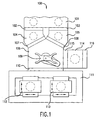
- FIG. 1 is an illustration of a lithography system 100 according to the present invention.
- Lithography system 100 patterns wafers, indicated by dashed circles within the FIG., that are obtained from a track 101. Wafers obtained from track 101 have undergone various processes as required prior to lithography patterning. For example, resist-apply, pre-bake, and other processes known to those skilled in the relevant art(s) are conducted on wafers prior to lithography patterning. After lithography patterning, wafers are returned to the track for further processing steps, such as development, post bake, and the like. Track 101 is connected to lithography system 100 via two gate valves 102, 103.
- Gate valves 102, 103 are of the type known to those skilled in the relevant art(s) as being capable of maintaining different atmospheric pressures on either side of the gate valve. Gate valves 102, 103 separate track 101 from two alignment load-locks 104, 105.
- Alignment load-locks 104, 105 are separated from a wafer exchange chamber 106 by gate valves 107, 108.
- Gate valves 107, 108 are analogous to gate valves 102, 103 that connect alignment load-locks 104, 105 to the track 101.
- Each alignment load-lock 104, 105 is thus a chamber separated from track 101 and wafer exchange chamber 106 by respective gate valves.
- Alignment load-locks 104, 105 are further connected to vacuum and venting elements (not shown) that allow the alignment load-locks to be transitioned from atmospheric pressure to vacuum (pumped-down) and back to atmospheric pressure again (vented). In this way, wafer exchange chamber 106 can be held at a high vacuum while track 101 is held at atmospheric pressure.
- Alignment load-locks 104, 105 thus serve to move wafers in and out of the wafer exchange chamber while transitioning from atmospheric pressure to high vacuum.
- the present inventors have discovered that by including alignment and chucking features within alignment load-locks 104, 105, overall system throughput can be greatly enhanced. Alignment load-locks 104, 105 will be discussed in greater detail below in connection with FIGs. 2a and 2b.
- Wafer exchange chamber 106 includes a robot 109 having a dual end-effector.
- Robot 109 is vacuum compatible and is capable of handling two chucks at once by virtue of its dual end-effctor.
- other structures can be used to transport the chuck with aligned wafer from the alignment load-lock to the lithography patterning chamber as would apparent to those skilled in the relevant arts given this disclosure.
- a robot having a single end-effector, or dual, non-robotic, transport mechanisms could also be used without departing from the scope of the present invention.
- Wafer exchange chamber 106 is connected to lithography patterning chamber 111 by gate valve 110.
- Gate valve 110 is similar to the other gate valves described herein.
- Lithography patterning chamber 111 includes wafer stages 112, 113. Wafer stages 112, 113 are capable of movement in the directions indicated for fine alignment and exposure processes. Lithography patterning chamber 111 thus further includes projection optics or other elements necessary to perform the lithography patterning. While lithography patterning chamber 111 includes two wafer stages 112, 113 a lithography patterning chamber could also include one wafer stage.
- a dual wafer stage structure like that shown is described in more detail in co-pending, commonly owned U.S. patent application No. 09/449,630, titled “Dual-Stage Lithography Apparatus and Method," filed November 30, 1999, which is hereby incorporated by reference in its entirety.
- Lithography system 100 further includes a holding load-lock 114.
- Holding load-lock 114 is used to hold a spare chuck, or to exchange chucks within the lithography system while maintaining lithography patterning. This allows access to a chuck held in holding load-lock for cleaning, for example.
- Holding load-lock 114 also includes gate valves 115 and 116. While the presence of holding load-lock is preferable, as it allows chuck exchange without stopping lithography patterning, it can be omitted without departing from the scope of the present invention.
- alignment load-locks 104, 105, and holding load-lock 114 are all preferably bi-directional load-locks, uni-directional load-locks could also be used without departing from the scope of the present invention.
- Unidirectional load-locks are capable of wafer input or wafer output only.
- Bidirectional load-locks are capable of both wafer input and wafer output.
- the wafer is transferred from track 101 to a unidirectional alignment load-lock and then to patterning chamber 111, it cannot then be transferred to the same unidirectional alignment load-lock after it has been patterned. Rather, after the patterning process is completed in the lithography patterning chamber, the wafer must instead be returned to another alignment load-lock and then, in turn, to track 101.
- the wafer can be transferred back through the same bidirectional alignment load-lock to track 101.
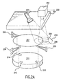
- FIGs. 2A and 2B together constitute an exploded view of the elements within an alignment load-lock according to the present invention.
- FIG. 2A corresponds to the upper portion of an alignment load-lock according to the present invention
- FIG. 2B corresponds to the lower portion of an alignment load-lock according to the present invention.
- the walls of the alignment load-lock are not shown in either of FIGs. 2A or 2B.
- Alignment load-lock roof 201 is an airtight transparent or semi-transparent window.
- a camera 202 and an illumination source 203 are disposed above alignment load-lock roof 201.
- alignment load-lock roof 201 is at least transparent to an inspection wavelength of light emitted from illumination source 203 to which camera 202 is sensitive.
- wafer supports 204, 205, 206 are used to hold a wafer 207. Wafer supports 204-206 are illustrated in the FIG. as hooks, but could also comprise pins, or other supporting mechanisms, as would be apparent to one skilled in the relevant art(s).
- Wafer 207 has been placed on wafer supports 204-206 from track 101 by an additional robot, which is customarily part of the track system (not shown). Moreover, wafer 207 can undergo prior coarse alignment so that notch 208 or other desired feature is placed within a field of view 209 of the camera 202, which is within an illumination field 210 of the illumination source 203. Such prior coarse alignment can be accomplished in a manner known to those skilled in the relevant art(s). For example, it can be performed by a module in the track that spins the wafer and locates the notch using a photoelectric sensor. Also included within the alignment load-lock shown is a chuck 211 having chuck cutouts 212, 213, and 214.
- Chuck cutouts 212-214 are large enough to accommodate a range of motion if the chuck such that wafer supports 204-206 can be accommodated within these chuck cutouts 212-214. Thus, chuck cutouts 212-214 line up approximately with wafer supports 204-206.
- FIG. 2B corresponds to the bottom portion of the alignment load-lock.
- alignment load-lock floor 216 having a motion feedthrough seal 217 is located at a bottom portion of the alignment load-lock.
- Motion feedthrough seal 217 allows movement of a column 230, upon which is disposed an alignment stage 218, with respect to the load-lock floor while preventing gas from flowing into the load lock.
- motion feedthrough seal 217 comprises bellows that will be described below in greater detail with respect to FIG. 3.
- other types of motion feedthrough seals such as a movable seal or a ferrofluidic seal, could be used without departing from the scope of the present invention.
- Alignment stage 218 include stage engagement mechanisms 219,220, and 221. Stage engagement mechanisms are used for kinematically mounting the chuck 211 with chuck engagement mechanisms 222-224 disposed on the lower surface of the chuck 211. In critical areas, the chuck engagement mechanisms can be kinematic hemispheres in order to avoid stress and strain, including, for example, hemispheres for engagement with vee-blocks 219-221 located on the various stages within the lithography system. In the embodiment shown, stage engagement mechanisms 219-221 comprise vee-blocks 219-221 that constitute the bottom half of a kinematic mount. Likewise, in the embodiment shown, chuck engagement mechanisms 222-224 comprise hemispheres that constitute the top half of the kinematic mount. As would be apparent to one skilled in the relevant art(s) given this description, other types of kinematic mounts can be used without departing from the scope of the present invention.
- chuck 211 is an electrostatic chuck capable of maintaining an electric charge sufficient to hold a wafer for an extended period of time. In one embodiment, however, chuck 211 is a vacuum chuck.
- Alignment stage 218 further includes contact block 225, having pogo contacts 226 and 227. Pogo contacts 226, 227 are used to make electrical contact with contact pads 228 and 229 disposed on the bottom of chuck 211.
- pogo contacts 226 and 227 are spring-loaded contacts made of metal tubing.
- the metal tubing comprises a spring with a metal bar. The metal bar contacts the contact pads 228 and 229.
- Chuck 211 is charged and discharged through contact pads 228 and 229 when connected to pogo contacts 226 and 227.
- electrostatic chucks While the present invention is described in terms of an electrostatic chuck, other chucks can be used without departing from the scope of the present invention.
- vacuum chucks, mechanical clamping, and other means of securing a wafer to a chuck could be used, as would be apparent to one skilled in the relevant art(s).
- electrostatic chucks Due to the high vacuum environment in which extreme ultraviolet light processing occurs, electrostatic chucks are preferable.
- Alignment stage 218 is positioned at the top of column 230.
- Column 230 is disposed atop an alignment substage 231, which is held by an alignment substage mount 232.
- Additional motor and control elements (not shown) are used to move the alignment stage in four degrees of freedom (rotation, two horizontal translations, and a vertical translation) and as indicated by the arrows in the FIG., as would be apparent to a person skilled in the relevant art(s), given this description.
- Motion feedthrough seal 217 serves to separate the high vacuum environment within the alignment load-lock from the alignment substage 231, alignment substage mount 232, and the remainder of the lithography system.
- chuck 211 and wafer 207 are not integral parts of the alignment load-lock. Rather, chuck 211 is one of a number of like chucks which are used within the lithography system 100. Likewise, wafer 207 has been obtained from track 101 for lithography patterning within lithography patterning chamber 111, of the system shown in FIG. 1. As mentioned above, wafer 207 may have undergone coarse alignment prior to being placed on wafer supports 204-206. This coarse alignment can be performed in order to place notch 208 within the field of view 209 of camera 202.
- the camera 202 can determine both the center of the wafer from the radius of curvature visible within the field of view 209 as well as the orientation of the wafer from the location of notch 208.
- a plurality of such cameras and light sources 203 can be used without departing from the scope of the present invention. Since camera 202 is used for determining notch location 208 as well as the radius of curvature of wafer 206, the use of more than one camera can increase the precision of the observations, as would be apparent to one skilled in the relevant art(s) given this disclosure. Best results would be obtained with two diametrically opposed cameras (or equally spaced cameras, in reference to the wafer).
- Camera 202 looks at field of view 209 to determine wafer location 207. This wafer location is then output by camera 202 to a pattern recognition unit 233 (not shown).
- the pattern recognition unit sends location information to alignment substage 231. Since the pattern recognition unit knows the precise orientation and location of wafer 207 it can control the location of alignment stage 218 through alignment substage 231 and alignment substage mount 232.
- chuck 211 is moved up to and put in contact with wafer 207.
- chuck 211 is charged through contact pads 228 and 229, which are in contact with pogo contacts 226 and 227 at contact block 225 of alignment stage 218.
- chuck 211 Since chuck 211 has been aligned with wafer 207 prior to chuck 211 being charged, wafer 207 is firmly held in contact with chuck 211 by virtue of the charge. Since each wafer stage 112, 113 within lithography patterning chamber 111 includes kinematic mounts, the repeatability of chuck placement on wafer stages 112, 113 within the lithography patterning chamber is limited to the accuracy of the kinematic mounts.
- the kinematic mounts shown which use vee-blocks and hemispheres, have a repeatability of about two microns. Since chuck 211 can maintain its electrostatic charge within the lithography system 100, the alignment of a wafer, for example, wafer 207, will always be within the repeatability of the kinematic mounts used.
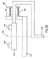
- FIG. 3A is an illustration of a floor-mounted motion feedthrough 300 within a lithography system of the present invention.
- Bellows 302 allow vertical and horizontal translations of shaft 230 relative to load-lock floor 216, while maintaining vacuum inside the load lock.
- Bellows 302 include a plurality of metal, preferably stainless steel disks welded at their peripheral and inside edges. These bellows allow column 230 to move in six degrees of freedom while maintaining a vacuum seal.
- Rotary seal 304 allows rotation of shaft 230, while maintaining a vacuum.
- Bearing 306 captures shaft flange 308, preventing collapse of the bellows due to atmospheric pressure.
- seal 304 can be an elastomer seal, a pre-loaded teflon seal, or a ferrofluidic seal. It will also be apparent that the transfer of rotary motion accomplished by 304-308 could have also been accomplished via a magnetic coupling.
- FIG. 3B is an illustration of a wall-mounted motion feedthrough 350 within a lithography system of the present invention.
- Bellows 352, attached to chamber wall 354, allows vertical and horizaontal translation of alignment stage 218.
- Bellows 352 also allow a limited amount of rotation of alignment stage 218 about its centerline 356. This arrangement does not require a rotary seal, and is, therefore, less leak-prone than the apparatus of FIG. 3A.
- the rotary seal 304 of FIG. 3A allows unlimited rotation
- the bellows 352 only allow a few degrees of rotational freedom. The limited amount of rotation is sufficient if a coarse alignment step is performed on the wafer (by the track) before introducing the wafer in the load-lock.
- a second wall-mounted feedthrough mechanism could be added diametrically opposite to the one shown through a hole in an opposite wall in order to improve mechanical stability of the apparatus, without deviating from the present invention.
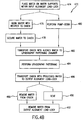
- FIG. 4A is an illustration of a method 400 of patterning a wafer within a lithography system utilizing at least one bidirectional alignment load-lock according to the present invention.
- a system can comprise only one bidirectional alignment load-lock or a plurality of bidirectional alignment load-locks to increase efficiency and throughput.
- the bidirectional alignment load-lock(s) is capable of accepting the wafer from track 101 as it enters the lithography system (input) and also allowing the wafer to enter it after patterning and be dispelled from it back to track 101 (output).
- the wafer can be transferred from track 101 to the bidirectional alignment load-lock, from the bidirectional alignment load-lock to the patterning chamber, from the patterning chamber after patterning to the same bidirectional alignment load-lock, and then from the bidirectional alignment load-lock to the track 101.
- a wafer is placed on wafer supports within a bidirectional alignment load-lock(s).
- the wafer can be taken from a track before being placed onto supports within the bidirectional alignment load-lock(s). Placing the wafer on the supports within the bidirectional alignment load-lock(s) can be accomplished with, for example, a robot.
- the wafer supports within the bidirectional alignment load-lock(s) can comprise hooks, pins, and the like.
- the bidirectional alignment load-lock(s) can comprise a conventional load-lock chamber with gate valves separating a track from a wafer transport chamber.
- a wafer transport chamber In a lithography system operating at high vacuum, such a wafer transport chamber would be kept at high vacuum while the track would be kept at atmospheric pressure.
- the bidirectional alignment load-lock(s) is thus used to transfer wafers in and out of the high vacuum environment within the lithography apparatus itself without exposing the entire apparatus to atmospheric pressure.
- the wafer is aligned with respect to a chuck.
- the chuck can be an electrostatic chuck, a vacuum chuck, or a chuck with other mechanical clamping features.
- the aligned wafer is secured to the chuck.
- the securing of the aligned wafer to the chuck 421 can be accomplished by moving the chuck up to and in contact with the wafer and then, in the case of an electrostatic chuck, charging the electrostatic chuck to thereby secure the wafer to the chuck.
- Such charging can be accomplished through the use of pogo contacts on an alignment stage which are in contact with pads on the bottom surface of the electrostatic chuck. Further details of steps 420 and 421 are described in greater detail below in connection with FIG. 5.
- a pump-down is performed within the bidirectional alignment load-lock(s).
- pump-down is the procedure whereby the load-lock is evacuated of gases thus bringing it from atmospheric pressure to high vacuum.
- the present inventors have discovered that by performing the pump-down operation simultaneously with the alignment of the wafer with respect to the chuck and the securing of the wafer to the chuck, greater throughput can be realized within a lithography system according to the present invention.
- a next step 430 the chuck with the aligned wafer is transported to a lithography patterning chamber.
- the transportation of the chuck from the bidirectional alignment load-lock(s) to the lithography patterning chamber can be accomplished by a robot located within a wafer exchange chamber disposed between the bidirectional alignment load-lock(s) and the lithography patterning chamber.
- a robot can have a dual end defector to realize greater efficiency of transportation of chucks between bidirectional alignment load-lock(s) and the lithography patterning chamber.
- the chuck and wafer could be placed on a kineumatic mount of the exposure stage.
- lithography patterning is performed in a next step 440.
- Such lithography patterning can include a final alignment step as well as additional steps used within lithography patterning as are known to those skilled in the relevant art(s).
- a next step 450 the chuck with processed wafer are removed from the kineumatic mount of the exposure stage to a bidirectional alignment load-lock(s) from the lithography patterning chamber.
- the transportation of the chuck with the processed wafer from the lithography patterning chamber to the bidirectional alignment load-lock(s) can be performed with a robot located within a wafer exchange chamber.
- the chuck with patterned wafer can be brought back to the same bidirectional alignment load-lock(s) through which it entered the system.
- a next step 460 the processed wafer is removed from the chuck within the bidirectional alignment load-lock(s).
- This step is substantially the reverse of process step 421, discussed above.
- the chuck can be discharged. Once discharged, the chuck can be lowered away from the wafer leaving the wafer held by the wafer supports.
- a venting operation is performed at a concurrent step 465. Venting is the process by which the pressure within the bidirectional alignment load-lock(s) is brought from high vacuum back to atmospheric pressure.
- the venting step 465 is performed simultaneously with step 460.
- performing venting while removing the wafer from the chuck further increases the throughput of a lithography system according to the present invention.
- a final step 470 the now patterned wafer is removed from the bidirectional alignment load-lock(s) and placed back onto the track.
- the wafer can be placed onto another structure used to move wafers away from the lithography apparatus.
- the lithography system has been returned to its condition existing prior to the first step, 410. Accordingly, method 400 can be repeated indefinitely for the lithography patterning of multiple wafers.
- FIG. 4B is an illustration of a method 472 of patterning a wafer within a lithography system utilizing unidirectional alignment load-lock(s) according to the present invention.
- a wafer is placed on wafer supports within an input alignment load-lock.
- the input alignment load-lock is unidirectional, as the wafer does not exit the system through the same alignment load-lock through which it entered the system. Rather, it is returned to another alignment load-lock (output alignment load-lock) after it undergoes patterning in the patterning chamber and exits the system (i.e., transferred to track 101) through the output alignment load-lock.
- the wafer can be taken from a track before being placed onto supports within the input alignment load-lock. Placing the wafer on the supports within the input alignment load-lock can be accomplished with, for example, a robot.
- the wafer supports within the input alignment load-lock can comprise hooks, pins, and the like.
- the input alignment load-lock can comprise a conventional input load-lock chamber with gate valves separating a track from a wafer transport chamber. In a lithography system operating at high vacuum, such a wafer transport chamber would be kept at high vacuum while the track would be kept at atmospheric pressure. The input alignment load-lock is thus used to transfer wafers into the high vacuum environment within the lithography apparatus itself without exposing the entire apparatus to atmospheric pressure.
- a next step 476 the wafer is aligned with respect to a chuck.
- the chuck can be an electrostatic chuck, a vacuum chuck, or a chuck with other mechanical clamping features.
- the aligned wafer is secured to the chuck.
- the securing of the aligned wafer to the chuck can be accomplished by moving the chuck up to and in contact with the wafer and then, in the case of an electrostatic chuck, charging the electrostatic chuck to thereby secure the wafer to the chuck.
- Such charging can be accomplished through the use of pogo contacts on an alignment stage which are in contact with pads on the bottom surface of the electrostatic chuck. Further details of steps 476 and 478 are described in greater detail below in connection with FIG. 5.
- a pump-down is performed within the input alignment load-lock.
- the chuck with the aligned wafer is transported to a lithography patterning chamber.
- the transportation of the chuck from the input alignment load-lock to the lithography patterning chamber can be accomplished by a robot located within a wafer exchange chamber disposed between the input alignment load-lock and the lithography patterning chamber.
- other structures can be used to transport the chuck with aligned wafer from the input alignment load-lock to the lithography patterning chamber, as would apparent to those skilled in the relevant art(s) given this disclosure.
- the chuck and wafer could be placed on a kineumatic mount of the exposure stage.
- lithography patterning is performed in a next step 484.
- Such lithography patterning can include a final alignment step as well as additional steps used within lithography patterning as are known to those skilled in the relevant art(s).
- a next step 486 the chuck with processed wafer are removed from the kineumatic mount of the exposure stage to an output alignment load-lock from the lithography patterning chamber.
- the output alignment load-lock is not the same alignment load-lock as the input alignment load-lock.
- the wafer is only transferred through the output alignment load-lock after it has exited the lithography patterning chamber and needs to be transferred back to track 101.
- the transportation of the chuck with the processed wafer from the lithography patterning chamber to the output alignment load-lock can be performed with a robot located within a wafer exchange chamber.
- a next step 488 the processed wafer is removed from the chuck within the output alignment load-lock.
- This step is substantially the reverse of process step 478, discussed above.
- the chuck can be discharged. Once discharged, the chuck can be lowered away from the wafer leaving the wafer held by the wafer supports.
- a venting operation is performed at a concurrent step 490. As with steps 476, 478, and 480, the venting step 480 is performed simultaneously with step 476.
- a final step 492 the now processed wafer is removed from the output alignment load-lock and placed back onto the track.
- the wafer can be placed onto another structure used to move wafers away from the lithography apparatus.
- the lithography system has been returned to its condition existing prior to the first step, 474. Accordingly, method 472 can be repeated indefinitely for the lithography patterning of multiple wafers.
- FIG. 5 is an illustration of a method 500 of aligning a wafer within an alignment load-lock according to the present invention.
- a wafer is placed on wafer supports.
- wafer supports can include hooks, pins, and the like.
- the wafer can be placed on the wafer supports through the use of a robot or other wafer transport mechanisms, as would be apparent to one skilled in the relevant art(s).
- a next step 520 the wafer's orientation and location is observed.
- Such observation can be conducted, for example, with a camera and illumination source located outside of the alignment load-lock, as described above in connection with FIG. 2A.
- the wafer's location is observed by the camera by analyzing the wafer's radius of curvature observed within the camera's field of view.
- location as used herein in connection with a wafer means the location of the wafer within an XY plane.
- a pattern recognition unit Such pattern recognition units and their operation in connection with a camera and illumination source like the type described herein are well known to those skilled in the relevant art(s).
- the wafer's particular orientation (i.e. its angular orientation about its center) is determined by noting the location of a notch within the wafer that is also located within the camera's field of view.
- coarse alignment can take place prior to the method shown in FIG. 5.
- Such coarse alignment can include, for example, the use of a wafer spinning module with an edge sensor which can be located inside the track.
- Such a coarse pre-alignment technique is known to those skilled in the relevant art(s) and so will not be discussed more fully herein. While the observation of wafer location and orientation has been described in terms of a single camera, multiple cameras with narrow fields of view can be used to enhance the accuracy of the alignment. By using multiple cameras directed at different viewpoints along the circumference of the wafer, the location of the center and the orientation of the notch can be more precisely determined than by using a single camera.
- a chuck is moved so as to align the wafer relative to the chuck.
- a chuck can be an electrostatic chuck, a vacuum chuck, and the like.
- the chuck is moved relative to the wafer through the use of an alignment stage like that described in connection with FIG. 2B. Movements of the alignment stage are controlled by the same pattern recognition unit that receives data from the camera used to observe the wafer.
- the pattern recognition unit knows the precise location of the wafer.
- the pattern recognition unit also knows the precise location of the alignment stage by virtue of location feedback from the alignment stage.
- the pattern recognition unit can cause the alignment stage to move the chuck relative to the wafer until the wafer is aligned relative to the chuck (the diameter of the chuck is purposely a little larger than the diameter of the wafer).
- a subsequent step 530 of placing the chuck in contact with the wafer is performed. This can be accomplished, for example, by moving the chuck upwards until it is in physical contact with the wafer's bottom surface.
- the chuck can have, for example, cutouts to accommodate the wafer supports holding the wafer. Thus, when the chuck is moved upwards into contact with the wafer's bottom surface, the wafer supports will not interfere with the chuck because they are located within the chuck cutouts.
- the chuck is secured to the wafer in a next step 540.
- Securing the chuck to the wafer can be accomplished by charging the chuck, in the case of an electrostatic chuck.
- securing the chuck to the wafer can be performed by activating a vacuum within a vacuum chuck.
- Other methods of securing the chuck to the wafer can be performed without departing from the scope of the present invention.
- the chuck can be moved around within a lithography system according to the present invention all the while maintaining alignment with the wafer. Since the chuck is equipped with kinematic mounting features, the alignment of the wafer relative to the exposure stage will always be within the repeatability of the kinematic mounts used within the lithography system. Typically, the repeatability of such kinematic mounts is within approximately two microns. On the other hand, the repeatability of a robot and gripper is typically a few hundred microns. Therefore, the conventional steps of performing fine alignment subsequent to robot movements can be avoided by moving wafers while attached to chucks. Fine alignment will still be needed.
- a lithography system according to the present invention can achieve high levels of throughput, for example 120 wafers per hour, by using multiple chucks within the system.
- an alignment load-lock could be an alignment and chucking station without the pump-down and venting characteristics of a load-lock.
- a method could be performed according to the present invention without the described pump-down and venting steps.
Abstract
Description
- The present invention relates to a wafer handling system and method for use within a lithography system. More particularly, this invention relates to a system and method of wafer handling in which wafers are transported within a lithography system while being affixed and aligned to chucks, thereby maximizing production throughput.
- Lithography is a process used to create features on the surface of substrates. Such substrates can include those used in the manufacture of flat panel displays, circuit boards, various integrated circuits, and the like. A frequently used substrate for such applications is a semiconductor wafer. While this description is written in terms of a semiconductor wafer for illustrative purposes, one skilled in the art would recognize that this description also applies to other types of substrates known to those skilled in the art. During lithography, a wafer, which is disposed on a wafer stage, is exposed to an image projected onto the surface of the wafer by exposure optics located within a lithography apparatus. While exposure optics are used in the case of photolithography, a different type of exposure apparatus may be used depending on the particular application. For example, x-ray, ion, electron, or photon lithographies each may require a different exposure apparatus, as is known to those skilled in the art. The particular example of photolithography is discussed here for illustrative purposes only.
- The projected image produces changes in the characteristics of a layer, for example photoresist, deposited on the surface of the wafer. These changes correspond to the features projected onto the wafer during exposure. Subsequent to exposure, the layer can be etched to produce a patterned layer. The pattern corresponds to those features projected onto the wafer during exposure. This patterned layer is then used to remove exposed portions of underlying structural layers within the wafer, such as conductive, semiconductive, or insulative layers. This process is then repeated, together with other steps, until the desired features have been formed on the surface of the wafer.
- Step-and-scan technology works in conjunction with a projection optics system that has a narrow imaging slot. Rather than expose the entire wafer at one time, individual fields are scanned onto the wafer one at a time. This is done by moving the wafer and reticle simultaneously such that the imaging slot is moved across the field during the scan. The wafer stage must then be stepped between field exposures to allow multiple copies of the reticle pattern to be exposed over the wafer surface. In this manner, the sharpness of the image projected onto the wafer is maximized. Through increases in both alignment precision and projection accuracy, today's lithography tools are capable of producing devices with ever decreasing minimum feature size. However, minimum feature size is but one measure of a lithography tool's utility. Another critical measure is throughput.
- Throughput refers to the number of wafers per hour that can be patterned by a lithography system. Every task that must be performed on wafers within a lithography system contributes to the total time required to pattern the wafers, with an associated decrease in throughput. One critical task that must be performed repeatedly within a lithography system is wafer alignment. Wafers must be precisely aligned within a lithography system in order to achieve high levels of overlay accuracy. Unfortunately, alignment precision is usually lost whenever wafers are moved within conventional lithography systems with robots.
- What is needed is a system and method for handling wafers within a lithography system that both avoids the loss of alignment caused by conventional robots, while at the same time improving system throughput.
- In one embodiment, the present invention includes a lithography system having a lithography patterning chamber, a wafer exchange chamber separated from the lithography patterning chamber by a first gate valve, and at least one alignment load-lock separated from the wafer exchange chamber by a second gate valve. The alignment load-lock includes an alignment stage that aligns a wafer during pump-down. An alignment load-lock according to the present invention can be uni-directional or bi-directional. Likewise, a lithography system according to the present invention can include one or multiple alignment load-locks.
- A lithography system according to the present invention can also include a holding load-lock separated from the wafer exchange chamber.
- A lithography system according to the present invention can further include an illumination source that emits light having an inspection wavelength, and a camera sensitive to said inspection wavelength. A roof of the alignment load-lock is transparent to the inspection wavelength to allow observation of the wafer contained within the alignment load-lock.
- Also included within the alignment load lock according to an embodiment of the present invention are supports for holding a wafer. These supports can be hooks, pins, and the like. An alignment stage is further located within the alignment load lock. The alignment stage is separated from an alignment sub-stage disposed outside of the alignment load-lock by a column extending through a floor of the alignment load-lock. Furthermore, the floor of the alignment load-lock can include a motion feedthrough seal that allows the column to move relative to the floor while preventing gas flow into the alignment load-lock. Such a motion feedthrough seal can include bellows and rotary seals such as ferromagnetic seals.
- Further included in an embodiment of the present invention are multiple chucks. The chucks can be electrostatic chucks or vacuum chucks. The chucks can include cutouts for accommodating the wafer supports within the alignment load-lock. The chucks can further include chuck engagement mechanisms for kinematically mounting the chucks to the alignment stage or to a stage located within the lithography patterninging chamber. In critical areas, the chuck engagement mechanisms can be kinematic hemispheres in order to avoid stress and strain, including, for example, hemispheres for engagement with vee-blocks located on the various stages within the lithography system.
- In an embodiment of the present invention, the lithography patterninging chamber can include multiple exposure stages.
- Also disclosed is a method of patterning a wafer within a lithography system. In an embodiment, the method includes a first step of placing the wafer on supports within an alignment load-lock. In a next step, the wafer is aligned with respect to a chuck while the wafer is supported within the alignment load-lock on the supports. In another step, the wafer is secured to the chuck. And in yet another step, pump-down is performed to create a vacuum within the alignment load-lock.
- In a method according to the present invention, pump-down can be performed concurrently with aligning the wafer relative to the chuck. Likewise, pump-down can be performed concurrently with securing the wafer to the chuck subsequent to the alignment step.
- A method according to an embodiment of the present invention can also include a step of transporting the chuck and wafer to a lithography patterning chamber. Further fine alignment may be needed in the lithography patterning chamber. Next, a step of performing lithography patterning on the wafer is conducted. Once the lithography patterning is complete, the wafer and chuck are returned to the alignment load-lock area. Once back at the alignment load-lock, the chuck can be removed from the wafer and venting can be performed. The venting can take place while the wafer is being removed from the chuck.
- Also disclosed herein is a method of aligning a wafer within an alignment load-lock. In an embodiment, this method includes a first step of placing the wafer on supports within the alignment load-lock. Next, a step of observing the location and orientation of the wafer on the supports within the alignment load-lock is performed. Also performed is a step of moving a chuck so as to align the wafer with respect to the chuck. Once aligned, the chuck is then placed in contact with, and secured to, the wafer. The step of observing the location and orientation of the wafer can be performed by a camera located outside of the alignment load-lock.
- The accompanying drawings, which are incorporated herein and form part of the specification, are illustrations of the present invention and, together with the description, further serve to explain the principles of the invention and to enable a person skilled in the pertinent art to make and use the invention. Like reference numbers refer to like elements within the different FIG.s.
- FIG. 1 is an illustration of a lithography system according to the present invention.
- FIG. 2A is an exploded view of the upper elements within an alignment load-lock according to the present invention.
- FIG. 2B is an exploded view of the lower elements within an alignment load-lock according to the present invention.
- FIG. 3A is an illustration of a floor-mounted
motion feedthrough 300 within a lithography system according to the present invention. - FIG. 3B is an illustration of a wall-mounted
motion feedthrough 350 within a lithography system according to the present invention. - FIG. 4A is an illustration of a method of patterning a wafer within a lithography system utilizing a bidirectional load-lock(s) according to the present invention.
- FIG. 4B is an illustration of a method of patterning a wafer within a lithography system utilizing a unidirectional load-lock(s) according to the present invention.
- FIG. 5 is an illustration of a method of aligning a wafer within an alignment load-lock according to the present invention.
- As used herein, the term wafer means a semiconductor wafer, or any other substrate suitable for lithographic patterning.
- Alignment, pump-down, and charging of an electrostatic chuck are all procedures that take up precious time within a lithography patterning process. The present inventors have discovered that all three of these functions can be combined into a single alignment load-lock station. Such a single alignment load-lock station can align a wafer with respect to a chuck and then secure that wafer to the chuck, all the while pumping-down the load-lock. By including more than one chuck within such a lithography system, wafers can be secured to their respective chucks during lithography patterning, thereby maximizing throughput.
- FIG. 1 is an illustration of a
lithography system 100 according to the present invention.Lithography system 100 patterns wafers, indicated by dashed circles within the FIG., that are obtained from atrack 101. Wafers obtained fromtrack 101 have undergone various processes as required prior to lithography patterning. For example, resist-apply, pre-bake, and other processes known to those skilled in the relevant art(s) are conducted on wafers prior to lithography patterning. After lithography patterning, wafers are returned to the track for further processing steps, such as development, post bake, and the like.Track 101 is connected tolithography system 100 via twogate valves Gate valves Gate valves separate track 101 from two alignment load-locks - Alignment load-
locks wafer exchange chamber 106 bygate valves Gate valves gate valves locks track 101. Each alignment load-lock track 101 andwafer exchange chamber 106 by respective gate valves. Alignment load-locks wafer exchange chamber 106 can be held at a high vacuum whiletrack 101 is held at atmospheric pressure. Alignment load-locks locks locks -
Wafer exchange chamber 106 includes arobot 109 having a dual end-effector.Robot 109 is vacuum compatible and is capable of handling two chucks at once by virtue of its dual end-effctor. Alternatively, other structures can be used to transport the chuck with aligned wafer from the alignment load-lock to the lithography patterning chamber as would apparent to those skilled in the relevant arts given this disclosure. For example, a robot having a single end-effector, or dual, non-robotic, transport mechanisms could also be used without departing from the scope of the present invention. -
Wafer exchange chamber 106 is connected tolithography patterning chamber 111 bygate valve 110.Gate valve 110 is similar to the other gate valves described herein.Lithography patterning chamber 111 includes wafer stages 112, 113. Wafer stages 112, 113 are capable of movement in the directions indicated for fine alignment and exposure processes.Lithography patterning chamber 111 thus further includes projection optics or other elements necessary to perform the lithography patterning. Whilelithography patterning chamber 111 includes twowafer stages 112, 113 a lithography patterning chamber could also include one wafer stage. A dual wafer stage structure like that shown is described in more detail in co-pending, commonly owned U.S. patent application No. 09/449,630, titled "Dual-Stage Lithography Apparatus and Method," filed November 30, 1999, which is hereby incorporated by reference in its entirety. -
Lithography system 100 further includes a holding load-lock 114. Holding load-lock 114 is used to hold a spare chuck, or to exchange chucks within the lithography system while maintaining lithography patterning. This allows access to a chuck held in holding load-lock for cleaning, for example. Holding load-lock 114 also includesgate valves - While alignment load-
locks lock 114 are all preferably bi-directional load-locks, uni-directional load-locks could also be used without departing from the scope of the present invention. Unidirectional load-locks are capable of wafer input or wafer output only. Bidirectional load-locks, however, are capable of both wafer input and wafer output. - For example, if the wafer is transferred from
track 101 to a unidirectional alignment load-lock and then to patterningchamber 111, it cannot then be transferred to the same unidirectional alignment load-lock after it has been patterned. Rather, after the patterning process is completed in the lithography patterning chamber, the wafer must instead be returned to another alignment load-lock and then, in turn, to track 101. - By contrast, if the wafer is transferred from
track 101 to a bidirectional alignment load-lock and then tolithography patterning chamber 111, after patterning, the wafer can be transferred back through the same bidirectional alignment load-lock to track 101. - While the use of two bi-directional alignment load-locks is advantageous as it allows for greater system throughput, two single unidirectional load-locks could also be used. Likewise, a single bi-directional alignment load-lock could also be used without departing from the scope of the present invention. The precise structure and function of each of alignment load-
locks - FIGs. 2A and 2B together constitute an exploded view of the elements within an alignment load-lock according to the present invention. FIG. 2A corresponds to the upper portion of an alignment load-lock according to the present invention, while FIG. 2B corresponds to the lower portion of an alignment load-lock according to the present invention. The walls of the alignment load-lock are not shown in either of FIGs. 2A or 2B.
- Alignment load-
lock roof 201 is an airtight transparent or semi-transparent window. Acamera 202 and anillumination source 203 are disposed above alignment load-lock roof 201. By "semi-transparent," it is meant that alignment load-lock roof 201 is at least transparent to an inspection wavelength of light emitted fromillumination source 203 to whichcamera 202 is sensitive. Within the alignment load-lock are wafer supports 204, 205, 206. These wafer supports 204-206 are used to hold awafer 207. Wafer supports 204-206 are illustrated in the FIG. as hooks, but could also comprise pins, or other supporting mechanisms, as would be apparent to one skilled in the relevant art(s).Wafer 207 has been placed on wafer supports 204-206 fromtrack 101 by an additional robot, which is customarily part of the track system (not shown). Moreover,wafer 207 can undergo prior coarse alignment so thatnotch 208 or other desired feature is placed within a field ofview 209 of thecamera 202, which is within anillumination field 210 of theillumination source 203. Such prior coarse alignment can be accomplished in a manner known to those skilled in the relevant art(s). For example, it can be performed by a module in the track that spins the wafer and locates the notch using a photoelectric sensor. Also included within the alignment load-lock shown is achuck 211 havingchuck cutouts - FIG. 2B corresponds to the bottom portion of the alignment load-lock. Specifically, alignment load-
lock floor 216 having amotion feedthrough seal 217 is located at a bottom portion of the alignment load-lock.Motion feedthrough seal 217 allows movement of acolumn 230, upon which is disposed analignment stage 218, with respect to the load-lock floor while preventing gas from flowing into the load lock. In the particular embodiment shown,motion feedthrough seal 217 comprises bellows that will be described below in greater detail with respect to FIG. 3. Alternatively, other types of motion feedthrough seals, such as a movable seal or a ferrofluidic seal, could be used without departing from the scope of the present invention. -
Alignment stage 218 include stage engagement mechanisms 219,220, and 221. Stage engagement mechanisms are used for kinematically mounting thechuck 211 with chuck engagement mechanisms 222-224 disposed on the lower surface of thechuck 211. In critical areas, the chuck engagement mechanisms can be kinematic hemispheres in order to avoid stress and strain, including, for example, hemispheres for engagement with vee-blocks 219-221 located on the various stages within the lithography system. In the embodiment shown, stage engagement mechanisms 219-221 comprise vee-blocks 219-221 that constitute the bottom half of a kinematic mount. Likewise, in the embodiment shown, chuck engagement mechanisms 222-224 comprise hemispheres that constitute the top half of the kinematic mount. As would be apparent to one skilled in the relevant art(s) given this description, other types of kinematic mounts can be used without departing from the scope of the present invention. - In the embodiment shown,
chuck 211 is an electrostatic chuck capable of maintaining an electric charge sufficient to hold a wafer for an extended period of time. In one embodiment, however, chuck 211 is a vacuum chuck.Alignment stage 218 further includescontact block 225, havingpogo contacts contacts contact pads chuck 211. In one embodiment,pogo contacts contact pads Chuck 211 is charged and discharged throughcontact pads contacts -
Alignment stage 218 is positioned at the top ofcolumn 230.Column 230 is disposed atop analignment substage 231, which is held by analignment substage mount 232. Additional motor and control elements (not shown) are used to move the alignment stage in four degrees of freedom (rotation, two horizontal translations, and a vertical translation) and as indicated by the arrows in the FIG., as would be apparent to a person skilled in the relevant art(s), given this description.Motion feedthrough seal 217 serves to separate the high vacuum environment within the alignment load-lock from thealignment substage 231,alignment substage mount 232, and the remainder of the lithography system. - Operation of the elements within the alignment load-lock will now be described. It should be noted that
chuck 211 andwafer 207 are not integral parts of the alignment load-lock. Rather, chuck 211 is one of a number of like chucks which are used within thelithography system 100. Likewise,wafer 207 has been obtained fromtrack 101 for lithography patterning withinlithography patterning chamber 111, of the system shown in FIG. 1. As mentioned above,wafer 207 may have undergone coarse alignment prior to being placed on wafer supports 204-206. This coarse alignment can be performed in order to placenotch 208 within the field ofview 209 ofcamera 202. Sincecamera 202 can see notch 208, thecamera 202 can determine both the center of the wafer from the radius of curvature visible within the field ofview 209 as well as the orientation of the wafer from the location ofnotch 208. In this respect, it should be noted that while onecamera 202 has been shown in FIG. 2A, a plurality of such cameras andlight sources 203 can be used without departing from the scope of the present invention. Sincecamera 202 is used for determiningnotch location 208 as well as the radius of curvature ofwafer 206, the use of more than one camera can increase the precision of the observations, as would be apparent to one skilled in the relevant art(s) given this disclosure. Best results would be obtained with two diametrically opposed cameras (or equally spaced cameras, in reference to the wafer). -
Camera 202 looks at field ofview 209 to determinewafer location 207. This wafer location is then output bycamera 202 to a pattern recognition unit 233 (not shown). The pattern recognition unit sends location information toalignment substage 231. Since the pattern recognition unit knows the precise orientation and location ofwafer 207 it can control the location ofalignment stage 218 throughalignment substage 231 andalignment substage mount 232. Oncechuck 211 has been aligned withwafer 207,chuck 211 is moved up to and put in contact withwafer 207. Once in contact withwafer 207,chuck 211 is charged throughcontact pads pogo contacts contact block 225 ofalignment stage 218. Sincechuck 211 has been aligned withwafer 207 prior to chuck 211 being charged,wafer 207 is firmly held in contact withchuck 211 by virtue of the charge. Since eachwafer stage lithography patterning chamber 111 includes kinematic mounts, the repeatability of chuck placement onwafer stages chuck 211 can maintain its electrostatic charge within thelithography system 100, the alignment of a wafer, for example,wafer 207, will always be within the repeatability of the kinematic mounts used. - Returning to FIG. 1, it should be apparent from the above discussion in connection with FIGs. 2A and 2B that while a wafer is within either of alignment load-
locks lock 104 or alignment load-lock 105 has been aligned with respect to a chuck and attached to that chuck, and pumpdown is complete, thegate valve point robot 109 can lift the chuck and wafer together from within either alignment load-lock and move it to thelithography patterning chamber 111. Sincerobot 109 includes a gripper, it can hold two chucks at once. Thus,robot 109 can swiftly exchange chucks between either alignment load-lock station and either wafer stage. - FIG. 3A is an illustration of a floor-mounted
motion feedthrough 300 within a lithography system of the present invention.Bellows 302 allow vertical and horizontal translations ofshaft 230 relative to load-lock floor 216, while maintaining vacuum inside the load lock.Bellows 302 include a plurality of metal, preferably stainless steel disks welded at their peripheral and inside edges. These bellows allowcolumn 230 to move in six degrees of freedom while maintaining a vacuum seal.Rotary seal 304 allows rotation ofshaft 230, while maintaining a vacuum. Bearing 306 capturesshaft flange 308, preventing collapse of the bellows due to atmospheric pressure. It will be apparent to one skilled in the art that seal 304 can be an elastomer seal, a pre-loaded teflon seal, or a ferrofluidic seal. It will also be apparent that the transfer of rotary motion accomplished by 304-308 could have also been accomplished via a magnetic coupling. - FIG. 3B is an illustration of a wall-mounted
motion feedthrough 350 within a lithography system of the present invention.Bellows 352, attached tochamber wall 354, allows vertical and horizaontal translation ofalignment stage 218.Bellows 352 also allow a limited amount of rotation ofalignment stage 218 about itscenterline 356. This arrangement does not require a rotary seal, and is, therefore, less leak-prone than the apparatus of FIG. 3A. However, whereas therotary seal 304 of FIG. 3A allows unlimited rotation, thebellows 352 only allow a few degrees of rotational freedom. The limited amount of rotation is sufficient if a coarse alignment step is performed on the wafer (by the track) before introducing the wafer in the load-lock. It will be understood that a second wall-mounted feedthrough mechanism could be added diametrically opposite to the one shown through a hole in an opposite wall in order to improve mechanical stability of the apparatus, without deviating from the present invention. - FIG. 4A is an illustration of a
method 400 of patterning a wafer within a lithography system utilizing at least one bidirectional alignment load-lock according to the present invention. It should be noted that such a system can comprise only one bidirectional alignment load-lock or a plurality of bidirectional alignment load-locks to increase efficiency and throughput. In the embodiment utilizing a bidirectional alignment load-lock system, unlike the embodiment utilizing a unidirectional alignment load-lock system, the bidirectional alignment load-lock(s) is capable of accepting the wafer fromtrack 101 as it enters the lithography system (input) and also allowing the wafer to enter it after patterning and be dispelled from it back to track 101 (output). In other words, the wafer can be transferred fromtrack 101 to the bidirectional alignment load-lock, from the bidirectional alignment load-lock to the patterning chamber, from the patterning chamber after patterning to the same bidirectional alignment load-lock, and then from the bidirectional alignment load-lock to thetrack 101. - In a
first step 410 of themethod 400 of FIG. 4A, a wafer is placed on wafer supports within a bidirectional alignment load-lock(s). As described above in connection with FIG. 1, the wafer can be taken from a track before being placed onto supports within the bidirectional alignment load-lock(s). Placing the wafer on the supports within the bidirectional alignment load-lock(s) can be accomplished with, for example, a robot. As described above in connection with FIG. 2A, the wafer supports within the bidirectional alignment load-lock(s) can comprise hooks, pins, and the like. Also, as described above in connection with FIG. 1, the bidirectional alignment load-lock(s) can comprise a conventional load-lock chamber with gate valves separating a track from a wafer transport chamber. In a lithography system operating at high vacuum, such a wafer transport chamber would be kept at high vacuum while the track would be kept at atmospheric pressure. The bidirectional alignment load-lock(s) is thus used to transfer wafers in and out of the high vacuum environment within the lithography apparatus itself without exposing the entire apparatus to atmospheric pressure. - In a
next step 420, the wafer is aligned with respect to a chuck. As described elsewhere herein, the chuck can be an electrostatic chuck, a vacuum chuck, or a chuck with other mechanical clamping features. In anext step 421, the aligned wafer is secured to the chuck. The securing of the aligned wafer to thechuck 421 can be accomplished by moving the chuck up to and in contact with the wafer and then, in the case of an electrostatic chuck, charging the electrostatic chuck to thereby secure the wafer to the chuck. Such charging can be accomplished through the use of pogo contacts on an alignment stage which are in contact with pads on the bottom surface of the electrostatic chuck. Further details ofsteps - In a
step 425, concurrent with at least one or both ofsteps - In a
next step 430, the chuck with the aligned wafer is transported to a lithography patterning chamber. As described above in connection with FIG. 1, the transportation of the chuck from the bidirectional alignment load-lock(s) to the lithography patterning chamber can be accomplished by a robot located within a wafer exchange chamber disposed between the bidirectional alignment load-lock(s) and the lithography patterning chamber. Such a robot can have a dual end defector to realize greater efficiency of transportation of chucks between bidirectional alignment load-lock(s) and the lithography patterning chamber. Alternatively, other structures can be used to transport the chuck with aligned wafer from the bidirectional alignment load-lock(s) to the lithography patterning chamber, as would apparent to those skilled in the relevant art(s) given this disclosure. For instance, the chuck and wafer could be placed on a kineumatic mount of the exposure stage. - Once the chuck with aligned wafer have been placed into the lithography patterning chamber, lithography patterning is performed in a
next step 440. Such lithography patterning can include a final alignment step as well as additional steps used within lithography patterning as are known to those skilled in the relevant art(s). - In a
next step 450, the chuck with processed wafer are removed from the kineumatic mount of the exposure stage to a bidirectional alignment load-lock(s) from the lithography patterning chamber. As described above in connection withstep 430, the transportation of the chuck with the processed wafer from the lithography patterning chamber to the bidirectional alignment load-lock(s) can be performed with a robot located within a wafer exchange chamber. Moreover, the chuck with patterned wafer can be brought back to the same bidirectional alignment load-lock(s) through which it entered the system. - In a
next step 460, the processed wafer is removed from the chuck within the bidirectional alignment load-lock(s). This step is substantially the reverse ofprocess step 421, discussed above. Thus, once the chuck with patterned wafer is returned to the bidirectional alignment load-lock(s), the chuck can be discharged. Once discharged, the chuck can be lowered away from the wafer leaving the wafer held by the wafer supports. Concurrently withstep 460, a venting operation is performed at aconcurrent step 465. Venting is the process by which the pressure within the bidirectional alignment load-lock(s) is brought from high vacuum back to atmospheric pressure. As withsteps step 465 is performed simultaneously withstep 460. As with the pump-down process, performing venting while removing the wafer from the chuck further increases the throughput of a lithography system according to the present invention. - In a
final step 470, the now patterned wafer is removed from the bidirectional alignment load-lock(s) and placed back onto the track. Alternatively, the wafer can be placed onto another structure used to move wafers away from the lithography apparatus. As will be apparent to a person skilled in the relevant arts, after thefinal step 470 of themethod 400 of FIG. 4 has been performed, the lithography system has been returned to its condition existing prior to the first step, 410. Accordingly,method 400 can be repeated indefinitely for the lithography patterning of multiple wafers. - FIG. 4B is an illustration of a
method 472 of patterning a wafer within a lithography system utilizing unidirectional alignment load-lock(s) according to the present invention. In afirst step 474 of themethod 472 of FIG. 4B, a wafer is placed on wafer supports within an input alignment load-lock. The input alignment load-lock is unidirectional, as the wafer does not exit the system through the same alignment load-lock through which it entered the system. Rather, it is returned to another alignment load-lock (output alignment load-lock) after it undergoes patterning in the patterning chamber and exits the system (i.e., transferred to track 101) through the output alignment load-lock. As described above in connection with FIG. 1, the wafer can be taken from a track before being placed onto supports within the input alignment load-lock. Placing the wafer on the supports within the input alignment load-lock can be accomplished with, for example, a robot. - As described above in connection with FIG. 2A, the wafer supports within the input alignment load-lock can comprise hooks, pins, and the like. Also, as described above in connection with FIG. 1, the input alignment load-lock can comprise a conventional input load-lock chamber with gate valves separating a track from a wafer transport chamber. In a lithography system operating at high vacuum, such a wafer transport chamber would be kept at high vacuum while the track would be kept at atmospheric pressure. The input alignment load-lock is thus used to transfer wafers into the high vacuum environment within the lithography apparatus itself without exposing the entire apparatus to atmospheric pressure.
- In a
next step 476, the wafer is aligned with respect to a chuck. As described elsewhere herein, the chuck can be an electrostatic chuck, a vacuum chuck, or a chuck with other mechanical clamping features. In anext step 478, the aligned wafer is secured to the chuck. The securing of the aligned wafer to the chuck can be accomplished by moving the chuck up to and in contact with the wafer and then, in the case of an electrostatic chuck, charging the electrostatic chuck to thereby secure the wafer to the chuck. Such charging can be accomplished through the use of pogo contacts on an alignment stage which are in contact with pads on the bottom surface of the electrostatic chuck. Further details ofsteps - In a
step 480 concurrent with at least one or both ofsteps - In a
next step 482, the chuck with the aligned wafer is transported to a lithography patterning chamber. As described above in connection with FIG. 1, the transportation of the chuck from the input alignment load-lock to the lithography patterning chamber can be accomplished by a robot located within a wafer exchange chamber disposed between the input alignment load-lock and the lithography patterning chamber. Alternatively, other structures can be used to transport the chuck with aligned wafer from the input alignment load-lock to the lithography patterning chamber, as would apparent to those skilled in the relevant art(s) given this disclosure. For instance, the chuck and wafer could be placed on a kineumatic mount of the exposure stage. - Once the chuck with aligned wafer have been placed into the lithography patterning chamber, lithography patterning is performed in a
next step 484. Such lithography patterning can include a final alignment step as well as additional steps used within lithography patterning as are known to those skilled in the relevant art(s). - In a
next step 486, the chuck with processed wafer are removed from the kineumatic mount of the exposure stage to an output alignment load-lock from the lithography patterning chamber. It should be noted that the output alignment load-lock is not the same alignment load-lock as the input alignment load-lock. The wafer is only transferred through the output alignment load-lock after it has exited the lithography patterning chamber and needs to be transferred back totrack 101. As described above in connection withstep 482, the transportation of the chuck with the processed wafer from the lithography patterning chamber to the output alignment load-lock can be performed with a robot located within a wafer exchange chamber. - In a
next step 488, the processed wafer is removed from the chuck within the output alignment load-lock. This step is substantially the reverse ofprocess step 478, discussed above. Thus, once the chuck with processed wafer is transferred to the output alignment load-lock, the chuck can be discharged. Once discharged, the chuck can be lowered away from the wafer leaving the wafer held by the wafer supports. Concurrently withstep 488, a venting operation is performed at aconcurrent step 490. As withsteps step 480 is performed simultaneously withstep 476. - In a
final step 492, the now processed wafer is removed from the output alignment load-lock and placed back onto the track. Alternatively, the wafer can be placed onto another structure used to move wafers away from the lithography apparatus. As would be apparent to a person skilled in the relevant arts, after thefinal step 492 of themethod 472 of FIG. 4B has been performed, the lithography system has been returned to its condition existing prior to the first step, 474. Accordingly,method 472 can be repeated indefinitely for the lithography patterning of multiple wafers. - FIG. 5 is an illustration of a
method 500 of aligning a wafer within an alignment load-lock according to the present invention. In afirst step 510, a wafer is placed on wafer supports. As discussed elsewhere herein, such wafer supports can include hooks, pins, and the like. Also as discussed elsewhere herein, the wafer can be placed on the wafer supports through the use of a robot or other wafer transport mechanisms, as would be apparent to one skilled in the relevant art(s). - In a
next step 520, the wafer's orientation and location is observed. Such observation can be conducted, for example, with a camera and illumination source located outside of the alignment load-lock, as described above in connection with FIG. 2A. The wafer's location is observed by the camera by analyzing the wafer's radius of curvature observed within the camera's field of view. The term location as used herein in connection with a wafer means the location of the wafer within an XY plane. Thus, by viewing the radius of curvature of the wafer, the location of the center of the wafer can be determined with a pattern recognition unit. Such pattern recognition units and their operation in connection with a camera and illumination source like the type described herein are well known to those skilled in the relevant art(s). - The wafer's particular orientation (i.e. its angular orientation about its center) is determined by noting the location of a notch within the wafer that is also located within the camera's field of view. In order to assure that the notch is located within the camera's field of view upon initial observation, coarse alignment can take place prior to the method shown in FIG. 5. Such coarse alignment can include, for example, the use of a wafer spinning module with an edge sensor which can be located inside the track. Such a coarse pre-alignment technique is known to those skilled in the relevant art(s) and so will not be discussed more fully herein. While the observation of wafer location and orientation has been described in terms of a single camera, multiple cameras with narrow fields of view can be used to enhance the accuracy of the alignment. By using multiple cameras directed at different viewpoints along the circumference of the wafer, the location of the center and the orientation of the notch can be more precisely determined than by using a single camera.
- In a
step 525, which can be performed concurrently withstep 520, a chuck is moved so as to align the wafer relative to the chuck. As described elsewhere herein, such a chuck can be an electrostatic chuck, a vacuum chuck, and the like. The chuck is moved relative to the wafer through the use of an alignment stage like that described in connection with FIG. 2B. Movements of the alignment stage are controlled by the same pattern recognition unit that receives data from the camera used to observe the wafer. The pattern recognition unit knows the precise location of the wafer. The pattern recognition unit also knows the precise location of the alignment stage by virtue of location feedback from the alignment stage. By direct observation of the chuck with the camera, the pattern recognition unit can cause the alignment stage to move the chuck relative to the wafer until the wafer is aligned relative to the chuck (the diameter of the chuck is purposely a little larger than the diameter of the wafer). - Once the chuck and wafer are aligned relative to one another, a
subsequent step 530 of placing the chuck in contact with the wafer is performed. This can be accomplished, for example, by moving the chuck upwards until it is in physical contact with the wafer's bottom surface. As described above in connection with FIG. 2A, the chuck can have, for example, cutouts to accommodate the wafer supports holding the wafer. Thus, when the chuck is moved upwards into contact with the wafer's bottom surface, the wafer supports will not interfere with the chuck because they are located within the chuck cutouts. Once the chuck is placed in contact with the wafer, the chuck is secured to the wafer in anext step 540. Securing the chuck to the wafer can be accomplished by charging the chuck, in the case of an electrostatic chuck. Alternatively, securing the chuck to the wafer can be performed by activating a vacuum within a vacuum chuck. Other methods of securing the chuck to the wafer can be performed without departing from the scope of the present invention. - Once the wafer has been secured to the chuck in
step 540, the chuck can be moved around within a lithography system according to the present invention all the while maintaining alignment with the wafer. Since the chuck is equipped with kinematic mounting features, the alignment of the wafer relative to the exposure stage will always be within the repeatability of the kinematic mounts used within the lithography system. Typically, the repeatability of such kinematic mounts is within approximately two microns. On the other hand, the repeatability of a robot and gripper is typically a few hundred microns. Therefore, the conventional steps of performing fine alignment subsequent to robot movements can be avoided by moving wafers while attached to chucks. Fine alignment will still be needed. Performing fine alignment subsequent to robot movements, however, facilitates the fine alignment process. Thus, a lithography system according to the present invention, as described above in connection with FIG. 1, can achieve high levels of throughput, for example 120 wafers per hour, by using multiple chucks within the system. - While the present invention has been described in terms of a lithography system working within a vacuum, the present invention could be implemented as a non-vacuum system without departing from the scope of the present invention. In such a system, what has be described above as an alignment load-lock could be an alignment and chucking station without the pump-down and venting characteristics of a load-lock. Moreover, a method could be performed according to the present invention without the described pump-down and venting steps.
- While various embodiments of the present invention have been described above, it should be understood that they have been presented by way of example only, and not limitation. It will be understood by those skilled in the art that various changes in form and details can be made therein without departing from the spirit and scope of the invention as defined in the appended claims. Thus, the breadth and scope of the present invention should not be limited by any of the above-described exemplary embodiments, but should be defined only in accordance with the following claims and their equivalents.
Claims (37)
- A lithography system (100) comprising:a lithography patterning chamber (111);a wafer exchange chamber (106) coupled to said lithography patterning chamber (111); andat least one alignment load-lock (104, 105) separated from said wafer exchange chamber (106) by a second gate valve (107, 108), said at least one alignment load-lock (104, 105) including an alignment stage (218) that aligns a wafer (207).
- The lithography system (100) of claim 1, wherein said wafer exchange chamber (106) is separated from said lithography patterning chamber (111) by a first gate valve (110).
- The lithography system (100) of claim 1 or 2, wherein said alignment stage (218) aligns said wafer (207) during a pumpdown stage.
- The lithography system (100) of any one of claims 1-3, wherein said at least one alignment load-lock (104,105) is a bi-directional alignment load-lock separated from a track (101) by a third gate valve (102,103).
- The lithography system (100) of any one of claims 1-4, wherein said at least one alignment load-lock (104,105) is a unidirectional load-lock separated from a track by a third gate valve (102,103).
- The lithography system (100) of any one of claims 1-5, wherein said at least one alignment load-lock (104, 105) comprises a plurality of alignment load-locks.
- The lithography system (100) of any one of claims 1-6, wherein said at least one alignment load-lock (104, 105) comprises a first wall and a second wall diametrically opposite from said first wall, wherein said first wall has an opening comprising a motion feedthrough seal (217) that allows a column (230) to move and prevents the necessity of a rotary seal
- The lithography system (100) of claim 7, wherein said second wall has an opening comprising a motion feedthrough seal (217) that allows a column (230) to move and allows increased stability of the lithography system (100).
- The lithography system (100) of any one of claims 6-8, wherein said plurality of alignment load-locks comprises uni-directional alignment load-locks.
- The lithography system (100) of any one of claims 1-9, further comprising a spare chuck holding load-lock separated from said wafer exchange chamber (106) by a third gate valve.
- The lithography system (100) of any one of claims 1-10, further comprising an illumination source (203) that emits light having an inspection wavelength, and a camera (202) sensitive to said inspection wavelength.
- The lithography system (100) of any one of claims 1-11, wherein said at least one alignment load-lock (104,105) further comprises a load-lock roof (201) transparent to said inspection wavelength.
- The lithography system (100) of any one of claims 1-12, wherein said at least one alignment load-lock (104,105) further comprises wafer supports (204,206) for holding a wafer 8207) within said at least one alignment load-lock (104, 105).
- The lithography system (100) of any one of claims 1-13, wherein said at least one alignment load-lock (104,105) further comprises an alignment stage (218) separated from an alignment sub-stage (231) disposed outside of said at least one alignment load-lock (104,105) by a column (230) extending through a floor (216) of the at least one alignment load-lock (104,105).
- The lithography system (100) of claim 14, wherein said alignment stage (218) includes a plurality of stage engagement mechanisms (219,221) for kinematically mounting a chuck (211).
- The lithography system (100) of claim 15, wherein said stage engagement mechanisms (219,221) comprise vee-blocks (219,221).
- The lithography system (100) of any one of claims 14-16, wherein said floor (216) of the at least one alignment load-lock (104,105) includes a motion feedthrough seal (217) that allows said column (230) to move relative to said floor (216) while preventing gas flow into said at least one alignment load-lock (104,105).
- The lithography system (100) of any one of claims 7-17, wherein said motion feedthrough seal (217) comprises elements chosen from the following groups: bellows (302), elastomer seals, teflon seals, fernofluidic seals and magnetic couplings.
- The lithography system (100) of any one of claims 1-18, further comprising at least one chuck (211).
- The lithography system (100) of claim 19, wherein said at least one chuck (211) is an electrostatic chuck.
- The lithography system (100) of claim 19, wherein said at least one chuck (211) is a vacuum chuck.
- The lithography system (100) of any one of claims 19-21, wherein said at least one chuck (211) comprises a plurality of chucks.
- The lithography system (100) of any one of claims 19-22, wherein said at least one chuck (211) comprises a plurality of cut-outs (212,214) such that said at least one chuck 8211) can be brought into contact with a wafer (207) held by a plurality of wafer supports (204-206) without contacting said plurality of wafer supports (204-206).
- The lithography system (100) of any one of claims 19-23, wherein said at least one chuck (211) includes a plurality of chuck engagement mechanisms (222-224) on a lower surface for kinematically mounting said at least one chuck (211).
- The lithography system (100) of claim 24, wherein said chuck engagement mechanisms (222-224) are hemispheres.
- The lithography system (100) of any one of claims 1-25, wherein said lithography patterning chamber (111) includes at least one exposure stage that holds a chuck (211) with a wafer (207) during lithography patterning.
- The lithography system (100) of claim 26, wherein said at least one exposure stage comprises a plurality of exposure stages.
- A method of processing a wafer 8207) within a lithography system (100) comprising:(a) placing the wafer (207) on supports (204-206) within an alignment load-lock (104,105);(b) aligning the wafer (207) with respect to a chuck (211) while the wafer 8207) supported within the alignment load-lock (104,105) on the supports (204-206);(c) securing the wafer (207) to the chuck (211); and(d) performing a pump-down to create a vacuum within the alignment load-lock 8104,105).
- The method of claim 28, wherein said step (d) is performed concurrently with at least one of said steps (b) and (c).
- The method of claim 28 or 29, wherein said step (d) is performed concurrently with said step (b) and said step (c).
- The method of claim 29, further comprising:(e) transporting the chuck (211) and wafer (207) to a lithography patterning chamber (111);(f) performing lithography patterning on the wafer (207);(g) returning the wafer (207) and the chuck (211) to the alignment load-lock (104,105);(h) removing the chuck (211) from the wafer (207); and(i) venting the alignment load-lock (104,105).
- The method of claim 31, wherein said steps (h) and (i) are performed concurrently.
- A method of aligning a wafer 8207) within an alignment load-lock (104,105) comprising:(a) placing the wafer (207) on supports (204-206) within the alignment load-lock (104,105);(b) observing the location and orientation of the wafer (207) on the supports (204-206) within the alignment load-lock (104,105);(c) moving a chuck (211) so as to align the wafer (207) with respect to the chuck (211);(d) placing the chuck (211) in contact with the wafer (207); and(e) securing the wafer (207) to the chuck (211).
- The method of claim 33, wherein said step (b) further comprises observing the location and orientation of the wafer 8207) on the supports (204-206) within the alignment load-lock (104,105) with a camera (202) located outside of the alignment load-lock (104,105).
- The method of claim 33, wherein said step (d) further comprises moving the chuck (211) upwards until it lifts the wafer (207) up off of the supports (204-206).
- The method of claim 33, wherein the chuck (211) is an electrostatic chuck, and said step (e) further comprises charging the electrostatic chuck.
- A lithography system 100 comprising:wherein wafers (207) are moved to and from the lithography patterning chamber (111) while being affixed to respective one of said plurality of chucks (211).a lithography patterning chamber (111);a wafer exchange chamber (106) adjacent to said lithography patterning chamber (111);at least one alignment chucking station adjacent to said wafer exchange chamber (106); anda plurality of chucks (211),
Applications Claiming Priority (2)
| Application Number | Priority Date | Filing Date | Title |
|---|---|---|---|
| US09/981,992 US6778258B2 (en) | 2001-10-19 | 2001-10-19 | Wafer handling system for use in lithography patterning |
| US981992 | 2001-10-19 |
Publications (2)
| Publication Number | Publication Date |
|---|---|
| EP1304727A2 true EP1304727A2 (en) | 2003-04-23 |
| EP1304727A3 EP1304727A3 (en) | 2004-12-15 |
Family
ID=25528779
Family Applications (1)
| Application Number | Title | Priority Date | Filing Date |
|---|---|---|---|
| EP02023607A Withdrawn EP1304727A3 (en) | 2001-10-19 | 2002-10-17 | Wafer handling system and method for use in lithography patterning |
Country Status (5)
| Country | Link |
|---|---|
| US (3) | US6778258B2 (en) |
| EP (1) | EP1304727A3 (en) |
| JP (2) | JP4493070B2 (en) |
| KR (1) | KR100736300B1 (en) |
| TW (1) | TW561522B (en) |
Cited By (6)
| Publication number | Priority date | Publication date | Assignee | Title |
|---|---|---|---|---|
| EP1491967A1 (en) * | 2003-06-27 | 2004-12-29 | ASML Netherlands B.V. | Method and apparatus for positioning a substrate on a substrate table |
| WO2005119363A2 (en) * | 2004-06-03 | 2005-12-15 | Nanobeam Limited | Assembly for supporting a workpiece or specimen in a charged particle beam system |
| WO2008129776A1 (en) * | 2007-03-13 | 2008-10-30 | Nikon Corporation | Exposure apparatus and device manufacturing method |
| WO2009011574A1 (en) * | 2007-07-13 | 2009-01-22 | Mapper Lithography Ip B.V. | Lithography system, method of clamping and wafer table |
| WO2013163791A1 (en) * | 2012-05-02 | 2013-11-07 | Acm Research (Shanghai) Inc. | Apparatus and method for detecting position of wafer |
| US8705010B2 (en) | 2007-07-13 | 2014-04-22 | Mapper Lithography Ip B.V. | Lithography system, method of clamping and wafer table |
Families Citing this family (52)
| Publication number | Priority date | Publication date | Assignee | Title |
|---|---|---|---|---|
| US6778258B2 (en) * | 2001-10-19 | 2004-08-17 | Asml Holding N.V. | Wafer handling system for use in lithography patterning |
| JP3686866B2 (en) * | 2001-12-18 | 2005-08-24 | 株式会社日立製作所 | Semiconductor manufacturing apparatus and manufacturing method |
| JP4048412B2 (en) * | 2002-01-23 | 2008-02-20 | 東京エレクトロン株式会社 | Static elimination mechanism and inspection device for mounting table |
| SG115629A1 (en) | 2003-03-11 | 2005-10-28 | Asml Netherlands Bv | Method and apparatus for maintaining a machine part |
| SG115631A1 (en) * | 2003-03-11 | 2005-10-28 | Asml Netherlands Bv | Lithographic projection assembly, load lock and method for transferring objects |
| US7430104B2 (en) * | 2003-03-11 | 2008-09-30 | Appiled Materials, Inc. | Electrostatic chuck for wafer metrology and inspection equipment |
| JP4315420B2 (en) * | 2003-04-18 | 2009-08-19 | キヤノン株式会社 | Exposure apparatus and exposure method |
| US7340087B2 (en) * | 2003-07-14 | 2008-03-04 | Rudolph Technologies, Inc. | Edge inspection |
| US6972843B2 (en) * | 2003-08-25 | 2005-12-06 | Intel Corporation | Lithography alignment |
| US10086511B2 (en) | 2003-11-10 | 2018-10-02 | Brooks Automation, Inc. | Semiconductor manufacturing systems |
| US8634633B2 (en) | 2003-11-10 | 2014-01-21 | Brooks Automation, Inc. | Wafer center finding with kalman filter |
| US7458763B2 (en) * | 2003-11-10 | 2008-12-02 | Blueshift Technologies, Inc. | Mid-entry load lock for semiconductor handling system |
| US20080135788A1 (en) * | 2003-11-10 | 2008-06-12 | Fogel Paul E | Wafer center finding with contact image sensors |
| US7792350B2 (en) * | 2003-11-10 | 2010-09-07 | Brooks Automation, Inc. | Wafer center finding |
| US20070269297A1 (en) | 2003-11-10 | 2007-11-22 | Meulen Peter V D | Semiconductor wafer handling and transport |
| US20070030467A1 (en) * | 2004-02-19 | 2007-02-08 | Nikon Corporation | Exposure apparatus, exposure method, and device fabricating method |
| US7408615B2 (en) * | 2004-06-21 | 2008-08-05 | Asml Netherlands B.V. | Lithographic apparatus and device manufacturing method |
| US7041989B1 (en) * | 2004-10-22 | 2006-05-09 | Asml Netherlands B.V. | Lithographic apparatus and device manufacturing method |
| US20070258068A1 (en) * | 2005-02-17 | 2007-11-08 | Hiroto Horikawa | Exposure Apparatus, Exposure Method, and Device Fabricating Method |
| US20060213537A1 (en) * | 2005-03-23 | 2006-09-28 | Thu Anh To | Vertical wafer platform systems and methods for fast wafer cleaning and measurement |
| US20090021706A1 (en) * | 2005-06-01 | 2009-01-22 | Nikon Corporation | Immersion fluid containment system and method for immersion lithogtraphy |
| JP4667140B2 (en) * | 2005-06-30 | 2011-04-06 | キヤノン株式会社 | Exposure apparatus and device manufacturing method |
| JP2007042929A (en) * | 2005-08-04 | 2007-02-15 | Hitachi High-Tech Control Systems Corp | Load lock device, its method, and semiconductor manufacturing apparatus |
| JP4781049B2 (en) * | 2005-08-30 | 2011-09-28 | キヤノン株式会社 | Exposure apparatus and device manufacturing method |
| US7732728B2 (en) * | 2007-01-17 | 2010-06-08 | Lam Research Corporation | Apparatuses for adjusting electrode gap in capacitively-coupled RF plasma reactor |
| EP2129945A1 (en) * | 2007-03-06 | 2009-12-09 | Advanced Vacuum Company, Inc. | Seal cartridge for vacuum pumps |
| US8236579B2 (en) * | 2007-03-14 | 2012-08-07 | Taiwan Semiconductor Manufacturing Company, Ltd. | Methods and systems for lithography alignment |
| CN102084468B (en) | 2008-02-08 | 2014-10-29 | 朗姆研究公司 | Adjustable gap capacitively coupled RF plasma reactor including lateral bellows and non-contact particle seal |
| KR100977582B1 (en) | 2008-03-12 | 2010-08-23 | 세메스 주식회사 | Method for transferring substrate in process of aligning the substrate in semiconductor apparatus and semiconductor apparatus |
| US7952851B2 (en) * | 2008-10-31 | 2011-05-31 | Axcelis Technologies, Inc. | Wafer grounding method for electrostatic clamps |
| US8902560B2 (en) * | 2008-10-31 | 2014-12-02 | Axcelis Technologies, Inc. | Electrostatic chuck ground punch |
| KR101636523B1 (en) | 2009-05-20 | 2016-07-06 | 마퍼 리쏘그라피 아이피 비.브이. | Dual pass scanning |
| NL2005586A (en) * | 2009-12-02 | 2011-06-06 | Asml Netherlands Bv | Lithographic apparatus and sealing device for a lithographic apparatus. |
| JP5316521B2 (en) * | 2010-03-31 | 2013-10-16 | 株式会社安川電機 | Substrate transfer system, substrate processing system, and substrate transfer robot |
| US9564320B2 (en) * | 2010-06-18 | 2017-02-07 | Soraa, Inc. | Large area nitride crystal and method for making it |
| US9176397B2 (en) | 2011-04-28 | 2015-11-03 | Mapper Lithography Ip B.V. | Apparatus for transferring a substrate in a lithography system |
| JP6087573B2 (en) * | 2012-10-23 | 2017-03-01 | キヤノン株式会社 | Processing apparatus and article manufacturing method using the same |
| US9293355B2 (en) | 2012-11-09 | 2016-03-22 | Kabushiki Kaisha Yaskawa Denki | Substrate transfer system and substrate processing system |
| CN106292194B (en) * | 2015-05-24 | 2018-03-30 | 上海微电子装备(集团)股份有限公司 | Silicon chip transmission system |
| JP6357187B2 (en) * | 2016-03-31 | 2018-07-11 | キヤノン株式会社 | Conveying apparatus, lithographic apparatus, and article manufacturing method |
| JP6580544B2 (en) * | 2016-10-20 | 2019-09-25 | エーエスエムエル ネザーランズ ビー.ブイ. | Method and apparatus for aligning a substrate on a substrate support unit |
| US10133186B2 (en) | 2016-10-20 | 2018-11-20 | Mapper Lithography Ip B.V. | Method and apparatus for aligning substrates on a substrate support unit |
| CN107706141A (en) * | 2017-09-19 | 2018-02-16 | 上海微松工业自动化有限公司 | A kind of transmission technique of the preposition module wafer of semiconductor |
| US11466384B2 (en) | 2019-01-08 | 2022-10-11 | Slt Technologies, Inc. | Method of forming a high quality group-III metal nitride boule or wafer using a patterned substrate |
| KR20220091614A (en) * | 2019-11-26 | 2022-06-30 | 램 리써치 코포레이션 | Carrier ring to pedestal kinematic mount for substrate processing tool |
| CN111261565B (en) * | 2020-01-21 | 2023-11-14 | 北京北方华创微电子装备有限公司 | Semiconductor device, wafer transmission chamber thereof and wafer transmission method |
| US11721549B2 (en) | 2020-02-11 | 2023-08-08 | Slt Technologies, Inc. | Large area group III nitride crystals and substrates, methods of making, and methods of use |
| EP4104201A1 (en) | 2020-02-11 | 2022-12-21 | SLT Technologies, Inc. | Improved group iii nitride substrate, method of making, and method of use |
| US11263755B2 (en) * | 2020-07-17 | 2022-03-01 | Nanya Technology Corporation | Alert device and alert method thereof |
| US11610799B2 (en) * | 2020-09-18 | 2023-03-21 | Applied Materials, Inc. | Electrostatic chuck having a heating and chucking capabilities |
| KR102305139B1 (en) * | 2021-02-24 | 2021-09-28 | 피에스케이 주식회사 | Load lock chamber and apparatus for treating substrate |
| WO2023022742A1 (en) * | 2021-08-14 | 2023-02-23 | Lam Research Corporation | Clockable substrate processing pedestal for use in semiconductor fabrication tools |
Citations (7)
| Publication number | Priority date | Publication date | Assignee | Title |
|---|---|---|---|---|
| EP0506045A2 (en) * | 1991-03-26 | 1992-09-30 | Tokyo Electron Limited | Load-lock unit and wafer transfer system |
| US5474641A (en) * | 1992-10-23 | 1995-12-12 | Tokyo Electron Kabushiki Kaisha | Processing method and apparatus thereof |
| JPH1022226A (en) * | 1996-07-05 | 1998-01-23 | Super Silicon Kenkyusho:Kk | Method and device for producing epitaxial wafer |
| US5748827A (en) * | 1996-10-23 | 1998-05-05 | University Of Washington | Two-stage kinematic mount |
| JPH10135301A (en) * | 1996-10-30 | 1998-05-22 | Hitachi Techno Eng Co Ltd | Wafer treating apparatus |
| US5958198A (en) * | 1992-10-27 | 1999-09-28 | Applied Materials, Inc. | Clamp ring for domed heated pedestal in wafer processing |
| JP2001035904A (en) * | 1999-07-19 | 2001-02-09 | Shinko Electric Co Ltd | Load lock apparatus and wafer carrying system |
Family Cites Families (19)
| Publication number | Priority date | Publication date | Assignee | Title |
|---|---|---|---|---|
| KR0155158B1 (en) * | 1989-07-25 | 1998-12-01 | 카자마 젠쥬 | Vertical wafer treatment apparatus and the method |
| US5376212A (en) * | 1992-02-18 | 1994-12-27 | Tokyo Electron Yamanashi Limited | Reduced-pressure processing apparatus |
| JPH07302746A (en) * | 1994-05-10 | 1995-11-14 | Hitachi Ltd | Electrostatic attractor |
| US5486080A (en) * | 1994-06-30 | 1996-01-23 | Diamond Semiconductor Group, Inc. | High speed movement of workpieces in vacuum processing |
| JP3734095B2 (en) * | 1994-09-12 | 2006-01-11 | 株式会社ニコン | Substrate processing equipment |
| JPH0888158A (en) * | 1994-09-16 | 1996-04-02 | Toshiba Corp | Electron beam lithography device |
| JPH10209010A (en) * | 1997-01-21 | 1998-08-07 | Nikon Corp | Method and apparatus for charge beam exposure, and pallet |
| JP3661138B2 (en) * | 1998-04-04 | 2005-06-15 | 東京エレクトロン株式会社 | High-speed alignment mechanism |
| US20080209758A9 (en) * | 2005-06-27 | 2008-09-04 | Dominique Thifault | Pocket ventilator |
| US6451181B1 (en) * | 1999-03-02 | 2002-09-17 | Motorola, Inc. | Method of forming a semiconductor device barrier layer |
| KR20010112496A (en) * | 1999-05-20 | 2001-12-20 | 시마무라 테루오 | Container for holder exposure apparatus, device manufacturing method, and device manufacturing apparatus |
| JP2001091681A (en) * | 1999-09-28 | 2001-04-06 | Kyocera Corp | Xy stage mechanism and exposing device |
| JP2001127044A (en) * | 1999-10-29 | 2001-05-11 | Hitachi Ltd | Vacuum processor, and vacuum processing system |
| WO2001040875A1 (en) | 1999-11-30 | 2001-06-07 | Silicon Valley Group, Inc. | Dual-stage lithography apparatus and method |
| US6791661B2 (en) * | 1999-12-09 | 2004-09-14 | Nikon Corporation | Gas replacement method and apparatus, and exposure method and apparatus |
| JP4689064B2 (en) * | 2000-03-30 | 2011-05-25 | キヤノン株式会社 | Exposure apparatus and device manufacturing method |
| JP2001284234A (en) * | 2000-03-31 | 2001-10-12 | Toshiba Corp | Charged particle beam exposure system and method thereof |
| JP4560182B2 (en) * | 2000-07-06 | 2010-10-13 | キヤノン株式会社 | Decompression processing apparatus, semiconductor manufacturing apparatus, and device manufacturing method |
| US6778258B2 (en) | 2001-10-19 | 2004-08-17 | Asml Holding N.V. | Wafer handling system for use in lithography patterning |
-
2001
- 2001-10-19 US US09/981,992 patent/US6778258B2/en not_active Expired - Lifetime
-
2002
- 2002-09-30 TW TW091122530A patent/TW561522B/en not_active IP Right Cessation
- 2002-10-17 EP EP02023607A patent/EP1304727A3/en not_active Withdrawn
- 2002-10-18 KR KR1020020063658A patent/KR100736300B1/en not_active IP Right Cessation
- 2002-10-18 JP JP2002304998A patent/JP4493070B2/en not_active Expired - Fee Related
-
2004
- 2004-07-22 US US10/896,057 patent/US6927842B2/en not_active Expired - Lifetime
-
2005
- 2005-07-15 US US11/182,192 patent/US7298459B2/en not_active Expired - Fee Related
-
2008
- 2008-12-05 JP JP2008311503A patent/JP4827913B2/en not_active Expired - Fee Related
Patent Citations (7)
| Publication number | Priority date | Publication date | Assignee | Title |
|---|---|---|---|---|
| EP0506045A2 (en) * | 1991-03-26 | 1992-09-30 | Tokyo Electron Limited | Load-lock unit and wafer transfer system |
| US5474641A (en) * | 1992-10-23 | 1995-12-12 | Tokyo Electron Kabushiki Kaisha | Processing method and apparatus thereof |
| US5958198A (en) * | 1992-10-27 | 1999-09-28 | Applied Materials, Inc. | Clamp ring for domed heated pedestal in wafer processing |
| JPH1022226A (en) * | 1996-07-05 | 1998-01-23 | Super Silicon Kenkyusho:Kk | Method and device for producing epitaxial wafer |
| US5748827A (en) * | 1996-10-23 | 1998-05-05 | University Of Washington | Two-stage kinematic mount |
| JPH10135301A (en) * | 1996-10-30 | 1998-05-22 | Hitachi Techno Eng Co Ltd | Wafer treating apparatus |
| JP2001035904A (en) * | 1999-07-19 | 2001-02-09 | Shinko Electric Co Ltd | Load lock apparatus and wafer carrying system |
Non-Patent Citations (3)
| Title |
|---|
| PATENT ABSTRACTS OF JAPAN vol. 1998, no. 05, 30 April 1998 (1998-04-30) -& JP 10 022226 A (SUPER SILICON KENKYUSHO:KK), 23 January 1998 (1998-01-23) * |
| PATENT ABSTRACTS OF JAPAN vol. 1998, no. 10, 31 August 1998 (1998-08-31) -& JP 10 135301 A (HITACHI TECHNO ENG CO LTD), 22 May 1998 (1998-05-22) * |
| PATENT ABSTRACTS OF JAPAN vol. 2000, no. 19, 5 June 2001 (2001-06-05) -& JP 2001 035904 A (SHINKO ELECTRIC CO LTD; TOKYO ELECTRON LTD), 9 February 2001 (2001-02-09) * |
Cited By (15)
| Publication number | Priority date | Publication date | Assignee | Title |
|---|---|---|---|---|
| EP1491967A1 (en) * | 2003-06-27 | 2004-12-29 | ASML Netherlands B.V. | Method and apparatus for positioning a substrate on a substrate table |
| US7405810B2 (en) | 2003-06-27 | 2008-07-29 | Asml Netherlands B.V. | Method and apparatus for positioning a substrate on a substrate table |
| WO2005119363A2 (en) * | 2004-06-03 | 2005-12-15 | Nanobeam Limited | Assembly for supporting a workpiece or specimen in a charged particle beam system |
| WO2005119363A3 (en) * | 2004-06-03 | 2006-02-02 | Nanobeam Ltd | Assembly for supporting a workpiece or specimen in a charged particle beam system |
| WO2008129776A1 (en) * | 2007-03-13 | 2008-10-30 | Nikon Corporation | Exposure apparatus and device manufacturing method |
| EP2660655A1 (en) * | 2007-07-13 | 2013-11-06 | Mapper Lithography Ip B.V. | Lithography system, method of clamping and wafer table |
| WO2009011574A1 (en) * | 2007-07-13 | 2009-01-22 | Mapper Lithography Ip B.V. | Lithography system, method of clamping and wafer table |
| EP2662728A1 (en) * | 2007-07-13 | 2013-11-13 | Mapper Lithography Ip B.V. | Lithography system, method of clamping and wafer table |
| US8705010B2 (en) | 2007-07-13 | 2014-04-22 | Mapper Lithography Ip B.V. | Lithography system, method of clamping and wafer table |
| US9645511B2 (en) | 2007-07-13 | 2017-05-09 | Mapper Lithography Ip B.V. | Lithography system, method of clamping and wafer table |
| US9665013B2 (en) | 2007-07-13 | 2017-05-30 | Mapper Lithography Ip B.V. | Lithography system, method of clamping and wafer table |
| USRE49488E1 (en) | 2007-07-13 | 2023-04-11 | Asml Netherlands B.V. | Lithography system, method of clamping and wafer table |
| WO2013163791A1 (en) * | 2012-05-02 | 2013-11-07 | Acm Research (Shanghai) Inc. | Apparatus and method for detecting position of wafer |
| CN104396003A (en) * | 2012-05-02 | 2015-03-04 | 盛美半导体设备(上海)有限公司 | Apparatus and method for detecting position of wafer |
| CN104396003B (en) * | 2012-05-02 | 2019-05-17 | 盛美半导体设备(上海)有限公司 | Position of silicon wafer detection device and method |
Also Published As
| Publication number | Publication date |
|---|---|
| US7298459B2 (en) | 2007-11-20 |
| JP4827913B2 (en) | 2011-11-30 |
| TW561522B (en) | 2003-11-11 |
| JP4493070B2 (en) | 2010-06-30 |
| US6778258B2 (en) | 2004-08-17 |
| US20040257554A1 (en) | 2004-12-23 |
| KR20030032879A (en) | 2003-04-26 |
| US20050264791A1 (en) | 2005-12-01 |
| US6927842B2 (en) | 2005-08-09 |
| JP2009088555A (en) | 2009-04-23 |
| EP1304727A3 (en) | 2004-12-15 |
| US20030082466A1 (en) | 2003-05-01 |
| JP2003188094A (en) | 2003-07-04 |
| KR100736300B1 (en) | 2007-07-06 |
Similar Documents
| Publication | Publication Date | Title |
|---|---|---|
| US6778258B2 (en) | Wafer handling system for use in lithography patterning | |
| US7878755B2 (en) | Load lock and method for transferring objects | |
| US7726891B2 (en) | Substrate processing apparatus and substrate processing method | |
| US20020008864A1 (en) | Substrate holding apparatus and exposure apparatus including substrate holding apparatus | |
| US20050030511A1 (en) | Interface unit, lithographic projection apparatus comprising such an interface unit and a device manufacturing method | |
| US9851643B2 (en) | Apparatus and methods for reticle handling in an EUV reticle inspection tool | |
| US7658560B2 (en) | Substrate processing apparatus | |
| TWI289726B (en) | Temperature conditioned load lock, lithographic apparatus comprising such a load lock and method of manufacturing a substrate with such a load lock | |
| JP5277059B2 (en) | Film forming apparatus and film forming system | |
| TWI486723B (en) | Method of processing a substrate in a lithography system | |
| US6900878B2 (en) | Reticle-holding pods and methods for holding thin, circular reticles, and reticle-handling systems utilizing same | |
| Booth et al. | High-resolution EUV imaging tools for resist exposure and aerial image monitoring | |
| US10049904B1 (en) | Method and system for moving a substrate | |
| US20080068580A1 (en) | Substrate-retaining unit | |
| JP4025739B2 (en) | Method and apparatus for operating a lithographic projection assembly | |
| US20020074635A1 (en) | Exposure apparatus, holder container, device manufacturing method, and device manufacturing unit | |
| US9025135B2 (en) | Shared compliance in a rapid exchange device for reticles, and reticle stage | |
| JP2004063934A (en) | Storage device, aligner, cleaning processing method and exposure method | |
| JPS62102522A (en) | Method and apparatus for exposing | |
| TWI696885B (en) | Method for handling mask and lithography apparatus | |
| EP1457832A1 (en) | Lithographic projection assembly, load lock and method for transferring objects | |
| JP2004158643A (en) | Aligning method and aligner | |
| JP2006165042A (en) | Transfer apparatus, transfer method, and inspection device | |
| JPH04107947A (en) | Wafer carrier device |
Legal Events
| Date | Code | Title | Description |
|---|---|---|---|
| PUAI | Public reference made under article 153(3) epc to a published international application that has entered the european phase |
Free format text: ORIGINAL CODE: 0009012 |
|
| AK | Designated contracting states |
Designated state(s): AT BE BG CH CY CZ DE DK EE ES FI FR GB GR IE IT LI LU MC NL PT SE SK TR |
|
| AX | Request for extension of the european patent |
Extension state: AL LT LV MK RO SI |
|
| 17P | Request for examination filed |
Effective date: 20030324 |
|
| RIN1 | Information on inventor provided before grant (corrected) |
Inventor name: KREUZER, JUSTIN L. Inventor name: ROUX, STEPHEN Inventor name: DEL PUERTO, SANTIAGO E. |
|
| PUAL | Search report despatched |
Free format text: ORIGINAL CODE: 0009013 |
|
| AK | Designated contracting states |
Kind code of ref document: A3 Designated state(s): AT BE BG CH CY CZ DE DK EE ES FI FR GB GR IE IT LI LU MC NL PT SE SK TR |
|
| AX | Request for extension of the european patent |
Extension state: AL LT LV MK RO SI |
|
| AKX | Designation fees paid |
Designated state(s): DE FR GB IT NL |
|
| RAP1 | Party data changed (applicant data changed or rights of an application transferred) |
Owner name: ASML HOLDING N.V. |
|
| STAA | Information on the status of an ep patent application or granted ep patent |
Free format text: STATUS: THE APPLICATION IS DEEMED TO BE WITHDRAWN |
|
| 18D | Application deemed to be withdrawn |
Effective date: 20100504 |