EP1310995A2 - Device for shielding the signal lines by the ground or power lines - Google Patents
Device for shielding the signal lines by the ground or power lines Download PDFInfo
- Publication number
- EP1310995A2 EP1310995A2 EP02079626A EP02079626A EP1310995A2 EP 1310995 A2 EP1310995 A2 EP 1310995A2 EP 02079626 A EP02079626 A EP 02079626A EP 02079626 A EP02079626 A EP 02079626A EP 1310995 A2 EP1310995 A2 EP 1310995A2
- Authority
- EP
- European Patent Office
- Prior art keywords
- pair
- connection pads
- transmission lines
- lines
- integrated circuit
- Prior art date
- Legal status (The legal status is an assumption and is not a legal conclusion. Google has not performed a legal analysis and makes no representation as to the accuracy of the status listed.)
- Withdrawn
Links
Images
Classifications
-
- H—ELECTRICITY
- H01—ELECTRIC ELEMENTS
- H01L—SEMICONDUCTOR DEVICES NOT COVERED BY CLASS H10
- H01L23/00—Details of semiconductor or other solid state devices
- H01L23/48—Arrangements for conducting electric current to or from the solid state body in operation, e.g. leads, terminal arrangements ; Selection of materials therefor
-
- H—ELECTRICITY
- H05—ELECTRIC TECHNIQUES NOT OTHERWISE PROVIDED FOR
- H05K—PRINTED CIRCUITS; CASINGS OR CONSTRUCTIONAL DETAILS OF ELECTRIC APPARATUS; MANUFACTURE OF ASSEMBLAGES OF ELECTRICAL COMPONENTS
- H05K1/00—Printed circuits
- H05K1/02—Details
- H05K1/0213—Electrical arrangements not otherwise provided for
- H05K1/0216—Reduction of cross-talk, noise or electromagnetic interference
- H05K1/0218—Reduction of cross-talk, noise or electromagnetic interference by printed shielding conductors, ground planes or power plane
- H05K1/0219—Printed shielding conductors for shielding around or between signal conductors, e.g. coplanar or coaxial printed shielding conductors
-
- H—ELECTRICITY
- H01—ELECTRIC ELEMENTS
- H01L—SEMICONDUCTOR DEVICES NOT COVERED BY CLASS H10
- H01L23/00—Details of semiconductor or other solid state devices
- H01L23/48—Arrangements for conducting electric current to or from the solid state body in operation, e.g. leads, terminal arrangements ; Selection of materials therefor
- H01L23/488—Arrangements for conducting electric current to or from the solid state body in operation, e.g. leads, terminal arrangements ; Selection of materials therefor consisting of soldered or bonded constructions
- H01L23/498—Leads, i.e. metallisations or lead-frames on insulating substrates, e.g. chip carriers
- H01L23/49838—Geometry or layout
-
- H—ELECTRICITY
- H01—ELECTRIC ELEMENTS
- H01L—SEMICONDUCTOR DEVICES NOT COVERED BY CLASS H10
- H01L23/00—Details of semiconductor or other solid state devices
- H01L23/48—Arrangements for conducting electric current to or from the solid state body in operation, e.g. leads, terminal arrangements ; Selection of materials therefor
- H01L23/50—Arrangements for conducting electric current to or from the solid state body in operation, e.g. leads, terminal arrangements ; Selection of materials therefor for integrated circuit devices, e.g. power bus, number of leads
-
- H—ELECTRICITY
- H01—ELECTRIC ELEMENTS
- H01L—SEMICONDUCTOR DEVICES NOT COVERED BY CLASS H10
- H01L23/00—Details of semiconductor or other solid state devices
- H01L23/52—Arrangements for conducting electric current within the device in operation from one component to another, i.e. interconnections, e.g. wires, lead frames
- H01L23/522—Arrangements for conducting electric current within the device in operation from one component to another, i.e. interconnections, e.g. wires, lead frames including external interconnections consisting of a multilayer structure of conductive and insulating layers inseparably formed on the semiconductor body
- H01L23/528—Geometry or layout of the interconnection structure
- H01L23/5286—Arrangements of power or ground buses
-
- H—ELECTRICITY
- H01—ELECTRIC ELEMENTS
- H01L—SEMICONDUCTOR DEVICES NOT COVERED BY CLASS H10
- H01L23/00—Details of semiconductor or other solid state devices
- H01L23/552—Protection against radiation, e.g. light or electromagnetic waves
-
- H—ELECTRICITY
- H01—ELECTRIC ELEMENTS
- H01L—SEMICONDUCTOR DEVICES NOT COVERED BY CLASS H10
- H01L23/00—Details of semiconductor or other solid state devices
- H01L23/58—Structural electrical arrangements for semiconductor devices not otherwise provided for, e.g. in combination with batteries
- H01L23/585—Structural electrical arrangements for semiconductor devices not otherwise provided for, e.g. in combination with batteries comprising conductive layers or plates or strips or rods or rings
-
- H—ELECTRICITY
- H01—ELECTRIC ELEMENTS
- H01L—SEMICONDUCTOR DEVICES NOT COVERED BY CLASS H10
- H01L24/00—Arrangements for connecting or disconnecting semiconductor or solid-state bodies; Methods or apparatus related thereto
- H01L24/01—Means for bonding being attached to, or being formed on, the surface to be connected, e.g. chip-to-package, die-attach, "first-level" interconnects; Manufacturing methods related thereto
- H01L24/02—Bonding areas ; Manufacturing methods related thereto
- H01L24/04—Structure, shape, material or disposition of the bonding areas prior to the connecting process
- H01L24/06—Structure, shape, material or disposition of the bonding areas prior to the connecting process of a plurality of bonding areas
-
- H—ELECTRICITY
- H01—ELECTRIC ELEMENTS
- H01L—SEMICONDUCTOR DEVICES NOT COVERED BY CLASS H10
- H01L24/00—Arrangements for connecting or disconnecting semiconductor or solid-state bodies; Methods or apparatus related thereto
- H01L24/01—Means for bonding being attached to, or being formed on, the surface to be connected, e.g. chip-to-package, die-attach, "first-level" interconnects; Manufacturing methods related thereto
- H01L24/10—Bump connectors ; Manufacturing methods related thereto
- H01L24/15—Structure, shape, material or disposition of the bump connectors after the connecting process
- H01L24/17—Structure, shape, material or disposition of the bump connectors after the connecting process of a plurality of bump connectors
-
- H—ELECTRICITY
- H01—ELECTRIC ELEMENTS
- H01L—SEMICONDUCTOR DEVICES NOT COVERED BY CLASS H10
- H01L2223/00—Details relating to semiconductor or other solid state devices covered by the group H01L23/00
- H01L2223/58—Structural electrical arrangements for semiconductor devices not otherwise provided for
- H01L2223/64—Impedance arrangements
- H01L2223/66—High-frequency adaptations
- H01L2223/6605—High-frequency electrical connections
- H01L2223/6627—Waveguides, e.g. microstrip line, strip line, coplanar line
-
- H—ELECTRICITY
- H01—ELECTRIC ELEMENTS
- H01L—SEMICONDUCTOR DEVICES NOT COVERED BY CLASS H10
- H01L2223/00—Details relating to semiconductor or other solid state devices covered by the group H01L23/00
- H01L2223/58—Structural electrical arrangements for semiconductor devices not otherwise provided for
- H01L2223/64—Impedance arrangements
- H01L2223/66—High-frequency adaptations
- H01L2223/6605—High-frequency electrical connections
- H01L2223/6638—Differential pair signal lines
-
- H—ELECTRICITY
- H01—ELECTRIC ELEMENTS
- H01L—SEMICONDUCTOR DEVICES NOT COVERED BY CLASS H10
- H01L2224/00—Indexing scheme for arrangements for connecting or disconnecting semiconductor or solid-state bodies and methods related thereto as covered by H01L24/00
- H01L2224/01—Means for bonding being attached to, or being formed on, the surface to be connected, e.g. chip-to-package, die-attach, "first-level" interconnects; Manufacturing methods related thereto
- H01L2224/02—Bonding areas; Manufacturing methods related thereto
- H01L2224/04—Structure, shape, material or disposition of the bonding areas prior to the connecting process
- H01L2224/0401—Bonding areas specifically adapted for bump connectors, e.g. under bump metallisation [UBM]
-
- H—ELECTRICITY
- H01—ELECTRIC ELEMENTS
- H01L—SEMICONDUCTOR DEVICES NOT COVERED BY CLASS H10
- H01L2924/00—Indexing scheme for arrangements or methods for connecting or disconnecting semiconductor or solid-state bodies as covered by H01L24/00
- H01L2924/10—Details of semiconductor or other solid state devices to be connected
- H01L2924/11—Device type
- H01L2924/14—Integrated circuits
-
- H—ELECTRICITY
- H01—ELECTRIC ELEMENTS
- H01L—SEMICONDUCTOR DEVICES NOT COVERED BY CLASS H10
- H01L2924/00—Indexing scheme for arrangements or methods for connecting or disconnecting semiconductor or solid-state bodies as covered by H01L24/00
- H01L2924/15—Details of package parts other than the semiconductor or other solid state devices to be connected
- H01L2924/151—Die mounting substrate
- H01L2924/1517—Multilayer substrate
- H01L2924/15172—Fan-out arrangement of the internal vias
- H01L2924/15173—Fan-out arrangement of the internal vias in a single layer of the multilayer substrate
-
- H—ELECTRICITY
- H01—ELECTRIC ELEMENTS
- H01L—SEMICONDUCTOR DEVICES NOT COVERED BY CLASS H10
- H01L2924/00—Indexing scheme for arrangements or methods for connecting or disconnecting semiconductor or solid-state bodies as covered by H01L24/00
- H01L2924/19—Details of hybrid assemblies other than the semiconductor or other solid state devices to be connected
- H01L2924/1901—Structure
- H01L2924/1903—Structure including wave guides
-
- H—ELECTRICITY
- H05—ELECTRIC TECHNIQUES NOT OTHERWISE PROVIDED FOR
- H05K—PRINTED CIRCUITS; CASINGS OR CONSTRUCTIONAL DETAILS OF ELECTRIC APPARATUS; MANUFACTURE OF ASSEMBLAGES OF ELECTRICAL COMPONENTS
- H05K2201/00—Indexing scheme relating to printed circuits covered by H05K1/00
- H05K2201/09—Shape and layout
- H05K2201/09209—Shape and layout details of conductors
- H05K2201/09218—Conductive traces
- H05K2201/09236—Parallel layout
-
- H—ELECTRICITY
- H05—ELECTRIC TECHNIQUES NOT OTHERWISE PROVIDED FOR
- H05K—PRINTED CIRCUITS; CASINGS OR CONSTRUCTIONAL DETAILS OF ELECTRIC APPARATUS; MANUFACTURE OF ASSEMBLAGES OF ELECTRICAL COMPONENTS
- H05K2201/00—Indexing scheme relating to printed circuits covered by H05K1/00
- H05K2201/10—Details of components or other objects attached to or integrated in a printed circuit board
- H05K2201/10613—Details of electrical connections of non-printed components, e.g. special leads
- H05K2201/10621—Components characterised by their electrical contacts
- H05K2201/10689—Leaded Integrated Circuit [IC] package, e.g. dual-in-line [DIL]
-
- H—ELECTRICITY
- H05—ELECTRIC TECHNIQUES NOT OTHERWISE PROVIDED FOR
- H05K—PRINTED CIRCUITS; CASINGS OR CONSTRUCTIONAL DETAILS OF ELECTRIC APPARATUS; MANUFACTURE OF ASSEMBLAGES OF ELECTRICAL COMPONENTS
- H05K2201/00—Indexing scheme relating to printed circuits covered by H05K1/00
- H05K2201/10—Details of components or other objects attached to or integrated in a printed circuit board
- H05K2201/10613—Details of electrical connections of non-printed components, e.g. special leads
- H05K2201/10621—Components characterised by their electrical contacts
- H05K2201/10734—Ball grid array [BGA]; Bump grid array
-
- H—ELECTRICITY
- H05—ELECTRIC TECHNIQUES NOT OTHERWISE PROVIDED FOR
- H05K—PRINTED CIRCUITS; CASINGS OR CONSTRUCTIONAL DETAILS OF ELECTRIC APPARATUS; MANUFACTURE OF ASSEMBLAGES OF ELECTRICAL COMPONENTS
- H05K3/00—Apparatus or processes for manufacturing printed circuits
- H05K3/30—Assembling printed circuits with electric components, e.g. with resistor
- H05K3/32—Assembling printed circuits with electric components, e.g. with resistor electrically connecting electric components or wires to printed circuits
- H05K3/34—Assembling printed circuits with electric components, e.g. with resistor electrically connecting electric components or wires to printed circuits by soldering
- H05K3/341—Surface mounted components
- H05K3/3431—Leadless components
- H05K3/3436—Leadless components having an array of bottom contacts, e.g. pad grid array or ball grid array components
Landscapes
- Physics & Mathematics (AREA)
- Engineering & Computer Science (AREA)
- Microelectronics & Electronic Packaging (AREA)
- Computer Hardware Design (AREA)
- Power Engineering (AREA)
- Condensed Matter Physics & Semiconductors (AREA)
- General Physics & Mathematics (AREA)
- Electromagnetism (AREA)
- Geometry (AREA)
- Health & Medical Sciences (AREA)
- Toxicology (AREA)
- Semiconductor Integrated Circuits (AREA)
- Structure Of Printed Boards (AREA)
- Noise Elimination (AREA)
- Shielding Devices Or Components To Electric Or Magnetic Fields (AREA)
- Internal Circuitry In Semiconductor Integrated Circuit Devices (AREA)
Abstract
Description
L'invention concerne le domaine des circuits intégrés. Elle concerne plus particulièrement un dispositif comprenant un circuit intégré et un jeu de plots de connexion pour connecter ledit circuit intégré avec au moins une paire de lignes de transmission destinées à véhiculer des signaux électriques à destination et/ou en provenance dudit circuit intégré, le jeu de plots de connexion comprenant au moins une première paire de plots de connexion destinés à recevoir une première tension de référence, une deuxième paire de plots de connexion destinés à recevoir une deuxième tension de référence et une troisième paire de plots de connexion, dits plots de signal, destinés à être reliés à ladite paire de lignes de transmission.The invention relates to the field of integrated circuits. It concerns more particularly a device comprising an integrated circuit and a set of connection pads for connecting said integrated circuit with at least one pair of transmission lines intended to convey electrical signals to and / or from said integrated circuit, the set of connection pads comprising at least a first pair of connection pads intended to receive a first reference voltage, a second pair of pads connection intended to receive a second reference voltage and a third pair of connection pads, called signal pads, intended to be connected to said pair of lines of transmission.
L'invention concerne également un appareil de télécommunication comportant un tel dispositif.The invention also relates to a telecommunications device comprising such a device.
L'invention a de nombreuses applications dans le domaine des télécommunications, notamment dans les systèmes de transmissions par liaisons optiques. Elle est particulièrement avantageuse dans les applications à haut débits.The invention has numerous applications in the field of telecommunications, particularly in optical link transmission systems. She is particularly advantageous in high speed applications.
Dans les applications de télécommunications utilisant des circuits intégrés à hauts débits, il est souvent indispensable d'utiliser des plots de connexion réalisant des accès d'entrée / sortie différentiels à faible amplitude de tension, par exemple de l'ordre de 0,2 V, notamment du type CML (de l'anglais Common Mode Logic), LVDS (de l'anglais Low Voltage Differential Signalling), ou autres PECL (Positive Emitter Coupled Logic). Ces plots de connexion sont destinés à être connectés à des lignes de transmissions différentielles véhiculant des signaux différentiels matérialisées par des pistes tracées sur un circuit imprimé (PCB). Les pistes doivent de préférence être protégées les unes des autres contre des perturbations électromagnétiques environnantes, notamment des interférences ou du bruit. Ces perturbations sont en effet susceptibles de modifier sensiblement le fonctionnement normal et les performances des circuits intégrés.In telecommunications applications using integrated circuits with high speeds, it is often essential to use connection pads providing access differential input / output at low voltage amplitude, for example of the order of 0.2 V, in particular of the type CML (of English Common Mode Logic), LVDS (of English Low Voltage Differential Signaling), or other PECL (Positive Emitter Coupled Logic). These connection pads are intended to be connected to differential transmission lines carrying differential signals materialized by tracks traced on a printed circuit (PCB). Tracks should preferably be protected from each other against interference electromagnetic interference, including interference or noise. These disturbances are indeed likely to significantly modify normal operation and performance of integrated circuits.
Le brevet américain n° 6 215 184, décrit une méthode pour réaliser un tracé de connexions pour connecter des circuits intégrés sur un circuit imprimé au moyen d'un jeu de points de connexion. La méthode décrite ne suggère aucun moyen de blindage spécifique contre le bruit et les interférences générés dans les circuits. Elle ne suggère pas non plus comment rendre ces moyens indépendants de la configuration d'alimentation choisie. Selon l'application considérée, les circuits peuvent être alimentés selon l'une ou l'autre des configurations d'alimentation possibles, dites positive et négative. Selon la configuration positive, la masse correspond à la tension basse. Selon la configuration négative, la masse correspond à la tension haute. Le schéma de blindage impose par ailleurs et dans la mesure du possible, d'encadrer le signal par une référence "propre", c'est-à-dire non parasitée, réalisant ainsi un chemin de retour électromagnétique pour le signal qui soit le moins bruité possible. En général, cette référence "propre" est reliée à la masse. Selon la configuration d'alimentation de l'application, positive ou négative, le schéma de blindage peut donc s'en trouver modifié, ce qui augmente le coût des circuits en nécessitant éventuellement de prévoir un jeu de plots de connexions adapté pour chaque configuration d'alimentation.U.S. Patent No. 6,215,184 describes a method for plotting connections for connecting integrated circuits to a printed circuit by means of a set of connection points. The method described does not suggest any specific shielding means against noise and interference generated in circuits. Nor does she suggest how to make these means independent of the chosen supply configuration. according to the application considered, the circuits can be supplied according to one or other of the possible power configurations, say positive and negative. Depending on the configuration positive, the mass corresponds to the low voltage. According to the negative configuration, the mass corresponds to high voltage. The shielding scheme also requires and to the extent of possible, to frame the signal by a "clean" reference, that is to say undisturbed, realizing thus an electromagnetic return path for the signal that is as noisy as possible. In generally, this "clean" reference is connected to ground. Depending on the power configuration of application, positive or negative, the shielding scheme can therefore be modified, which increases the cost of circuits by possibly requiring the provision of a set of pads connections suitable for each supply configuration.
Un objet de l'invention est de fournir un tel jeu de connexions qui comporte des moyens de blindage spécifiques utilisables quelle que soit la configuration d'alimentation choisie.An object of the invention is to provide such a set of connections which includes specific shielding means that can be used regardless of the power configuration chosen.
Pour cela, il est prévu un circuit intégré du genre mentionné dans le paragraphe introductif remarquable en ce que lesdits plots de signal sont entourés par lesdites première et deuxième paires de plots de connexion.For this, an integrated circuit of the kind mentioned in the paragraph is provided. introductory note in that said signal pads are surrounded by said first and second pairs of connection pads.
La description suivante, donnée à titre d'exemple non limitatif pour illustrer comment l'invention peut être réalisée, est faite en regard des dessins ci-annexés, parmi lesquels :
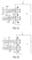
- la figure 1 est un schéma pour illustrer un exemple de réalisation d'un circuit selon l'invention, selon deux configurations d'applications, illustrées aux figures 1A et 1B,
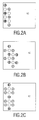
- la figure 2 est un schéma pour illustrer trois autres exemples de réalisation de l'invention, illustrés aux figures 2A, 2B et 2C, respectivement.
- FIG. 1 is a diagram for illustrating an exemplary embodiment of a circuit according to the invention, according to two application configurations, illustrated in FIGS. 1A and 1B,
- Figure 2 is a diagram to illustrate three other embodiments of the invention, illustrated in Figures 2A, 2B and 2C, respectively.
Dans des applications utilisant des circuits intégrés fonctionnant à haut débit, telles que les transmissions optiques, les signaux transmis sont de type différentiels. Ils sont couramment représentés par des signaux complémentaires, appelés composantes I et IQ du signal différentiel lorsqu'il s'agit de signaux entrant et composantes O et OQ lorsqu'il s'agit de signaux sortant. Les exemples illustrés dans les figures 1 et 2 concernent des signaux entrant mais l'invention s'applique également en sortie des circuits, aux jeux de connexions délivrant les signaux sortant. Les deux composantes I et IQ du signal différentiel sont véhiculées sur deux fils simultanément. La différence entre les deux composantes du signal peut par exemple être assimilée à une suite de données numériques binaires de type "0" ou "1".In applications using integrated circuits operating at high speed, such as optical transmissions, the signals transmitted are of the differential type. They are commonly represented by complementary signals, called components I and IQ of the differential signal when it comes to incoming signals and O and OQ components when it comes to outgoing signals. The examples illustrated in Figures 1 and 2 relate to incoming signals but the invention also applies at the output of the circuits, to sets of connections delivering the outgoing signals. The two components I and IQ of the differential signal are carried on two sons simultaneously. The difference between the two components of the signal can for example be assimilated to a series of binary digital data of type "0" or "1".
La figure 1 montre un exemple de réalisation préféré d'un circuit intégré selon l'invention, noté IC, connecté à une première et une deuxième lignes de transmission différentielles parallèles, notées S1 et S2 respectivement. L'invention est applicable de façon identique à une seule ligne de transmission. La présence d'une ou de deux lignes S1 et S2 et des plots de connexion associés sur les figures 1 à 3, est destinée à montrer comment plusieurs lignes peuvent être connectées à l'aide d'un dispositif selon l'invention. La première ligne S1 se décompose en une première composante, notée S1I, et une deuxième composante, notée S1IQ. La deuxième ligne S2 se décompose en une première composante, notée S2I et une deuxième composante, notée S2IQ. Chaque composante I ou IQ du signal différentiel comporte à son tour deux voies distinctes comprenant une première voie ou ligne directe transportant le signal utile à transmettre et une deuxième voie ou ligne de retour portée à une tension de référence dépendant de l'application.FIG. 1 shows a preferred embodiment of an integrated circuit according to the invention, denoted IC, connected to first and second transmission lines parallel differentials, denoted S1 and S2 respectively. The invention is applicable in a way identical to a single transmission line. The presence of one or two lines S1 and S2 and connection pads associated in Figures 1 to 3, is intended to show how several lines can be connected using a device according to the invention. The first line S1 is breaks down into a first component, denoted S1I, and a second component, denoted S1IQ. The second line S2 is broken down into a first component, denoted S2I and a second component, denoted S2IQ. Each I or IQ component of the differential signal has in turn two separate routes including a first route or direct line carrying the useful signal to transmit and a second return channel or line brought to a voltage of reference depending on the application.
Les lignes différentielles transportent les composantes I et IQ des signaux
différentiels à transmettre. Elles sont matérialisées par des pistes réalisées avec un matériau
conducteur tracées ou imprimées sur un support en matériau isolant. L'ensemble des pistes
tracées forme un circuit, couramment appelé circuit imprimé ou PCB, destiné à interconnecter
des circuits intégrés (un seul circuit intégré est représenté sur la figure 1) selon un routage
prédéterminé en fonction de l'application envisagée. Les circuits intégrés sont généralement
situés à l'intérieur de boítiers 1 réalisés en matériau isolant. Les connexions entre les lignes
imprimées et les circuits intégrés sont réalisées au moyen d'un jeu de plots de connexions,
représentés sur la figure par des cercles. Dans le cas où le circuit est intégré dans un boítier de
type BGA (de l'anglais Ball Gate Array) les plots de connexion sont pratiquement sphériques et
sont appelés des balles de connexion. Le jeu de plots de connexions comporte des connexions
destinées à recevoir les signaux différentiels à transmettre, dits plots de signal et des
connexions destinées à l'alimentation des circuits, dits plots d'alimentation. L'alimentation se fait
à l'aide de deux tensions d'alimentation distinctes, l'une étant supérieure à l'autre et l'une
correspond généralement à la masse. Les plots d'alimentation sont donc soumis à une tension
de référence parmi deux tensions de référence distinctes possibles, l'une dite référence haute et
l'autre dite référence basse. Les plots d'alimentation sont représentées par des cercles
hachurés. Par convention, sur la figure 1, les hachures verticales correspondent aux plots reliés
à la référence basse et les hachures en biais correspondent aux plots reliés à la référence
haute.Differential lines carry I and IQ components of signals
differentials to be transmitted. They are materialized by tracks made with a material
conductor traced or printed on a support of insulating material. All tracks
traces form a circuit, commonly called a printed circuit or PCB, intended to interconnect
integrated circuits (a single integrated circuit is shown in FIG. 1) according to a routing
predetermined according to the intended application. Integrated circuits are generally
located inside
Deux configurations d'alimentation sont alors possibles pour le circuit intégré. Selon une première configuration, dite configuration positive, la tension de référence basse correspond à la masse et la tension de référence haute correspond à une tension constante positive, notée + VCC. Selon la deuxième configuration, dite configuration négative, la tension de référence basse correspond à une tension constante négative, notée -VCC et la tension de référence haute correspond à la masse. Les circuit intégrés peuvent donc être alimentés selon l'une ou l'autre de ces configurations au choix. En revanche, l'application envisagée n'a en général qu'une seule tension de référence, par exemple la masse. Dans ce cas, il est préférable que les lignes de retour des lignes différentielles soient reliées à la masse. Or, selon la configuration d'alimentation du circuit imprimé, la masse n'est pas reliée aux mêmes plots de connexions, ce qui implique que le traçage des pistes imprimées peut être différent d'une configuration à l'autre comme le montrent les figures 1A et 1B.Two supply configurations are then possible for the integrated circuit. According to a first configuration, called positive configuration, the low reference voltage corresponds to ground and the high reference voltage corresponds to a constant voltage positive, denoted + VCC. According to the second configuration, called negative configuration, the voltage of low reference corresponds to a negative constant voltage, noted -VCC and the voltage of high reference corresponds to the mass. The integrated circuits can therefore be supplied according to either of these configurations. On the other hand, the envisaged application did not generally only one reference voltage, for example ground. In this case, it is better that the return lines of the differential lines are connected to ground. However, according to the power supply configuration of the printed circuit, the earth is not connected to the same pads connections, which implies that the tracing of the printed tracks can be different from a configuration to the other as shown in Figures 1A and 1B.
La figure 1A illustre un exemple de réalisation d'un circuit selon l'invention dans la configuration positive. La figure 1B illustre le même circuit selon la configuration négative. Les plots de signal, représentés sur les figures 1A et 1B par des cercles non hachurés, sont situées en bordure du boítier et sont entourés par les plots d'alimentation qui recoivent des tensions de référence constantes. De préférence, la disposition des paires de plots de connexion est symétrique par rapport à un plan perpendiculaire au plan du PCB et perpendiculaire au coté du boítier le plus proche du jeu de plots de connexions considérées. Cette disposition des plots de connexion est compatible avec les deux configurations d'alimentation possibles. Dans chaque configuration, les lignes de transmission directes ainsi que les plots de signal auxquelles elles sont connectées sont encadrées par la masse ou l'alimentation, selon la configuration utilisée, formant ainsi un écran de protection contre d'éventuelles perturbations électromagnétiques générées par les signaux transmis à haute fréquence.FIG. 1A illustrates an exemplary embodiment of a circuit according to the invention in the positive configuration. FIG. 1B illustrates the same circuit according to the negative configuration. The signal pads, represented in FIGS. 1A and 1B by unhatched circles, are located on the edge of the housing and are surrounded by the supply studs which receive constant reference voltages. Preferably, the arrangement of the pairs of connection pads is symmetrical with respect to a plane perpendicular to the PCB plane and perpendicular to the side of the box closest to the set of connection pads considered. This arrangement of the studs connection is compatible with the two possible power supply configurations. In each configuration, the direct transmission lines and the signal pads to which they are connected are surrounded by earth or power, depending on the configuration used, thus forming a protective screen against possible electromagnetic interference generated by signals transmitted at high frequency.
Le dispositif illustré aux figures 1A et 1B présente de nombreux avantages. Un premier avantage est la facilité d'accès des plots de signal. Les plots de signal sont disposés au bord du boítier pour permettre un accès direct aux lignes de transmission. Un deuxième avantage est la symétrie du dispositif. Les plots de connexion sont disposés sur le boítier de façon symétrique par rapport à un plan perpendiculaire au plan du circuit intégré et passant parallèlement aux lignes de transmission par un point milieu séparant lesdites lignes de transmission. Ce qui signifie que les distances parcourues par le signal peuvent être les mêmes sur chaque composante différentielle complémentaire SI et SIQ de la ligne de transmission, avec tous les avantages bien connus que cela implique. Un troisième avantage est la qualité du blindage. Chaque paire de lignes de transmission est encadrée jusqu'au plot de signal par deux lignes de référence propres, non bruitées, ce qui favorise une bonne transmission des signaux.The device illustrated in Figures 1A and 1B has many advantages. A first advantage is the ease of access of the signal pads. The signal pads are arranged at the edge of the box to allow direct access to transmission lines. A second advantage is the symmetry of the device. The connection pads are arranged on the housing of symmetrically with respect to a plane perpendicular to the plane of the integrated circuit and passing parallel to the transmission lines by a midpoint separating said transmission lines transmission. This means that the distances traveled by the signal can be the same on each complementary differential component SI and SIQ of the transmission line, with all the well-known benefits that this entails. A third advantage is the quality of the shielding. Each pair of transmission lines is framed to the signal pad by two clean reference lines, not noisy, which promotes good signal transmission.
La figure 2 montre trois autres exemples de réalisation de l'invention. Ces trois exemples sont donnés à titre indicatif et non restrictif. Ils peuvent donner lieu à de nombreuses variantes sans sortir du cadre de l'invention. Les éléments communs avec la figure 1 portent les mêmes références.FIG. 2 shows three other exemplary embodiments of the invention. These three examples are given for information only and are not restrictive. They can give rise to many variants without departing from the scope of the invention. The elements common with Figure 1 bear the same references.
La figure 2A illustre une variante dans laquelle les plots de signal sont disposés sur deux rangées parallèles au coté du boítier décalées en quinconce pour en limiter l'encombrement. Les plots d'alimentation sont disposés autour et entre les plots de signal sur les mêmes rangées parallèles. En revanche, ce mode de réalisation n'est pas symétrique et l'accès aux signaux est moins direct que dans le mode de réalisation illustré à la figure 1.FIG. 2A illustrates a variant in which the signal pads are arranged in two rows parallel to the side of the case staggered to limit clutter. The power pads are arranged around and between the signal pads on the same parallel rows. However, this embodiment is not symmetrical and access to signals is less direct than in the embodiment illustrated in FIG. 1.
La figure 2B illustre une autre variante de réalisation. Selon cette variante, les plots de signal sont toujours disposés en quinconce sur deux rangées parallèles mais les plots d'alimentation sont disposés sur quatre rangées parallèles et notamment entre les plots de signal sur les deux rangées de plots de signal, de sorte que chaque plot de signal est entouré aux quatre cotés par au moins un plot d'alimentation. Ce mode de réalisation permet également de limiter l'encombrement des plots de connexion et donc d'en disposer un plus grand nombre sur le boítier. Il permet également d'ajouter de façon simple d'autres rangées ou couches de plots de connexion vers le centre du boítier. En revanche, ce mode de réalisation n'est pas symétrique. FIG. 2B illustrates another alternative embodiment. According to this variant, the signal pads are always staggered in two parallel rows but the pads supply are arranged in four parallel rows and in particular between the pads signal on the two rows of signal pads, so that each signal pad is surrounded on all four sides by at least one power pad. This embodiment also allows limit the size of the connection pads and therefore have a larger number on the housing. It also allows you to easily add other rows or layers of connection pads to the center of the case. However, this embodiment is not symmetrical.
La figure 2C illustre encore une autre variante de réalisation. Selon cette variante, les plots de signal sont disposés par paires successives séparées par au moins un plot d'alimentation sur une même rangée parallèle au coté du boítier. Les autres plots d'alimentation sont disposés de part et d'autre de la rangée de plots de signal de façon à entourer chaque paire de plots de signal. Ce mode de réalisation a l'avantage d'être symétrique et d'offrir un bon blindage des lignes de transmission mais il est plus encombrant que les mode de réalisation précédents.FIG. 2C illustrates yet another alternative embodiment. According to this variant, the signal pads are arranged in successive pairs separated by at least one pad supply on the same row parallel to the side of the housing. The other power pads are arranged on either side of the row of signal pads so as to surround each pair of signal pads. This embodiment has the advantage of being symmetrical and of offering a good shielding of transmission lines but it is more cumbersome than the embodiments precedents.
On a ainsi décrit et illustré à l'aide d'exemples un circuit intégré selon l'invention dans une application impliquant une paire de lignes de transmission différentielles. D'autres variantes de réalisation pourront être envisagées en fonction de l'application considérée sans sortir du cadre de l'invention, notamment en ce qui concerne la position respective et le nombre des plots de connexion sur le boítier du circuit intégré.An integrated circuit according to the invention has thus been described and illustrated with the aid of examples. in an application involving a pair of differential transmission lines. other alternative embodiments may be envisaged depending on the application considered without depart from the scope of the invention, in particular as regards the respective position and the number connection pads on the case of the integrated circuit.
Claims (9)
Applications Claiming Priority (2)
| Application Number | Priority Date | Filing Date | Title |
|---|---|---|---|
| FR0114664 | 2001-11-13 | ||
| FR0114664 | 2001-11-13 |
Publications (2)
| Publication Number | Publication Date |
|---|---|
| EP1310995A2 true EP1310995A2 (en) | 2003-05-14 |
| EP1310995A3 EP1310995A3 (en) | 2010-10-20 |
Family
ID=8869341
Family Applications (1)
| Application Number | Title | Priority Date | Filing Date |
|---|---|---|---|
| EP02079626A Withdrawn EP1310995A3 (en) | 2001-11-13 | 2002-11-06 | Device for shielding the signal lines by the ground or power lines |
Country Status (6)
| Country | Link |
|---|---|
| US (1) | US6791165B2 (en) |
| EP (1) | EP1310995A3 (en) |
| JP (1) | JP4454926B2 (en) |
| KR (1) | KR20030040071A (en) |
| CN (1) | CN1331225C (en) |
| TW (1) | TW200408091A (en) |
Cited By (2)
| Publication number | Priority date | Publication date | Assignee | Title |
|---|---|---|---|---|
| WO2015146738A1 (en) * | 2014-03-24 | 2015-10-01 | 技術研究組合光電子融合基盤技術研究所 | Pad-array structure on substrate for mounting ic chip on substrate, and optical module having said pad-array structure |
| WO2018209003A1 (en) * | 2017-05-10 | 2018-11-15 | Qualcomm Incorporated | Connector for differential routing |
Families Citing this family (19)
| Publication number | Priority date | Publication date | Assignee | Title |
|---|---|---|---|---|
| US6700181B1 (en) * | 2002-11-19 | 2004-03-02 | Inphi Corporation | Method and system for broadband transition from IC package to motherboard |
| US20070262448A1 (en) * | 2004-08-20 | 2007-11-15 | Tsutomu Ishino | Semiconductor Device, Power Supply Apparatus Using Same, and Electronic Device |
| US7294976B1 (en) | 2005-09-23 | 2007-11-13 | Advanced Micro Devices, Inc. | Split power supply subsystem with isolated voltage supplies to satisfy a predetermined power limit |
| JP4595823B2 (en) * | 2006-01-24 | 2010-12-08 | 株式会社デンソー | Ball grid array |
| JP5336700B2 (en) * | 2006-11-30 | 2013-11-06 | ローム株式会社 | Semiconductor device and electronic apparatus using the same |
| JP5034095B2 (en) * | 2007-07-13 | 2012-09-26 | 株式会社リコー | Printed wiring board and electronic device |
| JP2010010492A (en) * | 2008-06-27 | 2010-01-14 | Sony Corp | Semiconductor device and semiconductor integrated circuit |
| JP5028357B2 (en) * | 2008-08-07 | 2012-09-19 | キヤノン株式会社 | Differential transmission circuit |
| US8310276B2 (en) | 2008-06-27 | 2012-11-13 | Canon Kabushiki Kaisha | Differential transmission circuit |
| KR100951667B1 (en) * | 2008-08-19 | 2010-04-07 | 주식회사 하이닉스반도체 | Semiconductor Memory Device Having Pads |
| TWI407421B (en) | 2009-02-17 | 2013-09-01 | Au Optronics Corp | Driving apparatus for driving a liquid crystal display panel |
| CN101494040B (en) * | 2009-03-06 | 2013-05-08 | 友达光电股份有限公司 | Drive device for driving liquid crystal display panel |
| JP5351063B2 (en) | 2010-01-13 | 2013-11-27 | 株式会社アドバンテスト | Contact device and circuit package |
| JP5416269B2 (en) * | 2012-12-11 | 2014-02-12 | 古河電気工業株式会社 | Parallel optical transmission equipment |
| JP2015153808A (en) * | 2014-02-12 | 2015-08-24 | ソニー株式会社 | Semiconductor chip and semiconductor module |
| JP6527420B2 (en) * | 2015-07-31 | 2019-06-05 | ルネサスエレクトロニクス株式会社 | Semiconductor device |
| WO2018042518A1 (en) * | 2016-08-30 | 2018-03-08 | 株式会社日立製作所 | Semiconductor device and printed circuit board |
| TWI684245B (en) * | 2018-08-29 | 2020-02-01 | 財團法人工業技術研究院 | Differential signal transmitting circuit board |
| KR20230031532A (en) | 2021-08-27 | 2023-03-07 | 삼성전자주식회사 | Memory device and method for operating the same |
Citations (7)
| Publication number | Priority date | Publication date | Assignee | Title |
|---|---|---|---|---|
| US5331514A (en) * | 1991-08-05 | 1994-07-19 | Ngk Spark Plug Co., Ltd. | Integrated-circuit package |
| US5686764A (en) * | 1996-03-20 | 1997-11-11 | Lsi Logic Corporation | Flip chip package with reduced number of package layers |
| US5714801A (en) * | 1995-03-31 | 1998-02-03 | Kabushiki Kaisha Toshiba | Semiconductor package |
| US5796170A (en) * | 1996-02-15 | 1998-08-18 | Northern Telecom Limited | Ball grid array (BGA) integrated circuit packages |
| US5994766A (en) * | 1998-09-21 | 1999-11-30 | Vlsi Technology, Inc. | Flip chip circuit arrangement with redistribution layer that minimizes crosstalk |
| JP2000349192A (en) * | 1999-06-07 | 2000-12-15 | Canon Inc | Semiconductor integrated circuit and printed wiring board |
| US6215184B1 (en) * | 1998-02-19 | 2001-04-10 | Texas Instruments Incorporated | Optimized circuit design layout for high performance ball grid array packages |
Family Cites Families (12)
| Publication number | Priority date | Publication date | Assignee | Title |
|---|---|---|---|---|
| GB2324649A (en) * | 1997-04-16 | 1998-10-28 | Ibm | Shielded semiconductor package |
| US6057600A (en) * | 1997-11-27 | 2000-05-02 | Kyocera Corporation | Structure for mounting a high-frequency package |
| US6373447B1 (en) * | 1998-12-28 | 2002-04-16 | Kawasaki Steel Corporation | On-chip antenna, and systems utilizing same |
| US6329702B1 (en) * | 2000-07-06 | 2001-12-11 | Tyco Electronics Corporation | High frequency carrier |
| US6563299B1 (en) * | 2000-08-30 | 2003-05-13 | Micron Technology, Inc. | Apparatus for measuring parasitic capacitance and inductance of I/O leads on an electrical component using a network analyzer |
| US20020113309A1 (en) * | 2001-01-04 | 2002-08-22 | Siamak Fazelpour | Shielding of RF devices |
| JP4536942B2 (en) * | 2001-02-09 | 2010-09-01 | 三菱電機株式会社 | High-frequency integrated circuit and high-frequency circuit device using the same |
| JP4623850B2 (en) * | 2001-03-27 | 2011-02-02 | 京セラ株式会社 | High frequency semiconductor element storage package and its mounting structure |
| JP2003068928A (en) * | 2001-08-28 | 2003-03-07 | Kyocera Corp | Mounting structure of wiring board for high frequency |
| US6603193B2 (en) * | 2001-09-06 | 2003-08-05 | Silicon Bandwidth Inc. | Semiconductor package |
| US6635958B2 (en) * | 2001-12-03 | 2003-10-21 | Dover Capital Formation Group | Surface mount ceramic package |
| US20030198032A1 (en) * | 2002-04-23 | 2003-10-23 | Paul Collander | Integrated circuit assembly and method for making same |
-
2002
- 2002-11-01 TW TW091132393A patent/TW200408091A/en unknown
- 2002-11-06 EP EP02079626A patent/EP1310995A3/en not_active Withdrawn
- 2002-11-07 JP JP2002323857A patent/JP4454926B2/en not_active Expired - Fee Related
- 2002-11-08 CN CNB021499233A patent/CN1331225C/en not_active Expired - Fee Related
- 2002-11-08 US US10/291,035 patent/US6791165B2/en not_active Expired - Lifetime
- 2002-11-08 KR KR1020020069137A patent/KR20030040071A/en not_active Application Discontinuation
Patent Citations (7)
| Publication number | Priority date | Publication date | Assignee | Title |
|---|---|---|---|---|
| US5331514A (en) * | 1991-08-05 | 1994-07-19 | Ngk Spark Plug Co., Ltd. | Integrated-circuit package |
| US5714801A (en) * | 1995-03-31 | 1998-02-03 | Kabushiki Kaisha Toshiba | Semiconductor package |
| US5796170A (en) * | 1996-02-15 | 1998-08-18 | Northern Telecom Limited | Ball grid array (BGA) integrated circuit packages |
| US5686764A (en) * | 1996-03-20 | 1997-11-11 | Lsi Logic Corporation | Flip chip package with reduced number of package layers |
| US6215184B1 (en) * | 1998-02-19 | 2001-04-10 | Texas Instruments Incorporated | Optimized circuit design layout for high performance ball grid array packages |
| US5994766A (en) * | 1998-09-21 | 1999-11-30 | Vlsi Technology, Inc. | Flip chip circuit arrangement with redistribution layer that minimizes crosstalk |
| JP2000349192A (en) * | 1999-06-07 | 2000-12-15 | Canon Inc | Semiconductor integrated circuit and printed wiring board |
Cited By (4)
| Publication number | Priority date | Publication date | Assignee | Title |
|---|---|---|---|---|
| WO2015146738A1 (en) * | 2014-03-24 | 2015-10-01 | 技術研究組合光電子融合基盤技術研究所 | Pad-array structure on substrate for mounting ic chip on substrate, and optical module having said pad-array structure |
| JPWO2015146738A1 (en) * | 2014-03-24 | 2017-04-13 | 技術研究組合光電子融合基盤技術研究所 | Pad array structure on substrate for mounting IC chip on substrate, and optical module having said pad array structure |
| US9775245B2 (en) | 2014-03-24 | 2017-09-26 | Photonics Electronics Technology Research Association | Pad-array structure on substrate for mounting IC chip on substrate, and optical module having said pad-array structure |
| WO2018209003A1 (en) * | 2017-05-10 | 2018-11-15 | Qualcomm Incorporated | Connector for differential routing |
Also Published As
| Publication number | Publication date |
|---|---|
| JP2003249904A (en) | 2003-09-05 |
| KR20030040071A (en) | 2003-05-22 |
| JP4454926B2 (en) | 2010-04-21 |
| US20030102536A1 (en) | 2003-06-05 |
| US6791165B2 (en) | 2004-09-14 |
| EP1310995A3 (en) | 2010-10-20 |
| CN1419287A (en) | 2003-05-21 |
| CN1331225C (en) | 2007-08-08 |
| TW200408091A (en) | 2004-05-16 |
Similar Documents
| Publication | Publication Date | Title |
|---|---|---|
| EP1310995A2 (en) | Device for shielding the signal lines by the ground or power lines | |
| Doany et al. | Terabit/sec VCSEL-based 48-channel optical module based on holey CMOS transceiver IC | |
| FR2695272A1 (en) | Mixer circuit for radio or television signals. | |
| JP7095583B2 (en) | Optical transmitter | |
| JP6988322B2 (en) | Package for optical receiver module | |
| JP6448045B2 (en) | Opto-electric integrated circuit and optical interposer | |
| FR2735324A1 (en) | Multi-layer circuit wiring board for data processing equipment | |
| FR2670589A1 (en) | INTEGRATED ELECTROOPTIC MODULATION DEVICE. | |
| JP2007266251A (en) | Optical semiconductor device | |
| FR3071932B1 (en) | SWITCHES AND INTEGRATED PHOTONIC INTERCONNECTION NETWORK IN AN OPTOELECTRONIC CHIP | |
| EP0346206A1 (en) | Active connector for printed-circuit boards | |
| US7917042B2 (en) | High speed optoelectronic receiver | |
| FR3074402B1 (en) | MASS LOOP SYSTEM INTEGRATING AN ELECTRIC COUPLING DEVICE ACTING ON A PARASITIC CURRENT | |
| EP0596568A1 (en) | Semiconductor device comprising a monolithic integrated distribited amplifier circuit with wide bandwidth and high gain | |
| JP3269654B2 (en) | Optoelectronic transceiver | |
| EP3402096B1 (en) | Compact fsoi module capable of withstanding harsh environments | |
| JP2009026826A (en) | Optical transmitting and receiving module | |
| EP0606943B1 (en) | Switching device for switching television signals in a cable distribution system | |
| WO2024009388A1 (en) | Light receiver | |
| JP2020079850A (en) | Optical transmitter-receiver | |
| JP2019101140A (en) | Optical modulator and optical transmission device using the same | |
| JPH04119697A (en) | Signal transmission method between plug-in units | |
| FR2579022A1 (en) | ELECTRONIC CIRCUIT ASSEMBLY COMPRISING AT LEAST ONE INTEGRATED CIRCUIT ELEMENT | |
| KR100699569B1 (en) | The package structure for bi-directional optical modules | |
| EP0533549B1 (en) | Impedance matching device for transmission lines between one or more transmitters and one or more receivers of signals |
Legal Events
| Date | Code | Title | Description |
|---|---|---|---|
| PUAI | Public reference made under article 153(3) epc to a published international application that has entered the european phase |
Free format text: ORIGINAL CODE: 0009012 |
|
| AK | Designated contracting states |
Designated state(s): AT BE BG CH CY CZ DE DK EE ES FI FR GB GR IE IT LI LU MC NL PT SE SK TR |
|
| AX | Request for extension of the european patent |
Extension state: AL LT LV MK RO SI |
|
| RAP1 | Party data changed (applicant data changed or rights of an application transferred) |
Owner name: NXP B.V. |
|
| PUAL | Search report despatched |
Free format text: ORIGINAL CODE: 0009013 |
|
| AK | Designated contracting states |
Kind code of ref document: A3 Designated state(s): AT BE BG CH CY CZ DE DK EE ES FI FR GB GR IE IT LI LU MC NL PT SE SK TR |
|
| AX | Request for extension of the european patent |
Extension state: AL LT LV MK RO SI |
|
| 17P | Request for examination filed |
Effective date: 20110411 |
|
| AKX | Designation fees paid |
Designated state(s): AT BE BG CH CY CZ DE DK EE ES FI FR GB GR IE IT LI LU MC NL PT SE SK TR |
|
| 17Q | First examination report despatched |
Effective date: 20110825 |
|
| STAA | Information on the status of an ep patent application or granted ep patent |
Free format text: STATUS: THE APPLICATION IS DEEMED TO BE WITHDRAWN |
|
| 18D | Application deemed to be withdrawn |
Effective date: 20150922 |