Technical Field of the Invention
-
The present invention relates to a semiconductor device
such as an IC chip, a semiconductor device manufacturing method,
a multilayer printed circuit board into which a semiconductor
device is integrated and a multilayer printed circuit board
manufacturing method.
Background of the Invention
-
An IC chip is electrically connected to a printed circuit
board by a mounting method such as wire bonding, TAB or flip
chip bonding.
-
In the wire bonding method, an IC chip is die-bonded to
a printed circuit board by adhesive, the pads of the printed
circuit board are connected to the pads of an IC chip by wires
such as metallic wires and then a sealing resin such as a
thermosetting resin or a thermoplastic resin is applied to
protect the IC chip and the wires.
-
In the TAB method, the wires referred to as leads are
connected in the block by a solder or the like and then the bumps
of an IC chip and the pads of a printed circuit board are sealed
by a resin.
-
In the flip chip bonding method, the pads of an IC chip
are connected to the pads of a printed circuit board through
bumps and the gaps'between the pads and the bumps are filled
with a resin.
-
In each of these mounting methods, however, the IC chip
is electrically connected to the printed circuit board through
connection lead members (wires, leads or bumps). The lead
members tend to be cut off and eroded, thereby breaking the
connection of the printed circuit board with the IC chip and
causing malfunctions.
-
Further, in each mounting method, a thermoplastic resin
such as an epoxy resin is applied to seal the IC chip so as to
protect the IC chip. If bubbles are contained at the time of
filling the resin, the breakage of lead members, the corrosion
of the IC pads and the deterioration of reliability are derived
from the bubbles. To seal members by a thermoplastic resin,
it is necessary to create resin filling plungers and metallic
molds in accordance with the respective members. In addition,
if a thermosetting resin is employed, it is necessary to select
an appropriate resin for the materials of lead members, solder
resist and the like, thereby disadvantageously causing cost
increase.
-
On the other hand, there has been conventionally proposed
a technique for electrically connecting an IC chip to a printed
circuit board by embedding a semiconductor device into a
substrate and forming buildup layers on the substrate instead
of attaching the IC chip to the exterior of the printed circuit
board (or package substrate) as stated above in Japanese Patent
Laid-Open Nos. 9-321408 (or USP5875100), 10-256429, 11-126978
and the like.
-
According to Japanese Patent Laid-Open No. 9-321408 (or
USP5875100), a semiconductor device having stud bumps formed
on die pads is embedded into a printed circuit board and wirings
are formed on the stud bumps to thereby electrically connect
the printed circuit board to the semiconductor device. However,
since the stud bumps are onion-shaped and irregular in height,
smoothness is deteriorated if an interlayer insulating layer
is formed and electrical connection cannot be established even
if via holes are formed. Further, since the stud bumps are
provided by bonding one by one, they cannot be provided
collectively and productivity is thereby disadvantageously
lowered.
-
Japanese Patent Laid-Open No. 10-256429 shows a structure
in which a semiconductor device is contained in a ceramic
substrate and the substrate is electrically connected to the
semiconductor device by flip chip bonding. However, ceramic
is inferior in outline workability and the semiconductor device
cannot be appropriately contained in the ceramic substrate.
Besides, the bumps are irregular in height. Due to this, the
smoothness of an interlayer insulating layer is deteriorated
and connection characteristic is deteriorated accordingly.
-
Japanese Patent Laid-Open No.11-126978 shows amultilayer
printed circuit board wherein an electrical component such as
a semiconductor device is embedded into a gap or containing
portion, connected to a conductor circuit and built up through
via holes. However, since the containing portion is a gap, a
positional error tends to occur and the substrate cannot be often
connected to the pads of the semiconductor device. Besides,
since die pads are directly connected to the conductor circuit,
oxide coats tend to be formed on the respective die pads, thereby
disadvantageously increasing insulating resistance.
-
The present invention has been made to improve the
above-stated problems. It is an object of the present invention
to provide a semiconductor device manufacturing method which
allows a semiconductor device to be directly electrical connected
to a printed circuit board without using lead members.
-
Meanwhile, if a semiconductor device is embedded into a
printed circuit board made of resin, then the printed circuit
board is warped by heat generated in the semiconductor device,
internal wirings are cut off and reliability is thereby
disadvantageously deteriorated.
-
The present invention has been made to improve the
above-stated problem. It is, therefore, a still further object
of the present invention to provide a multilayer printed circuit
board into which a semiconductor device is integrated and the
method of manufacturing the multilayer printed circuit board.
-
Furthermore, conventionally, a highly reliable printed
circuit board into which a semiconductor device is integrated
cannot be efficiently manufactured.
-
The present invention has been made to improve the above
problem. It is, therefore, a still further object of the present
invention to provide a manufacturing method capable of
efficiently manufacturing a highly reliable multilayer printed
circuit board into which a semiconductor device is integrated.
-
Moreover, if a multilayer printed circuit board comprising
a substrate into which a semiconductor device is embedded and
contained, is employed as a package substrate, a chip set or
the like, the multilayer printed circuit board can fulfill its
behaviors by being electrically connected to an external
substrate (which is a so-called mother board or a daughter board).
Due to this, it is necessary to provide BGA's and conductive
connection pins (PGA's) on the multilayer printed circuit board.
The BGA's and PGA's are formed by providing solder pads on a
solder resist layer on the surface layer of the multilayer printed
circuit board.
-
However, if a behavioral test or a reliability test is
conducted while providing solder bumps on the surface layer of
a substrate into which a semiconductor device is embedded and
electrically connecting the substrate to an external substrate,
it is discovered that an interlayer insulating layer, a solder
resist layer, an interlayer resin insulating layer, a solder
resist, solder bumps and the surroundings of the solder bumps
(which means solder layers and corrosion resisting metal) are
cracked and peeled, that the solder bumps are detached and that
the positions of the solder bumps are slipped. Particularly,
cracks occur to the pads of the semiconductor device and the
cracks penetrate the interlayer insulating layer. Accordingly,
it becomes clear that in the multilayer printed circuit board
into which the semiconductor device is integrated, the electrical
connection characteristics between solder bumps and conductor
circuits is disadvantageously deteriorated and that the
reliability of the multilayer printed circuit board is
deteriorated accordingly.
-
The present invention has been made to improve the
above-stated problems. It is, therefore, a still further object
of the present invention to provide a multilayer printed circuit
board or particularly a multilayer printed circuit board into
which a semiconductor device is integrated having high electrical
connection characteristics and high reliability.
Disclosure of the Invention
-
As a result of dedicated studies, the inventor of the
present invention devised to form a transition layer on the die
pad of a semiconductor device. Even if the semiconductor device
having the transition layer is embedded, stored and contained
in a printed circuit board and an interlayer insulating layer
is provided on the semiconductor device and via holes are formed
in the interlayer insulating layer, it is possible to obtain
desired size and shape.
-
The reason for providing the transition layer on the die
pad of an IC chip will be described. The die pad of an IC chip
is normally made of aluminum or the like. If the via holes of
an interlayer insulating layer are formed by photo-etching while
no transition layer is formed on the die pad, a resin tends to
remain on the surface layer of the pad after exposure and
development. Besides, the pad is discolored due to the adhesion
of a development solution. On the other hand, if via holes are
formed by laser, there is a possibility of burning the aluminum
pad. Also, if via holes are formed under the conditions that
the pad is not burned, a resin residue on the pad occurs. In
addition, if the IC chip is immersed in an acid, an oxidizer
or an etching solution in later steps or subjected to various
annealing steps, the pad of the IC chip is discolored and dissolved.
Moreover, the pad of the IC chip is formed to have a diameter
of about 40 µm and a via hole is larger in diameter than the
pad to thereby require a location tolerance. As a result, a
positional error and a connection defect tend to occur.
-
By providing a transition layer made of copper or the like
on a die pad, by contrast, a via hole formation defect can be
improved to make it possible to use a solvent and a resin residue
on the pad can be prevented. Also, even if the IC chip is immersed
in an oxide, an oxidizer or an etching solution in later steps
or subjected to various annealing steps, the pad is not discolored
or dissolved. This allows improving the connection
characteristics between the pad and the via hole and reliability.
Moreover, by interposing the transition layer having a larger
diameter than that of the die pad of the IC chip, it is possible
to ensure connecting the via hole to the pad. It is preferable
that the transition layer is equal to or larger than a via hole
diameter or a location tolerance.
-
Furthermore, since the transition layer is formed, the
operation test and electrical test of the semiconductor device
can be easily conducted before or after embedding, containing
and storing the IC chip which is a semiconductor device in a
printed circuit board. This is because the transition layer
larger than the pad is formed and a test probe pin can be contacted
with the IC chip more easily. As a result, it is possible to
determine whether a product is good or defective in advance and
to improve productivity and cost effectiveness. Besides, the
pad is not lost or damaged by the probe.
-
Thus, by forming the transition, the IC chip which is a
semiconductor device can be appropriately embedded, contained
and stored in the printed circuit board. Namely, the
semiconductor device having the transition layer may be also
referred to as a semiconductor device for embedding, containing
and storing the printed circuit board.
-
The transition layer is constituted by forming a thin film
layer on the die pad and a thickening layer on the thin film
layer. The transition layer can be formed to comprise at least
two layers.
-
The multilayer printed circuit board functions per se.
In some cases, BGA's, solder bumps or PGA's (conductive
connection pins) may be provided to connect the multilayer
printed circuit board to a mother board or a daughter board serving
as an external substrate so that the multilayer printed circuit
board functions as a package substrate for a semiconductor device.
In addition, with this constitution, wiring lengths can be
shortened and loop inductance can be reduced compared with a
case of connecting the multilayer printed circuit board to the
external substrate by a conventional mounting method.
-
Now, a transition layer defined in the present invention
will be described.
-
Since the transition layer directly connect an IC chip,
which is a semiconductor device, to a printed circuit board
without using a conventional IC chip mounting technique, the
transition layer signifies an intermediate layer. The
transition layer is characterized by being formed out of two
or more metallic layers or by being formed to be larger than
the die pad of the IC chip which is the semiconductor device.
This allows electrical connection characteristics and alignment
efficiency to be improved and processing a via hole by laser
or photo-etching without damaging the die pad. Due to this,
it is possible to ensure embedding, containing, storing and
connecting the IC chip in and to the printed circuit board.
Besides, it is possible to directly form a metal serving as the
conductor layer of the printed circuit board on the transition
layer. The conductor layer is exemplified by the via hole of
an interlayer resin insulating layer or a through hole on a
substrate.
-
As a resin substrate into which an electronic component
such as an IC chip used in the present invention is integrated,
a substrate containing an epoxy resin, a BT resin, a phenol resin
or the like impregnated with a reinforcement or a core material
such as a glass epoxy resin, or a substrate in which prepregs
impregnated with an epoxy resin are built up is used. Normally,
a substrate used for a printed circuit board is available.
Alternatively, a two-sided copper-clad laminated board, a
one-side board, a resin board without a metallic film or a resin
film can be used. However, if applied with heat at a temperature
of 350°C or higher, the resin is dissolved and carbonated.
-
Physical deposition such as deposition or sputtering is
conducted to the entire surface of the IC chip to thereby form
a conductive metallic film on the entire surface. The metallic
film is preferably formed of one or more layers of metal such
as tin, chromium, titanium, nickel, zinc, cobalt, goldor copper.
The thickness thereof is preferably in the range of 0.001 to
2.0 µm, more preferably in the range of 0.01 to 1.0 µm.
-
It is also possible to further provide a metallic film
on the metallic film by electroless plating or the like. The
upper metallic film is preferably formed out of one or more layers
of metal such as nickel, copper, gold or silver. The thickness
thereof is preferably 0.01 to 5.0 µm, more preferably 0.1 to
3.0 µm.
-
The metallic film is plated by electroless plating or
electroplating. The types of plating materials include nickel,
copper, gold, silver, zinc, iron and the like. In view of
electrical characteristics, inexpensiveness and the fact that
buildup conductor layers formed in later steps mainly comprise,
copper is preferably used. The thickness of the plated film
is preferably in the range of 1 to 20 µm. If the thickness exceeds
that range, undercut sometimes occurs during etching to thereby
generate gaps among the transition layers and via holes to be
formed, and interfaces. Thereafter, an etching resist is formed,
exposure and development are conducted and the metal other than
the transition layers are exposed and etching is conducted,
thereby forming a transition layer on each pad of the IC chip.
-
Further, instead of the above-stated transition layer
manufacturing method, it is also possible that a dry film resist
is formed on a metallic film formed on the IC chip and the core
substrate, a portion corresponding to the transition layer is
removed, a thickening layer is provided by electroplating, the
resist is peeled and that a transition layer is formed on each
pad of the IC chip by an etching solution.
-
As a result of devoted studies, the inventor of the present
invention discovered that by attaching a heat sink to the rear
surface of a semiconductor device embedded in a printed circuit
board, heat generated in the semiconductor device is discharged,
warping and breaking do not occur to the printed circuit board
and reliability can be obtained. Here, by forming a buildup
wiring out of a resin on the semiconductor device, it is possible
to appropriately connect the semiconductor device to the printed
circuit board.
-
It is preferable that the heat sink is connected to the
semiconductor device through a conductive adhesive. This is
because the conductive adhesive is high in heat conductivity
and is capable of efficiently discharging heat generated in the
semiconductor device toward the heat sink.
-
In addition, according to the present invention, prepregs
having a through hole containing therein the IC chip are built
up and pressurized vertically. An epoxy resin is exuded from
the prepregs and covers the upper surface of the IC chip. By
doing so, the upper surface of the IC chip and that of the core
substrate formed by curing the prepregs are completely flattened.
Due to this, at the time of forming buildup layers, via holes
and wirings can be appropriately formed and the wiring
reliability of the multilayer printed circuit board can be,
therefore, improved.
-
According to the present invention, a multilayer printed
circuit board provided with semiconductor devices is
manufactured for multiple multilayer printed circuit boards.
The multilayer printed circuit board is cut into pieces to thereby
obtain individual multilayer printed circuit boards. Due to
this, highly reliable multilayer printed circuit board can be
efficiently manufactured.
-
In addition, according to the present invention, prepregs
having a through hole containing therein the IC chip are built
up and pressurized vertically. An epoxy resin is exuded from
the prepregs and covers the upper surface of the IC chip. By
doing so, the upper surface of the IC chip and that of the core
substrate formed by curing a resin such as prepregs are completely
flattened. Due to this, at the time of forming buildup layers,
via holes and wirings can be appropriately formed and the wiring
reliability of the multilayer printed circuit board can be,
therefore, improved.
-
Furthermore, according to a preferred mode of the present
invention, a heat sink is attached to the rear surface of a
semiconductor device embedded into a printed circuit board. By
doing so, it is possible to discharge heat generated into the
semiconductor device, to prevent the occurrence of warping and
breaking of the printed circuit board and to improve reliability.
-
A method of manufacturing a multilayer printed circuit
board according to
claim 35 is characterized by comprising at
least the following steps (a) to (f):
- (a) attaching a sheet to a bottom of a through hole formed
in a core substrate;
- (b) mounting a semiconductor device on said sheet at the bottom
of said through hole so that a terminal contacts with said sheet;
- (c) filling a resin into said through hole;
- (d) pressurizing and curing said resin;
- (e) peeling of said sheet; and
- (f) forming a buildup layer on an upper surface of said
semiconductor device.
-
-
According to the invention recited in claim 35, the
semiconductor device is mounted on the sheet at the bottom of
the through hole of the core substrate so that the terminal
contacts with the sheet, the resin is filled into the through
hole and then the sheet is peeled, thereby forming a buildup
layer. That is to say, after mounting the semiconductor device
on the sheet so that the terminal thereof contacts with the sheet
and peeling the sheet, the buildup layer is formed on the
semiconductor device. Due to this, it is possible to
appropriately, electrically connect the terminal to the wiring
of the buildup layer and to, therefore, manufacture a highly
reliable multilayer printed circuit board into which the
semiconductor device is integrated.
-
A method of manufacturing a multilayer printed circuit
board according to
claim 36 is characterized by comprising at
least the following steps (a) to (i):
- (a) attaching a sheet to a bottom of a through hole formed
in a core substrate;
- (b) mounting said sheet on the bottom of said through hole
so that a terminal contacts with said sheet;
- (c) filling a resin into said through hole;
- (d) pressurizing and temporarily curing said resin;
- (e) peeling of said sheet;
- (f) polishing a bottom side of said core substrate, and
exposing the bottom of said semiconductor device;
- (g) actually curing said resin;
- (h) attaching a radiating plate to the bottom of said
semiconductor device; and
- (i) forming a buildup layer on an upper surface of said
semiconductor device.
-
-
According to the invention recited in claim 36, the
semiconductor device is mounted on the sheet at the bottom of
the through hole of the core substrate so that the terminal of
the device contacts with the sheet, the resin is filled into
the through hole and then the sheet is peeled, thereby forming
a buildup layer. That is to say, after mounting the semiconductor
device on the sheet so that the terminal thereof contacts with
the sheet and peeling the sheet, the buildup layer is formed
on the semiconductor device. Due to this, it is possible to
appropriately, electrically connect the terminal to the wiring
of the buildup layer and to, therefore, manufacture a highly
reliable multilayer printed circuit into which the semiconductor
device is integrated.
-
Furthermore, since the bottom side of the core substrate
is polished to exposure the bottom of the semiconductor device,
it is possible to attach a radiating plate to the bottom of the
semiconductor device and to, therefore, improve the stability
of the operation of the semiconductor device.
-
As a sheet closing the through hole of the core substrate,
a UV tape the viscosity of which is lowered if being applied
with UV is preferable. Since the UV tape is peeled without
leaving the adhesive on the terminal of the semiconductor device
by applying UV, it is possible to appropriately, electrically
connect the terminal to the wiring of the buildup layer and to,
therefore, manufacture a highly reliable multilayer printed
circuit board into which the semiconductor device is integrated.
-
It is also preferable to pressurize the resin under reduced
pressure. By reducing the pressure, no bubbles remain between
the core substrate and the resin and in the resin, thereby making
it possible to improve the reliability of the multilayer printed
circuit board.
-
It is further preferable to provide a taper on the through
hole formed in the core substrate. By providing the taper, no
bubbles or grooves remain between the through hole of the core
substrate and the resin and the reliability of the multilayer
printed circuit board can be improved. Besides, the smoothness
of the core substrate can be ensured.
-
In the invention recited in
claim 41, a multilayer printed
circuit board having interlayer insulating layers and conductor
layers repeatedly formed on a substrate in which a semiconductor
device is embedded, contained or stored, via holes formed in
said interlayer insulating layers, and establishing electrical
connection through said via holes, is characterized in that:
- an external connection terminal (BGA/PGA) is formed only
in a region in said substrate other than a region right above
the semiconductor device.
-
-
According to the invention recited in claim 41, the region
on the substrate of the multilayer printed circuit boar into
which region the semiconductor device is integrated and the
region on the substrate into which the semiconductor device is
not integrated are differentiated from each other. Then, the
external connection terminal (BGA/PGA) is provided in the region
of the substrate into which region the semiconductor device is
not integrated.
-
Peeling or cracking which occurs to the surrounding of
the above-stated external connection terminal (BGA/PGA) is
resulted from the difference in thermal expansion among the
semiconductor device, the external substrate, the interlayer
insulating layer and the solder resist layer. That is to say,
the semiconductor device and the external substrate made of
ceramic are high in the coefficient of thermal expansion and
expanded less by thermal expansion. The interlayer insulating
layer and the solder resist layer made of the resin, by contrast,
are higher in the coefficient of thermal expansion than the
semiconductor device and the external substrate and, therefore,
expanded more by the thermal expansion. Because of this
difference in the coefficient of thermal expansion, a stress
is concentrated on the surrounding of the external connection
terminal (GBA/PGA) or the like and peeling and cracking occur.
-
In other words, by providing the external connection
terminal (BGA/PGA) in the region on the substrate into which
region the semiconductor device is not integrated, the influence
of thermal expansion can be reduced. Therefore, it is possible
to prevent peeling and cracking from occurring to the surrounding
of the external connection terminal (BGA/PGA) or the like.
Accordingly, it is possible to prevent the detachment and
positional error of the external connection terminal (BGA/PGA)
and to improve electrical connection characteristics and
reliability.
-
Here, the external connection terminal signifies a
terminal for connecting a substrate, on which an IC chip is mounted,
to an external substrate or so-called mother board or daughter
board. The terminal described herein refers to a BGA, PGA or
a solder bump.
-
The invention recited in claim 42 according to the
multilayer printed circuit board recited in claim 41 is
technically characterized by forming the transition layer on
the pad portion of the semiconductor device so as to be connected
to the via hole formed in the lowermost interlayer resin
insulating layer.
-
According to the invention recited in claim 42, the
transition layer is formed to cover the pad of the semiconductor
device. By providing the transition layer made of cupper or
the like on the die pad, a solvent can be used and a resin residue
on the die pad can be prevented. Further, even if the substrate
is immersed in an oxide, an oxidizer or an etching solution in
later steps or subjected to various annealing steps, the die
pad is not discolored or dissolved. The formation of the oxide
film of the die pad is prevented. Thus, it is possible to improve
the connection characteristics between the die pad and the via
hole and reliability. Also, by interposing the transition layer
having a diameter larger than 20 µm on the die pad of the IC
chip, it is possible to ensure connecting the via hole to the
transition layer. Preferably, the transition layer has a
diameter equal to or larger than the diameter of the via hole.
-
In the invention recited in claim 43, a multilayer printed
circuit board according to
claim 41 is characterized in that:
- a resin filling material is filled between a recess or
a through hole of said substrate into which the semiconductor
device is embedded, stored or contained, and said semiconductor
device.
-
-
According to the invention recited in claim 43, by filling
the resin filling material between the recess or the through
hole of the substrate and the semiconductor device, the adhesion
between the substrate and the semiconductor device can be
improved. In addition, to relax a stress generated by thermal
expansion, this resin filling material can prevent the cracking
of the core substrate and the waviness of the interlayer resin
insulating layer and the solder resist layer. Due to this, it
is possible to prevent peeling and cracking from occurring to
the surrounding of the solder bump or the like. Accordingly,
it is possible to prevent the detachment and positional error
of the solder bump and to, therefore, improve electrical
connection characteristics and reliability. As the resin
filling material, a thermosetting resin, a thermoplastic resin
or a mixture thereof can be used.
Brief Description of the Drawings
-
- FIGS. 1(A), 1(B) and 1(C) are manufacturing step view of
a semiconductor device according to the first embodiment of the
present invention;
- FIGS. 2(A), 2(B) and 2(C) are manufacturing step views
of the semiconductor device according to the first embodiment
of the present invention;
- FIGS. 3(A) and 3(B) are manufacturing step views of the
semiconductor device according to the first embodiment of the
present invention;
- FIG. 4(A) is a plan view of a silicon wafer 20A according
to the first embodiment, and FIG. 4(B) is a plan view of the
semiconductor device divided into pieces;
- FIGS. 5(A), 5(B) and 5(C) are manufacturing step views
of a semiconductor device according to the first modification
of the first embodiment;
- FIGS. 6(A), 6(B) and 6(C) are manufacturing step views
of the semiconductor device according to the first modification
of the first embodiment;
- FIGS. 7(A) and 7(B) are manufacturing step views of the
semiconductor device according to the first modification of the
first embodiment;
- FIGS. 8(A), 8(B), 8(C) and 8(D) are manufacturing step
views of a semiconductor device according to the second
modification of the first embodiment;
- FIGS. 9(A), 9(B), 9(C) and 9(D) are manufacturing step
views of the semiconductor device according to the first
modification of the first embodiment;
- FIGS. 10(A), 10(B), 10(C) and 10(D) are manufacturing step
views of a multilayer printed circuit board according to the
first embodiment;
- FIGS. 11(A), 11(B) and 11(C) are manufacturing step views
of the multilayer printed circuit board according to the first
embodiment;
- FIGS. 12(A), 12(B) and 12(C) are manufacturing step views
of the multilayer printed circuit board according to the first
embodiment;
- FIGS. 13(A), 13(B) and 13(C) are manufacturing step views
of the multilayer printed circuit board according to the first
embodiment;
- FIG. 14 is a cross-sectional view of the multilayer printed
circuit board according to the first embodiment;
- FIGS. 15(A), 15(B), 15(C) and 15(D) are manufacturing step
views of a multilayer printed circuit board according to the
first modification of the first embodiment;
- FIG. 16 is across-sectional view of themultilayer printed
circuit board according to the first modification of the first
embodiment;
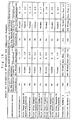
- FIG. 17 is a table showing the results of estimating the
semiconductor devices of the first embodiment and the first
modifications of the first embodiment;
- FIG. 18 is a table showing the results of estimating the
semiconductor devices of the second modifications and the third
modifications with respect to comparison examples;
- FIGS. 19(A), 19(B) and 19(C) are manufacturing step views
of a multilayer printed circuit board according to the second
embodiment of the present invention;
- FIGS. 20(A), 20(B) and 20(C) are manufacturing step views
of the multilayer printed circuit board according to the second
embodiment;
- FIGS. 21(A), 21(B) and 21(C) are manufacturing step views
of the multilayer printed circuit board according to the second
embodiment;
- FIGS. 22(A), 22(B) and 22(C) are manufacturing step views
of the multilayer printed circuit board according to the second
embodiment;
- FIGS. 23(A), 23(B) and 23(C) are manufacturing step views
of the multilayer printed circuit board according to the second
embodiment;
- FIG. 24 is a cross-sectional view of the multilayer printed
circuit board according to the second embodiment;
- FIGS. 25(A), 25(B), 25(C) and 25(D) are manufacturing step
views of a multilayer printed circuit board according to the
first modification of the second embodiment;
- FIG. 26 is a cross-sectional view of the multilayer printed
circuit board according to the first modification of the second
embodiment;
- FIGS. 27(A), 27(B) and 27(C) are manufacturing step views
of a multilayer printed circuit board according to the second
modification of the second embodiment;
- FIGS. 28(A), 28(B) and 28(C) are manufacturing step views
of a multilayer printed circuit board according to the third
embodiment of the present invention;
- FIGS. 29(A), 29(B) and 29(C) are manufacturing step views
of the multilayer printed circuit board according to the third
embodiment;
- FIGS. 30(A), 30(B) and 30(C) are manufacturing step views
of the multilayer printed circuit board according to the third
embodiment;
- FIGS. 31(A), 31(B) and 31(C) are manufacturing step views
of the multilayer printed circuit board according to the third
embodiment;
- FIGS. 32(A), 32(B) and 32(C) are manufacturing step views
of the multilayer printed circuit board according to the third
embodiment;
- FIG. 33 is a cross-sectional view of the multilayer printed
circuit board according to the third embodiment;
- FIGS. 34(A), 34(B), 34(C) and 34(D) are manufacturing step
views of a multilayer printed circuit board according to the
first modification of the third embodiment;
- FIG. 35 is a cross-sectional view of the multilayer printed
circuit board according to the first modification of the third
embodiment;
- FIGS. 36(A), 36(B) and 36(C) are manufacturing step views
of the multilayer printed circuit board according to the first
modification of the third embodiment;
- FIGS. 37(A), 37(B) and 37(C) are manufacturing step views
of the multilayer printed circuit board according to the first
modification of the third embodiment;
- FIGS. 38(A), 38(B) and 38(C) are manufacturing step views
of the multilayer printed circuit board according to the first
modification of the third embodiment;
- FIGS. 39(A), 39(B) and 39(C) are manufacturing step views
of the multilayer printed circuit board according to the first
modification of the third embodiment;
- FIGS. 40(A), 40(B) and 40(C) are manufacturing step views
of the multilayer printed circuit board according to the first
modification of the third embodiment;
- FIG. 41 is a cross-sectional view of the multilayer printed
circuit board according to the first modification of the third
embodiment;
- FIGS. 42(A), 42(B), 42(C) and 42(D) are manufacturing step
views of a multilayer printed circuit board according to the
first other example of the first modification;
- FIG. 43 is a cross-sectional view of a multilayer printed
circuit board according to the first other example of the first
modification;
- FIGS. 44(A), 44(B) and 44(C) are manufacturing step views
of a multilayer printed circuit board according to the second
other example of the first modification of the third embodiment;
- FIGS. 45(A), 45(B), 45(C), 45(D) and 45(E) are
manufacturing step views of a multilayer printed circuit board
according to the second modification of the third embodiment;
- FIGS. 46(A), 46(B), 46(C) and 46(D) are manufacturing step
views of the multilayer printed circuit board according to the
second modification of the third embodiment;
- FIGS. 47(A), 47(B) and 47(C) are manufacturing step views
of the multilayer printed circuit board according to the second
modification of the third embodiment;
- FIGS. 48(A), 48(B) and 48(C) are manufacturing step views
of the multilayer printed circuit board according to the second
modification of the third embodiment;
- FIGS. 49(A), 49(B) and 49(C) are manufacturing step views
of the multilayer printed circuit board according to the second
modification of the third embodiment;
- FIG. 50 is a cross-sectional view of the second
modification of the third embodiment;
- FIGS. 51(A), 51(B), 51(C) and 51(D) are manufacturing step
views of a multilayer printed circuit board according to the
first other example of the second modification of the third
embodiment;
- FIG. 52 is a cross-sectional view of the multilayer printed
circuit board according to the first other example of the second
modification;
- FIGS. 53(A), 53(B), 53(C), 53(D) and 53(E) are
manufacturing step views of a multilayer printed circuit board
according to the fourth embodiment of the present invention;
- FIGS. 54(A), 54(B), 54(C), 54(D) and 54(E) are
manufacturing step views of the multilayer printed circuit board
according to the fourth embodiment;
- FIGS. 55(A), 55(B), 55(C) and 55(D) are manufacturing step
views of the multilayer printed circuit board according to the
fourth embodiment;
- FIGS. 56(A), 56(B) and 56(C) are manufacturing step views
of the multilayer printed circuit board according to the fourth
embodiment;
- FIG. 57 is a cross-sectional view of the multilayer printed
circuit board according to the fourth embodiment;
- FIGS. 58(A), 58(B), 58(C) and 58(D) are manufacturing step
views of a multilayer printed circuit board according to the
fifth embodiment of the present invention;
- FIGS. 59(A), 59(B) and 59(C) are manufacturing step views
of the multilayer printed circuit board according to the fifth
embodiment;
- FIGS. 60(A), 60(B) and 60(C) are manufacturing step views
of the multilayer printed circuit board according to the fifth
embodiment;
- FIGS. 61(A), 61(B) and 61(C) are manufacturing step views
of the multilayer printed circuit board according to the fifth
embodiment;
- FIGS. 62(A) and 62(B) are manufacturing step views of the
multilayer printed circuit board according to the fifth
embodiment;
- FIG. 63 is across-sectional view of the multilayer printed
circuit board according to the fifth embodiment;
- FIG. 64 is a cross-sectional view of the multilayer printed
circuit board according to the fifth embodiment;
- FIG. 65 is a cross-sectional view taken along line E-E
of FIG. 63;
- FIG. 66(A) is a plan view of the multilayer printed circuit
board according to the fifth embodiment, FIG. 66(B) is a plan
view of the multilayer printed circuit board on which bumps are
arranged in a staggered manner and FIG. 66(C) is a plan view
of a multilayer printed circuit board according to a comparison;
- FIGS. 67(A), 67(B) and 67(C) are manufacturing step views
of a multilayer printed circuit board according to another
example of the fifth embodiment;
- FIGS. 68(A), 68(B) and 68(C) are manufacturing step views
of a multilayer printed circuit board according to first
modification of the fifth embodiment of the present invention;
- FIGS. 69(A), 69(B) and 69(C) are manufacturing step views
of the multilayer printed circuit board according to first
modification of the fifth embodiment; and
- FIGS. 70(A), 70(B) and 70(C) are manufacturing step views
of the multilayer printed circuit board according to first
modification of the fifth embodiment.
-
Best Modes for Working the Invention
-
The embodiments of the present invention will be described
hereinafter with reference to the drawings.
A. Semiconductor Device
-
First, the constitution of a semiconductor device (or an
IC chip) according to the first embodiment of the present
invention will be described with reference to FIG. 3(A) which
is a cross-sectional view of a semiconductor device 20 and to
FIG. 4(B) which is a plan view thereof.
[First Embodiment]
-
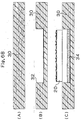
As shown in FIG. 3(B), die pads 22 and wirings (not shown)
are arranged on the upper surface of the semiconductor device
20, a protective film 24 is applied on the respective die pads
22 and wirings and the openings of the protective film 24 are
formed on the respective die pads 22. Transition layers 38 mainly
comprising copper are formed on the respective die pads 22. Each
transition layer 38 comprises a thin film layer 33 and a thickening
layer 37. In other words, the transition layer 38 is formed
out of metallic films of two or more layers.
-
Next, the method of manufacturing the semiconductor device
stated above with reference to FIG. 3(B) will be described with
reference to FIGS. 1 to 4.
- (1) First, wirings 21 and die pads 22 are formed on a silicon
wafer 20A shown in FIG. 1(A) in an established manner (see FIG.
1(B) and FIG. 4(A) which is a plan view of FIG. 1(B), it is noted
that FIG. 1(B) is a cross-sectional view taken along B-B of FIG.
4(A)).
- (2) Next, a protective film 24 is formed on the respective
die pads 22 and wirings 21 and openings 24a are formed on the
respective die pads 22 (see FIG. 1(C)).
- (3) Physical deposition such as deposition or sputtering is
conducted to the silicon wafer 20A, thereby forming a conductive
metallic film (or a thin film layer) 33 on the entire surface
of the silicon wafer 20A (see FIG. 2(A)). It is preferable that
the thickness of the conductive metallic film is in the range
of 0.001 to 2.0 µm. If the thickness is below that range, the
thin film layer cannot be formed on the entire surface. If the
thickness exceeds that range, the thickness of the formed film
becomes irregular. The optimum range is between 0.01 and 1.0
µm. Metal for use in the formation of the metallic film is
preferably selected from a group comprising tin, chromium,
titanium, nickel, zinc, cobalt, gold and copper. The metal
serves as the protective film of the die pads and the electrical
characteristics of the metal does not deteriorate. In the first
embodiment, the thin film layer 33 is formed out of chromium
by sputtering. Chromium is good in adhesiveness to metal and
is capable of suppressing the entry of moisture. It is also
possible to provide copper on the chromium layer by sputtering.
Alternatively, two layers of chromium and copper can be formed
continuously in a vacuum chamber. At this moment, the thickness
of the chromium layer is about 0.05 to 0.1 µm and that of the
copper layer is about 0.5 µm.
- (4) Then, a resist layer made of a liquid resist, a
photosensitive resist or a dry film is formed on the thin film
33. A mask (not shown) on which portions on which transition
films 38 are formed are drawn is put on the resist layer, exposure
and development are conducted and portions 35a on which the resist
35 is not formed are thereby formed. Electroless plating is
conducted to thereby provide thickening layers (or electroplated
films) 37 on the respective resist layer unformed portions 35a
(see FIG. 2(B)). Types of plating materials include copper,
nickel, gold, silver, zinc, iron and the like. In view of
electrical characteristics, inexpensiveness and the fact that
a conductor layer to be built up in a later step mainly comprise
copper, copper is preferable. In the first embodiment, copper
is used. The thickness of each thickening layer 37 is preferably
in the range of 1 to 20 µm.
- (5) After removing the plating resist 35 with an alkaline
solution or the like, the metallic film 33 under the plating
resist 35 is removed with an etching solution of sulfuric
acid-oxygenated water, ferric chloride, cupric chloride, cupric
complex-organic acid salt or the like, thereby forming transition
layers 38 on the respective pads 22 of the IC chip (see FIG.
2(C)).
- (6) Next, an etching solution is sprayed on the substrate and
the surfaces of the transition layers 38 are etched, thereby
forming rough surfaces 38 α (see FIG. 3(A)). The rough surfaces
38α can be formed by conducting electroless plating or an
oxidization-reduction process.
- (7) Finally, the silicon wafer 20A on which the transition
layers 38 are formed are divided into pieces by dicing or the
like and semiconductor devices 20 are formed (see FIGS. 3(B)
and FIG. 4(B) which is a plan view of FIG. 3(B)). Thereafter,
an operation verification test and/or an electrical test may
be conducted to the divided semiconductor devices 20 at need.
Since the transition layers 38 larger than the die pads 22 are
formed on each semiconductor device 20, a probe pin can be easily
contacted with the semiconductor device 20 and test accuracy
is high.
-
[First Other example of First Embodiment]
-
In the above-stated first embodiment, the thin film layer
33 is formed out of chromium. In the first other example, by
contrast, the thin film layer 33 is formed out of titanium.
Titanium is provided by deposition or sputtering. Since
titanium has good adhesiveness to metal, it is possible to
suppress the entry of moisture.
[Second Other Example of First Embodiment]
-
In the above-stated first embodiment, the thin film layer
33 is formed out of chromium. In the second other example, by
contrast, a thin film layer 33 is formed out of tin. Since tin
has good adhesiveness to metal, it is possible to suppress the
entry of moisture.
[Third Other Example of First Embodiment]
-
In the above-stated first embodiment, a thin film layer
33 is formed out of chromium. In the third other example, by
contrast, the thin film layer 33 is formed out of zinc.
[Fourth Other Example of First Embodiment]
-
In the above-stated first embodiment, a thin film layer
33 is formed out of chromium. In the fourth other example, by
contrast, the thin film layer 33 is formed out of nickel. Nickel
is provided by sputtering. Since nickel has good adhesiveness
to metal, it is possible to suppress the entry of moisture.
[Fifth Other Example of First Embodiment]
-
In the above-stated first embodiment, a thin film layer
33 is formed out of chromium. In the fifth other example, by
contrast, the thin film layer 33 is formed out of cobalt.
-
In each of the above other examples, copper may be further
built up on the thin film layer.
[First Modification of First Embodiment]
-
A semiconductor device 20 according to the first
modification of the first embodiment will be described with
reference to FIG. 7(B). In case of the semiconductor device
according to the first embodiment stated above with reference
to FIG. 3(B), each of the transition layers 38 has a two-layer
structure comprising the thin film layer 33 and the thickening
layer 37. In the first modification, by contrast, each
transition layer 38 is constituted to have a three-layer
structure comprising the first thin film layer 33, the second
thin film layer 36 and a thickening layer 37 as shown in FIG.
7(B).
-
Next, the method of manufacturing the semiconductor device
according to the first modification described above with
reference to FIG. 7(B) will be described with reference to FIGS.
5 to 7.
- (1) First, wirings 21 and die pads 22 are formed on a silicon
wafer 20A shown in FIG. 5(A) (see FIG. 5(B)).
- (2) Next, a protective film 24 is formed on the wirings 21
and the die pads 22 (see FIG. 5(C)).
- (3) Physical deposition such as deposition or sputtering is
conducted to the silicon wafer 20A, thereby forming a conductive
metallic film (or the first thin film layer) 33 on the entire
surface of the silicon wafer 20A (see FIG. 5(D)). The thickness
of the metallic film is preferably in the range of 0.001 to 2.0
µm. If the thickness is below that range, the thin film layer
cannot be formed. If the thickness exceeds that range, the
thickness of the formed film becomes irregular. The optimum
range is between 0.01 to 1.0µm. Metal for use in the formation
of the metallic film is preferably selected from a group
comprising tin, chromium, titanium, nickel, zinc, cobalt, gold
and copper. The metal serves as the protective film of the die
pads and the electrical characteristics of the metal does not
deteriorate. Since chromium, nickel and titanium have good
adhesiveness to metal, they can suppress the entry of moisture.
In the first modification, the first thin film layer 33 is formed
out of chromium.
- (4) The second thin film layer 36 is built up on the first
thin film layer 33 by any one of sputtering, deposition and
electroless plating methods(see FIG. 6(A)). Metal to be built
up is preferably selected from a group comprising nickel, copper,
gold and silver. It is more preferable to form the second thin
film layer 36 out of copper or nickel. The reason is as follows.
Copper is inexpensive and good in electrical conductivity.
Nickel is good in adhesiveness to a thin film and hardly peeled
or cracked. The thickness of the second thin film layer 36 is
preferably 0.01 to 5.0 µm and more preferably 0.1 to 3.0 µm.
In the first modification, the second thin film layer 36 is formed
by electroless copper plating.
The preferable combinations of the first and second thin
film layers are chromium-copper layers, chromium-nickel layers,
titanium-copper layers, titanium-nickel layers and the like.
These combinations are superior to the other combinations in
coupling characteristics with respect to metal and electrical
conductivity.
- (5) Thereafter, a resist layer is formed on the second thin
film layer 36. A mask (not shown) is put on the resist layer,
exposure and development are conducted and portions 35a on which
the resist 35 is not formed are formed. Thickening layers (or
electroless plated layers) 37 are provided on the resist unformed
sections 35a by electroplating (see FIG. 6(B)). Types of plating
materials used in the formation of plated layers include copper,
nickel, gold, silver, zinc, iron and the like. In view of
electrical characteristics, inexpensiveness and the fact that
a conductor layer to be built up in a later step mainly comprises
copper, copper is preferable. In the first modification.
therefore, copper is used. The thickness of each thickening
layer 37 is preferably in the range of 1 to 20µm.
- (6) After removing the plating resist 35 with an alkaline
solution or the like, the second thin film layer 36 and the metallic
film 33 under the plating resist 35 are removed with an etching
solution of sulfuric acid-oxygenated water, ferric chloride,
cupric chloride, cupric complex-organic acid salt or the like,
thereby forming transition layers 38 on the respective pads 22
of the IC chip (see FIG. 6(C)).
- (7) Next, an etching solution is sprayed on the substrate and
the surfaces of the transition layers 38 are etched, thereby
forming rough surfaces 38a (see FIG. 7(A)). The rough surfaces
38a can be formed by conducting electroless plating or an
oxidization-reduction process.
- (8) Finally, the silicon wafer 20A on which the transition
layers 38 are formed are divided into pieces by dicing or the
like and semiconductor devices are formed (see FIG. 7(B)).
-
[First Other Example of First Modification of First Embodiment]
-
In the first modification stated above, the first thin
layer 33 is formed out of chromium, the second thin film layer
36 is formed by electroless copper plating and the thickening
layer 37 is formed by copper electroplating. In the first other
example, by contrast, the first thin film layer 33 is formed
out of chromium, the second thin film layer 36 is formed by
sputtering copper and the thickening layer 37 is formed by copper
electroplating. The thickness of the chromium layer is 0.07µm,
that of the copper layer is 0.5µm and that of the electroplated
copper layer is 15 µm.
[Second Other Example of First Modification of First Embodiment]
-
In the second other example, the first thin film layer
33 is formed out of titanium, the second thin film layer 36 is
formed by electroless copper plating and the thickening layer
37 is formed by copper electroplating. The thickness of the
titanium layer is 0.07 µm, that of the copper plated layer is
1.0µm and that of the copper electroplated layer is 17µm.
[Third Other Example of First Modification of First Embodiment]
-
In the third other example, the first thin film layer 33
is formed out of titanium, the second thin film layer 36 is formed
by sputtering copper and the thickening layer 37 is formed by
copper electroplating. The thickness of the titanium layer is
0.06 µm, that of the copper layer is 0.5 µm and that of the copper
electroplated layer is 15 µm.
[Fourth Other Example of First Modification of First Embodiment]
-
In.the fourth other example, the first thin film layer
33 is formed out of chromium, the second thin film layer 36 is
formed by electroless nickel plating and the thickening layer
37 is formed by copper electroplating. The thickness of the
chromium layer is 0.07 µm, that of the copper plated layer is
1.0 µm and the copper electroplated layer is 15 µm.
[Fifth Other Example of First Modification of First Embodiment]
-
In the fifth example, the thin film layer 33 is formed
out of titanium, the second thin film layer 36 is formed by
electroless nickel plating and the thickening layer 37 is formed
by copper electroplating. The thickness of the titanium layer
is 0.05 µm, that of the nickel plated layer is 1.2 µm and that
of the copper electroplated layer is 15 µm.
[Second Modification of First Embodiment]
-
The method of manufacturing a semiconductor device 20
according to the second modification will be described with
reference to FIG. 8. The constitution of the semiconductor
device in the second modification is almost the same as that
in the first embodiment stated above with reference to FIG. 3(B).
In the first embodiment, a semi-additive step is employed and
the thickening layers 37 are formed on the respective resist
unformed portions, thereby forming the transition layers 38.
In the second modification, by contrast, an additive step is
employed and thickening layers 37 are uniformly formed.
Thereafter, a resist is provided and resist unformed portions
are etched away, thereby forming transition layers 38.
-
The manufacturing method in the second modification will
be described with reference to FIG. 8.
- (1) As described above in the first embodiment with reference
to FIG. 2(B), physical deposition such as deposition or
sputtering is conducted to a silicon wafer 20A, thereby forming
a conductive metallic film 33 on the entire surface of the silicon
wafer 20A (see FIG. 8(A)). The thickness of the conductive
metallic film 33 is preferably in the range of 0.001 to 2.0 µm.
If the thickness is below that range, a thin film layer cannot
be formed on the entire surface. If the thickness exceeds that
range, the thickness of the film to be formed becomes irregular.
The optimum range is preferably 0.01 to 1.0 µm. Metal for use
in the formation of the metallic film 33 is preferably selected
from a group comprising tin, chromium, titanium, nickel, zinc,
cobalt, gold and copper. The metal serves as the protective
film of die pads and the electrical characteristics of the metal
does not deteriorate. In the second modification, the thin film
layer 33 is formed by sputtering chromium. The thickness of
the chromium thin film layer 33 is 0.05 µm.
- (2) Electroplating is conducted to provide a thickening layer
(or an electroplated film) 37 on the thin film layer 33 (see
FIG. 8(B)). Types of plating materials include copper, nickel,
gold, silver, zinc, iron and the like. In view of electrical
characteristics, inexpensiveness and the fact that a conductor
layer to be built up in a later step mainly comprises copper,
copper is preferable. In the second modification, therefore,
copper is used. The thickness of the thickening layer 37 is
preferably in the range of 1.0 to 20 µm. If the thickness exceeds
that range, undercut may possibly occur during etching to be
described later to thereby generate gaps in the interfaces
between a transition layer and via holes to be formed.
- (3) Thereafter, a resist layer 35 is formed on the thickening
layer 37 (see FIG. 8(C)).
- (4) The metallic film 33 and the thickening layer 37 on the
portions on which the resist 35 is not formed are etched away
with an etching solution of sulfuric acid-oxygenated water,
ferric chloride, cupric chloride, cupric complex-organic acid
salt or the like, thereby forming transition layers 38 on the
respective pads 22 of the IC chip (see FIG. 8(D)). Since
following steps are the same as those in-the first embodiment,
no description will be given thereto.
-
[First Other Example of Second Modification of First Embodiment]
-
In the second modification stated above, the thin film
layer 33 is formed out of chromium. In the first other example,
by contrast, a thin film layer 33 is formed out of titanium.
[Third Modification of First Embodiment]
-
The method of manufacturing a semiconductor device 20
according to the third modification will be described with
reference to FIG. 9. In case of the semiconductor device
according to the second modification stated above with reference
to FIG. 8, each transition layer 38 has a two-layer structure
comprising the thin film layer 33 and the thickening layer 37.
In the third modification, as shown Fig. 9 (D), by contrast,
a transition layer 38 is constituted to have a three-layer
structure comprising the first thin film layer 33, the second
thin film layer 36 and a thickening layer 37.
-
The manufacturing method in the third modification will
be described with reference to FIG. 9.
- (1) As in the case of the first modification in the first
embodiment stated above with reference to FIG. 6(A), the second
thin film layer 36 is built up on the first thin film layer 33
by sputtering, deposition or electroless plating (see FIG. 9(A)).
Metal to be built up in this case is preferably selected from
a group comprising nickel, copper, gold and silver. Copper or
nickel is more preferable. The reason is as follows. Copper
is inexpensive and good in electrical conductivity. Nickel is
good in adhesiveness to a thin film and is hardly peeled or cracked.
In the third modification, the second thin film layer 36 is formed
by electroless copper plating. The thickness of the second thin
film layer 36 is preferably 0.01 to 5.0 µm and more preferably
0.1 to 3.0 µm.
The preferable combinations of the first thin film layer
and the second thin film layer are chromium-copper layers,
chromium-nickel layers, titanium-copper layers,
titanium-nickel layers. These combinations are superior to the
other combinations in coupling characteristics with respect to
metal and electrical conductivity.
- (2) Electroplating is conducted, thereby uniformly providing
a thickening layer 37 made of nickel, copper, gold, silver, zinc
or iron on the second thin film layer 36 (see FIG. 9(B)). The
thickness of the thickening layer 37 is preferably 1 to 20 µm.
- (3) Thereafter, a resist layer 35 is formed on the thickening
layer 37 (see FIG. 9(C)).
- (4) The first thin film layer 33, the second thin film layer
36 and the thickening layer 37 on portions on which the resist
35 is not formed are removed with an etching solution of sulfuric
acid-oxygenated water, ferric chloride, cupric chloride, cupric
complex-organic acid salt or the like and the resist 35 is peeled,
thereby forming transition layers 38 on the respective pads 22
of the IC chip (see FIG. 9(D)). Since following steps are the
same as those in the first embodiment, no description will be
given thereto.
-
[First Other Example of Third Modification of First Embodiment]
-
In the third modification stated above, the first thin
film layer 33 is formed out of chromium, the second thin film
layer 36 is formed by electroless copper plating and the
thickening layer 37 is formed by copper electroplating. In the
first other example, by contrast, the first thin film layer 33
is formed out of chromium, the second thin film layer 36 is formed
by sputtering copper and a thickening layer 37 is formed by-copper
electroplating. The thickness of the chromium layer is 0.07
µm, that of the copper layer is 0.5 µm and that of the copper
electroplated layer is 15 µm.
[ Second Other Example of Third Modification of First Embodiment]
-
In the second other example, the first thin film layer
33 is formed out of titanium, the second thin film layer 36 is
formed by electroless copper plating and a thickening layer 37
is formed by copper electroplating. The thickness of the
titanium layer is 0.07 µm, that of the copper layer is 1.0 µm
and that of the copper electroplated layer is 15 µm.
[Third Other Example of Third Modification of First Embodiment]
-
In the third other example, the first thin film layer 33
is formed out of titanium, the second thin film layer 36 is formed
by sputtering copper and the thickening layer 37 is formed by
copper electroplating. The thickness of the titanium layer is
0.07 µm, that of the copper layer is 0.5 µm and that of the copper
electroplated layer is 18 µm.
[Fourth Other Example of Third Modification of First Embodiment]
-
In the fourth other example, the first thin film layer
33 is formed out of chromium, the second thin film layer 36 is
formed by electroless nickel plating and a thickening layer 37
is formed by copper electroplating. The thickness of the
chromium layer is 0.06 µm, that of the nickel layer is 1.2 µm
and that of the copper electroplated layer is 16 µm.
[ Fifth Other Example of Third Modification of First Embodiment]
-
In the fifth other example, the first thin film layer 33
is formed out of titanium, the second thin film layer 36 is formed
by electroless nickel plating and a thickening layer 37 is formed
by copper electroplating. The thickness of the titanium layer
is 0.07 µm, that of the nickel layer is 1.1 µm and that of the
copper electroplated layer is 15 µm.
B. Multilayer Printed Circuit Board into which Semiconductor
Device is Integrated.
-
Next, description will be given to the constitution of
a multilayer printed circuit board provided by embedding and
containing a semiconductor device (or an IC chip) 20 in the
above-stated first to third modifications into the recess, gap
or opening of a core substrate.
[First Embodiment]
-
As shown in FIG. 14, the multilayer printed circuit board
10 comprises a core substrate 30 containing therein an IC chip
20, an interlayer resin insulating layer 50 and an interlayer
resin insulating layer 150. Via holes 60 and conductor circuits
58 are formed on the interlayer resin insulating layer 50. Via
holes 160 and conductor circuits 158 are formed on the interlayer
resin insulating layer 150.
-
A solder resist layer 70 is provided on the interlayer
resin insulating layer 150. Solder bumps 76 for connecting to
an external substrate such as a daughter board or a mother board,
which is not shown in FIG. 14, are provided on the conductor
circuits 158 under the openings 71 of the solder resist layer
70, respectively.
-
In the multilayer printed circuit board 10 in this
embodiment, the IC chip 20 is integrated into the core substrate
30 and transition layers 38 are provided on the respective pads
22 of the IC chip 20. Due to this, it is possible to electrically
connect the IC chip to the multilayer printed circuit board (or
package substrate) without using lead members and a sealing resin.
Further, since the transition layers 38 are formed on the IC
chip portion, the IC chip portion is flattened and the upper
interlayer insulating layer 50 is, therefore, flattened to
thereby provide uniform film thickness. Further, because of
the transition layers, it is possible to maintain the stability
of shape even if the via holes 60 provided in the upper layer
are formed.
-
Furthermore, by providing the transition layers 38 made
of copper on the respective die pads 22, it is possible to prevent
resin residues on the die pads 22 and to prevent the die pads
22 from being discolored or dissolved even after impregnating
the multilayer printed circuit board in an acid, an oxidizer
or an etching solution in a later step or conducting various
annealing steps. Thus, connection characteristic between the
die pads of the IC chip and the via holes and reliability can
be improved. Besides, by interposing the transition layers 38
each having a diameter of 60µm or more on the respective pads
22 each having a diameter of 40 µm, it is possible to ensure
connecting the via holes each having a diameter of 60 µm.
-
Next, the method of manufacturing the multilayer printed
circuit board described above with reference to FIG. 14 will
be described with reference to FIGS. 10 to 13.
- (1) First, an insulating resin substrate (or a core substrate)
30 in which prepregs each having a core material made of glass
cloths or the like and impregnated with a resin such as epoxy
are built up, is used as a starting material (see FIG. 10(A)).
Next, a recess 32 for containing an IC chip is formed on one
side of the core substrate 30 by counter boring (see FIG. 10(B).
While the recess is provided by counter boring herein, it is
also possible to form a core substrate having a containing section
by building up an insulating resin substrate having an opening
to an insulating resin substrate without an opening.
- (2) Then, an adhesive material 34 is applied to the recess
32 using a printing machine. At this time, potting instead of
application may be conducted. Next, an IC chip 20 is mounted
on the adhesive material 34 (see FIG. 10(C)).
- (3) Then, the upper surface of the IC chip 20 is depressed
or struck to thereby completely contain the IC chip 20 in the
recess 32 (see FIG. 10(D). By doing so, the core substrate 30
can be smoothed. At this moment, the adhesive material 34 is
sometimes applied on the upper surface of the IC chip 20. However,
as described later, since a resin layer is provided on the upper
surface of the IC chip 20 and then openings for via holes are
provided by laser, the adhesive material 34 does not influence
the connection between transition layers 38 and via holes.
- (4) A thermosetting resin sheet having a thickness of 50 µm
is vacuum-compression laminated onto the substrate which has
gone through the above-stated steps at a pressure of 5 kg/cm2
while raising temperature to 50 to 150° C, thereby providing an
interlayer resin insulating layer 50 (see FIG. 11(A)). The
degree of vacuum at the time of vacuum compression is 10 mmHg.
- (5) Next, using CO2 gas laser having a wavelength of 10.4 µm,
via hole openings 48 each having a diameter of 60 µm are provided
in the interlayer resin insulating layer 50 under the conditions
of a beam diameter of 5 mm, a top hat mode, a pulse width of
5.0 microseconds, a mask hole diameter of 0.5 mm and one shot
(see FIG. 11(B)). Using a permanganic acid at a temperature
of 60° C, resin residues in the openings 48 are removed. By
providing a transition layer 38 made of copper on each die pad
22, it is possible to prevent resin residues on the pad 22, thereby
improving connection characteristic between the pad 22 and a
via hole 60 to be described later and improving reliability.
Furthermore, by interposing the transition layer 38 having a
diameter of 60 µm or more on the die pad 22 having a diameter
of 40 µm, it is possible to ensure connecting the via hole opening
48 having a diameter of 60 µm. While the resin residues are
removed by using an oxidizer such as apermanganic acid, a de-smear
process can be also conducted using oxygen plasma or corona
process.
- (6) Next, the resultant substrate is immersed in an oxidizer
such as a chromic acid or a permanganic acid or the like, thereby
providing a rough surface 50α on the interlayer resin insulating
layer 50 (see FIG. 11(c)). The rough surface 50α is preferably
formed to have a thickness in the range of 0.1 to 5 µm. For
example, the substrate is immersed in 50 g/l of a sodium
permanganate solution at a temperature of 60° C for 5 to 25 minutes,
thereby providing a rough surface 50 α of 2 to 3 µm.
Alternatively, by performing a plasma process using SV-4540
manufactured by ULVAC JAPAN LTD., the rough surface 50α can
be formed on the surface of interlayer resin insulating layer
50. In that case, argon gas is used as inactive gas to perform
a plasma process for two minutes under conditions of electric
power of 200W, a gas pressure of 0.6 Pa and a temperature of
70°C.
- (7) A metallic layer 52 is provided on the interlayer resin
insulating layer 50 on which the rough surface 50α has been
formed (see FIG. 12(A)). The metallic layer 52 is formed by
electroless plating. By supplying a catalyst such as a palladium
catalyst to the surface layer of the interlayer resin insulating
layer 50 in advance and immersing the substrate into an
electroless plating solution for 5 to 60 minutes, the metallic
layer 52 which is a plated film is provided in the range of 0.1
to 5 µm. For example, the substrate is immersed in the following
solution at a solution temperature of 34°C for 40 minutes:
-
[Electroless Plating Solution]
-
| NiSO4 |
0.003 mol/l |
| tartaric acid |
0.200 mol/l |
| copper sulfate |
0.030 mol/l |
| HCHO |
0.050 mol/l |
| NaOH |
0.100 mol/l |
| α, α'-bipyridyl |
100 mg/l |
| polyethylene glycol (PEG) |
0.10 g/l |
-
Alternatively, an Ni/
Cu alloy 52 can be formed on the
surface of the interlayer epoxy
resin insulating layer 50 by
conducting sputtering with an Ni-
Cu alloy 52 as a target under
conditions of an air pressure of 0.6 Pa, a temperature of 80° C,
power of 200W and a duration of five minutes using SV-4540
manufactured by ULVAC JAPAN LTD.. At this moment, the thickness
of the Ni-
Cu alloy layer 52 thus formed is 0.2 µm.
- (8) A commercially available photosensitive dry film is bonded
to the substrate 30 which has been subjected to the above process,
a photomask film is mounted, exposure is conducted at 100 mj/cm2
and then a development process is conducted with 0.8% sodium
carbonate, thereby providing a plating resist 54 having a
thickness of 15 µm. Next, electroplating is conducted under the
following conditions, thereby forming an electroplated firm (see
FIG. 12(B)). An additive in the electroplating solution is
Kapalacid HL manufactured by Atotech Japan.
-
[Electroplating Solution]
-
| sulfuric acid |
2.24 mol/l |
| copper sulfate |
0.26 mol/l |
| additive |
19.5 mol/l |
| (Kapalacid HL manufactured by Atotech Japan) |
[Electroplating Conditions]
-
| current density |
1 A/dm2 |
| duration |
65 minutes |
| temperature |
| |
22±2° C |
- (9) After separating and removing the plating resist with
5%NaOH, the metallic layer 52 under the plating resist is
dissolved and removed by etching using a mixture solution of
a nitric acid, a sulfuric acid and oxygenated water, conductor
circuits 58 each comprising the metallic layer 52 and the
electroplated film 56 and having a thickness of 16 µm and via
holes 60 are formed and etched by an etching solution containing
a cupric salt complex and an organic acid, thereby forming rough
surfaces 58α and 60α (see FIG. 12(C)).
- (10) Next, the steps of (4) to (9) stated above are repeated,
thereby forming an upper interlayer resin insulating layer 150
and conductor circuits 158 (including via holes 160) (see FIG.
13(A)).
- (11) Then, 46.67 parts by weight of oligomer (having amolecular
weight of 4000) which is obtained by forming 50% of epoxy groups
of 60 parts by weight of a cresol novolac epoxy resin (manufactured
by Nippon Kayaku Co., Ltd.) dissolved in diethylene glycol
dimethyl ether (DMDG) into an acrylic structure and which imparts
photosensitive characteristic, 15 parts by weight of 80 wt% of
a bisphenol A epoxy resin (product name: Epicoat 1001
manufactured by Yuka Shell) dissolved in methylethyl keton, 1.6
parts by weight of an imidazole hardening agent (product name:
2E4MZ-CN manufactured by Shikoku Chemicals Corp.), 3 parts by
weight of polyhydric acryl monomer which is a photosensitive
monomer (product name: R604 manufactured by Kyoei Chemical),
1.5 parts by weight of polyhydric acryl monomer (product name:
DPE6A manufactured by Kyoei Chemical), and 0.71 parts by weight
of a dispersing defoaming agent (product name: S-65 manufactured
by Sannopuko) are contained in a container, agitated and mixed
to adjust mixture compositions. Then, 2.0 parts by weight of
benzophenone (manufactured by Kanto Chemical) serving as a
photoinitiator and 0.2 parts by weight of Michler's ketone
(manufactured by Kanto Chemical) serving as a photosensitizer
are added to the mixture compositions, thereby obtaining a solder
resist composition (or organic resin insulating material)
adjusted to have a viscosity of 2.0 Pa·s.
It is noted that the viscosity is measured by using No.
4 rotor of a B-type viscometer (DVL-B manufactured by Tokyo Keiki)
when the velocity is 60 rpm and using No. 3 rotor of the same
when the velocity is 6 rpm.
- (12) Next, the solder resist composition is applied to the
substrate 30 to have a thickness of 20 µm and a drying process
is conducted at 70°C for 20 minutes and 70°C for 30 minutes.
Then, a photomask film having a pattern of the solder resist
opening portions drawn thereon and a thickness of 5 mm is made
hermetic contact with the solder resist layer 70, exposure is
performed with ultraviolet rays with 1000 mj/cm2 and then a
development process is performed with a DMTG solution, thereby
forming openings 71 each having a diameter of 200 µm (see FIG.
13(B)). Alternatively, a commercially available solder resist
may be used.
- (13) Next, the substrate on which the solder resist layer (or
organic resin insulating layer) 70 is formed, is immersed in
an electroless nickel plating solution containing nickel
chloride (2.3 × 10⁻¹ mol/l), sodium hypophosphite (2.8 × 10⁻¹
mol/l), sodium citrate (1.6 × 10⁻¹ mol/l) and having pH = 4.5
for 20 minutes, and a nickel plated layer 72 having a thickness
of 5 µm is formed on each opening portion 71. Then, the substrate
is further immersed in an electroless plating solution containing
gold potassium cyanide (7.6 × 10⁻³ mol/l), ammonia chloride (1.9
× 10-1 mol/l), sodium citrate (1.2 × 10⁻¹ mol/l) and sodium
hypophosphite (1.7 × 10⁻¹ mol/l) under the condition of 80°C
for 7.5 minutes and a gold plated layer 74 having a thickness
of 0.03 µm is formed on the nickel plated layer 72, thereby forming
a solder pad 75 on each conductor layer 158 (see FIG. 13(C)).
- (14) Thereafter, a solder paste is printed on the opening
portions 71 of the solder resist layer 71 and reflow is conducted
at 200° C, thereby forming solder bumps 76. As a result, it is
possible to obtain a multilayer printed circuit board 10 into
which the IC chip 20 is integrated and which has the solder bumps
76 (see FIG. 14).
-
-
As the solder paste, Sn/Pb, Sn/Sb, Sn/Ag, Sn/Ag/Cu or the
like may be used. Needless to say, a solder paste of low a
radiation ray type may be used.
-
In the above-stated embodiment, the thermosetting resin
sheet is used for the interlayer resin insulating layers 50 and
150. The thermosetting resin insulating sheet contains a
refractory resin, soluble particles, a hardening agent and other
components. The materials will now be described one by one.
-
The resin used in the manufacturing method of the present
invention has a structure in that particles soluble in acid or
an oxidizer (hereinafter, referred to as "soluble particles")
are dispersed in resin which is refractory with respect to acid
or an oxidizer (hereinafter, referred to as "refractory resin").
-
The expressions "refractory" and "soluble" will now be
described. When materials are immersed in solution composed
of the same acid or the same oxidizers for the same time, a material
of a type which is dissolved at a relatively high dissolving
rate is called a "soluble" material for convenience. A material
of a type which is dissolved at a relatively slow dissolving
rate is called a "refractory material" for convenience.
-
The soluble particles are exemplified by resin particles
which are soluble in acid or an oxidizer (hereinafter called
"soluble resin particles"), inorganic particles which are
soluble in acid or an oxidizer (hereinafter called "inorganic
soluble particles") and metal particles which are soluble in
acid or an oxidizer (hereinafter called "soluble metal
particles"). The foregoing soluble particles may be employed
solely or two or more particles may be employed.
-
The shape of each of the soluble particles is not limited.
The shape may be a spherical shape or a pulverized shape. It
is preferable that the particles have a uniform shape. The reason
for this lies in that a rough surface having uniformly rough
pits and projections can be formed.
-
It is preferable that the mean particle size of the soluble
particles is 0.1µm to 10µm. When the particles have the
diameters satisfying the foregoing range, particles having two
or more particle sizes may be employed. That is, soluble
particles having a mean particle size of 0.1 µm to 0.5 µm and
soluble particles having a mean particle size of 1 µm to 3
µmm may be mixed. Thus, a more complicated rough surface can
be formed. Moreover, the adhesiveness with the conductor
circuit can be improved. In the present invention, the particle
size of the soluble particles is the length of a longest portion
of each of the soluble particles.
-
The soluble resin particles may be particles constituted
by thermosetting resin or thermoplastic resin. When the
particles are immersed in solution composed of acid or an oxidizer,
the particles must exhibit dissolving rate higher than that of
the foregoing refractory resin.
-
Specifically, the soluble resin particles are exemplified
by particles constituted by epoxy resin, phenol resin, polyimide
resin, polyphenylene resin, polyolefin resin polietelslufon or
fluorine resin. The foregoing material may be employed solely
or two or more materials may be mixed.
-
The soluble resin particles may be resin particles
constituted by rubber. Rubber above is exemplified by
polybutadiene rubber, a variety of denatured polybutadiene
rubber, such as denatured epoxy rubber, denatured urethane rubber
or denatured (metha) acrylonitrile rubber, and (metha)
acrylonitrile butadiene rubber containing a carboxylic group.
When the foregoing rubber material is employed, the soluble resin
particles can easily be dissolved in acid or an oxidizer. That
is, when the soluble resin particles are dissolved with acid,
dissolution is permitted with acid except for strong acid. When
the soluble resin particles are dissolved, dissolution is
permitted with permanganate which has a relatively weak oxidizing
power. When chromic acid is employed, dissolution is permitted
even at a low concentration. Therefore, retention of the acid
or the oxidizer on the surface of the resin can be prevented.
When a catalyst, such as palladium chloride, is supplied after
the rough surface has been formed as described later, inhibition
of supply of the catalyst and oxidation of the catalyst can be
prevented.
-
The inorganic soluble particles are exemplified by
particles made of at least a material selected from a group
comprising an aluminum compound, a calcium compound, a potassium
compound, a magnesium compound and a silicon compound.
-
The aluminum compound is exemplified by alumina and
aluminum hydroxide. The calcium compound is exemplified by
calcium carbonate and calcium hydroxide. The potassium
compound is exemplified by potassium carbonate. The magnesium
compound is exemplified by magnesia, dolomite and basic magnesium
carbonated. The silicon compound is exemplified by silica and
zeolite. The foregoing material may be employed solely or two
or more materials may be mixed.
-
The soluble metal particles are exemplified by particles
constituted by at least one material selected from a group
comprising copper, nickel, iron, zinc, lead, gold, silver,
aluminum, magnesium, potassium and silicon. The soluble metal
particles may have surfaces coated with resin or the like in
order to maintain an insulating characteristic.
-
When two or more types of the soluble particles are mixed,
it is preferable that the combination of the two types of soluble
particles is combination of resin particles and inorganic
particles. Since each of the particles has low conductivity,
an insulating characteristic with the resin film can be
maintained. Moreover, the thermal expansion can easily be
adjusted with the refractory resin. Thus, occurrence of a crack
of the interlayer resin insulating layer constituted by the resin
film can be prevented. Thus, separation between the interlayer
resin insulating layer and the conductor circuit can be
prevented.
-
The refractory resin is not limited when the resin is able
to maintain the shape of the rough surface when the rough surface
is formed on the interlayer resin insulating layer by using acid
or oxidizer. The refractory resin is exemplified by
thermosetting resin, thermoplastic resin and their composite
material. As an alternative to this, the foregoing
photosensitive resin of a type having photosensitive
characteristic imparted thereto may be employed. When the
photosensitive resin is employed, exposure and development
processes of the interlayer resin insulating layers can be
performed to form the openings for the via holes.
-
In particular, it is preferable that the resin containing
thermosetting resin is employed. In the foregoing case, the
shape of the rough surface can be maintained against plating
solution and when a variety of heating processes are performed.
-
The refractory resin is exemplified by epoxy resin, phenol
resin, phenoxy resin, polyimide resin, polyphenylene resin,
polyolefin resin, polyetelslufon and fluorine resin. The
foregoing material may be employed solely or two or more types
of the materials may be mixed.
-
It is preferable that epoxy resin having two or more epoxy
groups in one molecule thereof is employed. The reason for this
lies in that the foregoing rough surface can be formed. Moreover,
excellent heat resistance and the like can be obtained. Thus,
concentration of stress onto the metal layer can be prevented
even under a heat cycle condition. Thus, occurrence of
separation of the metal layer can be prevented.
-
The epoxy resin is exemplified by cresol novolac epoxy
resin, bisphenol-A epoxy resin, bisphenol-F epoxy resin, phenol
novolac epoxy resin, alkylphenol novolac epoxy resin, biphenol-F
epoxy resin, naphthalene epoxy resin, dicyclopentadiene epoxy
resin, an epoxy material constituted by a condensation material
of phenol and an aromatic aldehyde having a phenol hydroxyl group,
triglycidyl isocyanurate and alicyclic epoxy resin. The
foregoing material may be employed solely or two or more material
may be mixed. Thus, excellent heat resistance can be realized.
-
It is preferable that the soluble particles in the resin
film according to the present invention are substantially
uniformly dispersed in the refractory resin. The reason for
this lies in that a rough surface having uniform pits and
projections can be formed. When via holes and through holes
are formed in the resin film, adhesiveness with the metal layer
of the conductor circuit can be maintained. As an alternative
to this, a resin film containing soluble particles in only the
surface on which the rough surface is formed may be employed.
Thus, the portions of the resin film except for the surface is
not exposed to acid or the oxidizer. Therefore, the insulating
characteristic between conductor circuits through the
interlayer resin insulating layer can reliably be maintained.
-
It is preferable that the amount of the soluble particles
which are dispersed in the refractory resin is 3 wt% to 40 wt%
with respect to the resin film. When the amount of mixture of
the soluble particles is lower than 3 wt%, the rough surface
having required pits and projections cannot be formed. When
the amount is higher than 40 wt%, deep portions of the resin
film are undesirably dissolved when the soluble particles are
dissolved by using acid or the oxidizer. Thus, the insulating
characteristic between the conductor circuits through the
interlayer resin insulating layer constituted by the resin film
cannot be maintained. Thus, short circuit is sometimes is caused
to occur.
-
It is preferable that the resin film contains a hardening
agent and other components as well as the refractory resin.
-
The hardening agent is exemplified by an imidazole
hardening agent, an amine hardening agent, a guanidine hardening
agent, an epoxy adduct of each of the foregoing hardening agents,
a microcapsule of each of the foregoing hardening agents and
an organic phosphine compound, such as triphenylphosphine or
tetraphenyl phosphonium tetraphenyl borate.
-
It is preferable that the content of the hardening agent
is 0.05 wt% to 10 wt% with respect to the resin film. When the
content is lower than 0.05 wt%. the resin film cannot sufficiently
be hardened. Thus, introduction of acid and the oxidizer into
the resin film occurs greatly. In the foregoing case, the
insulating characteristic of the resin film sometimes
deteriorates. When the content is higher than 10 wt%, an
excessively large quantity of the hardening agent component
sometimes denatures the composition of the resin. In the
foregoing case, the reliability sometimes deteriorates.
-
The other components are exemplified by an inorganic
compound which does not exert an influence on the formation of
the rough surface and a filler constituted by resin. The
inorganic compound is exemplified by silica, alumina and dolomite.
The resin is exemplified by polyimide resin, polyacrylic resin,
polyamideimide resin, polyphenylene resin, melanine resin and
olefin resin. When anyone of the foregoing fillers is contained,
conformity of the thermal expansion coefficients can be
established. Moreover, heat resistance and chemical resistance
can be improved. As a result, the performance of the multilayer
printed circuit board can be improved.
-
The resin film may contain solvent. The solvent is
exemplified by ketone, such as acetone, methylethylketone or
cyclohexane; aromatic hydrocarbon, such as ethyl acetate, butyl
acetate, cellosolve acetate, toluene or xylene. The foregoing
material may be employed solely or two or more materials may
be mixed. It is noted, however, interlayer resin insulating
layer is resolved and carbonated if heated at a temperature of
350° C or higher.
[First Modification of First Embodiment]
-
Next, description will be given to a multilayer printed
circuit board according to the first modification of the first
embodiment with reference to FIG. 16.
-
In the first embodiment stated above, description has been
given to a case where the BGA's are arranged. In the first
modification, which is almost the same as the first embodiment,
the multilayer printed circuit board is constituted in a PGA
type for establishing connection through conductive connection
pins 96 as shown in FIG. 16. Also, via holes are formed by laser
in the above-stated first embodiment, whereas via holes are
formed by phptoetching in the first modification.
-
The method of manufacturing the multilayer printed circuit
board according to the first modification will be described with
reference to FIG. 15.
- (4) As in the case of the first embodiment, a thermosetting
epoxy resin 50 having a thickness of 50 µm is applied to the
substrate which has gone through the steps (1) to (3) (see FIG.
15(A)).
- (5) Next, a photomask film 49 having black circles 49a
corresponding to via hole formed positions drawn thereon is put
on the interlayer resin insulating layer 50 and exposure is
conducted (see FIG. 15(B)).
- (6) Development is conducted by spraying a DMTG solution and
a heat process is conducted, thereby providing an interlayer
resin insulating layer 50 having openings 48 each having a
diameter of 85 µm for via holes (see FIG. 15(C)).
- (7) The surface of the interlayer resin insulating layer 50
is roughened with a permanganic acid or a chromic acid, thereby
forming a rough surface 50α (see FIG. 15(D)). Since following
steps are the same as those in the first embodiment stated above,
no description will be given thereto. The thickness of the rough
surface 50α is preferably in the range of 0.05 to 5 µm.
-
-
The results of estimating the semiconductor devices in
the above-stated embodiment and semiconductor devices in
comparison examples while containing the devices in the
multilayer printed circuit boards in the first embodiment and
the first modification are shown in tables of FIGS. 17 and 18.
[Comparison Example 1]
-
In comparison example 1, a semiconductor device is the
same as that in the first embodiment. However, in the comparison
example 1, no transition layers are formed and die pads are
directly embedded into a multilayer printed circuit board.
[Comparison Example 2]
-
In comparison example 2, stud bumps described in Japanese
Patent Laid-Open No. 9-321408 are formed and embedded into a
multilayer printed circuit board.
-
Estimation items are as follows:
- (1 ○) It is determined whether or not the die pads are
discolored or dissolved by visual observation.
- (2 ○) It is examined whether or not via hole openings can
be formed by examining whether openings each having a diameter
of 60 µm can be formed by laser using the multilayer printed
circuit board manufacturing method in the first embodiment or
by examining whether openings each having a diameter of 85 µm
can be formed by photoetching using the multilayer printed
circuit board manufacturing method in the first modification.
- (3 ○) Connection resistances between die pads and via
holes are measured.
-
-
In case of the semiconductor devices in the first to third
modifications, appropriate results were obtained. In case of
the comparison examples 1 and 2, however, there occurred problems
such as via hole formation defects, connection defects or
resistance value increase.
-
With the structure of the first embodiment, the IC chip
and the printed circuit board can be connected to each other
without using lead members. Due to this, resin sealing becomes
unnecessary. Furthermore, since no defects resulting from the
lead members and sealing resin occur, connection characteristic
and reliability are improved. Besides, since the pads of the
IC chip are directly connected to the conductive layers of the
printed circuit board, it is possible to improve electrical
characteristic.
-
Moreover, compared with the conventional IC chip mounting
method, the wiring length from the IC chip to the substrate to
the external substrate can be advantageously shortened and loop
inductance can be advantageously reduced. Also, the degree of
freedom for wiring formation increases to the extent that BGA's
and PGA's can be provided.
[Second Embodiment]
-
The second embodiment of the present invention will be
described hereinafter with reference to the drawings.
-
The constitution of a multilayer printed circuit board
containing therein a semiconductor device (or an IC chip) 20
in the second embodiment will be described.
-
As shown in FIG. 24, the multilayer printed circuit board
10 comprises a heat sink 30D on which the IC chip 20 in the first
embodiment stated above with reference to FIG. 3(B) is mounted,
a core substrate 31 containing therein the IC chip 20, an
interlayer resin insulating layer 50 and an interlayer resin
insulating layer 150. Via holes 60 and conductor circuits 58
are formed on the interlayer resin insulating layer 50. Via
holes 160 and conductor circuits 158 are formed on the interlayer
resin insulating layer 150.
-
A solder resist layer 70 is provided on the interlayer
resin insulating layer 150. Solder bumps 76 for connecting to
an external substrate such as a daughter board or a mother board,
which is not shown in FIG. 24, are provided on the conductor
circuits 158 under the openings 71 of the solder resist layer
70, respectively.
-
The heat sink 30D is made of ceramic such as aluminum nitride,
alumina or mullite, or metal such as aluminum alloy, copper or
phosphor bronze. Here, the aluminum alloy having heat
conductivity or a copper foil both sides of which have been
subjected to a roughening process is appropriate. In this
embodiment, the heat sink 30D is attached to the rear surface
of the IC chip 20 embedded into the core substrate 31, thereby
emitting heat generated in the IC chip 20, preventing the core
substrate 31 and the interlayer resin insulating layers 50 and
150 formed on the core substrate 31 from warping and preventing
the breakage of the via holes 60, 160 and the conductor circuits
58 and 158 on the interlayer resin insulating layers. Thus,
the reliability of wirings enhances.
-
It is noted that the IC chip 20 is attached to the heat
sink 30D by conductive adhesive 29. The conductive adhesive
29 has resin containing metallic powder such as copper, silver,
gold or aluminum and has high heat conductivity, so that the
heat generated in the IC chip 20 can be efficiently emitted toward
the heat sink 30D. Here, the conductive adhesive is used to
attach the IC chip 20 to the heat sink 30D; however, various
adhesives are available as long as they have high heat
conductivity.
-
In the multilayer printed circuit board 10 in this
embodiment, the IC chip 20 is integrated into the core substrate
31 and transition layers 38 are provided on the respective pads
22 of the IC chip 20. Due to this, it is possible to electrically
connect the IC chip to the multilayer printed circuit board (or
package substrate) without using leadmembers and a sealing resin.
Further, since the transition layers 38 are formed on the IC
chip portion, the IC chip portion is flattened and the upper
interlayer insulating layer 50 is, therefore, flattened to
thereby provide uniform film thickness. Further, because of
the transition layers, it is possible to maintain the stability
of shape even if the via holes 60 provided in the upper layer
are formed.
-
Furthermore, by providing the transition layers 38 made
of copper on the respective die pads 22, it is possible to prevent
resin residues on the die pads 22 and to prevent the die pads
22 from being discolored or dissolved even after impregnating
the multilayer printed circuit board in an acid, an oxidizer
or an etching solution in a later step or conducting various
annealing steps. Thus, connection characteristic between the
die pads of the IC chip and the via holes and reliability can
be improved. Furthermore, by interposing the transition layers
38 each having a diameter of 60µm or more on the respective pads
22 each having a diameter of 40 µm, it is possible to ensure
connecting the via holes each having a diameter of 60 µm.
-
Next, the method of manufacturing the multilayer printed
circuit board described above with reference to FIG. 24 will
be described with reference to FIGS. 19 to 23.
- (1) A conductive adhesive 29 is applied onto a plate-shaped
heat sink 30D (see FIG. 19(A)) made of ceramic such as aluminum
nitride, alumina or mullite, or aluminum alloy, phosphor bronze
or the like (see FIG. 19(B)). The conductive adhesive is formed
to have a thickness of 10 to 20 µm using paste containing copper
particles having a mean particle diameter of 2 to 5 µm.
- (2) IC chips 20 in the first embodiment, the first, second
or third modification of the first embodiment described above
are mounted on the heat sink 30D (see FIG. 19(C)).
- (3) Next, the heat sink 30D to which the IC chips 20 have been
attached is mounted on a stainless (SUS) press plate 100A. A
prepreg buildup body 31α having a thickness of 0.5 mm and
constituted by building up uncured prepregs each having a core
material such as glass cloths or the like and impregnated with
a resin such as a BT (Bismaleimide-Triazine) resin or epoxy,
is mounted on the heat sink 30D (see FIG. 20(A)). Through holes
32 are provided in the prepreg buildup body 31α at the positions
of the IC chips 20 in advance. While prepregs each having a
core material impregnated with a resin are employed herein, it
is also possible to employ a resin substrate without a core
material. Alternatively, a sheet having a core material
impregnated with various thermosetting resins or a thermosetting
resin and a thermoplastic resin can be used instead of the
prepregs.
- (4) The above-stated buildup body is pressurized from vertical
direction by the stainless (SUS) press plates 100A and 100B.
At this moment, an epoxy resin 31β is exuded from the prepregs
31α, filled into the spaces between the through holes 32 and
the IC chips 20 and covers the upper surfaces of IC chips 20.
As a result, the upper surfaces of the IC chips 20 and the prepreg
buildup body 31α are completely flattened (see FIG. 20(B)).
Due to this, when forming buildup layers in a step to be described
later, via holes and wirings can be appropriately formed and
the wiring reliability of the multilayer printed circuit board
can be thereby improved.
- (5) Thereafter, heat is applied to cure the epoxy resin of
the prepregs, thereby forming a core substrate 31 containing
therein the IC chips 20 (see FIG. 20(C)).
- (6) A thermosetting resin sheet having a thickness of 50 µm
is vacuum-compression laminated onto the substrate which has
gone through the above-stated steps at a pressure of 5 kg/cm2
while raising temperature to 50 to 150° C, thereby providing an
interlayer resin insulating layer 50 made of an epoxy resin (see
FIG. 21(A)). The degree of vacuum at the time of vacuum
compression is 10 mmHg.
- (7) Next, using CO2 gas laser having a wavelength of 10.4 µm,
via hole openings 48 each having a diameter of 60 µm are provided
in the interlayer resin insulating layer 50 under the conditions
of a beam diameter of 5 mm, a top hat mode, a pulse width of
5.0 microseconds, a mask hole diameter of 0.5 mm and one shot
(see FIG. 21(B)). Using a chromic acid or a permanganic acid,
resin residues in the openings 48 are removed. By providing
a transition layer 38 made of copper on each die pad 22, it is
possible to prevent resin residues on the pad 22, thereby
improving connection characteristic between the pad 22 and a
via hole 60 to be described later and improving reliability.
Furthermore, by interposing the transition layer 38 having a
diameter of 60 µm or more on the die pad 22 having a diameter
of 40 µm, it is possible to ensure connecting the via hole opening
48 having a diameter of 60 µm. While the resin residues are
removed by using an oxidizer such as a chromic acid, a de-smear
process can be also conducted using oxygen plasma.
- (8) Next, the surface of the interlayer resin insulating layer
50 is roughened with a permanganic acid, thereby forming a rough
surface 50α (see FIG. 21(C)).
- (9) Next, an electroless plated film 52 is provided on the
interlayer resin insulating layer 50 on which the rough surface
50α has been formed (see FIG. 22(A)). Copper or nickel can
be used for electroless plating. The thickness of the
electroless plated film is preferably in the range of 0.3 µm
to 1.2 µm. If the thickness is less than 0.3 µm, a metallic
film cannot be formed on the interlayer resin insulating layer.
If the thickness exceeds 1.2 µm, a metallic film is left as a
result of etching, easily causing short-circuit among conductors.
The plated film is formed with the same plating solution as that
in the first embodiment under the same plating conditions as
those in the first embodiment.
Alternatively, an Ni/Cu metallic alloy 52 is formed on
the surface of the interlayer resin insulating layer 50 by
conducting sputtering with the Ni-Cu alloy as a target under
the conditions of an air pressure of 0.6 Pa, a temperature of
80°C, power of 200W and a duration of 5 minutes with the same
device as that used for the above-stated plasma process. At
this time, the thickness of the formed Ni/Cu alloy layer 52 is
0.2 µm.
- (10) A commercially available photosensitive dry film is bonded
to the substrate 30 which has gone through the above processes,
a photomask film is mounted, exposure is performed at 100 mj/cm2
and then a development process is conducted with 0.8% sodium
carbonate, thereby providing a plating resist 54 having a
thickness of 20 µm. Next, electroplating is conducted under
the same conditions as in the first embodiment to thereby form
an electroplated film 56 having a thickness of 15 µm (see FIG.
22(B)). An additive in the electroplating solution is Kapalacid
HL manufactured by Atotech Japan.
- (11) After separating and removing the plating resist 54 with
5%NaOH, the plated film layer 52 under the plating resist is
dissolved and removed by etching using a mixture solution of
a nitric acid, a sulfuric acid and a hydrogen peroxide, conductor
circuits 58 each comprising the plated film layer 52 and the
electroplated film 56 and having a thickness of 16 µm and via
holes 60 are formed and etched by an etching solution containing
a cupric salt complex and an organic acid, thereby forming rough
surfaces 58α and 60α (see FIG. 22(C)). In this embodiment,
as stated above with reference to FIG. 20(C), the surface of
the core substrate 31 is formed completely smoothly, so that
the IC chips 20 can be appropriately connected to the transition
layers 38 through the via holes 60. Due to this, the reliability
of the multilayer printed circuit board can be improved.
- (12) Next, the steps of (6) to (11) stated above are repeated,
thereby forming an upper interlayer resin insulating layer 150
and conductor circuits 158 (including via holes 160) (see FIG.
23(A)).
- (13) Then, the same solder resist composition (or organic resin
insulating material) as that in the first embodiment is obtained.
- (14) Next, the above-stated solder resist composition is
applied to the substrate 30 to have a thickness of 20 µm and
a drying process is conducted at 70° C for 20 minutes and 70° C
for 30 minutes. Then, a photomask having a pattern of solder
resist opening portions drawn thereon and a thickness of 5 mm
is made hermetic contact with the solder resist layer 70, exposure
is performed with ultraviolet rays with 1000 mj/cm2 and then
a development process is performed with a DMTG solution, thereby
forming openings 71 each having a diameter of 200 µm (see FIG.
23(B)).
- (15) Next, a nickel plated layer 72 having a thickness of 5
µm is formed on each opening portion 71 of the substrate on which
the solder resist layer (or organic resin insulating layer) 70
has been formed. Further, a gold plated layer 74 having a
thickness of 0.03 µm is formed on the nickel plated layer 72,
thereby forming solder pads 75 on the respective conductor
circuits 158 (see FIG. 23(C)).
- (16) Thereafter, a solder paste is printed the solder paste
on the opening portions 71 of the solder resist layer 70 and
reflow is conducted at 200° C, thereby forming solder bumps 76.
Finally, the heat sink 30D is divided into pieces by dicing or
the like, thereby obtaining multilayer printed circuit boards
10 (see FIG. 24).
-
[First Modification of Second Embodiment]
-
Next, description will be given to a multilayer printed
circuit board according to the first modification of the second
embodiment with reference to FIG. 26.
-
In the second embodiment stated above, description has
been given to a case where the BGA's are arranged. In the first
modification, which is almost the same as the second embodiment,
the multilayer printed circuit board is constituted in a PGA
type for establishing connection through conductive connection
pins 96 as shown in FIG. 26. Also, via holes are formed by laser
in the above-stated second embodiment, whereas via holes are
formed by phptoetching in the first modification.
-
The method of manufacturing the multilayer printed circuit
board according to the first modification will be described with
reference to FIG. 25.
- (4) As in the case of the second embodiment, a thermosetting
epoxy resin 50 having a thickness of 50 µm is applied to the
substrate which has gone through the steps (1) to (3) stated
above (see FIG. 25(A)).
- (5) Next, a photomask film 49 having black circles 49a
corresponding to via hole formed positions drawn thereon is put
on the interlayer resin insulating layer 50 and exposure is
conducted (see FIG. 25(B)).
- (6) Development is conducted by spraying a DMTG solution and
a heat process is conducted, thereby providing an interlayer
resin insulating layer 50 having openings 48 each having a
diameter of 85 µm for via holes (see FIG. 25(C)).
- (7) The surface of the interlayer resin insulating layer 50
is roughened with a permanganic acid or a chromic acid, thereby
forming a rough surface 50α (see FIG. 25(D)). Since following
steps are the same as those in the second embodiment stated above,
no description will be given thereto.
-
[Second Modification of Second Embodiment]
-
Next, the method of a multilayer printed circuit board
according to the second modification of the second embodiment
will be described.
-
In the first modification stated above, the core substrate
is formed out of prepregs. In the second modification, by
contrast, a resin substrate obtained by curing prepregs is fixed
to a heat sink 30D by prepregs.
-
The method of a multilayer printed circuit board according
to the second modification will be described with reference to
FIG. 27.
- (1) IC chips 20 are attached to a heat sink 30D made of a copper
foil which both sides are roughened through conductive adhesive
29 and the heat sink 30D is mounted on a stainless (SUS) press
plate 100A. Then, uncured prepregs (0.2 mm) 31α each having
a core material such as glass cloths or the like and impregnated
with a resin such as a BT (Bismaleimide-Triazine) resin or epoxy,
are mounted on the heat sink 30D. Further, resin substrates
(0.4 mm) 31γ each having the above-stated prepregs built up
and cured are mounted on the prepregs 31α (see FIG. 27(A)).
Through holes 32 are provided in the prepregs 31α and the resin
substrates 31γ in advance at the positions of the IC chips 20.
- (2) The above-stated buildup body is pressurized from vertical
direction by the stainless (SUS) press plates 100A and 100B.
At this moment, an epoxy resin 31β is exuded from the prepregs
31α, filled into the spaces between the through holes 32 and
the IC chips 20 and covers the upper surfaces of IC chips 20.
As a result, the upper surfaces of the IC chips 20 and the resin
substrates 31γ are completely flattened (see FIG. 27(B)). Due
to this, when forming buildup layers in a step to be described
later, via holes and wirings can be appropriately formed and
the wiring reliability of the multilayer printed circuit board
can be thereby improved.
- (3) Thereafter, heat is applied to cure the epoxy resin of
the prepregs, thereby forming a core substrate 31 containing
therein the IC chips 20 (see FIG. 27(C)). Since following steps
are the same as those in the second embodiment, no description
will be given thereto.
-
-
In the second embodiment, the heat sink is attached to
the rear surfaces of the IC chips embedded in the core substrate,
thereby allow heat generated in the IC chip to be discharged.
By doing so, it is possible to prevent the core substrate and
interlayer resin insulating layers formed on the core substrate
from warping, and prevent the breakage of the via holes and the
conductor circuits on the interlayer resin insulating layers.
-
Furthermore, with the structure of the present invention,
the IC chip can be connected to the printed circuit board without
using lead members. Due to this, resin sealing becomes
unnecessary. Also, since no defects resulting from the lead
members and sealing resin occur, connection characteristic and
reliability are improved. Besides, since the pads of the IC
chip are directly connected to the conductive layers of the
printed circuit board, it is possible to improve electrical
characteristic.
-
Moreover, compared with the conventional IC chip mounting
method, the wiring length from the IC chip to the substrate to
the external substrate can be advantageously shortened and loop
inductance can be advantageously reduced.
[Third Embodiment]
-
The third embodiment of the present invention will be
described hereinafter with reference to the drawings.
-
As shown in FIG. 33, a multilayer printed circuit board
10 in the third embodiment comprises a core substrate 30
containing therein an IC chip 20, an interlayer resin insulating
layer 50 and an interlayer resin insulating layer 150. Via holes
60 and conductor circuits 58 are formed on the interlayer resin
insulating layer 50. Via holes 160 and conductor circuits 158
are formed on the interlayer resin insulating layer 150.
-
A solder resist layer 70 is provided on the interlayer
resin insulating layer 150. Solder bumps 76 for connecting to
an external substrate, which is not shown, such as a daughter
board or a mother board are provided on the conductor circuit
158 under the opening portions 71 of the solder resist layer
70.
-
In case of the multilayer printed circuit board 10 in the
third embodiment, the IC chip 20 is integrated into a core
substrate 30 and transition layers 38 are provided on the
respective pads 22 of the IC chip 20. Due to this, it is possible
to connect the IC chip to the multilayer printed circuit board
(or package substrate) without using lead members and a sealing
resin. Also, since the transition layers 38 are formed on the
IC chip portion, the IC chip portion is flattened and the upper
interlayer resin insulating layer 50 is flattened accordingly,
thereby providing uniform film thickness. Further, the
transition layers allow maintaining shape even if the upper via
holes 60 are formed.
-
Moreover, by providing the transition layers 38 made of
copper on the respective die pads 22, it is possible to prevent
resin residues on the die pads 22 and to prevent the die pads
22 from being discolored or dissolved even after impregnating
the multilayer printed circuit board in an acid, an oxidizer
or an etching solution in a later step or conducting various
annealing steps. Thus, connection characteristic between the
die pads of the IC chip and the via holes and reliability can
be improved. Furthermore, by interposing the transition layers
38 each having a diameter of 60µm or more on the respective pads
22 each having a diameter of 40 µm, it is possible to ensure
connecting the via holes each having a diameter of 60 µm.
-
Next, the method of manufacturing the multilayer printed
circuit board according to the third embodiment described above
with reference to FIG. 33 will be described with reference to
FIGS. 28 to 32.
- (1) An insulating resin substrate 30A, in which prepregs each
having a core material made of glass cloths or the like and
impregnatedwith a resin such as BT (Bismaleimide-Triazine) resin
or epoxy are built up and cured, is used as a starting material.
First, through holes 32 for containing therein IC chips are formed
in the insulating resin substrate 30A (see FIG. 28(A)). While
the resin substrate 30A having the core material impregnated
with the resin is used herein, it is also possible to use a resin
substrate without a core material.
- (2) Thereafter, IC chips 20 according to the manufacturing
method in the first embodiment stated above are contained in
the through holes 32 of the insulating resin substrate 30A (see
FIG. 28(B)).
- (3) Then, the insulating resin substrate 30A containing
therein the IC chips 20 and an insulating resin substrate (or
core substrate) 30B, in which prepregs each having a core material
made of glass cloths or the like and impregnated with a resin
such as epoxy are built up and cured and which has a thickness
of 0.2 mm, are built up while interposing uncured prepregs 30C
(each having a thickness of 0.1 mm) each having a core material
such as glass cloths or the like and impregnated with a resin
such as an epoxy resin between the substrates 30A and 30C (see
FIG. 28(C)). While the resin substrate 30B having the core
material impregnated with the resin is used herein, it is also
possible to use a resin substrate without a core material.
Alternatively, instead of the prepregs, a sheet having a core
material impregnated with various types of thermosetting resins
or a combination of a thermosetting resin and a thermoplastic
resin can be used.
- (4) The above-stated buildup body is pressurized from vertical
direction by stainless (SUS) press plates 100A and 100B. At
this moment, an epoxy resin 31α is exuded from the prepregs
31C, filled into the spaces between the through holes 32 and
the IC chips 20 and covers the upper surfaces of IC chips 20.
As a result, the upper surfaces of the IC chips 20 and the
insulating reisin substrate are completely flattened (see FIG.
29(A)). Due to this, when forming buildup layers in a step to
be described later, via holes and wirings can be appropriately
formed and the wiring reliability of the multilayer printed
circuit board can be thereby improved.
- (5) Thereafter, heat is applied to cure the uncured epoxy resin
30a, thereby forming a core substrate 30 containing therein the
IC chips 20 (see FIG. 29(B)).
- (6) A thermosetting resin sheet having a thickness of 50 µm
is vacuum-compression laminated onto the substrate which has
gone through the above-stated steps at a pressure of 5 kg/cm2
while raising temperature to 50 to 150°C, thereby providing an
interlayer resin insulating layer 50 (see FIG. 29(C)). The
degree of vacuum at the time of vacuum compression is 10 mmHg.
- (7) Next, using CO2 gas laser having a wavelength of 10.4 µm,
via hole openings 48 each having a diameter of 60 µm are provided
in the interlayer resin insulating layer 50 under the conditions
of a beam diameter of 5 mm, a top hat mode, a pulse width of
5.0 microseconds, a mask hole diameter of 0.5 mm and one shot
(see FIG. 30(A)). Using an oxidizer such as a chromic acid or
a permanganic acid, resin residues in the openings 48 are removed.
By providing a transition layer 38 made of copper on each die
pad 22, it is possible to prevent resin residues on the pad 22,
thereby improving connection characteristic between the pad 22
and a via hole 60 to be described later and improving reliability.
Furthermore, by interposing the transition layer 38 having a
diameter of 60 µm or more on the die pad 22 having a diameter
of 40 µm, it is possible to ensure connecting the via hole opening
48 having a diameter of 60 µm. While the resin residues are
removed by using the oxidizer herein, a de-smear process can
be also conducted using oxygen plasma.
- (8) Next, the surface of the interlayer resin insulating layer
50 is roughened with a permanganic acid, thereby forming a rough
surface 50a (see FIG. 30(B)).
- (9) Next, an electroless plated film 52 is provided on the
interlayer resin insulating layer 50 on which the rough surface
50a has been formed (see FIG.30(C)). Copper or nickel can be
used for electroless plating. The thickness of the electroless
plated film is preferably in the range of 0.3 µm to 1.2 µm. If
the thickness is less than 0.3 µm, a metallic film cannot be
formed on the interlayer resin insulating layer. If the
thickness exceeds 1.2 µm, a metallic film is left as a result
of etching, easily causing short-circuit among conductors. The
plated film is formed with the same plating solution as that
in the first embodiment under the same plating conditions as
those in the first embodiment.
Alternatively, an Ni/Cu metallic alloy 52 is formed on
the surface of the interlayer resin insulating layer 50 by
conducting sputtering with the Ni-Cu alloy as a target under
the conditions of an air pressure of 0.6 Pa, a temperature of
80°C, power of 200W and a duration of 5 minutes with the same
device as that used for the above-stated plasma process. At
this time, the thickness of the formed Ni/Cu alloy layer 52 is
0.2 µm.
- (10) A commercially available photosensitive dry film is bonded
to the substrate 30 which has gone through the above processing
steps, a photomask film is mounted, exposure is performed at
100 mj/cm2 and then a development process is conducted with 0.8%
sodium carbonate, thereby providing a plating resist 54 having
a thickness of 20 µm. Next, electroplating is conducted under
the same conditions as those in the first embodiment to thereby
form an electroplated film 56 having a thickness of 15 µm. (see
FIG. 31(A)).
- (11) After separating and removing the plating resist 54 with
5%NaOH, the plated film layer 52 under the plating resist is
dissolved and removed by etching using a mixture solution of
a nitric acid, a sulfuric acid and a hydrogen peroxide, conductor
circuits 58 each comprising the plated film layer 52 and the
electroplated film 56 and having a thickness of 16 µm and via
holes 60 are formed and etched by an etching solution containing
a cupric salt complex and an organic acid, thereby forming rough
surfaces 58α and 60α (see FIG. 31(B)). In this embodiment,
as stated above with reference to FIG. 29(A), the surface of
the core substrate 30 is formed completely smoothly, so that
the IC chips 20 can be appropriately connected to the transition
layers 38 through the via holes 60. Due to this, the reliability
of the multilayer printed circuit board can be improved.
- (12) Next, the steps of (6) to (11) stated above are repeated,
thereby forming an upper interlayer resin insulating layer 150
and conductor circuits 158 (including via holes 160) (see FIG.
31(C)).
- (13) Then, a solder resist composition (or organic resin
insulating material) prepared in the same manner as that in the
first embodiment is obtained.
- (14) Next, the above-stated solder resist composition is
applied to the substrate 30 to have a thickness of 20 µm and
a drying process is conducted at 70°C for 20 minutes and 70°C
for 30 minutes. Then, a photomask having a pattern of solder
resist opening portions drawn thereon and a thickness of 5 mm
is made hermetic contact with the solder resist layer 70, exposure
is performed with ultraviolet rays with 1000 mj/cm2 and then
a development process is performed with a DMTG solution, thereby
forming openings 71 each having a diameter of 200 µm (see FIG.
32(A)).
- (15) Next, a nickel plated layer 72 having a thickness of 5
µm is formed on each opening portion 71 of the substrate on which
the solder resist layer (or organic resin insulating layer) 70
has been formed. Further, a gold plated layer 74 having a
thickness of 0.03 µm is formed on the nickel plated layer 72,
thereby forming solder pads 75 on the respective conductor
circuits 158 (see FIG. 32(B)).
- (16) Thereafter, a solder paste is printed on the opening
portions 71 of the solder resist layer 70 and reflow is conducted
at 200°C, thereby forming solder bumps 76. The resultant
substrate is divided into pieces by dicing or the like, thereby
obtaining a plurality of pieces of multilayer printed circuit
boards 10 (see FIG. 32(C)). While the multilayer printed circuit
board is halved for the convenience of description in FIG. 32(C),
many IC chip-integrated multilayer printed circuit boards are
simultaneously manufactured by dividing the substrate into 16,
32, 64 pieces or the like.
-
-
In the third embodiment, the steps of Fig. 28(A) to Fig.
32 (B) stated above, a multilayer printed circuit board into
which semiconductor devices are integrated is manufactured for
obtaining multiple multilayer printed circuit boards. Then,
as shown in FIG. 32(C), the multilayer printed circuit board
is cut into pieces, thereby obtaining a plurality of multilayer
printed circuit boards. Due to this, it is possible to
efficiently manufacture highly reliable multilayer printed
circuit boards 10 (see FIG. 33).
[First Other Example of Third Embodiment]
-
A multilayer printed circuit board according to the other
example of the third embodiment will be described with reference
to FIG. 35.
-
In the third embodiment stated above, description has been
given to a case where the BGA's are arranged. In the first other
example, which is almost the same as the third embodiment, the
multilayer printed circuit board is constituted in a PGA type
for establishing connection through conductive connection pins
96 as shown in FIG. 35. Also, via holes are formed by laser
in the above-stated third embodiment, whereas via holes are
formed by phptoetching in the first another example.
-
The method of manufacturing the multilayer printed circuit
board according to the first other example will be described
with reference to FIG. 34.
- (4) As in the case of the third embodiment, a thermosetting
epoxy resin 50 having a thickness of 50 µm is applied to the
substrate which has gone through the steps (1) to (3) stated
above (see FIG. 34(A)).
- (5) Next, a photomask film 49 having black circles 49a
corresponding to via hole formed positions drawn thereon is put
on the interlayer resin insulating layer 50 and exposure is
conducted (see FIG. 34(B)).
- (6) Development is conducted by spraying a DMTG solution and
a heat process is conducted, thereby providing an interlayer
resin insulating layer 50 having openings 48 each having a
diameter of 85 µm for via holes (see FIG. 34(C)).
- (7) The surface of the interlayer resin insulating layer 50
is roughened with a permanganic acid or a chromic acid, thereby
forming a rough surface 50 α (see FIG. 34(D)). Since following
steps are the same as those in the third embodiment stated above,
no description will be given thereto.
-
[First Modification of Third Embodiment]
-
Next, the constitution of a multilayer printed circuit
board containing therein a semiconductor device (or an IC chip)
20 in the first modification of the third embodiment will be
described.
-
In case of the multilayer printed circuit board 10 in the
third embodiment described above with reference to FIG. 33, the
IC chip is embedded into the core substrate. In the first
modification, by contrast, as shown in FIG. 41, a heat sink 30D
is attached to the rear surface of an IC chip 20. The multilayer
printed circuit board 10 comprises the heat sink 30D, a core
substrate 31 containing therein the IC chip 20, an interlayer
resin insulating layer 50 and an interlayer resin insulating
layer 150 above the IC chip 20. Via holes 60 and conductor
circuits 58 are formed on the interlayer resin insulating layer
50. Via holes 160 and conductor circuits 158 are formed on the
interlayer resin insulating layer 150.
-
A solder resist layer 70 is provided on the interlayer
resin insulating layer 150. Solder bumps 76 for connecting to
an external substrate such as a daughter board or a mother board,
which is not shown, are provided on the conductor circuits 158
under the openings 71 of the solder resist layer 70, respectively.
-
The heat sink 30D is made of ceramic such as aluminum nitride,
alumina or mullite, or metal such as aluminum alloy, copper or
phosphor bronze. Here, the aluminum alloy having heat
conductivity or a copper foil both sides of which have been
subjected to a roughening process is appropriate. In this
embodiment, the heat sink 30D is attached to the rear surface
of the IC chip 20 embedded into the core substrate 31, thereby
emitting heat generated in the IC chip 20, preventing the core
substrate 31 and the interlayer resin insulating layers 50 and
150 formed on the core substrate 31 from warping and preventing
the breakage of the via holes 60, 160 and the conductor circuits
58 and 158 on the interlayer resin insulating layers. Thus,
the reliability of wirings enhances.
-
It is noted that the IC chip 20 is attached to the heat
sink 30D by conductive adhesive 29. The conductive adhesive
29 has resin containing metallic powder such as copper, silver,
gold or aluminum and has high heat conductivity, so that the
heat generated in the IC chip 20 can be efficiently emitted toward
the heat sink 30D. Here, the conductive adhesive is used to
attach the IC chip 20 to the heat sink 30D; however, various
adhesives are available as long as they have high heat
conductivity.
-
In the multilayer printed circuit board 10 in the first
modification of the third embodiment, the IC chip 20 is integrated
into the core substrate 30 and transition layers 38 are provided
on the respective pads 22 of the IC chip 20. Due to this, it
is possible to electrically connect the IC chip to the multilayer
printed circuit board (or package substrate) without using lead
members and a sealing resin. Further, since the transition
layers 38 are formed on the IC chip portion, the IC chip portion
is flattened and the upper interlayer insulating layer 50 is,
therefore, flattened to thereby provide uniform film thickness .
Further, because of the transition layers, it is possible to
maintain the stability of shape even if the via holes 60 provided
in the upper layer are formed.
-
Furthermore, by providing the transition layers 38 made
of copper on the respective die pads 22, it is possible to prevent
resin residues on the die pads 22 and to prevent the die pads
22 from being discolored or dissolved even after impregnating
the multilayer printed circuit board in an acid, an oxidizer
or an etching solution in a later step or conducting various
annealing steps. Thus, connection characteristic between the
die pads of the IC chip and the via holes and reliability can
be improved. Furthermore, by interposing the transition layers
38 each having a diameter of 60µm or more on the respective pads
22 each having a diameter of 40 µm, it is possible to ensure
connecting the via holes each having a diameter of 60 µm.
-
Next, the method of manufacturing the multilayer printed
circuit board described above with reference to FIG. 41 will
be described with reference to FIGS. 36 to 40.
- (1) A conductive adhesive 29 is applied onto a plate-shaped
heat sink 30D (see FIG. 36(A)) made of ceramic such as aluminum
nitride, alumina or mullite, or aluminum alloy, phosphor bronze
or the like (see FIG. 36(B)). The conductive adhesive is formed
to have a thickness of 10 to 20 µm using paste containing copper
particles having a mean particle diameter of 2 to 5 µm.
- (2) IC chips 20 in the first to fourth manufacturing methods
stated above with reference to FIG. 3(B) are mounted on the heat
sink 30D (see FIG. 36(C)).
- (3) Next, the heat sink 30D to which the IC chips 20 have been
attached is mounted on a stainless (SUS) press plate 100A. A
prepreg buildup body 31α having a thickness of 0.5 mm and
constituted by building up uncured prepregs each having a core
material such as glass cloths or the like and impregnated with
a resin such as a BT (Bismaleimide-Triazine) resin or epoxy,
is mounted on the heat sink 30D (see FIG. 37(A)). Through holes
32 are provided in the prepreg buildup body 31α at the positions
of the IC chips 20 in advance. While prepregs each having a
core material impregnated with a resin are employed herein, it
is also possible to employ a resin substrate without a core
material. Alternatively, a sheet having a core material
impregnated with various thermosetting resins or a combination
of a thermosetting resin and a thermoplastic resin can be used
instead of the prepregs.
- (4) The above-stated buildup body is pressurized from vertical
direction by the stainless (SUS) press plates 100A and 100B.
At this moment, an epoxy resin 31β is exuded from the prepregs
31α, filled into the spaces between the through holes 32 and
the IC chips 20 and covers the upper surfaces of IC chips 20.
As a result, the upper surfaces of the IC chips 20 and the prepreg
buildup body 31α are completely flattened (see FIG. 37(B)).
Due to this, when forming buildup layers in a step to be described
later, via holes and wirings can be appropriately formed and
the wiring reliability of the multilayer printed circuit board
can be thereby improved.
- (5) Thereafter, heat is applied to cure the epoxy resin of
the prepregs, thereby forming a core substrate 31 containing
therein the IC chips 20 (see FIG. 37(C)).
- (6) A thermosetting resin sheet having a thickness of 50 µm
is vacuum-compression laminated onto the substrate which has
gone through the above-stated steps at a pressure of 5 kg/cm2
while raising temperature to 50 to 150°C, thereby providing an
interlayer resin insulating layer 50 (see FIG. 38(A)). The
degree of vacuum at the time of vacuum compression is 10 mmHg.
- (7) Next, using CO2 gas laser having a wavelength of 10.4 µm,
via hole openings 48 each having a diameter of 60 µm are provided
in the interlayer resin insulating layer 50 under the conditions
of a beam diameter of 5 mm, a top hat mode, a pulse width of
5.0 microseconds, a mask hole diameter of 0.5 mm and one shot
(see FIG. 38(B)). Using a chromic acid, resin residues in the
openings 48 are removed. By providing a transition layer 38
made of copper on each die pad 22, it is possible to prevent
resin residues on the pad 22, thereby improving connection
characteristic between the pad 22 and a via hole 60 to be described
later and improving reliability. Furthermore, by interposing
the transition layer 38 having a diameter of 60 µm or more on
the die pad 22 having a diameter of 40 µm, it is possible to
ensure connecting the via hole opening 48 having a diameter of
60 µm. While the resin residues are removed by using a chromic
acid, a de-smear process can be also conducted using oxygen
plasma.
- (8) Next, the surface of the interlayer resin insulating layer
50 is roughened with a permanganic acid, thereby forming a rough
surface 50a (see FIG. 38(C)).
- (9) Next, an electroless plated film 52 is provided on the
interlayer resin insulating layer 50 on which the rough surface
50a has been formed (see FIG. 39(A)). Copper or nickel can be
used for electroless plating. The thickness of the electroless
plated film is preferably in the range of 0.3 µm to 1.2 µm. If
the thickness is less than 0.3 µm, a metallic film cannot be
formed on the interlayer resin insulating layer. If the
thickness exceeds 1.2 µm, a metallic film is left as a result
of etching, easily causing short-circuit among conductors. The
plated film is formed with the same plating solution as that
in the first embodiment under the same plating conditions as
those in the first embodiment.
Alternatively, an Ni/Cu metallic alloy 52 is formed on
the surface of the interlayer resin insulating layer 50 by
conducting sputtering with the Ni-Cu alloy as a target using
the same device as that used for the above-stated plasma process.
At this time, the thickness of the formed Ni/Cu alloy layer 52
is 0.2 µm.
- (10) A commercially available photosensitive dry film is bonded
to the substrate 30 which has gone through the above processes,
a photomask film is mounted, exposure is performed at 100 mj/cm2
and then a development process is conducted with 0.8% sodium
carbonate, thereby providing a plating resist 54 having a
thickness of 20 µm. Next, electroplating is conducted to thereby
form an electroplated film 56 having a thickness of 15 µm (see
FIG. 39(B)).
- (11) After separating and removing the plating resist 54 with
5%NaOH, the plated film layer 52 under the plating resist is
dissolved and removed by etching using a mixture solution of
a nitric acid, a sulfuric acid and a hydrogen peroxide, conductor
circuits 58 each comprising the plated film layer 52 and the
electroplated film 56 and having a thickness of 16 µm and via
holes 60 are formed and etched by an etching solution containing
a cupric salt complex and an organic acid, thereby forming rough
surfaces 58 α and 60 α (see FIG. 39(C)). In the first
modification of the third embodiment, as stated above with
reference to FIG. 37(C), the surface of the core-substrate 31
is formed completely smoothly, so that the IC chips 20 can be
appropriately connected to the transition layers 38 through the
via holes 60. Due to this, the reliability of the multilayer
printed circuit board can be improved.
- (12) Next, the steps of (6) to (11) stated above are repeated,
thereby forming an upper interlayer resin insulating layer 150
and conductor circuits 158 (including via holes 160) (see FIG.
40(A)).
- (13) Next, the same solder resist composition as that in the
third embodiment is applied to the substrate 30 to have a thickness
of 20 µm and a drying process is conducted at 70° C for 20 minutes
and 70° C for 30 minutes. Then, a photomask having a pattern
of solder resist opening portions drawn thereon and a thickness
of 5 mm is made hermetic contact with the solder resist layer
70, exposure is performed with ultraviolet rays with 1000 mj/cm2
and then a development process is performed with a DMTG solution,
thereby forming openings 71 each having a diameter of 200 µm
(see FIG. 40(B)).
- (14) Next, the substrate on which the solder resist layer (or
organic resin insulating layer) 70 has been formed is immersed
in the same electroless nickel plating solution as that in the
third embodiment for 20 minutes, thereby forming a nickel plated
layer 72 having a thickness of 5 µm on each opening portion 71.
Further, the substrate is immersed in the same electroless gold
plating solution as that in the third embodiment to form a gold
plated layer 74 having a thickness of 0.03 µm is formed on the
nickel plated layer 72, thereby forming solder pads 75 on the
respective conductor circuits 158 (see FIG. 40(C)).
- (15) Thereafter, a solder paste is printed on the opening
portions 71 of the solder resist layer 70 and reflow is conducted
at 200°C, thereby forming solder bumps 76. Finally, the heat
sink 30D is divided into pieces by dicing or the like, thereby
obtaining multilayer printed circuit boards 10 (see FIG. 41).
-
[First Other Example of First Modification of Third Embodiment]
-
Next, description will be given to a multilayer printed
circuit board according to the first other example of the first
modification of the third embodiment with reference to FIG. 43.
-
In the first modification stated above, description has
been given to a case where the BGA's are arranged. In the first
other example, which is almost the same as the first modification,
the multilayer printed circuit board is constituted in a PGA
type for establishing connection through conductive connection
pins 96 as shown in FIG. 43. Also, via holes are formed by laser
in the above-stated first embodiment, whereas via holes are
formed by phptoetching in the first another example.
-
The method of manufacturing the multilayer printed circuit
board according to the first other example will be described
with reference to FIG. 42.
- (4) As in the case of the first modification, a thermosetting
epoxy resin 50 having a thickness of 50 µm is applied to the
substrate which has gone through the steps (1) to (3) stated
above (see FIG. 42(A)).
- (5) Next, a photomask film 49 having black circles 49a
corresponding to via hole formed positions drawn thereon is put
on the interlayer resin insulating layer 50 and exposure is
conducted (see FIG. 42(B)).
- (6) Development is conducted by spraying a DMTG solution and
a heat process is conducted, thereby providing an interlayer
resin insulating layer 50 having openings 48 each having a
diameter of 85 µm for via holes (see FIG. 42(C)).
- (7) The surface of the interlayer resin insulating layer 50
is roughened with a permanganic acid or a chromic acid, thereby
forming a rough surface 50α (see FIG. 42(D)). Since following
steps are the same as those in the second embodiment stated above,
no description will be given thereto.
-
[ Second Other Example of First Modification of Third Embodiment]
-
Next, the method of a multilayer printed circuit board
according to the second other example of the first modification
of the third embodiment will be described.
-
In the first modification and the first other example
stated above, the core substrate 30 is formed out of prepregs.
In the second other example, by contrast, a resin substrate
obtained by curing prepregs is fixed to a heat sink 30D by prepregs.
-
The method of a multilayer printed circuit board according
to the second other will be described with reference to FIG.
44.
- (1) IC chips 20 are attached to a heat sink 30D made of a copper
foil which both sides are roughened through conductive adhesive
29 and the heat sink 30D is mounted on a stainless (SUS) press
plate 100A. Then, uncured prepregs (0.2 mm) 31α each having
a core material such as glass cloths or the like and impregnated
with a resin such as a BT (Bismaleimide-Triazine) resin or epoxy,
are mounted on the heat sink 30D. Further, resin substrates
(0.4 mm) 31γ each having the above-stated prepregs built up
and cured are mounted on the prepregs 31α (see FIG. 44(A)).
Through holes 32 are provided in the prepregs 31α and the resin
substrates 31γ in advance at the positions of the IC chips 20.
- (2) The above-stated buildup body is pressurized from vertical
direction by the stainless (SUS) press plates 100A and 100B.
At this moment, an epoxy resin 31β is exuded from the prepregs
31α, filled into the spaces between the through holes 32 and
the IC chips 20 and covers the upper surfaces of IC chips 20.
As a result, the upper surfaces of the IC chips 20 and the resin
substrates 31γ are completely flattened (see FIG. 44(B)). Due
to this, when forming buildup layers in a step to be described
later, via holes and wirings can be appropriately formed and
the wiring reliability of the multilayer printed circuit board
can be thereby improved.
- (3) Thereafter, heat is applied to cure the epoxy resin of
the prepregs, thereby forming a core substrate 31 containing
therein the IC chips 20 (see FIG. 44(C)). Since following steps
are the same as those in the second embodiment, no description
will be given thereto.
-
[Second Modification of Third Embodiment]
-
The constitution of a multilayer printed circuit board
according to the second modification will be described with
reference to FIG. 50 which shows the cross section of a multilayer
printed circuit board 10.
-
In the first modification stated above, one IC chip is
contained in the multilayer printed circuit board. The
multilayer printed circuit board 10 according to the second
modification as shown in FIG. 50, by contrast, contains an IC
chip (or CPU) 20A and an IC chip (or a cache memory) 20B in a
core substrate 30. Then, as in the case of the third embodiment,
interlayer resin insulating layers 50 and 150 are formed on the
core substrate 30. Via holes 60 and conductor circuits 58 are
formed on the interlayer resin insulating layer 50. Via holes
160 and conductor circuits 158 are formed on the interlayer resin
insulating layer 150.
-
The IC chips 20A and 20B are covered with a passivation
film 24 and die pads 22 constituting input/output terminals are
provided in the openings of the passivation film 24. Transition
layers 38 are formed on the respective die pads 22 made of aluminum.
Each transition layer 38 has a three-layer structure comprising
the first thin film layer 33, the second thin film layer 36 and
a thickening layer 37.
-
A solder resist layer 70 is provided on the interlayer
resin insulating layer 150. Solder bumps 76 for connecting to
an external substrate such as a daughter board or a mother board,
which is not shown, are provided on the conductor circuits 158
under the openings 71 of the solder resist layer 70, respectively.
-
In the multilayer printed circuit board 10 in the second
modification of the third embodiment, the IC chips 20A and 20B
are integrated into a core substrate 30 in advance and the
transition layers 38 are provided on the respective pads 22 of
the IC chips 20A and 20B. Due to this, it is possible to
electrically connect the IC chips to the multilayer printed
circuit board (or package substrate) without using lead members
and a sealing resin. Further, since the transition layers 38
are formed on the IC chip portions, the IC chip portions are
flattened and an interlayer insulating layer 50 provided above
the chips is, therefore, flattened to thereby provide uniform
film thickness. Further, because of the transition layers, it
is possible to maintain the stability of shape even if via holes
60 provided in the upper layer are formed.
-
Furthermore, by providing the transition layers 38 made
of copper on the respective die pads 22, it is possible to prevent
resin residues on the die pads 22 and to prevent the die pads
22 from being discolored or dissolved even after impregnating
the multilayer printed circuit board in an acid, an oxidizer
or an etching solution in a later step or conducting various
annealing steps. Thus, connection characteristic between the
die pads of the IC chips and the via holes and reliability can
be improved. Besides, by interposing the transition layers 38
each having a diameter of 60µm or more on the respective pads
22 each having a diameter of 40 µm, it is possible to ensure
connecting the via holes each having a diameter of 60 µm.
-
In the second modification of the third embodiment, the
IC chip 20A for a CPU and the IC chip 20B for a cache memory
are separately embedded into the printed circuit board. Since
the IC chips can be more economical if they are formed separately
and the chips are located adjacent, to each other, transmission
delay or malfunction does not occur. Besides, even if the design
of the printed circuit board is changed, there is no need to
change the design of the IC chips themselves and the degree of
freedom for formation can be increased.
-
An adhesive layer 34 is filled into the recess 32 of the
printed circuit board in the second modification of the third
embodiment. Thus, it is possible to couple the IC chips 20A
and 20B in the recess 32 and the adhesive 34 can suppress the
behaviors of the IC chips 20A and 20B and maintain smoothness
even after a heat history during a heat cycle and via hole formation.
Due to this, the connection portions between the IC chips and
the via holes are not peeled or broken or the interlayer insulating
layers 50 and 150 do not crack. It is also possible to improve
reliability.
-
Next, the method of manufacturing the multilayer printed
circuit board according to the second modification of the third
embodiment stated above with reference to FIG. 50 will be
described with reference to FIGS. 45 to 49. Here, in the first
modification stated above, the transition layers 38 are formed
on the IC chip and then the IC chip is contained in the core
substrate. In the secondmodification, by contrast, the IC chips
are contained in the core substrate and then the transition layers
38 are formed.
- (1) First, an insulating resin substrate (or core substrate)
30 in which prepregs each having a core material made of glass
cloths or the like and impregnated with a resin such as epoxy
are built up, is used as a starting material (see FIG. 45(A)).
Next, recesses 32 for containing IC chips are formed on one side
of the core substrate 30 by counter boring (see FIG. 45(B)).
While the recesses are provided by counter boring herein, it
is also possible to or a core substrate having containing sections
by laminating an insulating resin substrate having an opening
portion and an insulating resin substrate without openings.
- (2) Then, an adhesive material 34 is applied to the recesses
32 using a printing machine. At this time, potting instead of
application may be conducted. Next, IC chips 20A and 20B are
mounted on the adhesive material 34 (see FIG. 45(C)).
- (3) Then, the upper surfaces of the IC chips 20A and 20B are
depressed or struck to thereby completely contain the IC chips
20A and 20B in the respective recesses 32 (see FIG. 45(D)). By
doing so, the core substrate 30 can be smoothed.
- (4) Thereafter, the entire surface of the core substrate 30
which contains the IC chips 20A and 20B therein is subjected
to deposition or sputtering to form the conductive, first thin
film layer 33 on the entire surface (see FIG. 45(E)). A metal
used may be nickel, zinc, chromium, cobalt, titanium, gold, tin
or copper or the like. Nickel, chromium or titanium is more
preferable because it is capable of suppressing the entry of
moisture into an interface, appropriate for film formation and
in electrical characteristic. The thickness of the first thin
film layer 33 is preferably 0.001 to 2.0 µm, more preferably,
0.01 to 1.0 µm. In case of chromium, the thickness is preferably
0.1 µm.
Die pads 22 are covered with the first thin film layer
33, thereby making it possible to improve the adhesiveness of
transition layers and the IC chips to the interfaces with the
die pads 22. Also, by covering the die pad 22 with the metal,
it is possible to prevent moisture from entering the interfaces,
to prevent the dissolution and erosion of the die pads and to
improve reliability. Further, the first thin film layer 33
allows the die pads to connect with the IC chips by a mounting
method without using leads. Here, chromium or titanium is
preferably used since it is possible to prevent the entry of
moisture into the interfaces.
- (5) The second thin film layer 36 is formed on the first thin
film layer 33 by sputtering, deposition or electroless plating
(FIG. 46(A)). A metal used herein may be nickel, copper, gold
or silver or the like. Copper is preferable in view of electrical
characteristic, inexpensiveness and the fact that a buildup
conductor layer to be formed in a later step mainly comprises
copper.
The reason for providing the second thin film layer is
that an electroplating lead for forming a thickening layer to
be described later cannot be provided only with the first thin
film layer. The second thin film layer 36 is used as a lead
for thickening and preferably 0.01 to 5 µm in thickness. If
the thickness is smaller than 0.01 µm, the second thin film layer
cannot function as a lead. If the thickness exceeds 5 µm, the
first thin film layer under the second thin film-layer is cut
more than the second thin film layer and gaps are generated between
the first and second thin film layers during etching, thereby
making the entry of moisture easier and deteriorating reliability.
An optimum thickness is 0.1 to 3 µm.
- (6) Thereafter, a resist is applied, exposure and development
are conducted to provide a plating resist 35 while providing
openings on the upper portions of the respective die pads of
the IC chips, and electroplating is conducted to thereby provide
an electroplated film (or thickening film) 37 (see FIG. 46(B)).
The thickening film can be formed out of nickel, copper, gold,
silver, zinc or iron.
After removing the plating resist 35, the electroless
plated, second thin film layer 36 and first thin film layer 33
under the plating resist 35 are etched away, thereby forming
a transition layer 38 on each of the die pads 22 of the IC chips
(FIG. 46(C)). While each transition layer is formed by the
plating resist herein, the transition layer may be formed on
each die pad by, after uniformly forming an electroplated film
on the electroless plated, second thin film layer 36, forming
an etching resist, conducting exposure and development to expose
the metal other than that of the transition layer, and conducting
etching. The thickness of the electroplated film is preferably
in the range of 1 to 20 µm. If the thickness exceeds that range,
undercut may possibly occur during the etching to generate gaps
in the interface between the transition layer to be formed and
the via hole.
- (7) Next, an etching solution is sprayed onto the substrate
and the surfaces of the transition layers 38 are etched, thereby
forming rough surfaces 38 α (see FIG. 46(D)). The rough surfaces
can be also formed by electroless plating or an
oxidization-reduction process. Each transition layer 38 has
a three-layer structure comprising the first thin film layer
33, the second thin film layer 36 and the thickening film 37.
- (8) A thermosetting epoxy type resin sheet having a thickness
of 50 µm is vacuum-compression laminated onto the substrate which
has gone through the above-stated steps at a pressure of 5 kg/cm2
while raising temperature to 50 to 150° C, thereby providing an
interlayer resin insulating layer 50 (see FIG. 47(A)). The
degree of vacuum at the time of vacuum compression is 10 mmHg.
- (9) Next, using CO2 gas laser having a wavelength of 10.4 µm,
via hole openings 48 each having a diameter of 80 µm are provided
in the interlayer resin insulating layer 50 under the conditions
of a beam diameter of 5 mm, a top hat mode, a pulse width of
5.0 µm, a mask hole diameter of 0.5 mm and one shot (see FIG.
47(B)). Using a chromium acid, resin residues in the openings
48 are removed. By providing the transition layer 38 made of
copper on each die pad 22, it is possible to prevent resin residues
on the die pad 22, thereby improving connection characteristic
between the die pad 22 and a via hole 60 to be described later
and improving reliability. Furthermore, by interposing the
transition layer 38 having a diameter of 60 µm or more on each
die pad 22 having a diameter of about 40 µm, it is possible to
ensure connecting the via hole opening 48 having a diameter of
60 µm. While the resin residues are removed by using a
permanganic acid, a de-smear process can be also conducted using
oxygen plasma. While the openings 48 are formed by laser herein,
the openings can be formed by conducting exposure and development
processes.
- (10) Using an acid or an oxidizer, a rough surface 50α is formed
on the interlayer resin insulating layer 50 (see FIG. 47(C)).
The rough surface 50α is preferably formed in the range of 1
to 5 µm.
- (11) An electroless plated film 52 is provided on the interlayer
resin insulating layer 50 on which the rough surface 50α has
been formed (see FIG. 48(A)). As a material for electroless
plating, copper or nickel can be used. The thickness of the
electroless plated film is preferably in the range of 0.3 µm
to 1.2 µm. If the thickness is smaller than 0.3 µm, a metallic
film cannot be often formed on the interlayer resin insulating
layer. If the thickness exceeds 1.2µm, the metallic film remains
after etching and short-circuit often occurs between conductors.
The plated film is formed with the same plating solution as that
in the first embodiment under the same plating conditions as
those in the first embodiment.
- (12) A commercially available photosensitive dry film is bonded
to the substrate 30 which has been subjected to the above processes,
a chromium glass mask is mounted, exposure is performed at 40
mj/cm2 and then a development process is conducted with 0.8%
sodium carbonate, thereby providing a plating resist 54 having
a thickness of 25 µm. Next, electroplating is conducted to form
an electroplated film 56 having a thickness of 18µm (see FIG.
48(B)).
- (13) After peeling and removing the plating resist 54 with--5%NaOH,
the plated film layer 52 under the plating resist is
dissolved and removed by etching using a mixture solution of
a nitric acid and hydrogen peroxide, conductor circuits 58 each
comprising the plated film layer 52 and the electroplated film
56 and having a thickness of 16 µm and via holes 60 are formed
and rough surfaces 58α and 60α are formed using an etching
solution containing a cupric salt complex and an organic acid
(see FIG. 48(C)). Alternatively, the rough surfaces can be
formed by electroless plating or an oxidization-reduction
process.
- (14) Next, the steps of (9) to (13) stated above are repeated,
thereby forming an upper interlayer resin insulating layer 150
and conductor circuits 158 (including via holes 160) (see FIG.
49(A)).
- (15) Next, the same solder resist composition as that in the
first embodiment is applied to the substrate 30 to have a thickness
of 30 µm and a drying process is conducted at 70° C for 20 minutes
and 70° C for 30 minutes. Then, a photomask film having a pattern
of the solder resist opening portions drawn thereon and a
thickness of 5 mm is made hermetic contact with the solder resist
layer 70, exposure is performed with ultraviolet rays with 1000
mj/cm2 and then a development process is performed with a DMTG
solution, thereby forming openings 71 each having an opening
diameter of 460 µm (see FIG. 49(B)).
- (16) Next, the substrate on which the solder resist layer (or
organic resin insulating layer) 70 has been formed, is immersed
in the same electroless nickel plating solution as that in the
first embodiment, and a nickel plate layer 72 having a thickness
of 5 µm is formed on each opening portion 71. Then, the substrate
is further immersed in the electroless plating solution as that
in the first embodiment and a gold plated layer 74 having a
thickness of 0.03 µm is formed on the nickel plated layer 72,
thereby forming a solder pad 75 on each conductor circuit 158
(see FIG. 49(C)).
- (17) Thereafter, a solder paste is printed on the opening
portions 71 of the solder resist layer 70 and reflow is conducted
at 200° C, thereby forming solder bumps 76. Then, the resultant
substrate is divided into pieces by dicing or the like to obtain
pieces of printed circuit boards 10 (see FIG. 50).
-
[First Other Example of Second Modification of Third Embodiment]
-
Next, a printed circuit board according to the first other
example of the third embodiment will be described with reference
to FIGS. 51 to 52.
-
FIG. 52 shows the printed circuit board according to the
first other example. The printed circuit board according to
the first other example is the same as the printed circuit board
according to the second modification stated above with reference
to FIG. 50. However, in the second modification stated above,
the IC chips are contained in the core substrate 30 and then
the transition layers 38 are formed. In the first other example,
by contrast, transition layers 38 are formed on IC chips and
then the IC chips are contained in a core substrate as in the
case of the first embodiment.
-
Next, description will be given to the method of
manufacturing the multilayer printed circuit board according
to the first other example shown in FIG. 52 constituted by
containing semiconductor devices (or IC chips) 20A and 20B in
the through holes of a core substrate, with reference to FIG.
51. Here, transition layers 38 are provided on the
IC chips
20A and 20B in the same manner as the manufacturing method of
the first embodiment discribed above.
- (1) First, an insulating resin substrate (or core substrate)
30 in which prepregs each having a core material made of glass
cloths or the like and impregnated with a resin such as epoxy
are built up, is used as a starting material (see FIG. 51(A)).
Next, recesses 32 for containing IC chips are formed on one side
of the core substrate 30 by counter boring (see FIG. 51(B)).
While the recesses are provided by counter boring herein, it
is also possible to form a core substrate having containing
sections by laminating an insulating resin substrate having
opening portions and an insulating resin substrate without
openings.
- (2) Then, an adhesive material 34 is applied to the recesses
32 using a printing machine. At this time, potting instead of
application may be conducted. Next, IC chips 20A and 20B are
mounted on the adhesive material 34 (see FIG. 51(C)).
- (3) Then, the upper surfaces of the IC chips 20A and 20B are
depressed or struck to thereby completely contain the IC chips
20A and 20B in the recesses 32 (see FIG. 51(D)). By doing so,
the core substrate 30 can be smoothed. Since following steps
are the same as those in the second modification described above
with reference to FIGS. 47 to 49, no description will be given
thereto.
-
-
In the third embodiment, by providing the transition layers
on the die pads, it is possible to prevent resin residues on
the pads and the connection characteristics between the die pads
and the via holes and reliability can be improved. Further,
multiple multilayer printed circuit boards provided with
semiconductor devices are manufactured. Then, the substrate
is cut into pieces and a plurality of multilayer printed circuit
boards are obtained. Due to this, it is possible to efficiently
manufacture highly reliable multilayer printed circuit boards .
-
Moreover, compared with the conventional IC chip mounting
method, the wiring length from the IC chip to the substrate to
the external substrate can be advantageously shortened and loop
inductance can be advantageously reduced.
[Fourth Embodiment]
-
The fourth embodiment according to the present inve ntion
will be described hereinafter with reference to the drawings.
-
As shown in FIG. 57, a multilayer printed circuit board
in the fourth embodiment comprises a core substrate 30 containing
therein an IC chip 20, an interlayer resin insulating layer 50
and an interlayer resin insulating layer 150. Via holes 60 and
conductor circuits 58 are formed on the interlayer resin
insulating layer 50. Via holes 160 and conductor circuits 158
are formed on the interlayer resin insulating layer 150. A
radiating plate 44 is attached to the rear surface of the IC
chip 20.
-
A solder resist layer 70 is provided on the interlayer
resin insulating layer 150. Solder bumps 76 for connecting to
an external substrate, which is not shown, such as a daughter
board or a mother board are provided on the conductor circuit
158 under the opening portions 71 of the solder resist layer
70.
-
As in the case of the first embodiment, die pads 22 and
wirings (not shown) are provided on the upper surface of the
IC chip 20, a passivation film 24 is covered on the die pads
22 and the wirings and the openings of the passivation film 24
are formed in the respective die pads 22. Transition layers
38 mainly comprising copper are formed on the respective die
pads 22. Each transition layer 38 comprises a thin film layer
33 and an electroplated film 37.
-
In case of the multilayer printed circuit board 10 in the
fourth embodiment, the IC chip 20 is integrated into a core
substrate 30 and the transition layers 38 are provided on the
respective pads 22 of the IC chip 20. Due to this, it is possible
to connect the IC chip to the multilayer printed circuit board
(or package substrate) electricaly without using lead members
and a sealing resin. Also, since the transition layers 38 are
formed on the IC chip portion, the IC chip portion is flattened
and the upper interlayer resin insulating layer 50 is flattened
accordingly, thereby providing uniform film thickness. Further,
the transition layers allow maintaining shape even if the upper
via holes 60 are formed.
-
Moreover, by providing the transition layers 38 made of
copper on the respective die pads 22, it is possible to prevent
resin residues on the die pads 22 and to prevent the die pads
22 from being discolored or dissolved even after impregnating
the multilayer printed circuit board in an acid, an oxidizer
or an etching solution in a later step or conducting various
annealing steps. Thus, connection characteristic between the
die pads of the IC chip and the via holes and reliability can
be improved. Furthermore, by interposing the transition layers
38 each having a diameter of 60µm or more on the respective pads
22 each having a diameter of 40 µm, it is possible to ensure
connecting the via holes each having a diameter of 60 µm.
-
Next, the method of manufacturing the multilayer printed
circuit board according to the fourth embodiment will be
described with reference to FIGS. 53 to 56.
- (1) A core substrate 30 having the thickness of 0.5 mm, in
which prepregs each having a core material made of glass cloths
or the like and impregnated with a resin such as BT
(Bismaleimide-Triazine) resin or epoxy are built up and cured,
is used as a starting material. First, a through hole 32 for
containing therein an IC chip is formed in a core substrate 30
(see FIG. 53(A)). While the resin substrate 30 having the core
material impregnated with the resin is used herein, it is also
possible to use a resin substrate without a core material. It
is preferable to provide tapers 32a on the lower end opening
portions of the through hole 32. By providing the tapers 32a,
no bubbles remain among the IC chip 20, the filling resin 41
and the substrate 30 and the reliability of the multilayer printed
circuit board can be improved.
- (2) Thereafter, a UV tape 40 is bonded to the bottom of the
through hole 32 of the core substrate 30 (see FIG. 53(B)). As
this UV tape 40, an adhesive tape such as Adwill D-201, D-203,
D2303DF, D-204, D210 or D210 manufactured by LINTEC Corporation,
which can be perfectly peeled because the bonding force of the
adhesive surface of the tape is lost by being applied with UV,
can be used. While the UV tape is used herein, various types
of adhesive tapes, such as a polyimide tape, the stickiness of
which does not lower at a high temperature of 80° C or more are
available.
- (3) The IC chip 20 described above with reference to FIG. 3(B)
is put on the UV tape 40 on the through hole 32 formed in the
core substrate 30 so that die pads 38 contact with the surface
to which the UV tape 40 adheres (see FIG. 53(C)).
- (4) Filler 41 is filled into the through hole 32 formed in
the core substrate 30 (see FIG. 53(D)). The filler 41 is filled
by printing, mask printing, potting or the like. As this filler,
a resin having a viscosity of 0.1 to 50 Pa·s and obtained by
mixing an imidazole, aminic or acid anhydride hardening agent
or the like and filler (organic particles, inorganic particles
or metallic particles) as well as a solvent (such as a ketone
solvent or a toluene solvent) at need in an epoxy resin, a polyimide
resin or the like can be appropriately used. As the filler,
a thermosetting resin, a thermoplastic resin or a mixture thereof
can be used.
- (5) After filling the filler 41, the pressure of resultant
substrate is reduced in a pressure reducing chamber for about
10 minutes to remove bubbles in the filler 41. By doing so,
no bubbles remain in the filler 41 and the reliability of the
multilayer printed circuit board can be improved.
- (6) The core substrate 30 described above is pressurized from
vertical direction by stainless (SUS) press plates 100A and 100B
for ten minutes (see FIG. 53(E)). Thereafter, while keeping
pressure, the substrate is heated at 70°C to 120°C for about
30 minutes to thereby temporarily cure the filler 41. It is
preferable that pressurization and pressurization and/or
temporary curing are conducted under a reduced pressure
atmosphere. By reducing pressure, no bubbles remain among the
IC chip 20, the core substrate 30 and the filler 41 and in the
filler 41 and the reliability of the multilayer printed circuit
board can be improved. Since pressure is applied to the die
pads 38 while the UV tape 40 functions as a buffer during
pressurization, the die pads 38 are not damaged.
- (7) The UV tape 40 on the core substrate 30 having the filler
41 temporarily cured is applied with UV to remove the adhesion
of the tape and then peeled (see FIG. 54(A)). Since the UV tape
40 is used in the fourth embodiment, no adhesive remains on the
die pads 38 of the IC chip and the UV tape 40 can be perfectly
peeled without damaging die pads 38. Due to this, it is possible
to appropriately connect the via holes 60 to the respective die
pads 38 in a later step.
- (8) Thereafter, the filler 41 and the core substrate 30 on
the rear surface of the IC chip 20 are polished by belt sander
polishing using belt abrasive paper (manufactured by Sankyo
Chemical), thus exposing the rear surface side of the IC chip
20 (see FIG. 54(B)). Since the polishing is conducted in a state
in which the filer 41 is temporarily cured in the fourth embodiment,
the filler 41 and the core substrate 30 can be easily polished.
- (9) Thereafter, heat is further applied to actually cure the
filler 41, thereby forming a core substrate 30 containing therein
the IC chip 20. This actual curing is preferably conducted under
a reduced pressure atmosphere. By reducing pressure, no bubbles
remain in the filler 41 and no grooves are formed. Besides,
it is possible to improve the reliability and smoothness of the
multilayer printed circuit board.
- (10) A radiating plate 44 is attached to the rear surface of
the IC chip 20 through a thermally conductive adhesive (e.g.,
a resin containing metallic particles) 42 (see FIG. 54(C)). As
the radiating plate, a metallic plate such as an aluminum or
copper plate or a ceramic plate can be used. Since the bottom
side of the core substrate 30 is polished and the bottom of the
IC chip 20 is exposed in the fourth embodiment, it is possible
to attach the radiating plate 44 to the bottom of the IC chip
and to improve the stability of the operation of the IC chip
20.
- (11) A thermosetting resin sheet having a thickness of 50 µm
is vacuum-compression laminated onto the surface of the IC chip
which has gone through the above-stated steps at a pressure of
5 kg/cm2 while raising temperature to 50 to 150°C, thereby
providing an interlayer resin insulating layer 50 (see FIG.
54(D)). The degree of vacuum at the time of vacuum compression
is 10 mmHg.
- (12) Next, using CO2 gas laser having a wavelength of 10.4 µm,
via hole openings 48 each having a diameter of 60 µm are provided
in the interlayer resin insulating layer 50 under the conditions
of a beam diameter of 5 mm, a top hat mode, a pulse width of
5.0 sec., a mask hole diameter of 0.5 mm and one shot (see FIG.
54(B)). Using an oxidizer such as a chromium acid or a
permanganic acid, resin residues in the openings 48 are removed.
By providing the transition layer 38 made of copper on each die
pad 22, it is possible to prevent resin residues on the die pad
22, thereby improving connection characteristic between the die
pad 22 and the via hole 60 to be described later and improving
reliability. Furthermore, by interposing the transition layer
38 having a diameter of 60 µm or more on the die pad 22 having
a diameter of 40 µm, it is possible to ensure connecting the
via hole opening 48 having a diameter of 60 µm. While the resin
residues are removed by using the oxidizer, a de-smear process
can be also conducted using oxygen plasma.
- (13) Next, the resultant substrate is immersed in an oxidizer,
such as a chromic acid or a permanganic acid, or the like, thereby
providing the rough surface 50 α of the interlayer resin
insulating layer 50 (see FIG. 55(A)). The rough surface 50
α is preferably formed in the range of 0.1 to 5 µm. For example,
the substrate is immersed in 50 g/l of a sodium permanganate
solution at a temperature of 60° C for 5 to 25 minutes, thereby
providing a rough surface 50α of 2 to 3 µm. Alternatively,
by performing a plasma process, a rough surface 50 α can be formed
on the surface of interlayer resin insulating layer 50.
- (14) A metallic layer 52 is provided on the interlayer resin
insulating layer 50 on which the rough surface 50α has been
formed (see FIG. 55(B)). The metallic layer 52 is formed by
electroless plating. By supplying a catalyst such as a palladium
catalyst to the surface layer of the interlayer resin insulating
layer 50 in advance and immersing the substrate into an
electroless plating solution for 5 to 60 minutes, the metallic
layer 52 which is a plated film in the range of 0.1 to 5 µm is
provided.
Alternatively, an Ni/Cu metallic alloy 52 can be formed
on the surface of the interlayer resin insulating layer 50 using
the same device as that used for the above-stated plasma process.
- (15) A commercially available photosensitive dry film is bonded
to the substrate 30 which has gone through the above processes,
a photomask film is mounted, exposure is performed at 100 mj/cm2
and then a development process is conducted with 0.8% sodium
carbonate, thereby providing a plating resist 54 having a
thickness of 15 µm. Next, electroplating is conducted under
the same conditions as in the first embodiment to thereby form
an electroplated film 56 having a thickness of 15 µm (see FIG.
55(C)).
- (16) After peeling and removing the plating resist 54 with
5%NaOH, the metallic layer 52 under the plating resist is
dissolved and removed by etching using a mixture solution of
a nitric acid, a sulfuric acid and a hydrogen peroxide, conductor
circuits 58 each comprising the metallic layer 52 and the
electroplated film 56 and having a thickness of 16 µm and via
holes 60 are formed and rough surfaces 58α and 60α are formed
using an etching solution containing a cupric salt complex and
an organic acid (see FIG. 55(D)). In the fourth embodiment,
as stated above with reference to FIG. 53(E), the surface of
the core substrate 30 is formed completely smoothly, so that
the IC chip 20 can be appropriately connected to the transition
layers 38 through the via holes 60. Due to this, the reliability
of the multilayer printed circuit board can be improved.
- (17) Next, the steps of (6) to (11) stated above are repeated,
thereby forming an upper interlayer resin insulating layer 150
and conductor circuits 158 (including via holes 160) (see FIG.
56(A)).
- (18) Then, the solder resist composition (or organic resin
insulating material) prepared in the same manner as that in the
first embodiment is obtained.
- (19) Next, the above-stated solder resist composition is
applied to the substrate 30 to have a thickness of 20 µm and
a drying process is conducted at 70° C for 20 minutes and 70° C
for 30 minutes. Then, a photomask having a pattern of solder
resist opening portions drawn thereon and a thickness of 5 mm
is made hermetic contact with the solder resist layer 70, exposure
is performed with ultraviolet rays with 1000 mj/cm2 and then
a development process is performed with a DMTG solution, thereby
developing by DMTG solution, and forming openings 71 each having
a diameter of 200 µm (see FIG. 56(B)).
- (20) Next, a nickel plated layer 72 having a thickness of 5
µm is formed on each opening portion 71 of the substrate on which
the solder resist layer (or organic resin insulating layer) 70
has been formed. Further, a gold plated layer 74 having a
thickness of 0.03 µm is formed on the nickel plated layer 72,
thereby forming solder pads 75 on the respective conductor
circuits 158 (see FIG. 56(C)).
- (21) Thereafter, a solder paste is printed on the opening
portions 71 of the solder resist layer 70 and reflow is conducted
at 200° C, thereby forming solder bumps 76. As a result, it is
possible to obtain a multilayer printed circuit board 10 into
which the IC chip 20 is integrated and which has the solder bumps
76 (see FIG. 57).
-
-
In the fourth embodiment, the IC chip 20 is mounted so
that the die pads 38 contact with the UV tape 40, the UV tape
40 is peeled and then the buildup layers are formed on the IC
chip 20. Due to this, it is possible to appropriately,
electrically connect the IC chip to the via holes 60 of the buildup
layers-and to manufacture a highly reliable multilayer printed
circuit board into which a semiconductor device is integrated.
-
As stated above, according to the fourth embodiment, the
semiconductor device is mounted on the sheet at the bottom of
the through hole of the core substrate so that terminals contact
with the sheet, the sheet is peeled after the resin is filled
into the through hole and the buildup layers are formed. Namely,
the semiconductor device is mounted on the sheet so that the
terminals contact with the sheet and the buildup layers are formed
on the semiconductor device after peeling the sheet. Thus, it
is possible to appropriately, electrically connect the terminals
to the wirings of the buildup layers and to manufacture a highly
reliable multilayer printed circuit board into which the
semiconductor device is integrated.
[Fifth Embodiment]
-
The fifth embodiment of the present invention will be
described hereinafter.
-
The constitution of a multilayer printed circuit board
according to the fifth embodiment will be described with
reference to FIG. 63 which shows the cross section of a multilayer
printed circuit board 10.
-
As shown in FIG. 63, the multilayer printed circuit board
10 comprises a core substrate 30 containing therein an IC chip
20, an interlayer resin insulating layer 50, an interlayer resin
insulating layer 150 and an interlayer resin insulating layer
250. Via holes 60 and conductor circuits 58 are formed on the
interlayer resin insulating layer 50. Via holes 160 and
conductor circuits 158 are formed on the interlayer resin
insulating layer 150. Via holes 260 and conductor circuits 258
are formed on the interlayer resin insulating layer 250.
-
A solder resist layer 70 is provided on the interlayer
resin insulating layer 250. BGA's 76 for connecting to an
external substrate, not shown, such as a daughter board or a
mother board, are provided on the conductor circuits 258 under
the respective opening portions 71 of the solder resist layer
70. The BGA's 76 are provided in a region R2 other than a region
R1 right above the IC chip 20.
-
The IC chip 20 is covered with a passivation film 24
protecting the IC chip 20 and die pads 22 each constituting an
input/output terminal are provided in the respective openings
of the passivation film 24. Transition layers 38 mainly
comprising copper are formed on the respective pads 22.
-
An adhesive material 34, which is a resin material, is
filled between the IC chip 20 and the recess 32 of the substrate
30. The adhesive material 34 allows the IC chip 20 to be fixed
in the recess of the substrate 30. Since this resin filler
material 34 relaxes a stress generated by thermal expansion,
it is possible to prevent the cracking of the core substrate
30 and the waviness of the interlayer resin insulating layers
50, 150 and 250 and the solder resist layer 70. Due to this,
it is possible to prevent peeling and cracking from occurring
to the surroundings of the BGA's 76. It is possible to prevent
the detachment and positional error of the solder bumps 76,
accordingly. It is, therefore, possible to improve electrical
connection characteristics and reliability.
-
FIG. 65 shows the cross-sectional view of the multilayer
printed circuit board 10 taken along line E-E of FIG. 63. An
inside region denoted by a dotted line in FIG. 65 is a region
R1 into which the IC chip 20 is integrated. A region outside
of the dotted line and inside of a solid line in FIG. 65 is a
region R2 into which the IC chip 20 is not integrated. The
conductor circuits 258 are formed to radially spread from the
region R1 to the region R2. The solder pads 75 to be connected
to the BGA's 76, respectively, are arranged in the region R2
in a grid-like fashion.
-
FIG. 66(A) is a plan view of the multilayer printed circuit
board 10 shown in FIG. 63. The BGA's 76 are arranged in the
region R2 in a grid-like fashion and connected to the external
substrate, not shown, such as a daughter board or a mother board.
The BGA's 76 may be formed in the region R2 in a staggered fashion
as shown in FIG. 66(B).
-
In case of the multilayer printed circuit board in the
fifth embodiment, the BGA's 76 are provided in the region R2
on the substrate into which region the IC chip is not integrated.
-
That is, by providing the BGA's 76 in the region R2 other
than the region right above the IC chip 20, it is possible to
reduce the influence of the thermal expansion of the IC chip
20 made of ceramic and having a low coefficient of thermal
expansion and the interlayer insulating layers 50, 150, 250 and
the solder resist layer 70 each of which is made of resin and
has a high coefficient of thermal expansion and, therefore,
possible to prevent peeling and cracking from occurring to the
surroundings of the BGA's 76 and the like. Accordingly, it is
possible to prevent the detachment and positional error of the
solder bumps 76 and to improve electrical connection
characteristics and reliability.
-
In the multilayer printed circuit board 10 in this
embodiment, the IC chip 20 is integrated into the core substrate
30 and the transition layers 38 are provided on the respective
pads 22 of the IC chip 20. Due to this, it is possible to
electrically connect the IC chip to the multilayer printed
circuit board (or package substrate) without using lead members
and a sealing resin. Further, since the transition layers 38
are formed on the IC chip portion, the IC chip portion is flattened
and the upper interlayer insulating layer 50 is, therefore,
flattened to thereby provide uniform film thickness. Further,
because of the transition layers, it is possible to maintain
the stability of shape even if the via holes 60 provided in the
upper layer are formed.
-
Furthermore, by providing the transition layers 38 made
of copper on the respective die pads 22, it is possible to prevent
resin residues on the die pads 22 and to prevent the die pads
22 from being discolored or dissolved even after impregnating
the multilayer printed circuit board in an acid, an oxidizer
or an etching solution in a later step or conducting various
annealing steps. Thus, connection characteristic between the
die pads of the IC chip and the via holes and reliability can
be improved. Besides, by interposing the transition layers 38
each having a diameter of 60µm or more on the respective pads
22 each having a diameter of 40 µm, it is possible to ensure
connecting the via holes each having a diameter of 60 µm.
-
Next, the method of manufacturing the multilayer printed
circuit board in the fifth embodiment described above with
reference to FIG. 63 will be described with reference to FIGS.
58 to 62.
- (1) First, an insulating resin substrate (or a core substrate)
30 in which prepregs each having a core material made of glass
cloths or the like and impregnated with a resin such as epoxy
are built up, is prepared as a starting material (see FIG. 58(A)).
Next, a recess 32 for containing therein an IC chip is formed
on one side of the core substrate 30 by counter boring (see FIG.
58(8)). While the recess is provided by counter boring herein,
it is also possible to form a core substrate having a containing
section by building up an insulating resin substrate having an
opening to an insulating resin substrate without an opening.
As the resin substrate into which an electronic component
such as an IC chip is integrated, a resin such as an epoxy resin,
a BT resin, a phenol resin or the like impregnated with a
reinforcement or a core material such as a glass epoxy resin,
a substrate in which prepregs impregnated with an epoxy resin
are built up, or the like is used. Normally, a substrate used
for a printed circuit board can be used. Alternatively, a
two-sided copper-clad laminated board, a one-side board, a resin
board which does not include a metallic film or a resin film
can be used. It is noted, however, a resin is resolved and
carbonated if heated at a temperature of 350°C or higher.
- (2) Thereafter, an adhesive material 34 is applied to the
recess 32 using a printingmachine. At this time, potting instead
of application may be conducted. Next, an IC chip 20 according
to the manufacturing method of the first embodiment is mounted
on the adhesive material 34 (see FIG. 58(C)). As the adhesive
material 34, a resin having a higher coefficient of thermal
expansion than that of the core substrate 30 is used. Such an
adhesive material absorbs the difference in thermal expansion
between the IC chip 20 and the core substrate 30.
- (3) Then, the upper surface of the IC chip 20 is depressed
or struck to thereby completely contain the IC chip 20 in the
recess 32 (see FIG. 58(D)). By doing so, the core substrate
30 can be smoothed. At this moment, the adhesive material 34
is sometimes applied on the upper surface of the IC chip 20.
However, as described later, since resin layers are provided
on the upper surface of the IC chip 20 and then openings for
via holes are provided by laser, the adhesive material 34 does
not influence the connection between transition layers 38 and
via holes.
- (4) A thermosetting resin sheet having a thickness of 50 µm
is vacuum-compression laminated onto the substrate 30 which has
gone through the above-stated steps at a pressure of 5 kg/cm2
while raising temperature to 50 to 150° C, thereby providing an
interlayer resin insulating layer 50 (see FIG. 59(A)). The
degree of vacuum at the time of vacuum compression is 10 mmHg.
Also, the interlayer resin insulating layer 50 can be
formed by applying a resin composition the viscosity of which
has been adjusted in advance by a roll coater or a curtain coater
instead of forming the semi-cured resin into a film shape to
heat-compress as stated above.
- (5) Next, using CO2 gas laser having a wavelength of 10.4 µm,
via hole openings 48 each having a diameter of 60 µm are provided
in the interlayer resin insulating layer 50 under the conditions
of a beam diameter of 5 mm, a top hat mode, a pulse width of
5.0 microseconds, a mask hole diameter of 0.5 mm and one shot
(see FIG. 59(B)). Using a permanganic acid at a temperature
of 60°C, resin residues in the openings 48 are removed. By
providing a transition layer 38 made of copper on each die pad
22, it is possible to prevent resin residues on the pad 22, thereby
improving connection characteristic between the pad 22 and a
via hole 60 to be described later and improving reliability.
Furthermore, by interposing the transition layer 38 having a
diameter of 60 µm or more on the die pad 22 having a diameter
of 40 µm, it is possible to ensure connecting the via hole opening
48 having a diameter of 60 µm. While the resin residues are
removed by using a permanganic acid, a de-smear process can be
also conducted using oxygen plasma.
- (6) Next, the resultant substrate is immersed in an oxidizer,
such as a chromic acid or a permanganic acid, or the like, thereby
providing the rough surface 50 α of the interlayer resin
insulating layer 50 (see FIG. 59(C)). The rough surface 50
α is preferably formed to have a thickness in the range of 0.05
to 5 µm. For example, the substrate is immersed in 50 g/l of
a sodium permanganate solution at a temperature of 60° C for 5
to 25 minutes, thereby providing a rough surface 50α of 2 to
3 µm. Alternatively, by performing a plasma process, the rough
surface 50α can be formed on the surface of interlayer resin
insulating layer 50.
- (7) A metallic layer 52 is provided on the interlayer resin
insulating layer 50 on which the rough surface 50α has been
formed (see FIG. 60(A)). The metallic layer 52 is formed by
electroless plating. By supplying a catalyst such as a palladium
catalyst to the surface layer of the interlayer resin insulating
layer 50 in advance and immersing the substrate into an
electroless plating solution for 5 to 60 minutes as in the first
embodiement, the metallic layer 52, which is a plated film, is
provided in the range of 0.1 to 5 µm.
Alternatively, an Ni/Cu metallic layer 52 can be formed
on the surface of the interlayer resin insulating layer 50 using
the same device as that used in the above-stated plasma process.
The metallic film can be formed by deposition, electro-deposition
or the like instead of sputtering. It is also possible to form
a thin layer by a physical method such as sputtering, deposition
or electro-deposition and to then conduct electroless plating.
- (8) A commercially available photosensitive dry film is bonded
to the substrate 30 which has been subjected to the above process,
a photomask film is mounted, exposure is conducted at 100 mj/cm2
and then a development process is conducted with 0.8% sodium
carbonate, thereby providing a plating resist 54 having a
thickness of 15 µm (see FIG. 60(B)). Then, electroplating is
conducted under the same conditions as those in the first
embodiment, thereby forming an electroplated film 56 having a
thickness of 15 µm (see FIG. 60(C)).
- (9) After peeling and removing the plating resist 54 with
5%NaOH, the metallic layer 52 under the plating resist is
dissolved and removed by etching using a mixture solution of
a nitric acid, a sulfuric acid and hydrogen peroxide, conductor
circuits 58 each comprising the metallic layer 52 and the
electroplated film 56 and having a thickness of 16 µm and via
holes 60 are formed (see FIG. 61(A)). As the etching solution,
cupric chloride, ferric chloride, persalt, hydrogen
peroxide/sulfuric acid, alkaline etchant or the like can be used.
Next, using an etching solution containing cupric complex, and
organic acid, rough surfaces 58α and 60α are formed (see FIG.
61(B)).
- (10) Next, the steps of (7) to (12) stated above are repeated,
thereby forming an interlayer resin insulating layer 150 and
conductor circuits 158 (including via holes 160) are formed on
the upper layer of the interlayer resin insulating layer 50 and
an interlayer resin insulating layer 250 and conductor circuits
258 (including via holes 260) (see FIG. 61(C)).
- (11) Next, a solder resist composition prepared in the same
manner as that in the first embodiment is obtained.
- (12) Next, the solder resist composition is applied to the
substrate 30 to have a thickness of 20 µm and a drying process
is conducted. Then, a photomask is made hermetic contact with
the solder resist layer 70, exposure and then a development
process are performed, thereby forming openings 71 each having
a diameter of 200 µm (see FIG. 62(A)).
- (13) Next, a nickel plated layer 72 having a thickness of 5
µm is formed on each opening portion 71 of the substrate on which
the solder resist layer (or organic resin insulating layer) 70
has been formed. Further, a gold plated layer 74 having a
thickness of 0.03 µm is formed on the nickel plated layer 72,
thereby forming a solder pad 75 on each conductor circuit 258
(see FIG. 62(B)).
- (14) Thereafter, a solder paste is printed on the opening
portions 71 of the solder resist layer 70. As the solder paste,
Sn/Pb, Sn/Sb, Sn/Ag, Sn/Ag/Cu or the like may be used. A solder
paste of low α radiation ray type may be used. Next, reflow
is conducted at 200° C, thereby forming BGA's 76 in the region
R2 into which the IC chip 20 is not integrated in a grid-like
fashion (or a staggered fashion) (see FIGS. 63, 66(A) and 66(B)).
As a result, it is possible to obtain a multilayer printed circuit
board 10 into which the IC chip 20 is integrated and which has
the BGA's 76 (see FIG. 63). It is noted that the IC chip 20
may be arranged in a deviated position instead of the central
portion of the substrate 30. In FIG. 63, the BGA's are arranged
as external connection terminals. As shown in FIG. 64, even
if PGA's 96 are attached as external connection terminals, it
is preferably that the PGA's are provided in the region R2 into
which the IC chip 20 is not integrated.
-
[Other Example of Fifth Embodiment]
-
Next, description will be given to a multilayer printed
circuit board according to the other example of the fifth
embodiment. In the fifth embodiment stated above, the via holes
are formed in the interlayer resin insulating layers using laser.
In this example, by contrast, via holes are formed by exposure.
The method of manufacturing a multilayer printed circuit board
according to the other example will be described with reference
to FIG. 67.
- (4) As in the case of the fifth embodiment, a thermosetting
epoxy resin 51 having a thickness of 50 µm is applied to the
substrate 30 which has gone through the steps (1) to (3) described
above (see FIG. 67(A)).
- (5) Next, a photomask film having black circles corresponding
to via hole formed positions drawn thereon is put on the interlayer
resin insulating layer 50 and exposure is conducted. Then,
development is conducted by spraying a DMTG solution and a heat
process is conducted, thereby providing openings 48 each having
a diameter of 85 µm for via holes (see FIG. 67(B)).
- (6) The surface of the interlayer resin insulating layer 50
is roughened with a permanganic acid or a chromic acid, thereby
forming a rough surface 50α (see FIG. 67(C)). The thickness
of the rough surface 50α is preferably in the range of 0.05
to 5 µm. Since following steps are the same as those in the
fifth embodiment stated above, no description will be given
thereto.
-
[First Modification of Fifth Embodiment]
-
Next, the method of manufacturing a multilayer printed
circuit board according to the first modification will be
described with reference to FIGS. 68 to 70. In the fifth
embodiment stated above, the transition layers 38 are formed
on the
IC chip 20 and then the
IC chip 20 is contained in the
core substrate 30. In the first modification, by contrast, an
IC chip is contained in a core substrate and then transition
layers are formed.
- (1) First, an insulating resin substrate (or core substrate)
30 in which prepregs each having a core material made of glass
cloths or the like and impregnated with a resin such as epoxy
are built up, is prepared as a starting material (see FIG. 68(A)).
Next, a recess 32 for containing therein an IC chip is formed
on one side of the core substrate 30 by counter boring (see FIG.
68(B)).
- (2) Thereafter, an adhesive material 34 is applied to the
recess 32 using a printing machine. At this time, potting instead
of application may be conducted. Next, an IC chip 20 is mounted
on the adhesive material 34 (see FIG. 68(C)).
- (3) Then, the upper surface of the IC chip 20 is depressed
or struck to thereby completely contain the IC chip 20 in the
recess 32 (see FIG. 69(A)). By doing so, the core substrate
30 can be smoothed.
- (4) Thereafter, the entire surface of the core substrate 30
which contains the IC chip 20 therein is subjected to physical
deposition such as deposition or sputtering to thereby form a
conductive metallic layer 33 on the entire surface (FIG. 69(B)).
The metallic film may be preferably formed out of one or more
metallic layers made of tin, chromium, titanium, nickel, zinc,
cobalt, gold or copper or the like. The thickness thereof is
preferably in the range of 0.001 to 2.0 µm, more preferably,
0.01 to 1.0 µm.
A plated film 36 may be formed on the metallic film 33
by electroless plating (see FIG. 69(C)). The types of plating
materials include copper, nickel, gold, silver, zinc, iron and
the like. In view of electrical characteristics,
inexpensiveness and the fact that a buildup conductor layer to
be formed in a later step mainly comprises copper, copper is
preferably used. The thickness thereof is preferably in the
range of 1 to 20 µm.
- (5) Thereafter, a resist is applied, exposure and development
are conducted to provide a plating resist 35 so as to provide
openings-on the upper portions of the respective die pads 22
of the IC chip 20, and electroless plating is conducted to thereby
provide an electroless plated film 37 (see FIG. 70(A)). After
removing the plating resist 35, the electroless plated film 36
and the metallic film 33 under the plating resist 35 are etched
away, thereby forming transition layers 38 on the respective
die pads 22 of the IC chip (see FIG. 70(B)). While the transition
layers are formed by the plating resist herein, the transition
layers 38 may be formed on the respective die pads 22 of the
IC chip 20 by, after uniformly forming an electroplated film
on the electroless plated film 36, forming an etching resist,
conducting exposure and development to expose the metal other
than that of the transition layers 38, and conducting etching.
The thickness of the electroplated film is preferably in the
range of 1 to 20 µm. If the thickness exceeds that range, undercut
may possibly occur during the etching to generate gaps in the
interfaces between the transition layers to be formed and the
via holes.
- (6) Next, an etching solution is sprayed onto the substrate
and the surfaces of the transition layers 38 is etched, thereby
forming rough surfaces 38α (see FIG. 70(C)). Since following
steps are the same as those in the fifth embodiment, no description
will be given thereto.
-
[Comparison Example 3]
-
A multilayer printed circuit board according to comparison
example 3 will be described. In the fifth embodiment stated
above, the BGA's 76 are arranged in the region R2 other than
the region right above the IC chip. In the comparison example
3, by contrast, BGA's 76 are uniformly arranged on a solder resist
layer as shown in FIG. 66(C). Namely, the BGA's 76 are formed
on the entire surface of the solder resist layer in a grid-like
(or full grid-like) fashion without differentiating a region
R1 from a region R2.
-
After connecting the multilayer printed circuit board
according to the fifth embodiment and the multilayer printed
circuit board according to the comparison example 3 to external
substrates, respectively, the boards were electrically
connected to the respective external substrate and the following
items were estimated:
- (a) Whether or not cracking and/or peeling occurred
after mounting the multilayer printed circuit board onto the
external substrate.
- (b) Whether or not BGA's defects occurred.
- (c) Whether or not cracking and/or peeling occurred
after mounting the multilayer printed circuit board onto the
external substrate after a reliability test.
- (d) Whether or not BGA's defects occurred after the
reliability test.
- (e) Measurement of contact resistance.
-
-
The multilayer printed circuit board according to the fifth
embodiment showed an appropriate result. In case of the
comparison example 3, however, cracking and/or peeling was found
in the surroundings of the BGA's. Also, it was found that the
contact resistance increased. The same results were obtained
if PGA's instead of the BGA's as shown in FIG. 64 were used.
-
As stated above, according to the fifth embodiment, the
region on the substrate into which region the semiconductor
device of the multilayer printed circuit board is integrated
and the region on the substrate into which region the
semiconductor device is not integrated are differentiated from
each other. Then, the external connection terminals
(BGA's/PGA's) are arranged in the region on the substrate into
which region the semiconductor device is not integrated. Namely,
by arranging the external connection terminals (BGA's/PGA's)
in the region on the substrate into which region the semiconductor
device is not integrated, the influence of thermal expansion
can be reduced and peeling and/or cracking can be, therefore,
prevented from occurring to the surroundings of the external
connection terminals (BGA's/PGA's). Accordingly, it is
possible to prevent the detachment or positional error of the
external connection terminals (BGA's/PGA's) and to improve
electrical connection characteristics and reliability.