EP1338075B9 - Multi-functional ac/dc converter - Google Patents
Multi-functional ac/dc converter Download PDFInfo
- Publication number
- EP1338075B9 EP1338075B9 EP01999034A EP01999034A EP1338075B9 EP 1338075 B9 EP1338075 B9 EP 1338075B9 EP 01999034 A EP01999034 A EP 01999034A EP 01999034 A EP01999034 A EP 01999034A EP 1338075 B9 EP1338075 B9 EP 1338075B9
- Authority
- EP
- European Patent Office
- Prior art keywords
- voltage
- converter
- battery
- power
- bus
- Prior art date
- Legal status (The legal status is an assumption and is not a legal conclusion. Google has not performed a legal analysis and makes no representation as to the accuracy of the status listed.)
- Expired - Lifetime
Links
Images
Classifications
-
- H—ELECTRICITY
- H02—GENERATION; CONVERSION OR DISTRIBUTION OF ELECTRIC POWER
- H02J—CIRCUIT ARRANGEMENTS OR SYSTEMS FOR SUPPLYING OR DISTRIBUTING ELECTRIC POWER; SYSTEMS FOR STORING ELECTRIC ENERGY
- H02J7/00—Circuit arrangements for charging or depolarising batteries or for supplying loads from batteries
- H02J7/02—Circuit arrangements for charging or depolarising batteries or for supplying loads from batteries for charging batteries from ac mains by converters
- H02J7/04—Regulation of charging current or voltage
-
- H—ELECTRICITY
- H02—GENERATION; CONVERSION OR DISTRIBUTION OF ELECTRIC POWER
- H02J—CIRCUIT ARRANGEMENTS OR SYSTEMS FOR SUPPLYING OR DISTRIBUTING ELECTRIC POWER; SYSTEMS FOR STORING ELECTRIC ENERGY
- H02J7/00—Circuit arrangements for charging or depolarising batteries or for supplying loads from batteries
- H02J7/007—Regulation of charging or discharging current or voltage
-
- H—ELECTRICITY
- H02—GENERATION; CONVERSION OR DISTRIBUTION OF ELECTRIC POWER
- H02J—CIRCUIT ARRANGEMENTS OR SYSTEMS FOR SUPPLYING OR DISTRIBUTING ELECTRIC POWER; SYSTEMS FOR STORING ELECTRIC ENERGY
- H02J2310/00—The network for supplying or distributing electric power characterised by its spatial reach or by the load
- H02J2310/40—The network being an on-board power network, i.e. within a vehicle
- H02J2310/44—The network being an on-board power network, i.e. within a vehicle for aircrafts
Definitions
- This invention relates to an AC to DC converter of an electrical power system.
- a conventional power system design includes a Transformer Rectifier Unit (“TRU”) as main DC power source, the output voltage of which varies with applied load. Due to the varying nature of its output voltage, the TRU has been considered unsuitable for charging batteries that re relied on for backup/auxiliary power supply. Specifically, the varying nature of the TRU output voltage does not enable a constant potential or constant current charging mode. To address this drawback, some systems use an ON/OFF device to connect and disconnect the battery from the TRU bus to improve charging performance.
- TRU Transformer Rectifier Unit
- Another conventional approach utilizes a DC generator as a main power source to generate a constant output voltage.
- a DC generator is suitable for charging batteries at constant potential, this approach can neither limit the current flowing into the battery at the beginning of the starting cycle nor compensate for temperature variations, which strongly influence the battery State of Charge ("SOC"). Also, by not controlling the amount of trickle charge, the DC generator causes the battery to lose electrolytes over time.
- SOC Battery State of Charge
- RTRU Regulated Transformer Rectifier Unit
- the RTRU can charge batteries at constant potential, but can neither limit the current flowing into the battery nor compensate for temperature variations. Also, by not controlling the amount of trickle charge, the RTRU causes the battery to lose electrolytes over time.
- US-A-5864221 discloses a multi-functional apparatus for regulating voltage supplied to electrodes and delivered to a rechargeable battery via a bus bar.
- the present invention addresses these drawbacks of conventional power system designs by providing a multi-functional apparatus for regulating voltage supplied to electrical loads and delivered to a rechargeable battery via a DC power bus, comprising:
- a multi-functional AC to DC converter includes a power control unit that monitors the current level drawn by a recharging battery and controls the voltage output by the AC to DC conversion circuitry based on the charging state of the battery.
- the power control unit controls the output voltage to a relatively low level (within the compliance range of the power system) to prevent the battery from drawing an uncontrolled or excessive amount of current.
- the power control unit allows the output voltage to increase, thereby maintaining the current flowing to the battery at an adequate level for efficiently charging the battery.
- the power control unit When the output voltage reaches a threshold level, the power control unit initiates a second control stage to maintain the output voltage constant at the elevated level (e.g., near the upper compliance limit of the DC power bus) so that the battery continues to charge, albeit at continually decreasing current.
- the power control unit in one implementation of the present invention controls output voltage as a function of battery temperature so that the output voltage is lower for higher battery temperatures and higher for lower battery temperatures. This temperature compensation improves the efficiency of the battery charging process.
- the power control unit When the current drawn by the battery drops below a threshold level (e.g., indicating that the battery is about 80% percent recharged), the power control unit initiates a third power control stage to lower the output voltage to a nominal regulated level (e.g., 28 Vdc in an aircraft DC bus implementation) to trickle charge the battery (i.e., achieve constant potential trickle charge mode).
- a nominal regulated level e.g., 28 Vdc in an aircraft DC bus implementation
- the AC to DC converter of the present invention improves reliability because additional Line Replaceable Units ("LRUs”) and associated switching devices are not required to connect/disconnect the charging battery to/from the DC power bus and requires less control and power wiring. Furthermore, because the recharging battery may be continuously connected to the DC power bus, the present invention enables No-Break-Power-Transfers (NBPT) in the DC subsystem during AC power interrupts or other system failures and reduces DC system weight and cost as compared to a system requiring a separate battery charger.
- LRUs Line Replaceable Units
- NBPT No-Break-Power-Transfers
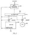
- FIG. 1 is a block diagram illustrating an exemplary implementation of a multi-functional AC to DC converter and its integration into a typical aerospace DC Subsystem according to the present invention
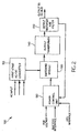
- FIG. 2 is a block diagram of a multi-functional AC to DC converter according to an embodiment of the present invention
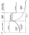
- FIG. 3 is a diagram illustrating the power control stages utilized by a multi-functional AC to DC converter to implement a battery charging control sequence according to an embodiment of the present invention.
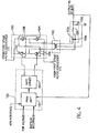
- FIG. 4 is a block diagram of an exemplary DC/DC converter configuration, which is implemented as part of a multifunctional AC to DC converter in accordance with an embodiment of the present invention.
- FIG. 1 illustrates an exemplary implementation of a multi-functional AC to DC converter and its integration into a typical aerospace DC Subsystem according to the present invention.
- a multi-functional converter 100, a battery 200, and an auxiliary power unit 400 are connected to a DC power bus 300, which may be one of multiple DC power buses of an aircraft power subsystem. It should be readily apparent that various electrical loads and other elements may be connected to the DC power bus 300.
- the multi-functional converter 100 receives an AC input (e.g., 115 or 230 Vac) and outputs a voltage that is regulated in accordance with principles of the present invention discussed in detail below.
- a battery current sensor 10 is provided between the DC power bus 300 and the battery 200 to monitor current flow to the battery 200.
- an APU current sensor 20 is provided between the DC power bus 300 and the APU 400 to monitor current flow to the APU 400.
- the multi-functional converter 100 receives the output of the battery current sensor 10 and the APU current sensor 20, as well as the output of a temperature sensor 210, which monitors temperature of the battery 200.
- the multi-functional converter 100 also receives the point-of-regulation ("POR") voltage as an indication of increasing/decreasing load levels on the DC power bus 300.
- POR point-of-regulation
- the multi-functional converter 100 controls output voltage to be within the compliance range of the corresponding DC power subsystem (e.g., within the range of 27.5 to 29 Vdc for aircraft implementation) while adjusting the output voltage to efficiently recharge and prevent electrolyte loss of the battery 200.
- the multi-functional converter 100 adjusts the output voltage during start-up of the APU 400 to limit the starting current of the APU 400 to a level needed for efficient start up.
- the AC to DC converter 100 may independently start the APU 400 or assist a battery in the starting process.
- FIG. 2 is a block diagram of a multi-functional AC to DC converter 100 configuration according to an embodiment of the present invention.
- the multi-functional converter 100 includes: (a) a first stage AC/DC converter 110; (b) a switching module 120; (c) a power control unit 130; (d) an output transformer 140; (e) and an output rectifier and filter unit 150.
- the first stage AC/DC converter receives 3-phase AC voltage (e.g., 115 or 230 Vac at 400 Hz or variable frequency of 360 to 800 Hz) and converts the 3-phase AC voltage to an intermediate DC voltage (e.g., 270 Vdc).
- 3-phase AC voltage e.g., 115 or 230 Vac at 400 Hz or variable frequency of 360 to 800 Hz
- an intermediate DC voltage e.g., 270 Vdc
- This initial AC to DC conversion may be performed by a combination of phase-conversion and rectification circuitry.
- a 3-phase to 9-phase auto-transformer (not shown) may convert the input 3-phase voltage to a 9-phase AC voltage connected to an 1 8-pulse rectifier (not shown) to convert the resulting 9-phase AC voltage to DC voltage.
- the switching module 1 20 converts the DC voltage output by the first stage AC/DC converter 1 10 to an AC voltage based on switch gating signals output by the power control unit 130.
- the switching module 120 may be implemented as a known "H-bridge” configuration of power devices, e.g., insulated gate bipolar transistors ("IGBTs") in which two IGBT pairs are alternatively activated to create an AC voltage across the primary winding of the output transformer 140.
- IGBTs insulated gate bipolar transistors
- the switching control module 120 generates an AC voltage having a root-mean-square ("RMS") level that is controlled by the power-control unit 130 based on one or more of the following: (1) output of the battery current sensor 10; (2) output of the battery temperature sensor 210; (3) output of the APU current sensor 20; and (4) POR voltage, which indicates load on the DC power bus 300.
- RMS root-mean-square
- the AC voltage output by the switching module 1 20 is transformed to a lower AC voltage by the output transformer 140 (i.e., a step-down transformer).
- the lower AC voltage output by the output transformer 140 is rectified and filtered by the output rectifier and filter unit 150 to output a regulated voltage level to the DC power bus 300.
- the regulated voltage output by the output rectifier and filter unit 150 is also fed back to the power control unit 130 to assist regulating voltage to a desired level.
- FIG. 3 illustrates output voltage (solid line) and battery input current (dashed line), as measured by the battery current sensor 10, over a charging cycle of the battery 200.
- the power control unit 130 operates to achieve three recharge stages of the battery 200 while maintaining the output voltage within the compliance range of the DC power bus 300 (e.g., between 27.5 and 29.5 Vdc).
- the power control unit 130 controls the output voltage to a relatively low level (within the compliance range of the power system) that maintains constant limited current flow into the battery 200.
- This power control stage prevents the battery 200 from drawing an uncontrolled or excessive amount of current which could damage the battery or overload the converter 100.
- the power control unit 130 allows the output voltage to increase, thereby maintaining the current flowing to the battery 200 at a constant level.
- the power control unit 130 initiates a second control stage to maintain the output voltage constant at or near the maximum converter output voltage so that the battery 200 continues to charge, albeit at continually decreasing current.
- the charging current into the battery 200 decreases continually due to the increase in the internal battery impedance.
- the power control unit 130 in one implementation of the present invention controls output voltage as a function of battery temperature to optimize the battery charging process, such that the output voltage is made lower for higher battery temperatures and higher for lower battery temperatures. This temperature compensation improves battery charging efficiency.
- the power control unit 130 initiates a third power control stage to lower the output voltage to a nominal regulated level (e.g., 28 Vdc in an aircraft DC bus implementation) to trickle charge the battery (i.e., achieve constant potential trickle charge mode).
- a nominal regulated level e.g., 28 Vdc in an aircraft DC bus implementation
- This voltage level is lower than the one employed during the second control stage in order to minimize the electrolyte loss.
- the charging current into the battery 200 is maintained at a very low level (e.g., 1 amp or less).
- the power control unit 130 can determine within certain limits the level of battery charge and output a signal indicating the estimated charge state of the battery. For example, the power control unit 130 may output a signal to the Flight Deck in an aircraft implementation to indicate readiness of the battery 200 for flight.
- the power control unit 1 30 While controlling the output voltage of the converter 100, the power control unit 1 30 ensures that the output voltage is maintained within a range that is compliant with the requirements of the power quality standard in use for the application. This voltage level enables the battery 200 to be continuously connected to the DC power bus 300. Thus, the battery 200 is readily available during AC power interrupt or other system failures.
- the above-described battery charging stages may be implemented in the power control unit 130 in the form of a dedicated integrated circuit (“IC") card and may be implemented with hardware, software, or a combination of hardware and software.
- the voltage applied may be temperature compensated, e.g., lower for higher battery temperatures and higher when low battery temperatures are measured.
- FIG. 4 illustrates an exemplary configuration for the power control unit 130, the switching module 120, the output transformer 140, and the output rectifier and filter unit 150.
- the power control unit 130 includes a pulse width modulation ("PWM") unit 132 that receives a measure of POR voltage, current measurements for the battery 200 and APU 400, temperature of the battery 200, and a measure of output voltage of the converter 100.
- the PWM unit 132 generates a sequence of pulses, the width of which are varied depending on at least one characteristic of the battery 200 (e.g., depending on the battery charge state).
- the pulse width may further be adjusted to account for changes in load, reflected by the POR voltage, and to account for a start up condition of the APU 400.
- the PWM unit 132 outputs the generated PWM signal to the gate driver 134, which drives the switches of the switching module 120.
- the switching module 120 is a conventional H-bridge configuration of power devices, which are n-channel IGBTs in the exemplary implementation shown in FIG. 4.
- the switching module 120 shown in FIG. 4 includes first, second, third, and fourth IGBT modules 122, 124, 126, and 128, each formed of an IGBT and an anti-parallel diode, the anode of the anti-parallel diode being connected to the emitter of the corresponding IGBT and the cathode being connected to the collector of the corresponding IGBT.
- the gates of the first, second, third, and fourth IGBT modules 122, 124, 126, and 128 are connected to receive an output of the gate driver 134.
- the first IGBT module 122 and the second IGBT module 124 (diagonally positioned) share a common connection to the gate driver 134, thus constituting a first IGBT module pair
- the third IGBT module 126 and the fourth IGBT module 128 (diagonally positioned) share a common connection to the gate driver 134, thus constituting a second IGBT module pair.
- the PWM switching signals output by the gate driver 134 to the IGBT module pairs are offset so that that IGBT module pairs alternately turn ON/OFF, thereby creating an AC voltage across the primary winding of the transformer 140, which is a center-tapped transformer in the exemplary configuration of FIG. 4.
- the collector of the first IGBT module 122 is connected to the (+) output of the first stage AC/DC converter 110.
- the collector of the fourth IGBT module 128 is connected to the (+) output of the first stage AC/DC converter 110.
- the emitter of the first IGBT module 122 is connected to the collector of the third IGBT module 126 and to a first side of the primary winding of the output transformer 140.
- the emitter of the fourth IGBT module 128 is connected to the collector of the second IGBT module 124 and to a second side of the primary winding of the output transformer 140.
- the emitter of the third IGBT module 126 and the emitter of the second IGBT module 124 are connected to the (-) output of the first stage AC/DC converter 110.
- the gate driver 134 By alternately activating two switching module pairs formed of the first and second IGBT modules 122, 124 and the third and fourth IGBT modules 126, 128 respectively, the gate driver 134 causes the switching module 120 to create an alternating voltage across the primary winding of the output transformer 140.
- the RMS value of this alternating voltage is affected by the pulse width of the gating signals output by the gate driver 134, which is altered as a function of at least one of: battery charge characteristics, battery temperature, APU start condition, and POR voltage according to principles of the present invention.
- the output rectifier and filter unit 150 includes a pair of diodes 152a, 152b, each connected to an end of the secondary winding of the output transformer 140 to convert the transformed AC voltage to DC.
- the output rectifier and filter unit 150 further includes an inductor 154 connected between the output of the pair of diodes 152a, 152b and the output of the output rectifier and filter unit 150 and a capacitor 156 connected between the output end of the inductor 1 54 and a negative terminal of the converter arrangement, which is shown as a grounded connection in the implementation of FIG. 4.
- This arrangement of the inductor 1 54 and the capacitor 1 56 filters the rectified DC voltage resulting from the pair of diodes 1 52a, 1 52b. It should be recognized that various alternative arrangements may be suitable for the output rectifier and filter unit 150.
- the power control unit 130 may also continuously monitor the current drawn by the APU 400 (as shown in FIG. 2.)
- the power control unit 130 limits the starting current drawn by the APU 400 to a value which is suitable for the converter 110 to independently start the APU 400 or to start the APU 400 in conjunction with a battery.
- the power control unit 1 30 continuously monitors the POR voltage so as to regulate output voltage as a function of load. Increased load on the DC power bus 300 will cause higher losses to occur in the first stage AC to DC converter 110, which will result in lower RMS voltage applied to the output transformer 140.
- the power control unit 130 adjusts the pulse width for the switch gating signals output to the switching module 120 based on load levels to maintain the desired output voltage of the converter 100.
- the AC to DC converter 100 of the present invention improves reliability because additional Line Replaceable Units ("LRUs") and associated switching devices are not required to connect/disconnect the charging battery 200 to/from the DC power bus 300 and requires less control and power wiring. Furthermore, because the recharging battery 200 may be continuously connected to the DC power bus 300, principles of the present invention enable No-Break-Power-Transfers (NBPT) in the DC subsystem during AC power interrupts or other system failures and reduces DC system weight and cost as compared to a system requiring a separate battery charger.
- NBPT No-Break-Power-Transfers
Abstract
Description
- This invention relates to an AC to DC converter of an electrical power system.
- A conventional power system design includes a Transformer Rectifier Unit ("TRU") as main DC power source, the output voltage of which varies with applied load. Due to the varying nature of its output voltage, the TRU has been considered unsuitable for charging batteries that re relied on for backup/auxiliary power supply. Specifically, the varying nature of the TRU output voltage does not enable a constant potential or constant current charging mode. To address this drawback, some systems use an ON/OFF device to connect and disconnect the battery from the TRU bus to improve charging performance.
- Another conventional approach utilizes a DC generator as a main power source to generate a constant output voltage. Although such a DC generator is suitable for charging batteries at constant potential, this approach can neither limit the current flowing into the battery at the beginning of the starting cycle nor compensate for temperature variations, which strongly influence the battery State of Charge ("SOC"). Also, by not controlling the amount of trickle charge, the DC generator causes the battery to lose electrolytes over time.
- Yet another conventional approach utilizes a Regulated Transformer Rectifier Unit ("RTRU") as a main DC source with constant output voltage: The RTRU can charge batteries at constant potential, but can neither limit the current flowing into the battery nor compensate for temperature variations. Also, by not controlling the amount of trickle charge, the RTRU causes the battery to lose electrolytes over time.
- Due to the above drawbacks, additional equipment, such as a separate battery charger, is commonly used in addition to the main DC power source. Since the charging voltage may be high at times, the battery must be disconnected from the main DC bus of the power system during charging. This requires special power bus arrangements and restricts the use of the battery as a bus presence, thereby affecting DC power system flexibility and quality.
-
US-A-5864221 discloses a multi-functional apparatus for regulating voltage supplied to electrodes and delivered to a rechargeable battery via a bus bar. - The present invention addresses these drawbacks of conventional power system designs by providing a multi-functional apparatus for regulating voltage supplied to electrical loads and delivered to a rechargeable battery via a DC power bus, comprising:
- a AC to DC converter receiving an AC supply voltage, converting said AC supply voltage to a regulated DC voltage, and outputting said regulated DC voltage to said DC power bus, thereby supply said regulated voltage to an electrical load connected to said DC power bus and to said rechargeable battery, which is continuously connected to said DC power bus; and
- a power controller controlling conversion performed by said AC to DC converter as a function of a characteristic of said battery. The present invention is suitable for implementation in an aircraft power system to maintain the voltage output within the compliance range of the DC power bus (e.g., between 27.5 and 29.5 Vdc) while adjusting the output voltage to efficiently charge a battery connected to the bus and/or start an APU connected to the bus.
- In one embodiment of the present invention, a multi-functional AC to DC converter includes a power control unit that monitors the current level drawn by a recharging battery and controls the voltage output by the AC to DC conversion circuitry based on the charging state of the battery. In a first power control stage, in which the battery is completely or nearly discharged, the power control unit controls the output voltage to a relatively low level (within the compliance range of the power system) to prevent the battery from drawing an uncontrolled or excessive amount of current. As the battery charges, and its internal impedance increases, the power control unit allows the output voltage to increase, thereby maintaining the current flowing to the battery at an adequate level for efficiently charging the battery. When the output voltage reaches a threshold level, the power control unit initiates a second control stage to maintain the output voltage constant at the elevated level (e.g., near the upper compliance limit of the DC power bus) so that the battery continues to charge, albeit at continually decreasing current. During this second power control stage, the power control unit in one implementation of the present invention controls output voltage as a function of battery temperature so that the output voltage is lower for higher battery temperatures and higher for lower battery temperatures. This temperature compensation improves the efficiency of the battery charging process. When the current drawn by the battery drops below a threshold level (e.g., indicating that the battery is about 80% percent recharged), the power control unit initiates a third power control stage to lower the output voltage to a nominal regulated level (e.g., 28 Vdc in an aircraft DC bus implementation) to trickle charge the battery (i.e., achieve constant potential trickle charge mode). This third power control stage prevents electrolyte loss during trickle charge.
- By incorporating multiple functions in a single unit, the AC to DC converter of the present invention improves reliability because additional Line Replaceable Units ("LRUs") and associated switching devices are not required to connect/disconnect the charging battery to/from the DC power bus and requires less control and power wiring. Furthermore, because the recharging battery may be continuously connected to the DC power bus, the present invention enables No-Break-Power-Transfers (NBPT) in the DC subsystem during AC power interrupts or other system failures and reduces DC system weight and cost as compared to a system requiring a separate battery charger.
- Other aspects and advantages of the present invention will become apparent upon reading the following detailed description and upon reference to the drawings, in which:
- FIG. 1 is a block diagram illustrating an exemplary implementation of a multi-functional AC to DC converter and its integration into a typical aerospace DC Subsystem according to the present invention;
- FIG. 2 is a block diagram of a multi-functional AC to DC converter according to an embodiment of the present invention;
- FIG. 3 is a diagram illustrating the power control stages utilized by a multi-functional AC to DC converter to implement a battery charging control sequence according to an embodiment of the present invention; and
- FIG. 4 is a block diagram of an exemplary DC/DC converter configuration, which is implemented as part of a multifunctional AC to DC converter in accordance with an embodiment of the present invention.
- FIG. 1 illustrates an exemplary implementation of a multi-functional AC to DC converter and its integration into a typical aerospace DC Subsystem according to the present invention. In the exemplary implementation shown in FIG. 1, a
multi-functional converter 100, abattery 200, and anauxiliary power unit 400 are connected to aDC power bus 300, which may be one of multiple DC power buses of an aircraft power subsystem. It should be readily apparent that various electrical loads and other elements may be connected to theDC power bus 300. Themulti-functional converter 100 receives an AC input (e.g., 115 or 230 Vac) and outputs a voltage that is regulated in accordance with principles of the present invention discussed in detail below. Abattery current sensor 10 is provided between theDC power bus 300 and thebattery 200 to monitor current flow to thebattery 200. Likewise, an APUcurrent sensor 20 is provided between theDC power bus 300 and the APU 400 to monitor current flow to the APU 400. - The
multi-functional converter 100 receives the output of thebattery current sensor 10 and the APUcurrent sensor 20, as well as the output of atemperature sensor 210, which monitors temperature of thebattery 200. Themulti-functional converter 100 also receives the point-of-regulation ("POR") voltage as an indication of increasing/decreasing load levels on theDC power bus 300. As described in detail below, themulti-functional converter 100 controls output voltage to be within the compliance range of the corresponding DC power subsystem (e.g., within the range of 27.5 to 29 Vdc for aircraft implementation) while adjusting the output voltage to efficiently recharge and prevent electrolyte loss of thebattery 200. Furthermore, themulti-functional converter 100 adjusts the output voltage during start-up of theAPU 400 to limit the starting current of theAPU 400 to a level needed for efficient start up. The AC toDC converter 100 may independently start the APU 400 or assist a battery in the starting process. - FIG. 2 is a block diagram of a multi-functional AC to
DC converter 100 configuration according to an embodiment of the present invention. As seen in FIG. 2, themulti-functional converter 100 includes: (a) a first stage AC/DC converter 110; (b) aswitching module 120; (c) apower control unit 130; (d) anoutput transformer 140; (e) and an output rectifier andfilter unit 150. As in a conventional power system design, the first stage AC/DC converter receives 3-phase AC voltage (e.g., 115 or 230 Vac at 400 Hz or variable frequency of 360 to 800 Hz) and converts the 3-phase AC voltage to an intermediate DC voltage (e.g., 270 Vdc). This initial AC to DC conversion may be performed by a combination of phase-conversion and rectification circuitry. For example, a 3-phase to 9-phase auto-transformer (not shown) may convert the input 3-phase voltage to a 9-phase AC voltage connected to an 1 8-pulse rectifier (not shown) to convert the resulting 9-phase AC voltage to DC voltage. It should be apparent that alternative configurations may be utilized to convert the input 3-phase voltage to an intermediate DC voltage. The switching module 1 20 converts the DC voltage output by the first stage AC/DC converter 1 10 to an AC voltage based on switch gating signals output by thepower control unit 130. Theswitching module 120 may be implemented as a known "H-bridge" configuration of power devices, e.g., insulated gate bipolar transistors ("IGBTs") in which two IGBT pairs are alternatively activated to create an AC voltage across the primary winding of theoutput transformer 140. - According to the present invention, the
switching control module 120 generates an AC voltage having a root-mean-square ("RMS") level that is controlled by the power-control unit 130 based on one or more of the following: (1) output of thebattery current sensor 10; (2) output of thebattery temperature sensor 210; (3) output of the APUcurrent sensor 20; and (4) POR voltage, which indicates load on theDC power bus 300. This switching control is discussed in more detail below with reference to FIGS. 3 and 4. The AC voltage output by the switching module 1 20 is transformed to a lower AC voltage by the output transformer 140 (i.e., a step-down transformer). The lower AC voltage output by theoutput transformer 140 is rectified and filtered by the output rectifier andfilter unit 150 to output a regulated voltage level to theDC power bus 300. The regulated voltage output by the output rectifier andfilter unit 150 is also fed back to thepower control unit 130 to assist regulating voltage to a desired level. - Operation of the
power control unit 130 for achieving efficient battery charging will next be described with reference to the diagram of FIG. 3, which illustrates output voltage (solid line) and battery input current (dashed line), as measured by thebattery current sensor 10, over a charging cycle of thebattery 200. As illustrated in FIG. 3, thepower control unit 130 operates to achieve three recharge stages of thebattery 200 while maintaining the output voltage within the compliance range of the DC power bus 300 (e.g., between 27.5 and 29.5 Vdc). In a first power control stage, in which the battery is completely or nearly discharged, thepower control unit 130 controls the output voltage to a relatively low level (within the compliance range of the power system) that maintains constant limited current flow into thebattery 200. This power control stage prevents thebattery 200 from drawing an uncontrolled or excessive amount of current which could damage the battery or overload theconverter 100. - As the
battery 200 charges, and its internal impedance increases, thepower control unit 130 allows the output voltage to increase, thereby maintaining the current flowing to thebattery 200 at a constant level. When the output voltage reaches a maximum threshold level, e.g., just under the upper compliance level of the DC power bus, thepower control unit 130 initiates a second control stage to maintain the output voltage constant at or near the maximum converter output voltage so that thebattery 200 continues to charge, albeit at continually decreasing current. During this second control stage, the charging current into thebattery 200 decreases continually due to the increase in the internal battery impedance. During this second power control stage, thepower control unit 130 in one implementation of the present invention controls output voltage as a function of battery temperature to optimize the battery charging process, such that the output voltage is made lower for higher battery temperatures and higher for lower battery temperatures. This temperature compensation improves battery charging efficiency. - Lastly, when the current drawn by the battery drops below a threshold level (e.g., indicating that the battery is about 80% percent recharged), the
power control unit 130 initiates a third power control stage to lower the output voltage to a nominal regulated level (e.g., 28 Vdc in an aircraft DC bus implementation) to trickle charge the battery (i.e., achieve constant potential trickle charge mode). This voltage level is lower than the one employed during the second control stage in order to minimize the electrolyte loss. During this trickle charge constant voltage stage, the charging current into thebattery 200 is maintained at a very low level (e.g., 1 amp or less). By following changes in battery current and output voltage of theconverter 100 over time, thepower control unit 130 can determine within certain limits the level of battery charge and output a signal indicating the estimated charge state of the battery. For example, thepower control unit 130 may output a signal to the Flight Deck in an aircraft implementation to indicate readiness of thebattery 200 for flight. - While controlling the output voltage of the
converter 100, the power control unit 1 30 ensures that the output voltage is maintained within a range that is compliant with the requirements of the power quality standard in use for the application. This voltage level enables thebattery 200 to be continuously connected to theDC power bus 300. Thus, thebattery 200 is readily available during AC power interrupt or other system failures. The above-described battery charging stages may be implemented in thepower control unit 130 in the form of a dedicated integrated circuit ("IC") card and may be implemented with hardware, software, or a combination of hardware and software. In order to optimize the charging process, the voltage applied may be temperature compensated, e.g., lower for higher battery temperatures and higher when low battery temperatures are measured. - FIG. 4 illustrates an exemplary configuration for the
power control unit 130, theswitching module 120, theoutput transformer 140, and the output rectifier andfilter unit 150. As shown in FIG. 4, thepower control unit 130 includes a pulse width modulation ("PWM")unit 132 that receives a measure of POR voltage, current measurements for thebattery 200 andAPU 400, temperature of thebattery 200, and a measure of output voltage of theconverter 100. ThePWM unit 132 generates a sequence of pulses, the width of which are varied depending on at least one characteristic of the battery 200 (e.g., depending on the battery charge state). The pulse width may further be adjusted to account for changes in load, reflected by the POR voltage, and to account for a start up condition of theAPU 400. ThePWM unit 132 outputs the generated PWM signal to thegate driver 134, which drives the switches of theswitching module 120. - As seen in FIG. 4, the
switching module 120 according to one implementation of the present invention is a conventional H-bridge configuration of power devices, which are n-channel IGBTs in the exemplary implementation shown in FIG. 4. Theswitching module 120 shown in FIG. 4 includes first, second, third, andfourth IGBT modules fourth IGBT modules gate driver 134. Thefirst IGBT module 122 and the second IGBT module 124 (diagonally positioned) share a common connection to thegate driver 134, thus constituting a first IGBT module pair, and thethird IGBT module 126 and the fourth IGBT module 128 (diagonally positioned) share a common connection to thegate driver 134, thus constituting a second IGBT module pair. The PWM switching signals output by thegate driver 134 to the IGBT module pairs are offset so that that IGBT module pairs alternately turn ON/OFF, thereby creating an AC voltage across the primary winding of thetransformer 140, which is a center-tapped transformer in the exemplary configuration of FIG. 4. - As shown in FIG. 4, the collector of the
first IGBT module 122 is connected to the (+) output of the first stage AC/DC converter 110. Likewise, the collector of thefourth IGBT module 128 is connected to the (+) output of the first stage AC/DC converter 110. The emitter of thefirst IGBT module 122 is connected to the collector of thethird IGBT module 126 and to a first side of the primary winding of theoutput transformer 140. The emitter of thefourth IGBT module 128 is connected to the collector of thesecond IGBT module 124 and to a second side of the primary winding of theoutput transformer 140. The emitter of thethird IGBT module 126 and the emitter of thesecond IGBT module 124 are connected to the (-) output of the first stage AC/DC converter 110. By alternately activating two switching module pairs formed of the first andsecond IGBT modules fourth IGBT modules gate driver 134 causes theswitching module 120 to create an alternating voltage across the primary winding of theoutput transformer 140. The RMS value of this alternating voltage is affected by the pulse width of the gating signals output by thegate driver 134, which is altered as a function of at least one of: battery charge characteristics, battery temperature, APU start condition, and POR voltage according to principles of the present invention. - As further shown in FIG. 4, the output rectifier and
filter unit 150 includes a pair ofdiodes output transformer 140 to convert the transformed AC voltage to DC. The output rectifier andfilter unit 150 further includes aninductor 154 connected between the output of the pair ofdiodes filter unit 150 and acapacitor 156 connected between the output end of the inductor 1 54 and a negative terminal of the converter arrangement, which is shown as a grounded connection in the implementation of FIG. 4. This arrangement of the inductor 1 54 and the capacitor 1 56 filters the rectified DC voltage resulting from the pair of diodes 1 52a, 1 52b. It should be recognized that various alternative arrangements may be suitable for the output rectifier andfilter unit 150. - Although operation of the
power control unit 130 has been discussed above based on recharge characteristics of thebattery 200, thepower control unit 130 may also continuously monitor the current drawn by the APU 400 (as shown in FIG. 2.) When used in an APU start application, thepower control unit 130 limits the starting current drawn by theAPU 400 to a value which is suitable for theconverter 110 to independently start theAPU 400 or to start theAPU 400 in conjunction with a battery. As further shown in FIG. 2, the power control unit 1 30 continuously monitors the POR voltage so as to regulate output voltage as a function of load. Increased load on theDC power bus 300 will cause higher losses to occur in the first stage AC toDC converter 110, which will result in lower RMS voltage applied to theoutput transformer 140. Thus, thepower control unit 130 adjusts the pulse width for the switch gating signals output to theswitching module 120 based on load levels to maintain the desired output voltage of theconverter 100. - By incorporating multiple functions in a single unit, the AC to
DC converter 100 of the present invention improves reliability because additional Line Replaceable Units ("LRUs") and associated switching devices are not required to connect/disconnect the chargingbattery 200 to/from theDC power bus 300 and requires less control and power wiring. Furthermore, because the rechargingbattery 200 may be continuously connected to theDC power bus 300, principles of the present invention enable No-Break-Power-Transfers (NBPT) in the DC subsystem during AC power interrupts or other system failures and reduces DC system weight and cost as compared to a system requiring a separate battery charger.
Claims (10)
- A multi-functional apparatus (100) for regulating voltage supplied to electrical loads and delivered to a rechargeable battery (200) via a DC power bus (300), comprising:a AC to DC converter (110, 120, 140, 150) receiving an AC supply voltage, converting said AC supply voltage to a regulated DC voltage, and outputting said regulated DC voltage to said DC power bus (300), thereby supply said regulated voltage to an electrical load connected to said DC power bus and to said rechargeable battery, which is continuously connected to said DC power bus; anda power controller (130) controlling conversion performed by said AC to DC converter (110, 120, 140, 150) as a function of a characteristic of said battery (200.
- The apparatus according to claim 1, wherein said DC power bus (300) is a power bus of an aerospace power system with electrical load connected thereto.
- The apparatus according to claim 1, wherein said power controller (130) controls conversion performed by said AC to DC converter (110, 120, 140, 150) so that said AC to DC converter (110, 120, 140, 150) outputs a DC voltage that maintains a constant current flow into said battery (200) from said DC bus (300) during a first control mode.
- The apparatus according to claim 1, wherein said power controller (130) controls conversion performed by said AC to DC converter (110, 120, 140, 150) so that said AC to DC converter (110, 120, 140, 150) outputs a first constant DC voltage during a second control mode.
- The apparatus according to claim 4, wherein said power controller (130) controls conversion performed by said AC to DC converter (110, 120, 140, 150) so that said AC to DC converter (110, 120, 140, 150) outputs a second constant DC voltage, which is lower than said first constant DC voltage, during a third control mode.
- The apparatus according to claim 1, wherein said AC to DC converter (110, 120, 140, 150) includes:a first AC to DC conversion stage (110) converting said AC supply voltage to an intermediate DC voltage;a switching module 9120) converting said intermediate DC voltage to an intermediate AV voltage;an output transformer (140) transforming said intermediate AV voltage to a step-down AC voltage; anda rectifier (150) converting said step-down AC voltage to a DC voltage.
- The apparatus according to claim 6, wherein said power controller (130) generates a switch gating signal and outputs said switch gating signal to said switching module (120) to control a root-mean-square level of said intermediate AC voltage.
- The apparatus according to claim 7, wherein said power controller (130) generates a pulse width modulated switching signal having a pulse width that varies depending on a recharge state of said battery (200).
- The apparatus according to claim 1, wherein said power controller (130) controls conversion performed by said AC to DC converter (110, 120, 140, 150) as a function of temperature of said battery (200).
- The apparatus according to claim 1, wherein said AC/DC converter (110, 120, 140, 150) outputs said regulated DC voltage to an auxiliary power unit (400) via said DC power bus (300) and said power controller (130) further controls conversion performed by said AC to DC converter (110, 120, 140, 150) as a function of current drawn by said auxiliary power unit (400).
Applications Claiming Priority (5)
| Application Number | Priority Date | Filing Date | Title |
|---|---|---|---|
| US85788 | 1998-05-28 | ||
| US25039000P | 2000-11-30 | 2000-11-30 | |
| US250390P | 2000-11-30 | ||
| US10/085,788 US6577106B2 (en) | 2000-11-30 | 2001-10-19 | Multi-functional AC/DC converter |
| PCT/US2001/044558 WO2002045248A2 (en) | 2000-11-30 | 2001-11-28 | Multi-functional ac/dc converter |
Publications (3)
| Publication Number | Publication Date |
|---|---|
| EP1338075A2 EP1338075A2 (en) | 2003-08-27 |
| EP1338075B1 EP1338075B1 (en) | 2007-10-31 |
| EP1338075B9 true EP1338075B9 (en) | 2008-01-02 |
Family
ID=26773080
Family Applications (1)
| Application Number | Title | Priority Date | Filing Date |
|---|---|---|---|
| EP01999034A Expired - Lifetime EP1338075B9 (en) | 2000-11-30 | 2001-11-28 | Multi-functional ac/dc converter |
Country Status (6)
| Country | Link |
|---|---|
| US (1) | US6577106B2 (en) |
| EP (1) | EP1338075B9 (en) |
| JP (1) | JP2004525590A (en) |
| AT (1) | ATE377279T1 (en) |
| DE (1) | DE60131188T2 (en) |
| WO (1) | WO2002045248A2 (en) |
Families Citing this family (28)
| Publication number | Priority date | Publication date | Assignee | Title |
|---|---|---|---|---|
| US7367193B1 (en) | 2003-07-23 | 2008-05-06 | Hamilton Sundstrand Corporation | Auxiliary power unit control method and system |
| US7417337B1 (en) | 2003-09-04 | 2008-08-26 | Hamilton Sundstrand Corporation | Method and system for facilitating no-break power transfer |
| DE102004016927A1 (en) | 2004-04-06 | 2005-11-03 | Friwo Mobile Power Gmbh | Method for current and voltage regulation for a switching power supply |
| EP1605572A1 (en) * | 2004-06-08 | 2005-12-14 | Friwo Geraetebau GmbH | Battery charger with state of charge determination on the primary side |
| US7358620B2 (en) * | 2004-09-30 | 2008-04-15 | Rockwell Automation Technologies, Inc. | Methods and apparatus for ride-through operation of a complementary device to a transient power source |
| US7112944B1 (en) | 2005-04-19 | 2006-09-26 | Honeywell International Inc. | Electrical power system for multi-use power conditioning and engine start |
| US7583521B2 (en) * | 2006-02-23 | 2009-09-01 | American Power Conversion Corporation | Over voltage clamp |
| US7701082B2 (en) * | 2006-10-30 | 2010-04-20 | Honeywell International Inc. | Aerospace electrical power DC subsystem configuration using multi-functional DC/DC converter |
| US20080123375A1 (en) * | 2006-11-29 | 2008-05-29 | Itt Manufacturing Enterprises, Inc. | Multi-Mode Power Converter |
| US7688048B2 (en) | 2007-02-21 | 2010-03-30 | American Power Conversion Corporation | 3-phase high power UPS |
| US7830686B2 (en) * | 2007-06-05 | 2010-11-09 | Honeywell International Inc. | Isolated high power bi-directional DC-DC converter |
| US8116105B2 (en) | 2008-02-07 | 2012-02-14 | American Power Conversion Corporation | Systems and methods for uninterruptible power supply control |
| US8203294B2 (en) * | 2008-11-25 | 2012-06-19 | GE Aviations Systems LLC | Electric energy storage integrated within or proximate to electrically driven flight control actuators |
| US8112184B2 (en) * | 2009-03-06 | 2012-02-07 | Hamilton Sundstrand Corporation | Auxiliary power unit with dual use of speed signals |
| TWI496378B (en) * | 2009-04-08 | 2015-08-11 | Asustek Comp Inc | Power charging system applied to electronic apparatus |
| US8050069B2 (en) * | 2009-05-29 | 2011-11-01 | General Electric Company | Method and apparatus for electrical bus centering |
| US8385091B2 (en) * | 2009-08-20 | 2013-02-26 | Electric IT Corporation | 3-phase high-power UPS |
| US8503201B2 (en) | 2009-12-03 | 2013-08-06 | Schneider Electric It Corporation | Transient clamping circuitry for voltage converter |
| JP5258831B2 (en) * | 2010-04-21 | 2013-08-07 | 三菱電機株式会社 | Vehicle charging device |
| CN101847890B (en) * | 2010-05-28 | 2012-05-23 | 中达电通股份有限公司 | Control method for enhancing adaptability of communication power supply to single-phase alternating-current power grid |
| US8698354B2 (en) | 2010-11-05 | 2014-04-15 | Schneider Electric It Corporation | System and method for bidirectional DC-AC power conversion |
| WO2014032302A1 (en) | 2012-09-03 | 2014-03-06 | Schneider Electric It Corporation | Method and apparatus for controlling distribution of power |
| US20140265945A1 (en) * | 2013-03-15 | 2014-09-18 | Infineon Technologies Austria Ag | Electric Drive System |
| WO2015112172A1 (en) * | 2014-01-27 | 2015-07-30 | Otis Elevator Company | Charge algorithm for battery propelled elevator |
| US9783317B2 (en) | 2014-08-08 | 2017-10-10 | Honeywell International Inc. | Power converter, generator and architecture for high efficiency auxiliary power unit |
| CN107979150B (en) * | 2016-10-21 | 2024-02-06 | 广州市君盘实业股份有限公司 | Digital control dynamic output charger based on SG3525 chip |
| CN109507506A (en) * | 2018-11-19 | 2019-03-22 | 珠海格力电器股份有限公司 | DC electric apparatus control method and DC electric apparatus |
| US11569753B1 (en) | 2021-10-20 | 2023-01-31 | Honeywell Limited | Apparatuses and methods for an alternating current to direct current converter |
Family Cites Families (20)
| Publication number | Priority date | Publication date | Assignee | Title |
|---|---|---|---|---|
| US4885523A (en) * | 1988-03-15 | 1989-12-05 | Norand Corporation | Battery conditioning system having communication with battery parameter memory means in conjunction with battery conditioning |
| US5019717A (en) | 1988-11-14 | 1991-05-28 | Elegant Design Solutions Inc. | Computer-controlled uninterruptable power supply |
| DE4025322A1 (en) | 1990-08-10 | 1992-02-13 | Thomson Brandt Gmbh | MAINS OPERATED PHASE CONTROL CONTROL |
| US5477132A (en) | 1992-01-10 | 1995-12-19 | Space Systems/Loral, Inc. | Multi-sectioned power converter having current-sharing controller |
| US5481178A (en) | 1993-03-23 | 1996-01-02 | Linear Technology Corporation | Control circuit and method for maintaining high efficiency over broad current ranges in a switching regulator circuit |
| US5606244A (en) | 1993-08-05 | 1997-02-25 | Ofer Energies Ltd. | Mobile AC power source system |
| GB9400499D0 (en) | 1994-01-12 | 1994-03-09 | Magnum Power Solutions Ltd | Improved uninterruptible power supply |
| US5761057A (en) | 1995-03-09 | 1998-06-02 | Thomson Consumer Electronics, Inc. | Switched mode power supply with synchronous preconverter |
| US5754414A (en) | 1996-02-23 | 1998-05-19 | Hanington; Gary J. | Self-compensating switching power converter |
| DE19616409A1 (en) | 1996-04-24 | 1997-10-30 | Patent Treuhand Ges Fuer Elektrische Gluehlampen Mbh | Electric lamp |
| US5783872A (en) | 1996-07-25 | 1998-07-21 | Northrop Grumman Corporation | Auxiliary battery voltage/temperature compensation for automotive 12 volt system for electric vehicles |
| US5920162A (en) | 1996-08-05 | 1999-07-06 | Sundstrand Corporation | Position control using variable exciter feed through |
| EP0941570A1 (en) | 1996-08-30 | 1999-09-15 | Sgs-Thomson Microelectronics | Method and apparatus for automatic average current mode controlled power factor correction without input voltage sensing |
| US6104172A (en) | 1997-07-01 | 2000-08-15 | Power-One | Power factor corrector |
| US5864221A (en) | 1997-07-29 | 1999-01-26 | Trw Inc. | Dedicated avionics standby power supply |
| US6154015A (en) | 1998-07-14 | 2000-11-28 | Ricoh Company, Ltd. | DC-DC converter |
| US6023158A (en) | 1998-11-10 | 2000-02-08 | Lucent Technologies Inc. | Switch drive controller, method of operation thereof and power converter employing the same |
| US6091233A (en) | 1999-01-14 | 2000-07-18 | Micro Linear Corporation | Interleaved zero current switching in a power factor correction boost converter |
| US6075352A (en) | 1999-01-22 | 2000-06-13 | Dell Computer Corporation | Redirected sequential flyback synchronous rectifier |
| US6101106A (en) | 1999-02-05 | 2000-08-08 | The Boeing Company | Pulse width modulated controller for high temperature power conversion |
-
2001
- 2001-10-19 US US10/085,788 patent/US6577106B2/en not_active Expired - Fee Related
- 2001-11-28 AT AT01999034T patent/ATE377279T1/en not_active IP Right Cessation
- 2001-11-28 WO PCT/US2001/044558 patent/WO2002045248A2/en active IP Right Grant
- 2001-11-28 JP JP2002546276A patent/JP2004525590A/en active Pending
- 2001-11-28 EP EP01999034A patent/EP1338075B9/en not_active Expired - Lifetime
- 2001-11-28 DE DE60131188T patent/DE60131188T2/en not_active Expired - Fee Related
Also Published As
| Publication number | Publication date |
|---|---|
| US6577106B2 (en) | 2003-06-10 |
| US20020126518A1 (en) | 2002-09-12 |
| DE60131188T2 (en) | 2008-08-07 |
| DE60131188D1 (en) | 2007-12-13 |
| WO2002045248A2 (en) | 2002-06-06 |
| JP2004525590A (en) | 2004-08-19 |
| WO2002045248A3 (en) | 2002-08-15 |
| EP1338075A2 (en) | 2003-08-27 |
| ATE377279T1 (en) | 2007-11-15 |
| EP1338075B1 (en) | 2007-10-31 |
Similar Documents
| Publication | Publication Date | Title |
|---|---|---|
| EP1338075B1 (en) | Multi-functional ac/dc converter | |
| JP3821230B2 (en) | Coupled AC-DC / Converter | |
| US5483436A (en) | Gate drive power supply operable from a source of unregulated DC electric power | |
| US4985671A (en) | Power supply circuit for a motor vehicle with two load voltages | |
| US20030160514A1 (en) | Universal uninterruptible power supply input circuitry and methods for configuring same | |
| WO2003071668A1 (en) | Alternator/inverter with dual h-bridge and automatic voltage regulation | |
| CN106961150B (en) | Control method and system of composite energy storage battery | |
| EP3937363A1 (en) | Inverter of photovoltaic grid-connected power generation system, starting device and method, and system | |
| US20230344235A1 (en) | Energy storage system | |
| US11601006B2 (en) | Control of DC voltage distribution system | |
| EP3989380A2 (en) | A novel method to overcome electrical circuit voltage and current limitations | |
| US5933331A (en) | Battery coupling apparatus | |
| US10998759B2 (en) | Uninterruptible power supply with DC output | |
| JP3330232B2 (en) | AC / DC uninterruptible power supply | |
| US10700540B2 (en) | DC power supply system | |
| CA3019619C (en) | Power supply connection device, and charging-discharging control method for same | |
| JPH04372537A (en) | Composite input station | |
| EP3975411B1 (en) | Rectifier, charging system and electric vehicle | |
| JP6707309B2 (en) | Power supply system | |
| KR100443427B1 (en) | Uninterruptible Power Supply Apparatus | |
| WO2021010288A1 (en) | Synchronous generator control device and electricity supply system provided with same | |
| CN220754413U (en) | AC power supply circuit and inverter auxiliary power supply system | |
| JPH02164236A (en) | Uninterruptible power supply | |
| JPH076679Y2 (en) | Power supply equipment | |
| CN117118001A (en) | Charging and discharging system with long service life and energy storage device |
Legal Events
| Date | Code | Title | Description |
|---|---|---|---|
| PUAI | Public reference made under article 153(3) epc to a published international application that has entered the european phase |
Free format text: ORIGINAL CODE: 0009012 |
|
| 17P | Request for examination filed |
Effective date: 20030609 |
|
| AK | Designated contracting states |
Designated state(s): AT BE CH CY DE DK ES FI FR GB GR IE IT LI LU MC NL PT SE TR |
|
| 17Q | First examination report despatched |
Effective date: 20040309 |
|
| GRAP | Despatch of communication of intention to grant a patent |
Free format text: ORIGINAL CODE: EPIDOSNIGR1 |
|
| GRAS | Grant fee paid |
Free format text: ORIGINAL CODE: EPIDOSNIGR3 |
|
| GRAA | (expected) grant |
Free format text: ORIGINAL CODE: 0009210 |
|
| AK | Designated contracting states |
Kind code of ref document: B1 Designated state(s): AT BE CH CY DE DK ES FI FR GB GR IE IT LI LU MC NL PT SE TR |
|
| REG | Reference to a national code |
Ref country code: GB Ref legal event code: FG4D |
|
| REG | Reference to a national code |
Ref country code: IE Ref legal event code: FG4D |
|
| REG | Reference to a national code |
Ref country code: CH Ref legal event code: EP |
|
| REF | Corresponds to: |
Ref document number: 60131188 Country of ref document: DE Date of ref document: 20071213 Kind code of ref document: P |
|
| NLV1 | Nl: lapsed or annulled due to failure to fulfill the requirements of art. 29p and 29m of the patents act | ||
| PG25 | Lapsed in a contracting state [announced via postgrant information from national office to epo] |
Ref country code: CH Free format text: LAPSE BECAUSE OF FAILURE TO SUBMIT A TRANSLATION OF THE DESCRIPTION OR TO PAY THE FEE WITHIN THE PRESCRIBED TIME-LIMIT Effective date: 20071031 Ref country code: SE Free format text: LAPSE BECAUSE OF FAILURE TO SUBMIT A TRANSLATION OF THE DESCRIPTION OR TO PAY THE FEE WITHIN THE PRESCRIBED TIME-LIMIT Effective date: 20080131 Ref country code: NL Free format text: LAPSE BECAUSE OF FAILURE TO SUBMIT A TRANSLATION OF THE DESCRIPTION OR TO PAY THE FEE WITHIN THE PRESCRIBED TIME-LIMIT Effective date: 20071031 Ref country code: ES Free format text: LAPSE BECAUSE OF FAILURE TO SUBMIT A TRANSLATION OF THE DESCRIPTION OR TO PAY THE FEE WITHIN THE PRESCRIBED TIME-LIMIT Effective date: 20080211 Ref country code: LI Free format text: LAPSE BECAUSE OF FAILURE TO SUBMIT A TRANSLATION OF THE DESCRIPTION OR TO PAY THE FEE WITHIN THE PRESCRIBED TIME-LIMIT Effective date: 20071031 |
|
| ET | Fr: translation filed | ||
| REG | Reference to a national code |
Ref country code: CH Ref legal event code: PL |
|
| PG25 | Lapsed in a contracting state [announced via postgrant information from national office to epo] |
Ref country code: PT Free format text: LAPSE BECAUSE OF FAILURE TO SUBMIT A TRANSLATION OF THE DESCRIPTION OR TO PAY THE FEE WITHIN THE PRESCRIBED TIME-LIMIT Effective date: 20080331 |
|
| PG25 | Lapsed in a contracting state [announced via postgrant information from national office to epo] |
Ref country code: MC Free format text: LAPSE BECAUSE OF NON-PAYMENT OF DUE FEES Effective date: 20071130 Ref country code: AT Free format text: LAPSE BECAUSE OF FAILURE TO SUBMIT A TRANSLATION OF THE DESCRIPTION OR TO PAY THE FEE WITHIN THE PRESCRIBED TIME-LIMIT Effective date: 20071031 |
|
| PG25 | Lapsed in a contracting state [announced via postgrant information from national office to epo] |
Ref country code: DK Free format text: LAPSE BECAUSE OF FAILURE TO SUBMIT A TRANSLATION OF THE DESCRIPTION OR TO PAY THE FEE WITHIN THE PRESCRIBED TIME-LIMIT Effective date: 20071031 |
|
| PG25 | Lapsed in a contracting state [announced via postgrant information from national office to epo] |
Ref country code: BE Free format text: LAPSE BECAUSE OF FAILURE TO SUBMIT A TRANSLATION OF THE DESCRIPTION OR TO PAY THE FEE WITHIN THE PRESCRIBED TIME-LIMIT Effective date: 20071031 |
|
| PLBE | No opposition filed within time limit |
Free format text: ORIGINAL CODE: 0009261 |
|
| STAA | Information on the status of an ep patent application or granted ep patent |
Free format text: STATUS: NO OPPOSITION FILED WITHIN TIME LIMIT |
|
| 26N | No opposition filed |
Effective date: 20080801 |
|
| PG25 | Lapsed in a contracting state [announced via postgrant information from national office to epo] |
Ref country code: IE Free format text: LAPSE BECAUSE OF NON-PAYMENT OF DUE FEES Effective date: 20071128 |
|
| PG25 | Lapsed in a contracting state [announced via postgrant information from national office to epo] |
Ref country code: GR Free format text: LAPSE BECAUSE OF FAILURE TO SUBMIT A TRANSLATION OF THE DESCRIPTION OR TO PAY THE FEE WITHIN THE PRESCRIBED TIME-LIMIT Effective date: 20080201 |
|
| PG25 | Lapsed in a contracting state [announced via postgrant information from national office to epo] |
Ref country code: FI Free format text: LAPSE BECAUSE OF FAILURE TO SUBMIT A TRANSLATION OF THE DESCRIPTION OR TO PAY THE FEE WITHIN THE PRESCRIBED TIME-LIMIT Effective date: 20071031 |
|
| PGFP | Annual fee paid to national office [announced via postgrant information from national office to epo] |
Ref country code: FR Payment date: 20081106 Year of fee payment: 8 |
|
| PGFP | Annual fee paid to national office [announced via postgrant information from national office to epo] |
Ref country code: DE Payment date: 20081128 Year of fee payment: 8 |
|
| PG25 | Lapsed in a contracting state [announced via postgrant information from national office to epo] |
Ref country code: CY Free format text: LAPSE BECAUSE OF FAILURE TO SUBMIT A TRANSLATION OF THE DESCRIPTION OR TO PAY THE FEE WITHIN THE PRESCRIBED TIME-LIMIT Effective date: 20071031 |
|
| PG25 | Lapsed in a contracting state [announced via postgrant information from national office to epo] |
Ref country code: LU Free format text: LAPSE BECAUSE OF NON-PAYMENT OF DUE FEES Effective date: 20071128 |
|
| PG25 | Lapsed in a contracting state [announced via postgrant information from national office to epo] |
Ref country code: TR Free format text: LAPSE BECAUSE OF FAILURE TO SUBMIT A TRANSLATION OF THE DESCRIPTION OR TO PAY THE FEE WITHIN THE PRESCRIBED TIME-LIMIT Effective date: 20071031 |
|
| PGFP | Annual fee paid to national office [announced via postgrant information from national office to epo] |
Ref country code: GB Payment date: 20091007 Year of fee payment: 9 |
|
| REG | Reference to a national code |
Ref country code: FR Ref legal event code: ST Effective date: 20100730 |
|
| PG25 | Lapsed in a contracting state [announced via postgrant information from national office to epo] |
Ref country code: FR Free format text: LAPSE BECAUSE OF NON-PAYMENT OF DUE FEES Effective date: 20091130 |
|
| PG25 | Lapsed in a contracting state [announced via postgrant information from national office to epo] |
Ref country code: DE Free format text: LAPSE BECAUSE OF NON-PAYMENT OF DUE FEES Effective date: 20100601 |
|
| PG25 | Lapsed in a contracting state [announced via postgrant information from national office to epo] |
Ref country code: IT Free format text: LAPSE BECAUSE OF NON-PAYMENT OF DUE FEES Effective date: 20071130 |
|
| GBPC | Gb: european patent ceased through non-payment of renewal fee |
Effective date: 20101128 |
|
| PG25 | Lapsed in a contracting state [announced via postgrant information from national office to epo] |
Ref country code: GB Free format text: LAPSE BECAUSE OF NON-PAYMENT OF DUE FEES Effective date: 20101128 |
|
| P01 | Opt-out of the competence of the unified patent court (upc) registered |
Effective date: 20230525 |