TECHNICAL FIELD
-
The present invention relates to a method for
identifying a semiconductor integrated circuit device,
a method for manufacturing a semiconductor integrated
circuit device, a semiconductor integrated circuit
device and a semiconductor chip, and mainly relates to
the technology for assigning identification information
unique to semiconductor integrated circuit devices or
semiconductor chips to identify individual semiconductor
integrated circuit devices or semiconductor chips.
BACKGROUND ART
-
A semiconductor integrated circuit device can
be utilized in a variety of desired manners based on
identification information unique thereto, if such
identification information is assigned. If unique
identification information can be set to semiconductor
integrated circuit devices on a one-by-one basis, a
novel manufacturing method and product management
technique, demonstrated by the inventors, can be
provided under the utilization of the unique identification
information, as described later.
-
When a fault occurs at a stage such as an
actual use stage of a semiconductor integrated circuit
device, factors causing the fault is readily pursued if
unique identification information can be retrieved from
the semiconductor integrated circuit device. For
example, a semiconductor maker can acquire information
such as the manufacturing term, manufacturing line,
manufacturing lot, testing history, design information
and the like based on the unique identification
information of the semiconductor integrated circuit
device. This facilitates the pursuit of factors which
cause the fault and countermeasures to be taken
therefor.
-
The marking based on an ink printing method
or a laser impressing method given to a package, which
forms part of a semiconductor integrated circuit
device, can be regarded as one type of identification
information. While this type of marking mainly
comprises a product model name of the semiconductor
integrated circuit device, the product model name may
be accompanied by a code representation of the
manufacturing term such as year, week and the like.
However, with this type of marking representation, it
is difficult to set unique identification information
to semiconductor integrated circuit devices on a one-by-one
basis, which can be manufactured in large
quantity or manufactured over a long term as industrial
products, due to the shortage of the amount of information
which can be represented thereby.
-
It can be assumed to set a programmable
element such as a fuse element to a semiconductor chip
which forms part of a semiconductor integrated circuit
device and to give unique identification information
inherent to the programmable element. However, if the
original semiconductor integrated circuit device does
not need a program element, this type of assumable
technique would disadvantageously cause a complicated
manufacturing process and an increased cost of the
semiconductor integrated circuit device due to the
requirement for an additional manufacturing step for
the programmable element. The manufacturing process
will be free from additional complication if the
semiconductor integrated circuit device originally has
a programmable element. Even in this case, an
additional or modified manufacturing step is needed for
writing unique recognition information into the
programmable element.
-
In a know technique referred to as "silicon
signature," a product model name or unique information
is written into a semiconductor integrated circuit
device in such a manner that they can be electrically
read out. However, this type of technique requires an
additional or modified manufacturing step for writing
the information, as is the case with the foregoing.
-
The inventors were informed, through an
investigation after the present invention had been
made, that inventions described in JP-A-6-196435, JP-A-10-055939,
JP-A-11-214274, JP-A-7-335509, and JP-A-7-050233
existed as related to the present invention,
later described. Either of the inventions described in
the official documents is recognized to require an
extra manufacturing step for writing unique identification
information into each chip. However, these
official documents are not recognized to include any
description related to a method for identifying a
semiconductor integrated circuit device which does not
particularly require an additional or a modified
manufacturing step as the present invention, later
described.
-
It is therefore an object of the present
invention to provide a semiconductor integrated circuit
device or a semiconductor chip which can be individually
identified in a simple configuration, and a method
for identifying a semiconductor integrated circuit
device or a semiconductor chip. It is another object
of the present invention to provide a semiconductor
integrated circuit device which is capable of
identifying individual semiconductor integrated circuit
devices or semiconductor chips with a high reliability.
It is a further object of the present invention to
provide a rational method for manufacturing a
semiconductor integrated circuit device. The above and
other objects and novel features of the present
invention will become apparent from the description of
the specification and the accompanying drawings.
DISCLOSURE OF THE INVENTION
-
Representatives of the inventions disclosed
in this application are briefly described in summary as
follows. Specifically, in course of a manufacturing
process of semiconductor integrated circuit devices, a
plurality of identification elements having the same
arrangement are formed and the relation of magnitude in
a physical amount corresponding to variations in the
process of the plurality of identification elements is
employed as the basis for identification information
unique to the semiconductor integrated circuit device.
BRIEF DESCRIPTION OF THE DRAWINGS
-
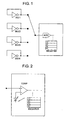
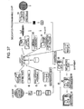
- Fig. 1 is a basic circuit diagram
illustrating one embodiment of an identification number
generator circuit according to the present invention;
- Fig. 2 is a basic circuit diagram
illustrating another embodiment of the identification
number generator circuit according to the present
invention;
- Fig. 3 is a basic circuit diagram
illustrating another embodiment of the identification
number generator circuit according to the present
invention;
- Fig. 4 is a diagram for describing the
operation of the identification number generator
circuit of Fig. 3;
- Fig. 5 is a basic circuit diagram
illustrating another embodiment of the identification
number generator circuit according to the present
invention;
- Fig. 6 is an equivalent circuit diagram for
describing the circuit in the embodiment of Fig. 5;
- Fig. 7 is a circuit diagram illustrating a
specific embodiment corresponding to the embodiment of
Fig. 5;
- Fig. 8 is a timing chart for describing the
operation of the circuit in the embodiment of Fig. 7;
- Fig. 9 is a diagram for describing the
operation of the circuit in the embodiment of Fig. 7;
- Fig. 10 is an exemplary modification
illustrating one embodiment of a unit circuit which
comprises a CMOS inverter circuit and switch MOSFETs
which are the core of the identification number
generator circuit according to the present invention;
- Fig. 11 is an exemplary modification
illustrating another embodiment of the unit circuit
which comprises a CMOS inverter circuit and switch
MOSFETs which are the core of the identification number
generator circuit according to the present invention;
- Fig. 12 is an exemplary modification
illustrating another embodiment of the unit circuit
which comprises a CMOS inverter circuit and switch
MOSFETs which are the core of the identification number
generator circuit according to the present invention;
- Fig. 13 is an exemplary modification
illustrating another embodiment of the unit circuit
which comprises a CMOS inverter circuit and switch
MOSFETs which are the core of the identification number
generator circuit according to the present invention;
- Fig. 14 is an exemplary modification
illustrating another embodiment of the unit circuit
which comprises a CMOS inverter circuit and switch
MOSFETs which are the core of the identification number
generator circuit according to the present invention;
- Fig. 15 is an exemplary modification
illustrating another embodiment of the unit circuit
which comprises a CMOS inverter circuit and switch
MOSFETs which are the core of the identification number
generator circuit according to the present invention;
- Fig. 16 is a circuit diagram illustrating one
embodiment of a CMOS inverter circuit used in the
identification number generator circuit according to
the present invention;
- Fig. 17 is a circuit diagram illustrating
another embodiment of the identification number
generator circuit according to the present invention;
- Fig. 18 is a waveform chart for describing
the operation of the circuit in the embodiment
illustrated in Fig. 17;
- Fig. 19 is a block diagram illustrating
another embodiment of the identification number
generator circuit according to the present invention;
- Fig. 20 is a block diagram illustrating
another embodiment of the identification number
generator circuit according to the present invention;
- Fig. 21 is a general block diagram
illustrating one embodiment of a semiconductor
integrated circuit device according to the present
invention;
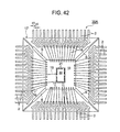
- Fig. 22 is an element layout diagram
illustrating one embodiment of the semiconductor
integrated circuit device according to the present
invention;
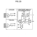
- Fig. 23 is an equivalent circuit diagram
corresponding to the foregoing Fig. 22;
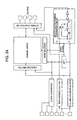
- Fig. 24 is a block diagram illustrating one
embodiment in which the present invention is applied to
dynamic RAM;
- Fig. 25 is a general schematic diagram
illustrating one embodiment of a semiconductor
integrated circuit device which employs the
identification number generator circuit according to
the present invention;
- Fig. 26 is an explanatory diagram for
explaining an algorithm for identifying an identification
number according to the present invention;
- Fig. 27 is an explanatory diagram for
explaining an algorithm for identifying an identification
number according to the present invention;
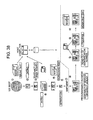
- Fig. 28 is a schematic diagram illustrating
one embodiment of a method of registering a matching
algorithm in a system for identifying a semiconductor
integrated circuit device according to the present
invention;
- Fig. 29 is a schematic diagram illustrating
one embodiment of the method of registering a matching
algorithm in the system for identifying a semiconductor
integrated circuit device according to the present
invention;
- Fig. 30 is an explanatory diagram showing an
exemplary comparison method in the foregoing Fig. 29;
- Fig. 31 is an explanatory diagram showing a
comparison method when using the order of logical
threshold values in a CMOS inverter circuit;
- Fig. 32 is an explanatory diagram showing a
comparison method when using the order of logical
threshold values in the CMOS inverter circuit;
- Fig. 33 is a schematic diagram illustrating
one embodiment of a semiconductor integrated circuit
device to which the present invention is applied;
- Fig. 34 is a block diagram illustrating one
embodiment of a multi-chip module to which the present
invention is applied;
- Fig. 35 is a block diagram illustrating one
embodiment of a dedicated program chip in the foregoing
Fig. 34;
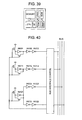
- Fig. 36 is a schematic diagram for describing
a manufacturing step of one embodiment of a semiconductor
integrated circuit device which is mounted with the
identification number generator circuit according to
this application;
- Fig. 37 is a schematic diagram for describing
a manufacturing step of one embodiment when a
semiconductor integrated circuit device mounted with
the identification number generator circuit according
to this application is assembled into a circuit
mounting board;
- Fig. 38 is a schematic diagram for describing
a manufacturing step of another embodiment of the
semiconductor integrated circuit device which mounted
with the identification number generator circuit
according to this application;
- Fig. 39 is a block diagram illustrating an
exemplary application specific LSI which is provided
with the identification number generator circuit
according to the present invention;
- Fig. 40 is a circuit diagram illustrating an
embodiment in which variations in logical threshold
value of the CMOS inverter according to the present
invention is applied to a random number generator;
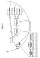
- Fig. 41 is a schematic diagram for describing
an exemplary use of a chip identification number
generator circuit for purposes of reducing fraudulent
actions and a variety of troubles in an inter-enterprise
electronic part procurement market;
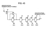
- Fig. 42 is a basic circuit diagram
illustrating another embodiment of the identification
number generator circuit according to the present
invention;
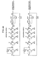
- Fig. 43 is a basic circuit diagram
illustrating another embodiment of the identification
number generator circuit according to the present
invention;
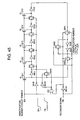
- Fig. 44 is a basic circuit diagram
illustrating another embodiment of the identification
number generator circuit according to the present
invention;
- Fig. 45 is a specific circuit diagram
illustrating one embodiment of the identification
number generator circuit according to the present
invention;
- Fig. 46 is a specific circuit diagram
illustrating a further embodiment of the identification
number generator circuit according to the present
invention;
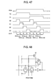
- Fig. 47 is a timing diagram for describing
the operation of the circuit in the embodiment of Fig.
46;
- Fig. 48 is a circuit diagram illustrating
another embodiment of the unit circuit used in the
embodiment of the foregoing Fig. 46;
- Fig. 49 is a circuit diagram illustrating a
further embodiment of the identification number
generator circuit according to the present invention;
- Fig. 50 is a circuit diagram illustrating a
further embodiment of the identification number
generator circuit according to the present invention;
- Fig. 51 is a circuit layout diagram
illustrating one embodiment of a semiconductor
integrated circuit device or a semiconductor chip to
which the present invention is applied;
- Fig. 52 is a block diagram illustrating a
standard embodiment of the I/O cell;
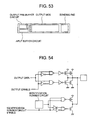
- Fig. 53 is a circuit layout diagram
illustrating one embodiment of an I/O cell provided in
a semiconductor integrated circuit device or a
semiconductor chip according to the present invention;
- Fig. 54 is a circuit diagram illustrating one
embodiment of an output buffer circuit which is
provided in a semiconductor integrated circuit device
or a semiconductor chip according to the present
invention;
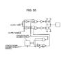
- Fig. 55 is a circuit diagram illustrating
another embodiment of an output buffer circuit which is
provided in a semiconductor integrated circuit device
or a semiconductor chip according to the present
invention;
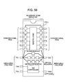
- Fig. 56 is a general schematic diagram
illustrating one embodiment of a semiconductor
integrated circuit device according to the present
invention;
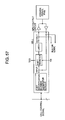
- Fig. 57 is a block diagram illustrating one
embodiment of a basic JTAG cell for the semiconductor
integrated circuit device according to the present
invention;
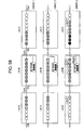
- Fig. 58 is a schematic diagram for describing
one embodiment of an operation of serially outputting
an identification number, making use of a shifting
operation of a boundary scan register of the
semiconductor integrated circuit device according to
the present invention;
- Fig. 59 is a schematic diagram for describing
another embodiment of the operation of serially
outputting an identification number, making use of the
shift operation of the boundary scan register of the
semiconductor integrated circuit device according to
the present invention;
- Fig. 60 is a schematic diagram for describing
another embodiment of the operation of serially
outputting an identification number, making use of a
shifting operation of a boundary scan register of the
semiconductor integrated circuit device according to
the present invention;
- Fig. 61 is a schematic diagram for describing
another embodiment of the operation of serially
outputting an identification number, making use of the
shift operation of the boundary scan register of the
semiconductor integrated circuit device according to
the present invention;
- Fig. 62 is a circuit diagram illustrating a
further embodiment of the identification number
generator circuit according to the present invention;
- Fig. 63 is an explanatory diagram of an
identification number according to the present
invention;
- Fig. 64 is an explanatory diagram of the
identification number according to the present
invention;
- Fig. 65 is a flow chart for describing one
embodiment of a fast identification number matching
(searching) algorithm for an identification number
generated by the identification number generator
circuit according to the present invention;
- Fig. 66 is a schematic diagram corresponding
to the embodiment of Fig. 65;
- Fig. 67 is a flow chart illustrating one
embodiment of a method for designing circuits for a
semiconductor chip which incorporates the
identification number generator circuit according to
the present invention;
- Fig. 68 is a flow chart illustrating one
embodiment of a method for designing an LSI which has
the built-in identification number generator circuit
according to the present invention;
- Fig. 69 illustrates a flow chart of one
embodiment of a method for manufacturing a
semiconductor integrated circuit device which uses a
semiconductor chip with a built-in identification
number generator circuit according to the present
invention;
- Fig. 70 is a flow chart illustrating one
embodiment of a process of assembling a semiconductor
integrated circuit device which uses a semiconductor
chip mounted with the identification number generator
circuit according to the present invention;
- Fig. 71 is a schematic diagram illustrating
one embodiment of a method of reducing the number of
bits of the identification number generator circuit
according to the present invention;
- Fig. 72 is a schematic diagram illustrating
one embodiment of a method of reducing the number of
bits of the identification number generator circuit
according to the present invention;
- Fig. 73 is a schematic diagram for describing
a testing method which utilizes the identification
number generator circuit mounted in the semiconductor
integrated circuit device according to the present
invention;
- Fig. 74 is a schematic diagram for describing
the testing method which utilizes the identification
number generator circuit mounted in the semiconductor
integrated circuit device according to the present
invention;
- Fig. 75 is a schematic diagram for describing
a method for managing correlation of characteristic
data for each semiconductor chip in each test step,
making use of the identification number generator
circuit mounted in the semiconductor integrated circuit
device according to the present invention;
- Fig. 76 is a schematic diagram for describing
a method for automatically managing wafers in a pre-process,
making use of the identification number
generator circuit mounted in the semiconductor
integrated circuit device according to the present
invention;
- Fig. 77 is a schematic diagram for describing
a method of storing and searching an identification
number of the identification number generator circuit
mounted in the semiconductor integrated circuit device
according to the present invention;
- Fig. 78 is a schematic diagram for describing
another example of the method of storing and searching
an identification number of the identification number
generator circuit mounted in the semiconductor
integrated circuit device according to the present
invention;
- Fig. 79 is a schematic diagram illustrating
one embodiment of a method for recovering a
semiconductor integrated circuit device, making use of
the identification number generator circuit according
to the present invention;
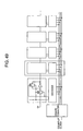
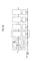
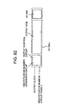
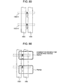
- Fig. 80 is a layout diagram illustrating one
embodiment of a semiconductor integrated circuit device
which is mounted with the identification number
generator circuit according to the present invention;
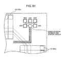
- Fig. 81 is a partially enlarged layout
diagram of the layout diagram in Fig. 80;
- Fig. 82 is a layout diagram illustrating
another embodiment of the semiconductor integrated
circuit device which is mounted with the identification
number generator circuit according to the present
invention;
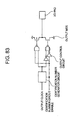
- Fig. 83 is a circuit diagram corresponding to
the layout in Fig. 81;
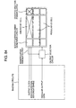
- Fig. 84 is a schematic diagram illustrating a
further embodiment of the semiconductor integrated
circuit device which comprises the identification
number generator circuit according to the present
invention;
- Fig. 85 is a partially plan pattern diagram
of a semiconductor integrated circuit device which
forms part of the embodiment in Fig. 84;
- Fig. 86 is another partially plan pattern
diagram of the semiconductor integrated circuit device
which forms part of the embodiment in Fig. 84; and
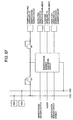
- Fig. 87 is a circuit diagram illustrating one
embodiment of the semiconductor integrated circuit
device which comprises the identification number
generator circuit according to the present invention.
-
BEST MODE FOR CARRYING OUT THE INVENTION
-
For discussing the present invention in
greater detail, the invention will be described with
reference to the accompanying drawings.
-
Fig. 1 illustrates a basic circuit diagram of
one embodiment of an identification number generator
circuit according to the present invention. CMOS
inverter circuits INV1 to INV4 are configured to have
the same characteristics as one another within an
actually controllable range on the design and
manufacturing of a semiconductor integrated circuit
device. A specific configuration suitable for the
present invention in order to provide a plurality of
inverters with the same characteristics as one another
will be better understood with reference to later Fig.
22 and description thereon. Therefore, a technique for
providing the same characteristics as one another will
be generally described below.
-
In a CMOS inverter circuit, it is understood
that its characteristics are generally determined by
the relative conductance of a P-channel MOSFET and an
N-channel MOSFET which comprise the CMOS inverter
circuit. In this respect, it can be understood that
CMOS inverters having the same characteristics can be
implemented by MOSFETs which have the same ratio W/L of
a channel width W to a channel length L but have
different sizes. However, the influence on the
electric characteristics due to variations in
semiconductor integrated circuit devices during the
manufacturing is different for elements of different
sizes.
-
In the embodiment, preferably, the plurality
of CMOS inverters INV1 to INV4 are each implemented by
elements, forming parts of the respective CMOS
inverter, which have the same structure and the same
size as one another. It goes without saying that these
elements are manufactured in accordance with the
characteristics of semiconductor integrated circuit
devices which are manufactured in batches under the
same process. In this way, the plurality of CMOS
inverters INV1 to INV4 uniformly suffer from the
influence due to manufacturing variations such as
variations in machining dimensions during the
manufacturing of semiconductor integrated circuit
devices, variations in thicknesses of various layers,
variations in impurity concentrations, and the like.
-
In the CMOS inverter circuit which has short-circuited
input and output as illustrated in Fig. 1, an
output voltage reaches a logical threshold value
voltage. When all the CMOS inverter circuits have
completely the same electric characteristics, the four
inverter circuits INV1 to INV4 have an equal potential
at a short-circuited node. However, this is an ideal
condition, and in an actual semiconductor device,
slight differences in the characteristics result in a
difference in the potential at the input/output short-circuited
nodes of the respective inverter circuits
INV1 to INV4, i.e., the logical threshold value
voltage.
-
It may be understood that the variations in
the logical threshold value in the CMOS inverter
circuits are dominated by variations in the MOS
transistor characteristics. Also, the cause for the
variations in the MOS transistor characteristics can be
the gate width of the MOS transistor, the film
thickness of a gate insulating film, a conduction
determinant impurity concentration, its distribution,
and the like. These variations can be classified into
a macroscopic aspect and a microscopic aspect. The
macroscopic aspect includes variations in the gate
width among a plurality of wafers in the same lot.
-
The invention of this application mainly
utilizes the variations in the microscopic aspect, and
uses variations among elements which are disposed in
relatively close proximity to one another. This is
because such microscopic variations are observed as
randomly generated in elements arranged in relatively
close proximity to one another.
-
Specifically, variations in the logical
threshold value in the inverter circuits INV1 to INV4
in Fig. 1 can also be thought to be random. The
variations in the logical threshold value constitute
the basis of a solution which involves "extracting
variations in a characteristic feature possessed by a
semiconductor element as unique identification
information," which is a problem to be solved by this
application. When CMOS inverter circuits are used,
variations occurring in the logical threshold value can
be regarded as the sum of variations possessed by an N-channel
MOS transistor and variations possessed by a P-channel
MOS transistor, wherein a wide variation range
permits an identification number or identification
information to be generated in an effective manner.
-
In the embodiment illustrated in Fig. 1, the
order of magnitude is determined for the logical
threshold values of the four inverter circuits INV1 to
INV4. Specifically, voltages at the short-circuited
input/output nodes in the respective CMOS inverter
circuits INV1 to INV4 (corresponding to the logical
threshold value) are selected by a switch and
sequentially inputted to an analog/digital converter
ADC. A quantized measurement (digital signal) is
stored in a register for comparing the magnitude by a
digital comparator or the like, not shown.
-
In other words, the digitized logical
threshold values of the four CMOS inverter circuits
INV1 to INV4, stored in the register, are compared by a
comparator or the like with respect to the magnitude,
and are arranged in a descending order or an ascending
order. When a semiconductor integrated circuit device
formed with the identification number generator circuit
is mounted with a processor such as CPU, this may be
used for the comparison of magnitude in software.
-
For example, digital values are stored
corresponding to numbers 1 to 4 assigned to the CMOS
inverter circuits INV1 to INV4, and the order is
determined through the comparison of magnitude, for
example, such as 1-3-2-4. Identification information
is then generated based on the order of 1-3-2-4.
-
Fig. 2 illustrates a basic circuit diagram of
another embodiment of the identification number
generator circuit according to the present invention.
In this embodiment, an analog comparator COMP is
employed. In this embodiment, a voltage corresponding
to the logical threshold value of each of the CMOS
inverter circuits INV1 to INV4 is sequentially supplied
by the switch for comparison with a reference potential
of the comparator COMP. This reference voltage is
changed in steps, and a detected level is stored in a
register when a comparison result of the comparator
changes from a low level to a high level, followed by
comparing the magnitudes of the logical threshold
values of the CMOS inverter circuits INV1 to INV4.
Specifically, the logical threshold value is regarded
as being smallest when the output signal of the
comparator changes from the low level to the high level
with the lowest reference voltage.
-
The identification number geneator circuits
illustrated in Figs. 1 and 2 require circuits such as
the high resolution analog/digital converter ACD,
comparator COMP, step voltage generator, and the like,
i.e., those circuits which do not appear in digital
circuits or logical circuits.
-
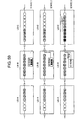
Fig. 3 illustrates a basic circuit diagram of
another embodiment of the identification number
generator circuit according to the present invention.
This embodiment takes into account to readily implement
a form which may utilize a type of cell that substantially
comprises a digital circuit or a logical
circuit. In this embodiment, logical threshold values
of the four CMOS inverter circuits INV1 to INV4 are
combined two by two for comparison by the comparator
COMP. The logical threshold values of these CMOS
inverter circuits INV1 to INV4 are compared in round
robin (league tournament).
-
Fig. 4 is a diagram for describing the
operation of the identification number generator
circuit in Fig. 3, showing an exemplary result of the
round robin comparison. Figs. 4(A) and (B) are, so to
speak, match tables indicating to make on-state every
one of switches Y1 to Y2 and switches X1 to X4, wherein
a symbol "+" is written into the figure when a positive
(high level) result is presented by subtracting the
potential at a short-circuited node of a CMOS inverter
circuit selected by a switch (X) connected to a non-inverting
input terminal (-) of the comparator COMP
from the potential at a short-circuited node of the
CMOS inverter circuit (i.e., the logical threshold
value voltage) selected by a switch (Y) connected to a
non-inverting input terminal (+) of the comparator
COMP, while a symbol "-" is written when a negative
(low level) result is presented. "*" indicates a self
match (no match) and therefore is invalid.
-
Referring to Fig. 4(A), Y1 has three "+",
i.e., a clean score. Then, Y2 has two "+"; Y3 has one;
and Y4 has zero (complete defeat). Specifically, since
the logical threshold values (VLT) of the CMOS inverter
circuits can be determined in magnitude with the number
of "+," they are in the order of VLT1 (logical
threshold value of INV1) - VLT2 - VLT3 - VLT4.
-
Fig. 4(B) shows another example. It is
assumed herein that apparent differences exist among
the logical threshold values of the respective CMOS
inverter circuits. Specifically, actual games and the
like involve draw matches and competitors having the
same number of wins. A draw match is represented by
(=). When there is such a draw match (=), Y1 and Y2
are at the same rank, while Y3 and Y4 are also at the
same rank, failing to establish the order as mentioned
above. Also, while the comparison (game) is made 16
times in this embodiment, the minimum number of games
with n teams in round robin is n(n-1)/2 with suffice,
so that six times may be actually sufficient.
-
The embodiment of Fig. 3 is composed of one
comparator and two selector circuits in a relatively
simple configuration as compared with the embodiments
of Figs. 1 and 2. However, since the identification
number generator circuit employs the comparator COMP
which is an analog circuit, it may encounter
difficulties in the formation in a semiconductor
integrated circuit device such as a gate array and
logic ASIC.
-
Fig. 5 illustrates a basic circuit diagram of
another embodiment of the identification number
generator circuit according to the present invention.
This embodiment does not employ any analog circuit as
in the embodiments of Figs. 1 to 3, but represents a
basic circuit composed only of a CMOS logic circuit and
a MOSFET switch.
-
All the CMOS inverter circuits INV1 to INV4
in Fig. 5 have the same size. Each of the CMOS
inverter circuits INV1 to INV3 is provided with four
switches. Switches A (A1 to A4) and B (B1 to B4) are
simultaneously opened and closed in association with
each other. Likewise, switches C (C1 to C4) and D (D1
to D4) are also opened and closed in association with
each other.
-
Fig. 6 illustrates an equivalent circuit
corresponding to open/close states of the switches for
describing the circuit in the embodiment of Fig. 5. In
Fig. 5, switches A1, B1, C2, D2 are closed (on-state).
The switch B1 short-circuits the input/output of the
CMOS inverter circuit INV1, and the voltage at the
short-circuited node is supplied to a common node P
through the switch A1. A potential at the common node
P is applied to the input of the CMOS inverter circuit
INV2 through the switch C2, and the output of the CMOS
inverter circuit INV2 is supplied to a common node PP
through the switch D2. Amplifier circuits AMP1 and
AMP2 are configured of CMOS inverter circuits which are
congruent in shape with INV1 to INV4.
-
In the equivalent circuit of Fig. 6, the
input and output of the CMOS inverter circuit INV1 are
short-circuited by the switch B1 which is turned on,
and the potential at the common node P is equal to the
logical threshold value of the CMOS inverter circuit
INV1 by the action of the switch A1 which is turned on.
The input to the CMOS inverter circuit INV2 is
connected to the common node P through the switch C2
which is turned on. If the CMOS inverter circuits INV1
and INV2 have completely the same electrical
characteristics, the potential at the common node PP
connected to the output of the CMOS inverter circuit
INV2 is qual to that at the common node P. Similarly,
the amplifier circuits AMP1 and AMP2 also have the same
potential at output nodes. In other words, the
input/outputs of the four inverters are all equal to
the logical threshold value voltage of the CMOS
inverter circuit INV1. However, this is an ideal
condition, and in an actual semiconductor device,
slight differences in the characteristics result in
different potentials at the respective nodes.
-
For example, when the logical threshold value
VLT1 of the CMOS inverter circuit INV1 and the logical
threshold value VLT2 of the CMOS inverter circuit INV2
are in a relationship represented by VLT1<VLT2, the
potential at the common node PP is higher than the
potential at the common node P. Conversely, when
VLT1>VLT2, the potential at the common node PP is lower
than the potential at the common node P.
-
The CMOS inverter circuit, which is a high
gain inverting amplifier, has a gain which varies
depending on the operation point. A maximum gain is
provided when an input potential is near the logical
threshold value of the CMOS inverter circuit.
Generally, the CMOS inverter circuit has an inverting
gain in a range of several tens to one hundred times
near the logical threshold value thereof.
-
Therefore, the difference between the logical
threshold values of the CMOS inverter circuits INV1 and
INV2 in Fig. 6 is amplified by the CMOS inverter
circuit INV2 at the later stage. Specifically, the
logical threshold value voltage generated by the former
CMOS inverter circuit is compared in magnitude with the
logical threshold value voltage of the later CMOS
inverter circuit itself, as a reference voltage, and
amplified.
-
The amplification is also made by the
amplifier circuits AMP2, AMP3, so that the difference
between the logical threshold values of the CMOS
inverter circuits INV1 and INV2 is amplified by a
factor of several tens of thousands of times by the
CMOS inverter INV2 and amplifier circuits AMP1, AMP2.
Finally, a CMOS supply voltage amplitude signal can be
generated at a node Q. Specifically, the result of a
comparison of magnitude between the logical threshold
values of the two CMOS inverter circuits INV1 and INV2
(a positive or negative sign) can be detected by the
CMOS amplitude signal.
-
By changing a combination of opened and
closed switches as in Fig. 6, all the CMOS inverter
circuits INV1 to INV4 can be readily compared to
provide the result as shown in Fig. 4(A). In this way,
the circuit in this embodiment is suitable for a
comparison of logical threshold values of CMOS inverter
circuits.
-
Specifically, with a combination of CMOS
inverter circuits and switches, a single CMOS inverter
circuit can be used as a source of the logical
threshold value voltage, or can be used as a determination
circuit for determining a logical threshold value
voltage generated by another CMOS inverter circuit, so
that an extra comparator is not required, making it
possible to significantly simplify the circuit
configuration. Moreover, since the entirety, including
the CMOS inverter circuits, is built by MOSFETs which
perform switching operations, no particular
difficulties will be experienced when mounted in a
semiconductor integrated circuit device such as a gate
array and a logic ASIC.
-
Fig. 7 illustrates a circuit diagram of a
specific embodiment corresponding to the embodiment of
Fig. 5. The CMOS inverter circuits INV1 to INV4 and
amplifier circuits AMP1, AMP2 are CMOS inverter
circuits in congruent shape. In this embodiment, N-channel
MOSFETs are used as the aforementioned
switches. Then, a binary counter and a decoder are
provided for forming control signals Y1 to Y4 and X1 to
X4 for these switches.
-
The CMOS inverter circuit INV1 is taken as an
example in the following description. The control
signal X1 is supplied to the gate of a switch MOSFET
which short-circuits the input and output of the CMOS
inverter circuit INV1, and a switch MOSFET which
connects the common node P to the input. The control
signal Y1 is supplied to the gate of a switch MOSFET
which connects the input of the CMOS inverter circuit
INV1 to the common node P and a switch MOSFET which
connects the output to the common node PP. Likewise,
in the respective CMOS inverter circuits INV2 to INV4,
the control signals X2 to X4 and control signals Y2 to
Y4 are connected to the gates of the corresponding
switch MOSFETs, respectively.
-
The binary counter is a binary counter having
a total of four bits, which is reset by a reset signal
RES and counts the number of pulses in a clock signal
CLK supplied thereto. The decoder forms the control
signals Y1 to Y4 corresponds to the lower two bits of a
count output, and forms the control signals X1 to X4
corresponding to the higher two bits of the count
output.
-
Fig. 8 shows a timing chart for describing
the operation of the circuit in the embodiment of Fig.
7. The reset signal RES is for initializing the binary
counter. Here, the output of the binary counter is all
"1" during a reset (RES="H") and immediately after the
reset. Therefore, X4 and Y4 are active in the output
of the decoder. The binary counter advances (+1) at
the time the clock CLK first rises after the reset is
released, so that the output changes to all "0."
Therefore, the control signals X1 and Y1 are active in
the output of the decoder.
-
Subsequently, the output of the binary
counter repeatedly advances (+1) at the timing at which
the clock signal CLK rises, causing the decoder to
advance as shown in Fig. 8. Of course, it goes without
saying that the output of the binary counter again
returns to all "0" when the clock signal CLK rises 17
times. However, since necessary information can be
retrieved up to 16 operations in this embodiment, the
clock operations are not needed at the 17th time
onward.
-
After the reset is released, the binary
counter advances its counting operation each time the
clock signal CLK rises, and information b1 to b16
delivered at an output node OUT each time is as shown
in Fig. 9. As described above, the difference between
the logical threshold values of the CMOS inverter
circuits is amplified by the amplifier circuits AMP1,
AMP2, and "H" (high level) is outputted at the output
terminal when VLTQy-VLTQx>0, and "L" (low level) is
outputted at the output terminal OUT when VLTQy-VLTQx<0.
-
Thus, the results of matches in round robin
among the four CMOS inverter circuits INV1 to INV4 can
be utilized as they are as the identification signals
b1 to b16. Among the results b1 to b16 in the round
robin of the four CMOS inverter circuits INV1 to INV4,
those of self matches may be previously set to a
particular level, high level or low level, as later
described. Numbers 1 to 4 assigned to the four CMOS
inverter circuits are replaced with 2-bit information
pieces which can be arranged in the descending order,
for example, as 1-2-3-4, so that resulting identification
information can be compressed to one half, as
2x4=8 bits.
-
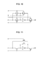
Fig. 10 illustrates an exemplary modification
of one embodiment of a unit circuit which comprises a
CMOS inverter circuit and switch MOSFETs that are the
core of the identification number generator circuit
according to the present invention. In the circuit of
Fig. 10, each of the four switch MOSFETs (A to D) in
Fig. 5 is composed of a CMOS pair. Specifically, an N-channel
MOSFET and a P-channel MOSFET are connected in
parallel, and complimentary signals X and X/ are
supplied to their gates, respectively.
-
When the CMOS switches are used in this
manner, a voltage signal transmitted through the switch
MOSFETs is not limited by the threshold value voltages,
so that this is effective for a circuit which operates
at a low voltage, wherein a voltage difference between
a supply voltage or a ground potential of the circuit
and the logical threshold value voltage, or a
differential voltage between the supply voltage or the
ground potential of the circuit and a voltage to be
outputted to the common node PP is smaller than the
threshold value voltage of the switch MOSFET.
-
Fig. 11 illustrates an exemplary modification
of another embodiment of the unit circuit which
comprises a CMOS inverter circuit and switch MOSFETs
which are the core of the identification number
generator circuit according to the present invention.
The circuit in Fig. 11 changes the position of the N-channel
switch MOSFET which supplies the common node P
with the input/output short-circuit potential of the
CMOS inverter circuit. In other words, the output side
of the CMOS inverter circuit, which is short-circuited
between the input and output, is connected to the
common node P.
-
Fig. 12 illustrates an exemplary modification
of another embodiment of the unit circuit which
comprises a CMOS inverter circuit and switch MOSFETs
which are the core of the identification number
generator circuit according to the present invention.
The circuit of Fig. 12 comprises two P-channel MOSFETs
which are connected in series between the input of the
CMOS inverter circuit and a supply voltage terminal.
These P-channel MOSFETs are supplied with selection
signals X, Y at the gates, respectively. In this
embodiment, when the CMOS inverter circuit is not
selected, i.e., when neither the selection signal X nor
Y is activated, the P-channel MOSFET is turned on to
clamp the input of the CMOS inverter circuit at a high
level such as a supply voltage to prevent a through
current in the CMOS inverter circuit. Specifically,
when the input of the CMOS inverter circuit is
floating, a resulting intermediate potential can cause
a large through current to flow between the N-channel
MOSFET and P-channel MOSFET of the CMOS inverter
circuit. Thus, the P-channel MOSFETs are provided to
prevent the through current.
-
Fig. 13 illustrates exemplary modification of
another embodiment of the unit circuit which comprises
a CMOS inverter circuit and switch MOSFETs which are
the core of the identification number generator circuit
according to the present invention. In the circuit of
Fig. 13, the switch MOSFETs are changed from the N-channel
MOSFETs as in the foregoing embodiment to P-channel
MOSFETs, and the input of the CMOS inverter
circuit is clamped to a low level by an N-channel
MOSFET when it is placed in an inactive state. In this
event, selection signals applied to the gates of the N-channel
MOSFETs are inverted signals X/ and Y/.
-
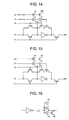
Fig. 14 illustrates an exemplary modification
illustrating another embodiment of the unit circuit
which comprises a CMOS inverter circuit and switch
MOSFETs which are the core of the identification number
generator circuit according to the present invention.
The circuit of Fig. 14 comprises two N-channel MOSFETs
connected in series between the input of the CMOS
inverter circuit and the ground potential of the
circuit for preventing the common node PP from being
indefinite at the aforementioned self match (no match),
i.e., the output from being instable whether it becomes
"H" or "L," and the input of the CMOS inverter circuit
is clamped to a low level.
-
These N-channel MOSFETs are supplied with
selection signals X and Y at the gates, respectively.
In this way, the selection signals X, Y are at high
level during a self match, and the input is supplied
with the ground potential of the circuit. A short-circuit
switch provided between the input and output of
the CMOS inverter circuit is comprised of a series
circuit of an N-channel MOSFET which receives the
selection signal X and a P-channel MOSFET which
receives the selection signal Y. In this way, the
input and output are not short-circuited during a self
match, and a high level can be outputted corresponding
to the clamped low level supplied to the input. Also,
the input is clamped to a high level such as a supply
voltage, as is the case with the embodiment of Fig. 12,
upon non-selection.
-
Fig. 15 illustrates an exemplary modification
illustrating another embodiment of the unit circuit
which comprises a CMOS inverter circuit and switch
MOSFETs which are the core of the identification number
generator circuit according to the present invention.
In the circuit of Fig. 15, the input of the CMOS
inverter circuit is clamped to a high level for
preventing the common node PP from being indefinite at
the aforementioned self match (no match), i.e., the
output from being instable whether it becomes "H" or
"L," and the input of the CMOS inverter circuit is
clamped to a low level. In a manner similar to the
foregoing, for preventing short-circuit between the
input and output during the self match, the short-circuit
switch is comprised of a series circuit of an
N-channel MOSFET and a P-channel MOSFET, as is the case
with the embodiment of Fig. 14.
-
The object and effect of avoiding an
indefinite level at the common node PP will be
described later in detail. The respective exemplary
modifications illustrated in Figs. 10 to 15 may be
implemented in combination. For example, the N-channel
switch MOSFETs in Fig. 14 may be replaced with a CMOS
pair.
-
In the embodiments of Figs. 14 and 15, the
self match (*) fields in Fig. 9 can be utilized to
embed fixed information. Inherently, the self match
field is indefinite, strictly speaking, this is the
result of a comparison between the logical threshold
values of each CMOS inverter circuit and amplifier
circuit AMP, so that the identification ability will
not be degraded even if information in this field is
ignored or used for a different purpose. When the
added N-channel MOSFETs in series connection are
clamped to the ground potential or supply voltage as in
Figs. 14 and 15, the inputs of the CMOS inverter
circuits INV1 - INV4 can be biased to a low level or a
high level side to arbitrarily set the output for the
self match field.
-
In recent years, the semiconductor integrated
circuit device technology is under progress for
mounting bare chips on a substrate referred to as a
build-up substrate, wherein either a product or a
shipment date cannot be identified from the appearance,
so that there is an increasingly high need for
inserting a unique number for identifying the product
or shipment date. Specifically, in System On Chip
(SOC) as later described, individual product management
becomes increasingly important, as to what is mounted
on a base chip, which types of individual chips are
combined, which chips should be combined, and the like.
Therefore, the assignment of the unique number is
advantageous.
-
Fig. 16 illustrates a circuit diagram
illustrating one embodiment of a CMOS inverter circuit
used in the identification number generator circuit
according to the present invention. Generally, a CMOS
inverter circuit comprises a P-channel MOSFET and an N-channel
MOSFET arranged in series between a supply
voltage and a ground potential of the circuit, their
gates are connected in common for use as an input, and
their drains are connected in common for use as an
output. The CMOS inverter circuits INV1 to INV4 and
amplifier circuits AMP1, AMP2 in the aforementioned
embodiments can be each comprised of two MOSFETs as
described above.
-
In contrast, in this embodiment, a CMOS
inverter circuit is comprised of two P-channel MOSFETs
and two N-channel MOSFETs. The two N-channel MOSFETs
are connected in parallel between an output terminal
and a ground potential point of the circuit, while the
two P-channel MOSFETs are connected in series between
the supply voltage and output terminal.
-
In this configuration, the N-channel MOSFETs
have large conductance, whereas P-channel MOSFETs have
small conductance. Specifically, a current flowing
into the N-channel MOSFETs is set by the small
conductance (large on-resistance) of the P-channel
MOSFETs. Apparently, since a constant voltage can flow
into the N-channel MOSFETs, the threshold value
voltages of the two N-channel MOSFETs predominantly act
on the logical threshold voltage of the CMOS inverter.
In this way, the logical threshold value of the CMOS
inverter circuit is less prone to the influence of
fluctuations in the supply voltage.
-
With the P-channel MOSFETs operated as simple
high resistance elements and the N-channel MOSFETS
having the threshold value voltages predominantly
acting on the logical threshold value, the resulting
configuration is advantageously less prone to the
influence of deteriorated element characteristics
(NBTI), later described.
-
As will be later described, when an identification
number generator circuit is comprised of a gate
array, N-channel MOSFETs and P-channel MOSFETs have
fixed element sizes, so that a plurality of MOSFETs may
be combined as mentioned above to equivalently provide
a different ratio of the element size of an N-channel
MOSFET to the element size of a P-channel MOSFET to set
a logical threshold value corresponding thereto.
-
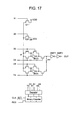
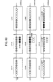
Fig. 17 illustrates a circuit diagram of
another embodiment of the identification number
generator circuit according to the present invention.
This embodiment illustrates a circuit for fixing a
portion of an identification number to an arbitrary
number in addition to the function so far described for
generating a random identification number. In the
embodiment illustrated in Fig. 7, 24 different
identification numbers can be generated. The number of
information bits are 16 bits including the self match
result. Briefly describing the circuit in this
embodiment, the output node (common node) P of the CMOS
inverter circuit shown at the first stage in the
aforementioned Fig. 6 is forcedly fixed to an arbitrary
value. In this event, the first stage and second stage
cannot be changed in the order.
-
In the circuit of this embodiment, from the
circuit in the embodiment of Fig. 7, an output node
corresponding to the CMOS inverter circuit INV1 is
clamped to "H" (=VDD) by MOSFET Q11, and an output node
corresponding to the CMOS inverter circuit INV2 is
clamped to "L" (=VSS) by MOSFET Q21. Since the MOSFETs
Q11 and Q12 for forming the thus clamped levels "H" and
"L" are not inputs to the common node P, decode signals
Y1 and Y2 are not needed. For this reason, the binary
counter circuit is provided in a three-bit configuration,
and the decoder circuit forms output signals as
Y3, Y4.
-
Fig. 18 illustrates a waveform chart for
describing the operation of the circuit in the
embodiment illustrated in Fig. 17. There are four
options at the first stage and two options at the
second stage, so that a total of eight different
outputs can be provided. In other words, the number of
information bits are eight bits. In this embodiment,
output signals b1 to b4 present "0," "0," "1," "1" at
all times. The remaining b5 to 58 represent the result
due to variations in logical threshold values of CMOS
inverter circuits Q3 and Q4. This embodiment can
generate only two different fixed numbers and two
different random identification numbers at maximum.
-
In actual use, the fixed section and random
section can be a combination of arbitrary sizes. A
possible application may be such that the fixed section
indicates a product code, and the random section
indicates a sample number. A fixed identification
number may be inserted into an information bit sequence
in several other methods. For example, there are the
method of replacing the self match field, the method of
replacing one of repeated matches (comparison of
changed first and second stages), as described in
connection with Figs. 14, 15. For actually implementing
these circuits, a problem arises in that which part
of a registration and matching system is burdened with
the function, not only the circuit for generating
identification numbers. However, in the overall
system, the registration and matching functions are
likely to be mainly implemented by computer software,
so that advanced functions can be relatively readily
implemented.
-
Fig. 19 illustrates a block diagram
illustrating another embodiment of the identification
number generator circuit according to the present
invention. A logical threshold value determination
unit, substantially represented by blocks in Fig. 19,
is operated by a voltage V2, which is relatively low
and stabilized, outputted from a power supply circuit
shown in Fig. 19 and next described.
-
Specifically, a P-channel MOSFET applied with
a ground potential of the circuit at its gate at all
time operates as a loading means to supply an operating
current to four N-channel MOSFETs serially connected in
diode configuration which act as voltage regulator
elements. In this way, a constant voltage V1 is formed
corresponding to a constant voltage (threshold value
voltage) between the gate and source of the N-channel
MOSFETs in series connection, and is supplied as an
operating current V2 for the logical threshold value
determination unit through the gate and source of the
N-channel MOSFET. The voltage supplied to such a
logical threshold value voltage determination unit is
made constant. As a result, the logical threshold
values of the CMOS inverter circuits INV1 to INV4 and
the like are less affected by fluctuations in the
supply voltage VDD. In this way, a more stable
operation can be expected for determining the logical
threshold value.
-
In the invention of this application, it is
not essential to provide a constant operating voltage
to the logical threshold value determination unit as
described above. Specifically, the invention of this
application does not employ the absolute values of the
logical threshold value voltages of a plurality of CMOS
inverter circuits, but sets an identification number
corresponding to a difference between the logical
threshold value voltages of the individual CMOS
circuits. Since the fluctuations in the supply voltage
similarly affects the logical threshold value voltages
of the respective CMOS inverter circuits, the relation
of magnitude will not be significantly changed.
-
Fig. 19(B) illustrates a specific circuit for
preventing aging changes of MOSFET. The threshold
value voltage of a MOS transistor may undesirably
fluctuate due to an electric field stress which depends
on an electric field strength and temperature.
Particularly, a phenomenon referred to as NBTI
(Negative Bias Temperature Instability) remarkably
appears in P-channel MOSFET. Often used as countermeasures
to this is a method of applying a high voltage
to the gate of the PMOS out of an intended time. In
this embodiment, the ground potential VSS of the
circuit of the logical threshold value determination
unit is supplied from the N-channel MOSFET, and the N-channel
MOSFET is turned on by a power supply control
signal PON at high level in a logical threshold value
determining operation to supply the ground potential
VSS of the circuit. Then, except for the logical
threshold value determining operation, the power supply
control signal PON is brought to low level to turn off
the N-channel MOSFET and to turn on the P-channel
MOSFET to supply the supply voltage VDD to the ground
potential side of the circuit as well. Then, the P-channel
MOSFET is applied with a fixed gate voltage at
the gate to supply the supply voltage VDD. In this
way, the P-channel MOSFET is equi-potential, equal to
the supply voltage VDD, at all of the gate, drain,
source and substrate (channel), thereby minimizing
fluctuations in the logical threshold value due to
aging changes of the MOSFETs.
-
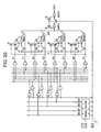
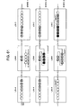
Fig. 20 illustrates a circuit diagram of
another embodiment of the identification number
generator circuit according to the present invention.
In the circuit of this embodiment, a series circuit of
P-channel MOSFET is provided at the input of each CMOS
inverter circuit INV1 to INVV4 to minimize fluctuations
in the logical threshold value due to aging changes of
the MOSFETs. At a reset, at which a signal RES/ is set
to low level, the inputs of the CMOS inverter circuits
INV1 to INV4 are clamped to the supply voltage.
-
Specifically, with the signal RES/ at low
level (logical zero), output signals of AND gate
circuits, which receive count outputs B0 to B3 of a
binary counter circuit, are all set to high level
(logical one). As a result, all of output signals Y1
to Y4 and X1 to X4 of NOR gate circuits, which form
parts of a decoder circuit, transition to low level
(logical zero), causing the P-channel MOSFETs in series
connection arranged between the inputs of the respective
CMOS inverter circuits INV1 to INV4 and the supply
voltage VDD to turn on, thereby clamping them to the
supply voltage. In this way, the supply voltage VDD is
supplied to the gates of the P-channel MOSFETs which
form parts of the respective CMOS inverter circuits
INV1 to INV4.
-
Further, in this embodiment, the P-channel
MOSFET, which is turned on by the signal RES/ at low
level, clamps the inputs of the amplifier circuits AMP1
and AMP2 to the supply voltage VDD, to supply the
voltage voltage to the gates of P-channel MOSFETs which
form parts of the amplifier circuits.
-
Alternatively, the selection signals Y1 to Y4
may be all turned on to clamp the common input node P
to the supply voltage. In any case, an action may be
taken to control the gate voltages of the P-channel
MOSFETs which form parts of the CMOS inverter circuits
INV1 to INV4 and amplifier circuits AMP1, AMP2 in this
manner, or to fully shut off the power supply to the
identification number generator circuit. However, in
the method of fully shutting off the power supply, it
is necessary to take into consideration the electric
separation of the element regions, in which the MOSFETs
that form parts of the identification number generator
circuit are formed, from other circuits. Specifically,
this is because, even if the power supply is shut off,
a constant voltage always applied to the substrate gate
(channel) of MOSFET is not desirable from view point of
the degradation in the element characteristics.
-
On the other hand, when attention is paid to
such NBTI, a problem arises in a normal reliability
guarantee. Specifically, the provision of a means for
circumventing a stress as mentioned above disables
screening of process defects which is performed in a
so-called burn-in step. While there is no concern if
the scale of the circuit is extremely smaller than the
entire LSI, it should be advisable to bear in mind
those applications which need the screening. In this
event, a mode is provided for arbitrarily releasing a
reset or a power-off in the burn-in step or the like.
-
Of course, it is well contemplated that the
stress causes an identification number to fluctuate.
However, a final identification number can be retrieved
after the burn-in step for re-registration in a database,
and even large fluctuations in the identification
number exert small influence because lots treated in
the burn-in step are limited in size in a range of
several hundreds to several thousands.
-
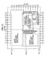
Fig. 21 illustrates a general block diagram
of one embodiment of a semiconductor integrated circuit
device according to the present invention. This
embodiment is directed to a power control for a system
LSI which is mounted with the identification number
generator circuit of this application. This system LSI
employs two different types of power supplies VDD1 and
VDD2 by way of example.
-
The identification number generator circuit
receives the power supply from VDD1 in operation.
Here, "in operation" refers to a time period for which
an identification number is sent out in response to an
identification number read request from the LSI circuit
main unit 1. In other states, the power supply is shut
off. A signal for controlling the power supply is a
power supply control signal which is applied to a power
supply control circuit. The power supply control
circuit is composed of an N-channel MOSFET and a P-channel
MOSFET which receive the power supply control
signal at the gate. When the power supply control
signal is at high level, the power supply of the
identification number generator circuit is clamped to
VSS, and an identification number output signal is
clamped at low level. When the power supply control
signal is at low level, the identification number
generator circuit is supplied with VDD1. Circuits
included in the illustrated identification number
generator circuit are, for example, the logical
threshold value determination circuit for CMOS inverter
circuits, binary counter, and decoder, which are shown
in Fig. 20, wherein the binary counter and decoder may
be included in the LSI circuit main unit 1.
-
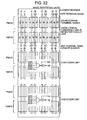
Fig. 22 illustrates an element layout diagram
of elements in one embodiment which is suitable for the
semiconductor integrated circuit device according to
the present invention. Though the illustrated
configuration is not particularly limited, the layout
may be understood to be an example suitable for a so-called
master-slice semiconductor integrated circuit
device. For the ease of understanding, Fig. 22 only
illustrates a plane pattern of active regions which
comprise MOS transistors, and a wiring layer pattern
such as metal wiring layers are omitted from the
illustration. The essence of the technique will be
well understood from the fact that even such a plane
pattern predominantly affects the circuit characteristics
which should be provided in the MOS transistors,
but less affects the circuit characteristics which
should be provided in wires such as metal wires.
-
The basic device structure itself of the
semiconductor integrated circuit device is not directly
related to the present invention, so that detailed
description thereon is not made. However, this may be
generally described as follows.
-
Specifically, a semiconductor device used
herein is made of N-type single crystal silicon, and an
N-type well region and a P-type well region are formed
on the surface of the semiconductor substrate by a
localized impurity introduction technique. An opening
is formed for defining an active region in a so-called
field insulating film which may be made of a silicon
oxide film, disposed on the surface of the
semiconductor substrate, and a gate insulating film is
formed on the surface of the N-type well region and P-type
well region, which are exposed through the
opening, by a silicon thermal oxidization method or the
like. A gate electrode layer, which may be made of a
polycrystalline silicon layer, is selected on the gate
insulating film and field insulating film. A P-type
impurity is introduced using the gate electrode layer
and field insulating film as substantial impurity
introducing masks to form P-type semiconductor regions
on the surface of the N-type well region for providing
a source region and a drain region of a P-channel MOS
transistor. Similarly, an N-type impurity is
introduced using the gate electrode layer and field
insulating film as substantial impurity introducing
masks in a similar manner to form N-type semiconductor
regions on the surface of the P-type well region for
providing a source region and a drain region of an N-channel
MOS transistor. This basic device structure is
formed with desired wiring layers by known wiring layer
forming technique and insulating layer forming
technique.
-
In Fig. 22, a relatively small substantially
square pattern defines an active region. One unit
region is made up of the relatively small substantially
square pattern and two elongated patterns in parallel
with each other which are drawn to overlap the square
pattern to mean gate electrode layers, respectively.
For example, a unit region is made up of a relatively
small square pattern positioned at an upper right end
of the drawing and labeled with symbols PP, B, P, and
two elongated patterns which are drawn to overlap the
square pattern and labeled with symbols Y0/, X0/,
respectively.
-
Thus, one active region is formed with two
MOS transistors by two parallel gate electrode layers,
and semiconductor regions for the source and drain
formed on the surface of the active region in self
alignment to the two gate electrodes.
-
In Fig. 22, a plurality of unit regions for
N-channel MOS transistors, and a plurality of unit
regions for P-channel MOS transistors are arranged in
columns as illustrated. In the column comprised of
four unit regions for P-channel MOS transistors,
located at the highest position (hereinafter referred
to as the "first region column"), the respective unit
regions are configured to have the same plane
dimensions and the same extension direction as one
another. Likewise, the respective unit regions in the
column comprised of four unit regions for N-channel MOS
transistors located immediately below the first column
are configured to have the same plane dimensions and
the same extension direction as one another. The first
region column and second region column are provided to
create an inverter and a switch MOS transistor
connected thereto as in Fig. 20.
-
Similarly, a third region column and a fourth
region column are provided to create an X-decoder unit,
while a fifth region column and a sixth region column
are provided to create a Y-decoder unit.
-
The entirety of the first region column to
sixth region column in Fig. 22, each of which is
comprised of four unit regions, is designated as a
basic repetition unit. Specifically, a plurality of
basic repetition units in Fig. 22 are arranged side by
side in the lateral direction in Fig. 22 in accordance
with a circuit scale to be achieved. According to this
configuration, the first region columns in different
basic repetition units also constitute a single column
(also referred to as the "global region column") in the
entire layout. Similarly, the second columns and
onward constitute global region columns, respectively.
-
The layout in Fig. 22 and the repeated layout
as mentioned above provide an example suitable for
forming identification information of the present
invention.
-
Instead of the layout in Fig. 22, if a
plurality of unit regions which should make up the same
region column are disposed across element regions or
the like which make up other circuits and therefore are
spaced by a relatively large distance from one another,
the following difficulties may arise. Specifically, a
plurality of unit regions significantly suffer from the
influence exerted by macroscopic fluctuations in
pattern dimensions as based on fluctuations in
manufacturing conditions of the semiconductor
integrated circuit device, or macroscopic fluctuations
such as distorted patterns, resulting in a relatively
large difference in pattern shape.
-
Since a mechanical stress applied to a
semiconductor chip by mounting the semiconductor chip
can differ from one site to another of the semiconductor
chip, a plurality of unit regions can be applied
with mechanical stresses which relatively largely
differ from one unit region to another. A rise in
operating temperature caused by a power supply current
flowing through the circuit is not uniform in the
plurality of unit regions. The thickness of the gate
insulating film and a subtle change in the
concentration of introduced impurities can be
relatively increased due to the plurality of unit
regions which are relatively distanced from one
another.
-
In the layout of Fig. 22, a plurality of unit
regions belonging to the same region column are
disposed in relatively close proximity, and have the
same size and the same direction as one another, so
that they are less susceptible to the influence exerted
by relative pattern dimensions, distorted patterns,
mechanical stress, operating temperature, film
thickness, and impurity concentrations, as mentioned
above.
-
A so-called phase shift mask technique is
understood to be an effective technique for
miniaturizing circuit components, wires and the like,
which make up a semiconductor integrated circuit
device, to a so-called sub-micron level. In such a
phase shift mask technique, a pattern can suffer from
asymmetry or distortions such as a difference in shape
in the left and right halves of a pattern to be formed,
due to even a slight change in phase difference of
light for exposing a photosensitive material layer
which is later used as a mask. The layout as in Fig.
22 can sufficiently reduce deviated electric
characteristics of a plurality of unit regions even if
such a type of distorted pattern is present.
-
The influence exerted by the crystal
orientation dependance of the carrier mobility in the
semiconductor, together with the difference in
configuration in the foregoing point of view, cannot be
treated lightly for the present invention which
utilizes the microscopic characteristics as mentioned
above. In the layout of Fig. 22, the MOS transistors
belonging to the first region column and the MOS
transistors belonging to the second region column are
free from the difference in the characteristics due to
the crystal orientation dependency because all of a
plurality of gate electrode layers forming part of the
first region column are made in the same orientation
and in the same pattern as one another, and all of a
plurality of gate electrode layers forming part of the
second region column are also made in the same
orientation and in the same pattern as one another.
-
It will be understood from the foregoing that
the layout of Fig. 22 is made in consideration of a
significant reduction in the macroscopic variations or
deviations in characteristics as mentioned above from
the viewpoint of designing and manufacturing of the
semiconductor integrated circuit device and in
consideration of appropriate utilization of the
microscopic variations as mentioned above.
-
When a need exists for more fully eliminating
the deviations in electric characteristics of the MOS
transistors created in the layout of Fig. 22, a dummy
region can be set for solving an end effect of the
overall array comprised of a plurality of the basic
repetition units of Fig. 22. The dummy region is
provided to make the ends of the overall array
comparable to the interior of the overall array on the
layout, and is comprised of at least a plurality of
unit regions at the ends in the basic repetition units.
-
When this type of dummy region is not set, a
machined shape of such ends can be affected depending
on the configuration outside the ends in the overall
array, and such ends and the remaining portions can be
applied in different manners with a force which can
affect the element characteristics, such as a stress
produced between the semiconductor substrate and the
insulating film on the surface thereof. They can be
factors of causing the deviations in the electric
characteristics. When the dummy region as mentioned
above is set, the factors of causing the deviations in
the electric characteristics are fully eliminated.
-
The dummy region can be provided as a region
which is not utilized as a circuit or as a region for
making other circuit which does not require attention
to the deviations in the electric characteristics.
-
Fig. 23 illustrates an equivalent circuit
diagram corresponding to the foregoing Fig. 22. In
Figs. 22 and 23, the terminal names and element numbers
are corresponding. However, details of the decoder
unit are not illustrated because there are no
particular restrictions except that it is disposed
below (or above) the CMOS logical threshold value
detector circuit. When the basic repetition units as
in Fig. 22 are disposed in parallel, CMOS inverter
circuits formed of elements can match the shape and
surrounding environment with the same circuits adjacent
thereto. In an layout scheme other than a gate array
scheme, the basic repetition units may be laid out such
that the CMOS inverter circuits are congruent. When
the circuit is built using such gate arrays, the
embodiment in Fig. 16 may be applied, in which case
variations in the threshold value voltage of the N-channel
MOSFET can be predominantly reflected to the
logical threshold value, while reducing the influence
of variations in the supply voltage.
-
Fig. 24 illustrates a block diagram of one
embodiment when the present invention is applied to a
dynamic RAM (random access memory, hereinafter simply
referred to as the "DRAM"). In this embodiment, the
binary counter and decoder are removed from the
identification number generator circuit illustrated in
Fig. 20 or the like. Instead of these counter and
decoder, a row address signal and a column address
signal of a DRAM, which is mounted with the same, are
supplied with the signals X and Y, formed by the
decoder, for direct use as a selection signal for the
logical threshold value determination circuit of the
CMOS inverter circuit. An identification number read
mode is set for the DRAM, a start signal is generated
by a circuit DFT, and address signals X and Y are
supplied from the outside for the read, to output an
identification number generated by the identification
number generator circuit through an input/output
circuit and a DQ pin, instead of a selection operation
of the memory array. In this event, since the address
signals X and Y can be input in an arbitrary order,
fixed information in the self match fields alone can be
specified for reading. Alternatively, the order in
which the address signals X and Y are inputted may be
entered as a code, such that a particular one can
output a fixed signal corresponding to the self match
or the identification number.
-
This configuration can be applied as well to
semiconductor integrated circuit devices other than
DRAM, such as other semiconductor memory devices such
as another static RAM, flash EPROM and the like or a
CPU (microprocessor) having address terminals, and the
like.
-
Fig. 25 illustrates general schematic diagram
of one embodiment of a semiconductor integrated circuit
device which employs the identification number
generator circuit according to the present invention.
The essential purpose of assigning an identification
number to a semiconductor integrated circuit device is
to give a unique number to each LSI. While a numbering
method may use a laser fuse, a flash (FLASH) memory or
the like, a special process or program step and the
like are required.
-
In this embodiment, an identification number
generated by the identification number generator
circuit of this application in a wafer state is read by
a tester for registration in relation to a variety of
data and the like in a workstation. After each LSI is
finished into a product and mounted in an electronic
device such as a personal computer PC and the like, the
identification number is read from the LSI. The
identification number read a this time is not ensured
to completely match because even the same LSI differs
in an operating environment and condition from the
registration time. However, it can be estimated to be
the same or not from the degree of discrepancy in
identification number.
-
Description will be made on a determination
algorithm for the identification system in this
application. The identification number in this
embodiment indicates the order of magnitude of the
logical threshold values of a plurality of CMOS
inverter circuits. A circuit having four CMOS inverter
circuits as in the foregoing embodiment is counted as
one unit. For example, there are 24 possible orders
(the number of permutations) 4P4=4!=4x3x2x1=24 for the
logical threshold values of the four CMOS inverter
circuits. Assuming now that there are two units, if
the logical threshold values completely randomly vary,
the two units of CMOS inverter circuits has the same
order with a probability of approximately 4.2 % (=1-23/24).
-
Otherwise, when one unit is comprised of
eight CMOS inverter circuits, there are 8!=40,320
possible orders. When there are 50 such units, one set
or more of those having the same order exist with a
probability of approximately 3 % (=1-(40320x40319x ...
x 40271) / 4032050).
-
In a unit comprised of 16 CMOS inverter
circuits, possible combinations amount to 16!=2.09E13.
As such, the permutations of 16 is an extraordinary
number, meaning that when the logical threshold values
of the CMOS inverter circuits randomly vary, there
hardly exist those which are in the same arrangement.
Actually, when there are 1,000,000 units, it is
estimated that one set or more of units in the same
order exist with a probability of at least 5 % or less
(at a rough estimate because a strict calculation is
difficult due to a large number of digits). In other
words, there is one set per 20,000,000 units when
roughly speaking. It is contemplated from such
calculations that approximately 16 CMOS inverter
circuits are required in one unit for completing a
practical identification number. Therefore, the
following description will be made on a unit comprised
of 16 CMOS inverters, given as an example.
-
When 16 CMOS inverter circuits in one unit
are implemented as in Fig. 7, round-robin comparison
results amount to 256 including self-matches. In the
following, one comparison result output is referred to
as "one bit."
-
Fig. 26 is the most simple example in which
the logical threshold values of 16 CMOS inverter
circuits are arranged in sequence as VLTQ1>VLTQ2> ...
>VLTQ16.
-
Fig. 27 is an example in which the logical
threshold values of CMOS inverter circuits are at
random. "1" indicates that the second CMOS inverter
circuit has a logical threshold value higher than that
of the first one, "0" indicates that the second CMOS
inverter circuit has a logical threshold value lower
than that of the first one, and "*" indicates a self-match
or indefinite. As can be seen in the two
examples, bit patterns at OUT of the circuits
corresponding to Figs. 26 and 27 change to inherent
patterns depending on how the logical threshold values
of the CMOS inverter circuits are ordered. Thus, a
direct use of the bit pattern at the output OUT as the
identification number can be deemed to be the most
simple manner. The number of bits of the identification
number information in this method, i.e., data
amount is 256 bits.
-
The bit pattern is nothing but a so-called
match result table itself. On the other hand, the
concept which underlies this application is the order
of magnitude of logical threshold values of a plurality
of CMOS inverter circuits. It is contemplated that the
data amount of information to be handled can be reduced
if information on the order of magnitude alone can be
retrieved from the match result table.
-
Figs. 26 and 27 show on the lower side and
right side total numbers of "1" or "0" in the vertical
direction and horizontal direction except for the self-match
fields. For example, looking at totals of "1" on
the lower sides of Figs. 26 and 27, the order of the
magnitude of number corresponds to the order of the
magnitude of the logical threshold value. Compared to
a league match of sports such as foot ball or baseball,
this is the same as a stronger team having a larger
number of wins. Speaking with the CMOS inverter
circuits, as a higher logical threshold value has a
larger number of "1."
-
Since the number of wins or the total number
of "1" is equivalent to the rank, the total number of
"1" can be used to represent the order of magnitude of
the logical threshold values of the CMOS inverter
circuits. Of course, no change is basically caused
even if the total number of "0" is used or a total
number of "1" or "0" in the horizontal direction is
used. With the use of this method, the data amount of
information bit can be reduced. Since each CMOS
inverter circuit can have an order which can be
represented by a number from 0 to 15, four bits of
information amount are required in binary notation.
Since there are 16 CMOS inverters, a total of 64 bits
(=4x16) are required. As compared with the foregoing
comparison result (match result) table, the data amount
can be reduced by a factor of four from 256 bits to 64
bits.
-
While one unit is herein comprised of 16 CMOS
inverter circuits, this effect is increased as the
number of CMOS inverter circuits is larger. For
example, with one unit comprised of 32 CMOS inverter
circuits, the comparison result table requires 1024
bits, whereas when the order is used, the number of
bits is reduced to 160 bits (5x32) by a factor of 6.5.
Stated another way, although the comparison results are
increased by a factor of four (=1024/256), this can be
reduced to an increase by a factor of 2.5 (=160/64)
with the order-based information. This is advantageous
in that the identification system manages a less amount
of data, and a processing time spent for matching can
be reduced.
-
Figs. 28 and 29 each illustrate a schematic
diagram of one embodiment of a matching algorithm in
the identification system for the semiconductor
integrated circuit device according to the present
invention. While description is herein made on a
method using comparison result information of the
logical threshold values of CMOS inverter circuits, a
method using the order of magnitude of logical
threshold values is identical in general flow.
-
Fig. 28 illustrates a registration method.
- (1) 256-bit comparison result information
for the logical threshold values of the CMOS inverter
circuits is read from the identification number
generator circuit.
- (2) The comparison result information is
registered in an identification number management
ledger and assigned a management number for relating to
a database which stores information such as measurement
data and the like.
- (3) The number of registrations is
incremented by one. While it is herein assumed that a
newly registered identification number is not the same
as those previously registered at all times, it is
effective to add a procedure for confirming a duplication
of registered one and generating some alarm upon
new registration.
-
-
Fig. 29 illustrates a matching method. This
system is characterized by allowing fluctuations in
identification number due to a difference in environment
and conditions between a registration instance and
a matching instance.
- (1) 256-bit comparison result information
for the logical threshold values of the CMOS inverter
circuits is read from the identification number
generator circuit.
- (2) Registered identification numbers are
sequentially retrieved from the management ledger.
- (3) The registered identification numbers
are compared with an identified number. A comparison
method will be later described.
- (4) The one having the smallest difference
between a registered identification number and the
identified number is selected as a matching candidate.
By repeating (2) to (4), the one finally having the
smallest difference of all the registered identification
numbers is selected as the most probable identical
candidate.
-
-
Fig. 30 illustrates an explanatory diagram
for an exemplary comparison method in Fig. 29. The
identified number is shown by extracting 24 bits or a
portion of the 256-bit comparison result output of the
logical threshold values of the CMOS inverter circuits.
Identification numbers 1 to 5 are registered identification
numbers. Shaded portions in them are portions
different from the bits of the identified number. A
total number of unmatch bits is shown at the right end.
-
As described in connection with Fig. 8, since
the "0" and "1" output patterns of the identification
number generator circuit are unique to respective
units, it can be determined whether or not an
identification number is outputted from the same unit
from the proportion of the number of matching bits
which make up the pattern. While the identification
number here is a mere example for description, the
identification number 5 has the number of unmatch bits
equal to one, and the remainders have the number of
unmatch bits in a range of 5 to 17, making it apparent
that the identification number 5 has a markedly high
matching ratio. Therefore, the identification number 5
can be selected as the most probable candidate.
-
Figs. 31 and 32 show explanatory diagrams of
an exemplary identification number comparison method
using the order of logical threshold values of CMOS
inverter circuits. Fig. 31 is shown in a tabular form,
while Fig. 32 is shown in a graphic representation. It
is assumed herein, for simplifying the description,
that the order of elements of identified numbers, i.e.,
the arrangement of the logical threshold values of the
CMOS inverter circuits is the same order as element
numbers. The identification number 1 is such that the
element numbers 8 and 9 change place with each other,
and the remainders are matching. In comparison with
the identified numbers, a total of absolute values of
distances of both orders is two. The identification
number 2 has a random order, a total distance of order
equal to 66, and its average equal to 4.13. Since an
expected value of a total of the distances of this
order is 85 in theory and 5.3 on average, the identification
number 1 having the total of the distances of
the order equal to 2 and an average equal to 0.125 can
be said to be highly likely to be the same. In other
words, for allowing fluctuations in identification
numbers due to a difference in environment and
conditions between the registration instance and
matching instance, this system selects the one having
the smallest total of discrepancies of identified
numbers to registered identification numbers as a
matching candidate.
-
In the identification number 3 in Figs. 31
and 32, the order of the element number 1 deviates by
five steps. The element numbers 2 to 6 deviate by one
step, and the others deviate by zero step. A total and
average of the distances of order are 10 and 0.625,
respectively. As long as these values are concerned,
they are sufficiently lower than expected values, so
that it is highly likely to be a matching candidate.
However, a deviation of the order by five steps in the
element number 1 is deemed to be a rarely encountered
phenomenon. If there were one which indicates an order
distance equivalent to or slightly larger than the
identification number 3, it is effective to add a
maximum disparity of the order distance of each element
to determination criteria in order to confirm more
accurate identity. A specific example of the criteria
is to add "the order distance of each element is two or
less" to a reference which states "a total of order
distances is 16 or less." Actual criteria differ
depending on the characteristics of the identification
number generator circuit and a system to which the
present invention is applied.
-
Figs. 31 and 32 illustrate when the number of
elements for the identification number, i.e., the
number of CMOS inverter circuits is 16. There can be
some cases where the number of elements for the
identification number is increased for such a reason as
satisfying a higher capabilities of identification.
For this purpose, a method of expanding the configuration
as illustrated in Fig. 20, for example, is one of
the most simple methods. An increase in the number of
elements in the configuration of Fig. 20 can be
achieved by setting CMOS inverters and switch MOSFETs
corresponding to the number, setting the number of
counter bits corresponding to the number, and setting
the decoder. Another alternative method for increasing
the number of elements may involve disposing a
plurality of identification number generator circuits
mainly comprised, for example, of 16 CMOS inverters in
the same semiconductor integrated circuit device.
-
After delivered from the pre-process,
semiconductor integrated circuit devices LSIs are
subjected to a probe test in a wafer state, a screening
test in a packaged state, and the like to detect
faults. For memories, logic LSIs which mixedly include
relatively large scaled memories, and the like, a so-called
redundancy remedial technique has been
introduced for substituting spare memory cells for
defective memory cells which are detected in the probe
test. With the miniaturization, higher speed and
higher performance in the recent semiconductor
processing technologies, a number of defective products
are detected in a final screening step. Moreover,
since semiconductor integrated circuit devices LSIs are
more and more increased in scale, such defective
devices detected after the manufacturing process are
problematic because they causes a higher cost.
-
Thus, there is an increasing need for again
recovering defects detected in products after assembly.
For example, giving a memory as an example, chips
damaged by the burn-in step and the like are collected,
and deteriorated bits included in defective chips are
again recovered with remaining spare memory cells.
-
Specifically considering the second recovery
technique, the next two representative methods are
contemplated for the recovery technique. A first
method involves giving an independent number to each
LSI to manage all recovery information in a probe test
step for each memory chip. For the second recovery,
the chip number is extracted from a memory chip,
recovery information collected in the probe test step
is retrieved from a management computer, and unused
memory cells are identified based on them for the
second recovery. A second scheme involves extracting
the first recovery information from memory chips each
time the second recovery is carried out. This employs
a technique referred to as a so-called address roll
call.
-
The following techniques are required for
applying these second recovery techniques. In the
first scheme, an independent number must be given to
each memory chip. This can be implemented by
programming an identification number upon a recovery
performed after a probe test. In addition, in both the
first and second schemes, it is necessary to contain an
electrically programmable element upon second recovery.
While the electrically programmable element may be
provided at present by fusing polysilicon with a
current, breaking an insulating film with a high
electric field, using a FLASH memory, and the like, all
of them can produce side effects such as an increased
number of steps, the reliability of the programming
element, an increased peripheral circuits, and the
like.
-
Both the foregoing schemes involve mounting
any programming element in an LSI body. The inventors
of this application investigated a third scheme for
dividing both parties into separate chips from another
angle. This third scheme features that a dedicated
process suitable for programming can be applied to a
dedicated programming chip. Even this third scheme
still has the following problems.
-
One problem is how LSI bodies are
corresponded to the dedicated programming chips.
Consider a method of solving this problem, taking a
multi-chip module as an example. In the multi-chip
module, both chips are finally assembled into a single
semiconductor integrated circuit device on a module
substrate. However, the combination must be strictly
managed until each chip is assembled into the module.
It is not easy to build an LSI manufacturing line which
realizes this. It is therefore contemplated to assign
an identification number to an LSI body, read the
identification number of the LSI body which is mounted
on the module substrate, and program information
corresponding to the LSI body into a dedicated
programming chip.
-
When a technique of cutting with a laser
irradiating device, for example, is used as a
programming method, such a laser irradiation cutting
device can cut a fuse of a chip in a wafer state, but
experiences difficulties in cutting a chip on a package
or a module. This is because an alignment of fuse
coordinates of a chip on a package or a module to a
laser beam is technically difficult, and even if it is
achieved, the alignment is required for each chip,
resulting in an extremely low throughput. Essentially,
a problem exists in how to read the identification
information of the LSI body before irradiation of
laser. For this reason, the dedicated programming chip
is limited to an electrical programming scheme which
can continuously execute a read-out of the identification
number of the LSI body and a program on the same
device.
-
Thus, a realistic form of the third method is
"to mount an LSI body accompanied by an identification
number and a dedicated program chip having an
electrical programming element on a multi-chip module
and program." However, the third scheme is also
established on several constraints, and is not always
the best option in the LSI production activities, for
example, in view of the cost and reliability.
-
One of the constraints is the use of a multi-chip
module as a premise. However, it is further
unrealistic to employ a method of combining two chips
directly on a substrate, for example, without using a
multi-chip module.
-
A second constraint is the requirement of
using processes which enable an electric program for a
programming element used in the dedicated programming
chip, for example, a polysilicon fuse, a FLASH memory,
FRAM and the like. Each of these elements requires
special processes, has a peripheral circuit in large
scale, and is seemingly problematic in the reliability.
As a relatively inexpensive scheme which suffers less
from these problems, there is a programming scheme
which uses a laser cut metal fuse, however, it cannot
be said to be compatible with the third scheme, as
mentioned above.
-
A third problem is the programming (marking)
of an identification number into an LSI body. This
programming also requires a laser fuse and an
electrical program element. However, if a similar
process is added to the LSI body even though the
dedicated program chip is separately provided, the
advantage of a reduced cost of the LSI body is
mitigated. Thus, to solve these problems, the
identification number generator circuit which uses
variations in logical threshold values of CMOS inverter
circuits is extremely useful.
-
Fig. 33 illustrates a schematic diagram of
one embodiment of a semiconductor integrated circuit
device to which the present invention is applied.
First, a probe test is conducted for the LSI body. In
this event, if faults are detected, for example, in a
memory mounted in the LSI, recovery information is
created for replacing the defective memory with a spare
memory cell. For normal general-purpose memories and
the like, a laser recovery is performed subsequently,
whereas in the semiconductor integrated circuit device
of this embodiment, the LSI body is diced as it is and
assembled. Further, fault information subsequently
detected in such steps as aging, screening and the like
is added to the recovery information at the probe test.
The final recovery information is written into the
dedicated programming chip. The LSI body and dedicated
program chip are used in combination as a multi-chip
module.
-
Fig. 34 illustrates a block diagram of one
embodiment of the multi-chip module to which the
present invention is applied. Data is serially
communicated between the LSI body and dedicated program
chip through a data exchange control circuit in
synchronism with a clock. In other words, an
identification number generated in the identification
number generator circuit of the LSI body is transferred
to the dedicated program chip through the data exchange
control circuit.
-
The dedicated program chip holds a plurality
of registration numbers (identification numbers)
corresponding to one unit and their defect recovery
information in one-to-one correspondence as programming
data. The dedicated program chip registers identification
numbers transferred thereto from the LSI body
through the data exchange control circuit into an
identified number register through a counter.
-
A matching circuit compares such an
identified number with registered identification
numbers in the programming data for matching. This
matching operation makes the determination while
allowing fluctuations in identification numbers due to
a difference in environment and condition between the
registration instance and matching instance in
accordance with the algorithm illustrated in Figs. 30
and 31. As a matching candidate number is detected,
register data in the programming data is read to a data
read circuit. Then, reverse to the identification
number, the recovery information is transferred from
the dedicated program chip to the LSI body through the
data exchange control circuit. This recovery
information is serial-to-parallel converted and held in
the data register for use in the defect recovery.
-
Since the dedicated program chip has defect
recovery information for a plurality of chips
corresponding to one unit, one type of dedicated
program chip is formed for a plurality of LSI bodies
for one unit, and is commonly combined for use. For
this reason, it is not necessary to manufacture, manage
and assemble the LSI bodies and dedicated program chips
in a one-to-one correspondence.
-
Fig. 35 illustrates a block diagram of one
embodiment of the dedicated program chip. Though not
particularly limited, the dedicated program chip is
composed of an identification number decoder circuit, a
matching circuit, a circuit for reading programming
data and data, and the like. The registered
identification number and resister data are registered
by selectively cutting fuses with irradiation of laser.
-
In the matching circuit, corresponding to the
determination algorithm in Figs. 30 and 31, an absolute
value of a subtraction result using a subtractor is
compared with an upper limit value in a comparator 1
for detecting an alienation. A comparator 2 compares a
cumulative distance outputted from the accumulator with
reference to a minimum cumulative distance which is
sequentially replaced, and one matching candidate
number is outputted from 1 to N by a determination
circuit together with the alienation detection signal.
Register data is selected by this matching candidate
number and transferred to the data read circuit. The
data read circuit is designed to have an ECC function
(error correcting function). This improves the
reliability of data.
-
Fig. 36 illustrates a schematic diagram of
manufacturing steps (1) to (13) in one embodiment,
referred to as a so-called post-process, of a semiconductor
integrated circuit device which is mounted with
the identification number generator circuit according
to this application. In this embodiment, it is assumed
that the LSI body is a large scaled system LSI which
comprises a mixture of DRAM and SRAM, and the dedicated
program chip is implemented by laser cut metal fuses.
In the following, the flow of manufacturing steps will
be described with reference to Fig. 36.
- (1) The LSI body is tested by a probe
tester. An identification number in the LSI is
transferred to a host computer together with defective
memory cell recovery information, an internal power
supply circuit trimming setting, a delay circuit
setting and the like in the DRAM and SRAM. The host
computer stores the information sent thereto in a
database in conjunction with other manufacturing
management information.
- (2) An LSI body wafer is diced.
- (3) The LSI body alone is preliminarily
mounted on a multi-chip module substrate. While there
is one LSI body in Fig. 36, there can be a plurality of
LSI bodies.
- (4) The identification number is read from
the LSI body by a screening tester and sent to the host
computer. The host computer recognizes the LSI body
from the identification number, and returns information
necessary to the individual LSI body to the tester.
The necessary information refers to the defective
memory cell recovery information, LSI body identification
information and the like which are managed by the
host computer in the database. This is referred to as
the "LSI body register information." The screening
tester stores the LSI body register information in a
recovery address register of a recovery circuit in the
LSI body if it is, for example, defective memory cell
recovery information, and stores the LSI body register
information in a trimming value setting register in an
internal circuit if it is an internal power supply
circuit trimming setting.
The screening tester conducts a fast
operation test and the like which cannot be covered by
the probe test, after setting the LSI body register
information. The screening tester also transfers fault
information on those which are additionally detected as
faulty to the host computer. The host computer
analyzes the fault information sent thereto together
with collected information to determine whether either
a second recovery or an adjustment can be made, and
again stores the information in the database.
- (5) The register information necessary to
the LSI body is programmed into the dedicated program
chip. Further, manufacturing management information,
customer information, cipher, function information and
the like are programmed, if necessary. The dedicated
program chip can store therein information on a
plurality of LSI bodies. For example, assuming that
the dedicated program chip has a capacity of storing
information on 100 LSI bodies, a laser cutter receives
identification numbers and register information of 100
LSI bodies from the host computer, and programs the
same register information of the 100 LSI bodies into
all of 100 dedicated program chips based on the
received information.
Here, an estimation is made for a fuse
cutting time for the dedicated program chip. Assuming
for example that the number of bits for programming per
LSI body is 1,000 bits, and one dedicated program chip
can store (register) information for 100 LSI bodies,
one dedicated program chip has 100,000 (1000x100)
fuses. Since the recent laser cutter has the ability
of 5,000 pulses or more per second, 100,000 fuses can
be cut in about 20 seconds, i.e., for one dedicated
program chip. 2,000 seconds (33 minutes.) are taken for
100 chips. Also, the dedicated program chip has the
area of 1.5 square millimeters for the fuses, assuming
that one fuse has a size of 15 square microns, and
approximately three square millimeters, including
peripheral circuits and pads.
- (6) A probe test is conducted for removing
laser cut defective chips. In some cases, a step may
be added before the main process for depositing a
protective film for protecting a chip. A test data
pattern is received from the host computer. Here,
since laser cut defective chips can be produced, more
than 100 chips should be programmed in the foregoing
step (5). This number is adjusted by results of yield
rate. Here, if the dedicated program chips are less
than the LSI bodies, surplus LSI bodies are recovered
and mixed into another group. Conversely, surplus
dedicated program chips, if any, are discarded. Though
a damage is caused in any case, this is more economical
than discarding expensive LSI bodies.
- (7) The dedicated program chips are diced.
From diced chips, 100 chips and a margin, which have
been programmed with the same information in the step
(6), are picked up and collected into a group (lot)
which corresponds to the LSI bodies.
- (8) A dedicated program chip is mounted in a
multi-chip module package. In this event, the groups
corresponded in the steps (4) and (6) must be combined.
However, since the individual LSI bodies need not be
corresponded one-to-one to the dedicated program chips,
no significant change in steps is needed as compared
with the conventional assembling steps. While in this
embodiment, complete encapsulation or capping is not
performed in consideration of a subsequent separation
step (10) in this assembling steps, the present
invention is not necessarily limited to this method.
- (9) Completed multi-chip modules are finally
tested for screening. The dedicated program chip
contains (registers) recovery information for 100
chips. When the LSI body on a board is activated, data
is exchanged between the LSI body and dedicated program
chip. Specifically, the identification number is sent
from the LSI body to the dedicated program chip, and
the dedicated program chip compares the sent
identification number with identification numbers
stored therein to identify the LSI body mounted in the
module, and sends necessary register information such
as recovery information to the LSI body. The LSI body
performs internal initial settings based on the
register information sent thereto. Subsequently, a
final test is conduced. Those which pass the final
test are conveyed to the next encapsulation step, while
those which fail the final test are conveyed to a
separation step, and simultaneously, fault information
is sent to the host computer to analyze whether or not
the defective ones can be recycled.
- (10) Modules which have passed the final
test are encapsulated or capped for shipment.
- (11) The dedicated program chips are removed
from recyclable products within the failed products.
- (12) The recyclable products are recovered
and collected in a new quantity unit.
- (13) The recovered recyclable products are
again subjected to the screening test. In this event,
the identification number is read from the LSI body to
retrieve past probe test information, screening test
information, final screening test information
corresponding thereto from the host computer. Also,
though not shown, dedicated program chips are created
for the new recyclable products, in a manner similar to
non-recycled products, to advance similar steps. As
the dedicated program chip, it can be replaced with one
based on an electrically programmable element. In this
event, the number of steps can be reduced.
-
-
Fig. 37 illustrates a schematic diagram of
manufacturing steps (1) to (15) in one embodiment when
a semiconductor integrated circuit device mounted with
the identification number generator circuit according
to this application is assembled into a circuit
mounting board.
- (1) The LSI body is tested by a probe
tester. An identification number in the LSI is
transferred to a host computer together with defective
memory cell recovery information, an internal power
supply circuit trimming setting, a delay circuit
setting and the like in the DRAM and SRAM. The host
computer stores the information sent thereto in a
database in conjunction with other manufacturing
management information.
- (2) An LSI body wafer is diced.
- (3) The LSI body is assembled into a
package.
- (4) The same as step (4) in Fig. 36.
- (5) The same as step (5) in Fig. 36.
- (6) Dedicated program chips are diced. The
diced chips are collected into a group (lot)
corresponding to the LSI bodies in a manner similar to
the embodiment in Fig. 36.
- (7) The same as step (7) in Fig. 36.
- (8) An LSI body and a dedicated program chip
are mounted on a circuit mounting board. In this
event, groups corresponded at steps (4) and (6) must be
combined. However, since the individual LSI bodies
need not be corresponded one-to-one to the dedicated
program chips, no significant change in steps is not
needed as compared with the conventional assembling
steps.
- (9) The chips on the completed board are
tested. When the LSI body on the board is activated,
data is exchanged between the LSI body and dedicated
program chip. If any fault is confirmed in the LSI
body or dedicated program chip in course of the
mounting on the board, the board is sent to a
separation step, and simultaneously, fault information
is sent to the host computer to analyze whether it is
recyclable.
- (10) Boards which pass the test are shipped.
- (11) The dedicated program chip are removed
from recyclable boards within failed boards.
- (12) The recyclable boards are recovered and
collected into a new quantity unit.
- (13) Dedicated program chips are created for
the recovered recyclable boards. The current register
information includes a mounting test result in addition
to the previous register information.
- (14) The recovered boards are again returned
to the mounting step, where the LSI body is mounted on
a mounting board together with the dedicated program
chip created at step (13), and subsequently go through
similar steps.
- (15) Similar to step (13) in Fig. 36.
-
-
It should be understood that the embodiment
-
shown herein is a mere embodiment, and may vary
depending on products to which the present invention is
applied, and on forms of existing production lines.
-
Fig. 38 illustrates a schematic diagram of
manufacturing steps (1) to (11) for another embodiment
of a semiconductor integrated circuit device which is
mounted with the identification number generator
circuit according to this application.
- (1) The LSI body is tested by a probe
tester. An identification number in the LSI is
transferred to a host computer together with defective
memory cell recovery information, an internal power
supply circuit trimming setting, a delay circuit
setting and the like in the DRAM and SRAM. The host
computer stores the information sent thereto in a
database in conjunction with other manufacturing
management information.
- (2) A LSI body wafer is diced, and
recoverable chips are picked up.
- (3) The LSI body is preliminary assembled
into a baby board.
- (4) After the baby board is checked for
defective assembly and the like, aging is performed.
In this event, the identification number is read from
the chip on the baby board, and recovery data
corresponding to each chip is retrieved from the host
computer and stored in the chip on the board.
- (5) Screening is performed by a tester.
- (6) The LSI body is removed from the baby
board.
- (7) The LSI bodies are shipped.
- (8) A customer mounts a program device on a
circuit mounting board simultaneously with the LSI
body.
- (9) The identification number is retrieved
from the LSI body.
- (10) A host computer in a maker is accessed
through a communication line to receive data
corresponding to the mounted LSI body. The data is
transferred to the program device for storing the data
therein. Rather than using the communication line,
electronic media such as CD-ROM, for example, may be
used for distribution.
- (11) Final boards are screened by a tester.
-
-
In the method of manufacturing a
semiconductor integrated circuit device in each of the
foregoing embodiments,
- (1) Since the combinations of the LSI bodies
and dedicated program chips are equal to the number of
LSI bodies registered in the dedicated program chips,
one-to-one management is not required, the productivity
is improved, and minor modifications are only needed in
existing production facilities.
- (2) Laser cut fuses can be used for the
dedicated program chip. The metal fuse is advantageous
over other electrically programmable elements in that
it involves few modifications to a standard CMOS
process, facilitates modifications to a design in
accordance with the specifications of the LSI body, and
does not depend on the generation of process.
Modifications from the standard process include
formation of final wiring layers and a passivation
step.
- (3) Since the registers in the LSI body can
be implemented by latch circuits, it has a smaller area
to reduce the chip size of the LSI body.
- (4) When a chip identification number
generator circuit is mounted in the LSI body, it is not
necessary to add a programmable element process to the
chip body.
- (5) The dedicated program chip can be
replaced (repaired). When the LSI body must be
modified or experiences a problem after it has been
mounted on a module or a board, this can be coped with
by replacing the dedicated program chip with a chip
which has modified contents of the program.
- (6) The exchange of information centered at
the host computer can be realized using a network to
use a remote manufacturing factory, thereby permitting
economical production activities.
-
-
Fig. 40 shows an embodiment in which
variations in logical threshold values of CMOS
inverters is applied to a random number generator. An
application specific LSI as in Fig. 39 will be used in
description as a more specific embodiment. This LSI is
for controlling a toy robot. Toy robots currently
available on the market, particularly robots raised as
pets, have uniform characters upon shipment from the
factories. However, for making the robots similar to
actual living creatures and animals, they may be
provided with inherent or genetic characteristics such
as sex, i.e., male or female, tempers, the capacity for
locomotion, by way of example, so that purchasers who
own the robots are encouraged to conceive a great
affection for them as living creatures.
-
Fig. 40 illustrates the most simple circuit
for providing a dedicated LSI with inherent
characteristics when LSIs are manufactured without
programs. This outputs a 4-bit random number in binary
notation, and an output value of each bit is randomly
generated from one LSI to another. For example, D0
determines whether the robot is male or female. D1
determines tempers, and D2 and D3 determine the
dependency on the owner in four stages. While two
types of circuit schemes are shown for D0 and D1, D2
and D3, they are basically identical in that a
difference in logical threshold value between two CMOS
inverters is extracted.
-
A robot can be provided with such inherent
personality in other methods. For example, this is
possible by changing parameters in a control program
from one robot to another. However, the owners cannot
deny a feeling that the robots are programmed by
manufacturing makers, i.e., created by humans. The
method shown in this embodiment can improve the value
of a product because individual personality cannot
control even by the maker who manufactured it, thus
making the owner feel something like so-called
"Providence of God."
-
Fig. 41 illustrates a schematic diagram of an
exemplary usage of a chip identification number
generator circuit for purposes of reducing fraudulent
actions and a variety of troubles in an electronic part
procurement market over companies.
-
Semiconductor LSIs shipped from a factory
each have the built-in chip identification number
generator circuit as described above. The factory or
maker collects chip identification numbers of all
shipped products. Since the chip identification
numbers are random, they are corresponded to LSI
management numbers which are convenient for management.
The chip identification number is further related to a
variety of management information, for example, a
production line name, a manufactured date, and the
like.
-
For a direct delivery to a customer A as in
(1) of Fig. 41, information such as a number of a unit
(box or the like) which pack products, a customer
number, ledger data, and the like is added to
management information in a database. The customer A
who has received products, reads chip identification
numbers from all LSIs or sampled LSIs during an
acceptance test. Next, the customer A accesses the
database of the maker through a network, for example,
the Internet or the like. The customer A retrieves the
chip identification numbers of LSIs included in the
received unit from the database for comparison with the
identification numbers read from the received LSIs. If
the retrieved identification numbers match the read
identification numbers, it can be confirmed that the
delivery of the products is correct. While this
approach can be applied to general-purpose products and
customer-based custom products, it is particularly
effective with the custom products.
-
Assume in Fig. 41 that a broker (dealer)
intervenes. The shipment from the factory is the same
as the above. Generally, a primary broker who has
received a package does not open the package, but
references the unit number to a server of the maker,
and simultaneously, registers information on the next
delivery destination and the like. Further, a
secondary and a third-order dealers act in a similar
manner. A final customer reads identification numbers
of LSIs from the received LSIs in a manner similar to
the foregoing (1) for reference to the database in the
maker. The following effects are expected by building
the foregoing system:
- (1) Mix-up of delivered products can be
prevented.
- (2) Brokers are prevented from fraudulent
acts such as replacement with used products, and the
like.
- (3) Resale of defective products or used
products by return can be prevented.
- (4) A distribution route can be confirmed.
-
-
Fig. 42 illustrates a diagrammatic plan view
of another embodiment of a semiconductor integrated
circuit device according to the present invention.
Fig. 42 is a diagrammatic plan view of the
semiconductor integrated circuit device from which a
top portion of a resin encapsulator is removed, which
is applied to a semiconductor device referred to as an
MCP (Multi Chip Package) type. In the MCP type
semiconductor device of this embodiment, two
semiconductor chips are stacked and assembled into a
single package. Among them, a semiconductor integrated
circuit device 10 is used as a base chip which serves
as the LSI body in Figs. 33, 34 and the like. Then, an
overlying semiconductor chip 20 is used as the
dedicated program chip. A QFP type semiconductor
device 30A in this embodiment has two semiconductor
chips (LSI body 10, dedicated program chip) stacked one
on the other, and the two semiconductor chips are
encapsulated by a single resin encapsulator 17.
-
The LSI body 10 and dedicated program chip 20
are formed in different plane sizes (outer dimensions),
and their respective plane shapes are formed in a
square shape. In this embodiment, the plane shape of
the LSI body 10 is formed, for example, in a rectangle
of 4.05 [mm] x 4.15 [mm], while the plane shape of the
dedicated program chip 20 is formed, for example, in a
rectangle of 1.99 [mm] x 1.23 [mm].
-
The LSI body 10 and dedicated program chip 20
each comprise a semiconductor substrate made, for
example, of single crystal silicon; a multi-layer
wiring layer having insulating layers and wiring layers
stacked in a plurality of stages on a circuit formation
surface of the semiconductor substrate; and a surface
protection film (final protection film) formed to cover
the multi-layer wiring layer.
-
Out of a circuit formation surface (one main
surface) 10A and a back surface (the other main
surface) of the LSI body 10 opposing each other, a
plurality of bonding pads 11 are formed on the circuit
formation surface 10A. The plurality of bonding pads
11 are formed on the topmost wiring layer in the multi-layer
wiring layer of the LSI body 10. The topmost
wiring layer is covered with the surface protection
film formed thereon, and the surface protection film is
formed with bonding openings for exposing the surface
of the bonding pads 11.
-
Out of a circuit formation surface (one main
surface) 20A and a back surface (the other main
surface) of the dedicated program chip 20 opposing each
other, a plurality of bonding pads 21 are formed on the
circuit formation surface 20A. The plurality of
bonding pads 21 are formed on the topmost wiring layer
in the multi-layer wiring layer of the dedicated
program chip 20. The topmost wiring layer is covered
with the surface protection film formed thereon, and
the surface protection film is formed with bonding
openings for exposing the surface of the bonding pads
21.
-
The bonding pads 11 of the LSI body 10 and
the bonding pads 21 of the dedicated program chip have
a plane shape formed in a square of 65 [µm] x 65 [µm],
by way of example.
-
A plurality of bonding pads 11 of the LSI
body 110 are arranged along four sides of the LSI body
10 (two longer sides (10A1, 10A2) opposite to each
other, and two shorter sides (10A3, 10A4) opposite to
each other). A plurality of bonding pads 21 of the
dedicated program chip 20 are arranged along four sides
of the EEPROM chip 20 (two shorter sides (20A1, 20A2)
opposite to each other, and two longer sides (20A3,
20A4) opposite to each other).
-
The dedicated program chip 20 is disposed on
the circuit formation surface 10A of the LSI body 10
such that the back surface or the other main surface of
the dedicated program chip 20 faces the circuit
formation surface 10A of the LSI body 10, and is
securely adhered to the circuit formation surface 10A
of the LSI body 10 through an adhesive layer 15. In
this embodiment, a polyimide-based adhesive resin film,
for example, is used for the adhesive layer 15.
-
The LSI body 10 is securely adhered to a die
pad through an adhesive layer with its back surface
facing the die pad. The die pad is integrated with
four hanging leads 6, such that these die pad 5 and
four hanging leads 6 make up a supporter.
-
The resin encapsulator 17 has a plane shape
formed in a square. In this embodiment, the resin
encapsulator 17 has a plane shape formed in a square of
10 [mm] x 10 [mm], by way of example. The resin
encapsulator 17 is formed, for example, of an epoxy-based
resin added with a phenol hardener, silicone
rubber, filler and the like for purposes of reducing
stresses. The formation of the resin encapsulator 17
is implemented by a transfer mold method which is
suitable for mass production. The transfer mold method
employs a mold which comprises a pot, a runner, a
inflow gate, a cavity and the like, and injects a resin
into the cavity from the pot through the runner and
inflow gate for forming the resin encapsulator.
-
Around the LSI body 10, a plurality of leads
2 are arranged along each side of the resin
encapsulator 17. Each of the plurality of leads 2 has
an inner lead section (inner lead) and an outer lead
section (outer lead) integrally formed with the inner
lead section. The inner lead section of each lead 2 is
positioned inside the resin encapsulator 17, while the
outer lead section is positioned outside the resin
encapsulator 17. In other words, the plurality of
leads 2 extend internal to and external to the resin
encapsulator 17. The outer lead section of each lead 2
is bent, for example, in a gull-wing lead shape which
is one of surface mount lead shapes.
-
In this embodiment, the LSI body 10 comprises
an identification number generator circuit generated in
the relation of magnitude in logical threshold values
of CMOS inverter circuits, as mentioned above. When
such CMOS inverter circuits are used, a control signal
must be inputted for supplying the LSI body with an
operating voltage to operate the identification number
generator circuit. For this purpose, a special power
supply unit, though simple in configuration, and a
signal read unit are required.
-
When semiconductor integrated circuit devices
are on a communication path, it is often the case that
someone wants to know their identification numbers, but
presumably, the operating voltage cannot be supplied
under certain environments. The inventive concept of
this application lies in determining the relation of
magnitude in a physical amount corresponding to process
variations in a plurality of identification elements in
the same form in course of a semiconductor integrated
circuit device manufacturing process. The semiconductor
integrated circuit device has a plurality of leads
which are formed by pressing or the like to have a
uniform lead width d.
-
However, widths d1, d2 and the like of a
plurality of leads are caused by process variations.
Thus, the lead widths d1, d2 and the like of the
plurality of leads are measured by an optical device
and compared in terms of magnitude for utilization in
generating the identification number, making use of the
process variations, as is the case with the logical
threshold values of the CMOS inverter circuits. In
this configuration, the lead widths of a plurality of
leads are measured by a measuring device, and their
relation of magnitude is determined to determine an
identification number unique to a semiconductor
integrated circuit device in a manner similar to the
foregoing.
-
Specifically, 16 leads have been previously
determined before shipment of semiconductor integrated
circuit devices as mentioned above, the lead width, a
pitch between the leads or the like is measured for
holding the positional information and the relation of
magnitude in the form of a database. For measuring the
lead width pitch, the measurement is preferably made at
a portion of the lead 2 protruding from a package 17.
Since this measurement can be made in a short time by
an optical device, the determination of identification
numbers upon shipment will not take a long time.
-
This can be utilized for semiconductor
integrated circuit devices which are not mounted with
CMOS circuits, and in semiconductor integrated circuit
devices comprised of CMOS circuits, it may be used in
combination with the electric identification numbers of
the CMOS inverters. Variations in two such physical
amounts can be totally determined to more securely
determine the identification number.
-
Fig. 43 illustrates a basic circuit diagram
of another embodiment of the identification number
generator circuit according to the present invention.
In the foregoing embodiment, the circuit represented in
Fig. 7 is used to generate the identification number
from the order of logical threshold values of
variations of a plurality of CMOS inverter circuits.
In contrast, in this embodiment, the result of
comparison between logical threshold values of two CMOS
inverter circuits INV1 and INV2 is used as one bit.
This idea is utilized also in the embodiment of Fig.
40.
-
In this embodiment, the logical threshold
values of the two CMOS inverter circuits INV1 and INV2
are compared in the following manners. An N-channel
MOSFET Q2 for short-circuiting is provided between an
input terminal and an output terminal of the inverter
circuit INV1. Though not particularly limited, a P-channel
MOSFET Q1 is provided between the input
terminal of the CMOS inverter circuit INV1 and a supply
voltage VDD. These MOSFETs Q1 and Q2 are supplied with
an identification number circuit enable signal EN at
their respective gates.
-
The output terminal of the inverter circuit
INV1 is connected to an input terminal of the inverter
circuit INV2. An output signal of the inverter circuit
INV2 is binarized by an amplifier circuit comprised of
a cascaded circuit of similar CMOS inverter circuits
INV3 to INV5, so that an identification number output
is formed from an output terminal OUT.
-
When the identification number enable signal
EN is at low level, the circuit is inactive, wherein
the MOSFET Q1 is turned on, and the CMOS inverter
circuit INV1 is supplied with a high level
corresponding to the supply voltage VDD at the input.
In this event, the MOSFET Q2 is turned off, the output
signal of the inverter circuit INV1 is brought to low
level, and subsequently a signal which alternates
between the high level and low level is transferred
through the inverter circuit sequence INV2 to INV5.
-
The characteristics of MOSFETs which makes up
a CMOS inverter circuit can undesirably vary depending
on a gate bias applied to the gate. In comparison of a
P-channel MOSFET with an N-channel MOSFET, the P-channel
MOSFET is more likely to present relatively
large fluctuations in characteristics due in part to
the NBTI phenomenon as previously introduced in the
description in connection with Fig. 19 and as will be
next described with reference to Fig. 44.
-
The pull-up operating MOSFET Q1, which turns
on when the identification number circuit of Fig. 43 is
inactive, has an action of preventing a through current
of the CMOS inverter circuit at the first stage, and an
action of sufficiently suppressing the fluctuations in
the characteristics of the P-channel MOSFET by
maintaining the gate potential of the P-channel MOSFET
in the CMOS inverter circuit at the first stage at its
source potential, i.e., a high potential comparable to
the power supply potential level.
-
When the identification number circuit is
activated, i.e., when it generates an identification
number, the signal EN is brought to high level.
Consequently, the input and output of the CMOS inverter
circuit INV1 are short-circuited by the MOSFET Q2 to
generate a voltage corresponding to the logical
threshold value voltage. The voltage corresponding to
the logical threshold value of the CMOS inverter
circuit INV1 is supplied to the input terminal of the
CMOS inverter circuit INV2. The CMOS inverter circuit
INV2 compares its own logical threshold value voltage
with the voltage corresponding to the logical threshold
value of the CMOS inverter circuit INV1.
-
When the logical threshold value of the
inverter circuit INV1 is lower than that of the
inverter circuit INV2, its output potential is higher
than the logical threshold value voltage of the
inverter circuit INV2. The output signal of the
inverter circuit INV2 is amplified by the subsequent
inverter circuits INV3, INV3, INV4, so that a potential
at a node N5 is close to VSS. In contrast to the
foregoing, when the logical threshold value of the
inverter circuit INV1 is higher than that of the
inverter circuit INV2, its output potential is lower
than the logical threshold value voltage of the
inverter circuit INV2. The output signal of the
inverter circuit INV2 is amplified by the subsequent
inverter circuits INV3, INV3, INV5, so that the
potential at the node N5 is close to VDD.
-
Fig. 44 illustrates a circuit diagram of
another embodiment of the identification number
generator circuit according to the present invention.
Since features lie in the operation, Fig. 44
illustrates two circuits together corresponding to an
operation state 1 and an operation state 2 for
describing the operation.
-
Like the embodiment described in connection
with Fig. 43, for generating identification information
from a difference between the logical threshold values
of the two CMOS inverter circuits INV1, INV2, it is
important to ensure the reproductivity of an output
signal even if the difference is small. Particularly,
it is necessary to take into consideration fluctuations
in the threshold value voltage of the P-channel MOSFET
(not the logical threshold value of the CMOS inverter
circuit) caused by the phenomenon referred to as NBTI
which has become prominent in recent devices.
Specifically, the phenomenon referred to as NBTI causes
fluctuations in the threshold voltage of the P-channel
MOSFET in one of the two CMOS inverter circuits, and
the logical threshold value of the CMOS inverter
circuit is also affected to reverse the difference
between the logical threshold values of the two CMOS
inverter circuits, giving rise to a problem of a lower
reliability for identification information generated
thereby.
-
In this embodiment, a latch and a feedback
path are added for ensuring the reproductivity of the
identification number and for improving the immunity to
aging changes. Specifically, the output signal of the
inverter circuit INV5, which forms part of the
amplifier circuit as described above, is transferred to
an input of an input-side CMOS inverter circuit INV6,
which forms part of the latch circuit, through a switch
SW1. An output signal of the inverter circuit INV6 is
transferred to an input of an inverter circuit INV7,
and an output signal of the inverter circuit INV7 is
fed back to the input of the inverter circuit INV6
through a switch SW2. Also, the input signal of the
inverter circuit INV7 is fed back to the input of the
inverter circuit INV1 through a switch SW3.
-
The operation state 1 in Fig. 44 shows the
operation of generating identification information,
wherein a switch SW0 is turned on to short-circuit the
input and output of the CMOS inverter circuit INV1 to
generate a voltage corresponding to the logical
threshold value voltage at an output node N1. As the
voltage corresponded to the logical threshold value of
the CMOS inverter circuit INV1 is inputted to the CMOS
inverter circuit INV2 as mentioned above, a voltage
corresponding to the difference between the logical
threshold value voltages is generated at an output node
N2 of the CMOS inverter circuit INV2, and is amplified
by the CMOS inverter circuits INV3 to INV5 which form
part of the amplifier circuit.
-
When the logical threshold value of the
inverter circuit INV1 is lower than that of the
inverter circuit INV2, the potential at the node N2 is
higher than the logical threshold value voltage of
INV2. The difference between the potential and logical
threshold value of INV2 is amplified by the subsequent
inverter circuits INV3, INV4, INV5, so that the
potential at the node N5 is close to VSS. In this
event, the switch 1 of the latch circuit is turned on,
while the switch SW2 is turned off, so that the
amplified signal is transferred through the switch SW1
in ON state, resulting in the potentials at the input
node N6 of the inverter circuit INV6, at an output node
N7 of the inverter circuit INV6, and at an output node
N8 of the inverter circuit INV7 being equal to VSS,
VDD, VSS, respectively.
-
The operation state 2 in Fig. 44 shows a
feedback operation, where the switch SW1 of the latch
circuit is turned off, while the switch SW2 is turned
off, and the foregoing states are held. The switch SW0
is turned off, and the switch SW3 is turned on to feed
a voltage held at the node N8 back to the input of the
CMOS inverter circuit INV1.
-
Consequently, the gate input of the inverter
circuit INV1 is equal to the node N8, i.e., the VSS
potential. Also, the gate input of INV2 is equal to
VDD. In other words, the potential at the gate of the
P-channel MOSFET in the inverter circuit INV1 is at
VSS. This is a condition for accelerating NBTI for the
P-channel MOSFET, and if this state is held long, the
threshold value (not the logical threshold value)
voltage of the MOSFET tends to gradually increase.
Though there is not necessarily a corroboration of
increase, this is not at least a condition for
reducing. When the threshold value of the P-channel
MOSFET in the inverter circuit INV1 fluctuates to be
higher, the logical threshold value voltage of the
inverter circuit INV1 becomes relatively lower from a
relation with the N-channel MOSFET.
-
On the other hand, when viewed for the P-channel
MOSFET in the inverter circuit INV2, the gate
potential is at VDD, which is a condition in which the
acceleration of NBTI is hard to occur, so that the
logical threshold value voltage of the inverter circuit
INV2 vary in a relatively small range. Specifically,
the continued operation state 2 causes the logical
threshold value of the inverter circuit INV1 to
fluctuate to be lower for maintaining that of the
inverter circuit INV2, resulting in a relatively
expanded difference between the original threshold
values. In this way, even with a small difference
between the logical threshold values, the
reproductivity of the identification bit, which has a
low reproductivity, is increased, allowing for the
realization of an identification number generator
circuit which is highly immune to aging changes.
-
When the logical threshold value of the
inverter circuit INV1 is higher than that of the
inverter circuit INV2, the potential at the node N2 is
lower than the logical threshold value of INV2.
Therefore, in the feedback operation, the node N8 is
amplified to the VDD potential. On the other hand, the
gate input of INV2 is equal to VSS. In other words,
the potential at the gate of the P-channel MOSFET in
the inverter circuit INV2 is at VSS. This is a
condition for accelerating NBTI for the P-channel
MOSFET, and if this state is held long, the threshold
value (not the logical threshold value) voltage of the
MOSFET tends to gradually increase. Though there is
not necessarily a corroboration of increase, this is
not at least a condition for reducing. When the
threshold value of the P-channel MOSFET in the inverter
circuit INV2 fluctuates to be higher, the logical
threshold value voltage of the inverter circuit INV2
becomes relatively lower from a relation with the N-channel
MOSFET.
-
On the other hand, when viewed for the P-channel
MOSFET in the inverter circuit INV1, the gate
potential is at VDD, which is a condition in which the
acceleration of NBTI is hard to occur, so that the
logical threshold value voltage of the inverter circuit
INV1 vary in a relatively small range. Specifically,
the continued operation state 2 causes the logical
threshold value of the inverter circuit INV2 to
fluctuate to be lower for maintaining that of the
inverter circuit INV1, resulting in a relatively
expanded difference between the original threshold
values. In this way, even with a small difference
between the logical threshold values, the reproductivity
of the identification bit, which has a low
reproductivity, is increased, allowing for the
realization of an identification number generator
circuit which is highly immune to aging changes.
-
In Fig. 44, for preventing the operation
state 2 from being brought into an erroneous state, the
first operation state is first started by such a
circuit as a power supply reset circuit or an
initialization circuit in the semiconductor integrated
circuit device upon activation of the semiconductor
integrated circuit device, such as each time it is
powered on, followed by a transition to the second
operation state. In this way, an appropriate feedback
operation can be performed irrespective of the power-on
characteristics of the inverter circuits INV6, INV7
themselves.
-
Fig. 45 illustrates a specific circuit
diagram of one embodiment of the identification number
generator circuit according to the present invention.
This embodiment employs CMOS switches for the switches
SW0 to SW3, each of which comprises an N-channel MOSFET
and a P-channel MOSFET connected in parallel. Also, a
CMOS switch and a P-channel MOSFET for pulling up to
the supply voltage VDD are provided at each input
terminal of the inverter circuit INV2 and each of the
inverter circuits INV3 to INV5 which form part of an
amplifier circuit.
-
Then, a feedback control signal FB is used to
control the switch SW0 for short-circuiting the input
and output of the inverter circuit INV1, in addition to
controlling the switches SW1 to SW3 of the latch
circuit. In other words, an output signal of an
inverter circuit INV10 for forming an inverted version
of the feedback signal FB is supplied to one input of
an AND gate circuit G1, other than for controlling the
CMOS switches SW1 to SW3 as mentioned above. The other
input of the NAND gate circuit G1 is supplied with the
signal EN, so that the switch SW0 is controlled with an
output signal of the AND gate G1 and an inverted signal
formed by an inverter circuit INV9.
-
In the circuit of this embodiment, when the
signal EN is at low level with the supply voltage being
applied to a semiconductor integrated circuit device or
a semiconductor chip which is mounted with the
identification number circuit, P-channel MOSFET Q11 -
Q15 are turned on to supply the input terminal of each
CMOS inverter circuit with a high level such as the
supply voltage VDD. In this event, the switch disposed
at the input terminal of each of the CMOS inverter
circuits INV2 to INV5 is turned off by the signal EN at
low level and the inverted signal at high level by the
inverter circuit INV8 to disconnect the cascade
connection between the respective inverter circuits, so
that the voltage level at the input terminal is brought
to high level corresponding to the ON state of the
MOSFET Q11 to Q15.
-
This is advantageous for preventing the
threshold value voltage (not the logical threshold
value of the CMOS inverter circuit) of the P-channel
MOSFET, which forms part of the CMOS inverter circuit,
from fluctuating due to the phenomenon referred to as
NBTI when no identification number is extracted while
the semiconductor integrated circuit device or
semiconductor chip is being powered.
-
As the signal EN is changed from low level to
high level, the switches for connecting the inverter
circuits INV1 to INV5 in cascade are turned on, and the
output signal of the gate circuit G1 transitions to low
level, causing the switch SW0 to turn on. In this way,
an amplified differential voltage between the logical
threshold value voltage of the CMOS inverter circuit
INV1 and the logical threshold value voltage of the
inverter circuit INV2 is generated from the output of
the inverter circuit INV5. When the signal FB is at
low level, the switch SW0 is turned on, so that the
output signal of the inverter circuit IV5 is taken into
the inverter circuits INV6, INV7 which form part of the
latch circuit.
-
When the signal FB is changed from low level
to high level in the foregoing state, the switch SW1 is
turned off, while the switches SW2 and SW3 are turned
on in the latch circuit to hold the identification
information taken therein. In addition, a signal
corresponding thereto is fed back to the input of the
inverter circuit INV1 through the switch SW3 to set the
input voltages for the inverter circuits INV1 to INV5,
thereby attempting to ensure or stabilize the
identification number which conversely utilizes NBTI as
described above. In this event, the signal FB at high
level causes the output signal of the NAND gate G1 to
return to high level, turning off the switch SW0 which
has short-circuited the input and output of the
inverter circuit INV1.
-
It is contemplated that since there is a
large differential voltage between the input voltage of
the inverter circuits INV4, INV5 and the like, which
form part of the amplifier circuit, and the logical
threshold value voltage, they will not be substantially
affected by NBTI as mentioned above. However, when
they are designed in the same configuration as the
inverter circuits INV2, INV3 and the like, the same
circuit cells can be used for forming the circuits on a
semiconductor substrate, which is advantageous in
utilizing a soft IP technique, later described.
-
Fig. 46 illustrates a specific circuit
diagram of a further embodiment of the identification
number generator circuit according to the present
invention. This embodiment is an extension of the 1-bit
identification number generator circuit as
illustrated in Fig. 44 and the like. This embodiment
is directed to a circuit which is composed of a less
number of circuit elements for generating an 8-bit
identification number.
-
In this embodiments, all CMOS inverter
circuits in the circuit diagram are identical in
constants and layout. Specifically, a unit circuit
(cell) is composed of a CMOS inverter circuit, a CMOS
switch provided at its input terminal, and a CMOS
switch for short-circuiting its input terminal and
output terminal. Respective unit circuits are
connected in cascade through the CMOS switches provided
at the input terminals. In Fig. 46, four unit circuits
are connected in cascade. The first circuit of the
four unit circuits is supplied with the supply voltage
through the MOS switch.
-
Two CMOS switches of the CMOS inverter
circuits are disposed at corresponding positions in two
cascaded circuits, as mentioned above, which are
arranged in parallel, and are commonly supplied with
selection signals X0 to X3 and their inverted signal
X0/ to X3/. In this way, the unit circuits are
arranged in matrix extending in a signal transfer
direction in which the unit circuits are connected in
cascade and in a direction orthogonal thereto.
-
A switch is provided at an output terminal of
the last circuit of the two cascaded circuits, and is
supplied with selection signals Y0, Y0/ and Y1, Y1/ for
selecting one of the cascaded circuits. Then, inverter
circuits INV4 and INV5, which form part of an amplifier
circuit as mentioned above, are provided to output an
identification number erroneous output from an output
terminal OUT. The inverter circuit INV4 is provided
with a P-channel MOSFET at the input which is
controlled by a signal PON for countermeasures to NBTI
as mentioned above to supply the supply voltage to the
input terminal of the inverter circuit INV4.
-
Fig. 47 illustrates a timing chart for
describing the operation of the circuit in the
embodiment of Fig. 46.
- 1) When the power-on signal PON is at low
level, the selection signals X0 to X3 are at low level;
the inverted signals X0/ to X3/ are at high level; Y0
and Y1 are at low level; and the inverted signals Y0/
and Y1/ are at high level. The outputs of CMOS
inverters INV00, 20 and INV01, INV21 and INV4 are at
low level, and those of INV10, INV30 and INV11, INV31
and INV5 are at high level.
- 2) As the power-on signal PON transitions to
high level, the selection signal X0 goes to high level;
X0/ to low level; Y0 to high level; and Y0/ to low
level. The inputs of the inverter circuits INV00 and
INV01 are disconnected from the supply voltage VDD, and
the inputs and outputs of the respective inverter
circuits are short-circuited by the CMOS switches which
are turned on by the selection signal X0 at high level
and X0/ at low level, causing the output voltages of
the inverter circuits INV00 and INV01 to be at voltages
corresponding to the logical threshold values.
When the logical threshold value VLT(INV00)
of the inverter circuit INV00 and the logical threshold
value VLT(INV10) of the next inverter circuit INV10 is
in a relationship represented by VLT(INV00)>VLT(INV10),
the output voltage of the inverter circuit INV10
largely leans to the VSS potential, i.e., to the low
level side by an inverting amplification action
possessed by the inverter circuit INV10. Conversely,
when VLT(INVOO)<VLT(INV10), the output voltage of the
inverter circuit INV10 largely leans to the VDD
potential, i.e., to the high level side. The output
amplitudes of the inverter circuits INV10, INV11 are
further amplified by the following inverter circuits
INV20 to INV30, INV21 to INV31.The output of the inverter circuit INV30
passes through a CMOS switch which is selected by the
selection signals Y0, Y0/, further passes through the
amplifier circuit composed of two CMOS inverter
circuits INV4 and INV5, and is outputted at the output
terminal OUT. After all, when VLT(INV00)>VLT(INV10), a
low level is outputted at the output terminal OUT,
whereas when VLT(INVOO)<VLT(INV10), a high level is
outputted at the output terminal OUT.
- 3) Next, the selection signals transition:
X0 to low level (X0/ to high level) and X1 to high
level (X0/ to low level). The inputs of the inverter
circuits INV10 and INV11 are disconnected from the
outputs of the preceding inverter circuits INV00 and
INV01 because the CMOS switches disposed at the input
terminals thereof are turned off by the X1 at high
level (X0/ at low level), so that the input and output
of the respective inverter circuits are short-circuited
by the CMOS switch, causing the outputs of the inverter
circuits INV10 and INV11 to be equal to the logical
threshold values. When the logical threshold value
VLT(INV10) of the inverter circuit INV10 and the
logical threshold value VLT(INV11) of the next inverter
circuit INV11 is in a relationship represented by
VLT(INV10)>VLT(INV20), the output of the inverter
circuit INV20 largely leans to the VSS potential, i.e.,
to the low level side by an inverting amplification
action possessed by the inverter circuit INV20.
Conversely, when VLT(INV10)<VLT(INV20), the output
voltage of the inverter circuit INV20 largely leans to
the VDD potential, i.e., to the high level side by the
inverting amplification action possessed by the
inverter circuit INV20.
The output amplitudes of the inverter
circuits INV20, INV21 are further amplified by the
following inverter circuits INV30, INV31, respectively.
The output of the inverter circuit INV30 passes through
a CMOS switch which is selected by the selection
signals Y0, Y0/, further passes through the two CMOS
inverter circuits INV4 and INV5, and is outputted at
the output terminal OUT.After all, when VLT(INV10)>VLT(INV20), a high
level is outputted at the output terminal OUT, whereas
when VLT(INV10)<VLT(INV20), a low level is outputted at
the output terminal OUT. Here, the correspondence of
the relation of magnitude in the previous and
subsequent logical threshold values of the CMOS
inverter circuits to the value of the output terminal
OUT are reverse in the cases 2) and 3). This is caused
by a different number of inverter circuits connected to
the CMOS switch, i.e., a different number of stages of
the CMOS inverter circuits for amplifying the logical
threshold value voltage difference.
- 4) Next, the selection signals transition:
X1 to low level (X1/ to high level), and X2 to high
level (X2/ to low level). The inputs of the inverter
circuits INV20 and INV21 are disconnected from the
outputs of the preceding inverter circuits INV10 and
INV11, and the input and output of the respective
inverter circuits are short-circuited by the CMOS
switches, causing the outputs of the inverter circuits
INV20 and INV21 to be equal to the logical threshold
values.
The subsequent operation follows the
foregoing 2).
- 5) Next, the selection signals transition: X
to low level (X2/ to high level), and X3 to high level
(X3/ to low level). The inputs of the inverter
circuits INV30 and INV31 are disconnected from the
outputs of the preceding inverter circuits INV20 and
INV21, and the input and output of the respective
inverter circuits are short-circuited by the CMOS
switches, causing the outputs of the inverter circuits
INV30 and INV31 to be equal to the logical threshold
values. When the logical threshold value VLT(INV30) of
the inverter circuit INV30 and the logical threshold
value VLT(INV4) of the next inverter circuit INV4 is in
a relationship represented by VLT(INV30)>VLT(INV4), the
output voltage of the inverter circuit INV4 largely
leans to the VSS potential, i.e., to the low level side
by an inverting amplification action possessed by the
inverter circuit INV5. Conversely, when
VLT(INV30)<VLT(INV4), the output voltage of the
inverter circuit INV30 largely leans to the VDD
potential, i.e., to the high level side.
After all, when VLT(INV30)>VLT(INV4), a high
level is outputted at the output terminal OUT, whereas
when VLT(INV30)<VLT(INV4), a low level is outputted at
the output terminal OUT.
- 6) In the next transition and onward, the
selection signal Y0 goes to low level (Y0/ to high
level), and Y1 to high level (Y1/ to low level),
resulting in the operation following the foregoing 2)
to 5). In this way, an identification number comprised
of eight bits (=4x2) is outputted.
-
-
This embodiment is characterized in that the
inverter circuits for generating the identification
number also serve as an amplifier circuit, and that the
identification number is serially outputted by a read
operation. This permits simplification of the circuit,
which is suitable for outputting the identification
number serially from a single output.
-
Fig. 48 illustrates a circuit diagram of
another embodiment of the unit circuit for use in the
embodiment of Fig. 46. This embodiment takes the
following actions for NBTI as mentioned above.
Specifically, a CMOS switch is added to the input
terminal of each inverter circuit, in addition to the
CMOS switch for connecting the inverter circuits as
described above in cascade, for disconnecting the input
terminal from the preceding circuit when the
identification number circuit is inactive. Also, a P-channel
MOSFET is provided at the input terminal for
supplying the supply voltage to the input terminal.
-
In the unit circuit of this embodiment, when
the power-on signal is at low level, i.e., when the
supply voltage is supplied without reading an
identification number from the identification number
generator circuit, this signal PON is brought to low
level to disconnect the input terminal of each inverter
circuit from the preceding circuit irrespective of the
selection signals X0, X0/ and the like as mentioned
above, and the supply voltage VDD is supplied by the P-channel
MOSFET.
-
Fig. 49 illustrates a circuit diagram of a
further embodiment of the identification number
generator circuit according to the present invention.
This embodiment connects the unit circuits illustrated
in Fig. 46 in cascade in a line, and forms selection
signals using a binary counter and decoders. Specifically,
the binary counter counts count-up clocks, and
supplies the count output to the decoder provided in
correspondence to each unit circuit to generate
selection signals X0 (X0/) to Xn (Xn/) in order from
the first circuit.
-
Fig. 50 illustrates a circuit diagram of a
further embodiment of the identification number
generator circuit according to the present invention.
This embodiment connects the unit circuits illustrated
in Fig. 46 in cascade in a line, and forms selection
signals using shift registers. Specifically, a shift
register (for one stage) is provided corresponding to
each unit circuit to sequentially shift the selection
signals, thereby forcing the unit circuits to perform
the selection operation as described above in order
from the first unit circuit.
-
In either of the embodiments of Figs. 49 and
50, those surrounded by a broken line may be defined as
one unit circuit, which facilitates the design,
expansion and mounting. Particularly, in the circuit
in the embodiment of Fig. 50, the number of bits of the
identification number can be increased only by
connecting three types of signal lines consisting of
cascade connection lines of the unit circuits, shift
clock and reset, providing a high degree of freedom for
mounting the chip, which is suitable for soft IP as
later described.
-
Fig. 51 illustrates a circuit layout diagram
of one embodiment of a semiconductor integrated circuit
device or a semiconductor chip to which the present
invention is applied. Fig. 51 schematically represents
a general system LSI chip, where a normal I/O cell
(input/output circuit) is provided near the chip, and a
plurality of circuits associated with the functions of
the system LSI are provided in built-in circuits.
-
Fig. 52 illustrates a block diagram of a
standard embodiment of the I/O cell which is composed
of an output buffer circuit, an input buffer circuit,
and bonding pads (PAD) provided corresponding to them.
The output buffer circuit and input buffer circuit are
controlled by input/output control signals for
performing an input operation or an output operation.
-
Fig. 53 illustrates circuit layout diagram of
one embodiment of the I/O cell provided in a semiconductor
integrated circuit device or a semiconductor
chip according to the present invention. In this
embodiment, an output pre-buffer circuit is provided
for driving an output MOSFET. The output buffer
circuit in Fig. 52 is composed of the output buffer
circuit and output MOSFET.
-
For wire bonding, the bonding PADs are formed
to have a relatively large occupation area. To be
compatible with this, the output MOSFET as well as the
output pre-buffer circuit and input buffer circuit are
laid out. In this way, the I/O cell can be efficiently
disposed corresponding to the pitch of the bonding
pads.
-
Since the I/O cell is designed to have a
relatively large occupation area as mentioned above,
the 1-bit identification number generator circuit as
illustrated in the foregoing embodiments can be fitted
in a portion of the output pre-buffer circuit or output
MOSFET, as indicated by hatchings.
-
Fig. 54 illustrates a circuit diagram of one
embodiment of the output buffer circuit which is
provided in a semiconductor integrated circuit device
or a semiconductor chip according to the present
invention. In this embodiment, the 1-bit identification
number generator circuit is added to the output
buffer circuit.
-
In this embodiment, when an identification
number circuit enable signal is activated (at this
time, a regular output enable is inactive), a 1-bit
identification number is outputted from a buffer
disposed in parallel with a regular output buffer
circuit. This buffer can be implemented by a MOSFET
which has a smaller size as compared with an output
MOSFET of the regular circuit, though its driving
capability may be low. In this configuration, a
special output terminal is not required for outputting
the identification number, and a multi-bit identification
number can be extracted making use of a large
number of input/output terminals or input/output pads
provided for the semiconductor integrated circuit
device or semiconductor chip.
-
Fig. 55 illustrates a circuit diagram of
another embodiment of the output buffer circuit which
is provided in a semiconductor integrated circuit
device or a semiconductor chip according to the present
invention. Likewise, in this embodiment, the 1-bit
identification number generator circuit is added to the
output buffer circuit. In this embodiment, the
identification number is outputted by use of a regular
output buffer circuit. Specifically, a gate circuit is
added to an output pre-buffer circuit to selectively
output a regular output and an identification number.
An identification circuit enable signal may be
generated from a dedicated pin of an LSI, or generated
by a special DFT function. The same applies to the
embodiment of Fig. 54.
-
In recent years, JTAG (Joint Test Action
Group) has been increasingly employed in logic LSIs.
The JTAG standard also has a function referred to as
IDCODE for registering and reading an identification
number of LSI. However, since this identification
number cannot be used for identifying an individual
chip because it is allocated a small number of bits,
i.e., 32 bits which are meticulously defined in
configuration such that each bit identifies a device, a
manufacturing maker, and the like.
-
Fig. 56 illustrates a general schematic
diagram illustrating one embodiment of a semiconductor
integrated circuit device according to the present
invention. This embodiment is devised to output an
identification number making use of an interface of
JTAG.
-
A JTAG supporting device (semiconductor
integrated circuit device) contains a boundary scan
register, an instruction register, an option register
and a bypass register, as well as a test logic
comprised of a TAP controller for controlling them, in
addition to built-in logics for performing essential
functions of the semiconductor integrated circuit
device.
-
A serial interface for inputting and
outputting instructions to a test logic, test data,
test result data and the like, which is referred to as
TAP (Test Access Port), has five signal lines. These
signal lines are controlled by an external host
computer or the like to conduct a JTAG test.
-
Fig. 57 illustrates a block diagram of one
embodiment of a basic JTAG cell for the semiconductor
integrated circuit device according to the present
invention. In this embodiment, a 1-bit identification
number generator circuit is assembled into a cell which
constitutes a boundary scan register of JTAG. The JTAG
cell may be assembled into the I/O cell such as that in
Fig. 51 or assembled into a built-in logic.
-
A circuit for alternately inputting a signal
from the built-in logic and identification information
generated by the 1-bit identification number generator
circuit is added to the cell of the boundary scan
register, thereby enabling a serial output making use
of a shift operation of the boundary scan register.
-
Fig. 58 illustrates a schematic diagram for
describing one embodiment of an operation of serially
outputting an identification number, making use of the
shifting operation of the boundary scan register of the
semiconductor integrated circuit device according to
the present invention.
-
In this embodiment, there are three LSIs (A
to C) and seven, seven and nine JTAG cells (boundary
scan registers) in the respective LSIs, wherein
numerals indicative of data numbers are written in the
respective cells for indicating the flow of data.
Then, Fig. 58 illustrates, as a representative, an
exemplary operation of reading an identification number
from an identification number generator circuit (ID-ROM)
mounted in the LSI-B.
-
A state 1, which is an initial state,
indicates an operation state in JTAG.
-
In a state 2, TDO of LSI-B is disconnected
from the JTAG cell, for example, in response to a
private instruction of JTAG, and instead connected to
the identification number generator circuit ID-ROM.
-
In state 3, the identification number
generator circuit ID-ROM performs a shift operation in
response to a shift instruction of JTAG to sequentially
output an identification number from TDO. In the state
shown in Fig. 58, 3-bit identification number
information (I, II, III) is delivered. The JTAG cells
in each LSI shift to the right as usual to output the
identification number of LSI-B through LSI-C.
-
After the identification number is extracted,
the JTAG returns from a private instruction mode to a
normal automatic mode, though not shown, and TDO is
connected to the JTAG cell. In the foregoing
operation, JTAG cell information (9), (10), (11) of
LSI-B are missing, however, if necessary, the cell
information (9), (10), (11) can be set later by
repeating the shifts in the normal mode.
-
Fig. 59 illustrates a schematic diagram for
describing another embodiment of the operation of
serially outputting an identification number, making
use of the shift operation of the boundary scan
register of the semiconductor integrated circuit device
according to the present invention. This embodiment
differs from the embodiment of Fig. 58 in that only the
JTAG cells in LSI-C are shifted in the state 3. This
eliminates the missing JTAG cell information (9), (10),
(11) which is experienced in the embodiment of Fig. 59,
resulting in ID-ROM information just inserted between
JTAG cell information of LSI-B and LSO-C.
-
Fig. 59 illustrates a schematic diagram for
describing another embodiment of the operation of
serially outputting an identification number, making
use of the shift operation of the boundary scan
register of the semiconductor integrated circuit device
according to the present invention. An identification
number generator circuit (ID-ROM) in this embodiment
corresponds to the identification number generator
circuit illustrated in Fig. 57.
-
A state 1 is an initial state.
In a state 2, information of the 1-bit
identification number generator circuit is transferred
to JTAG cells of LSI-B. In this event, JTAG cell
information (9), (10), (11) of LSI-B are destroyed
because they are replaced by an operation of
transferring the identification information.
-
In a state 3, an identification number of ID-ROM
is sequentially outputted from TDO of LSI-B in
response to a shift instruction of JTAG.
-
Fig. 61 illustrates a schematic diagram for
describing another embodiment of the operation of
serially outputting an identification number, making
use of the shift operation of the boundary scan
register of the semiconductor integrated circuit device
according to the present invention. In this
embodiment, shift registers (ID register cells) are
built in exclusively for the identification number.
-
A state 1 is an initial state.
-
In a state 2, TDO of LSI-B is disconnected
from JTAG cells, for example, in response to a private
instruction of JTAG, and is connected to the head of
the shift registers exclusive for a different number.
Also, the top JTAG cell of LSI-B is connected to the
last one of the shift registers exclusive for identification
number. In this event, an identification number
is simultaneously set in the shift registers exclusive
for identification number.
-
In a state 3, the identification number of
ID-ROM is sequentially outputted from TDO of LSI-B in
response to a shift instruction of JTAG. Simultaneously,
JTAG cell information of LSI-A is shifted into the
shift registers for the JTAG cell information of LSI-B
and those exclusive for the identification number.
-
Though not shown, the shift is further
continued to shift out all effective JTAG cell
information of LSI-B, followed by returning to the
initial state.
-
Fig. 62 illustrates a circuit diagram of a
further embodiment of the identification number
generator circuit according to the present invention.
In this embodiment, the difference between the logical
threshold value voltages of the CMOS inverter circuits
INV1 and INV2 as mentioned above is amplified by an
amplifier circuit to generate identification
information which is held in a latch circuit comprised
of a NAND gate circuit. Specifically, in response to a
first write signal WRITE1 at high level, binary
identification information corresponding to the
difference between the logical threshold value voltages
of the inverter circuits INV1 and INV2 is inputted to
the latch.
-
Next, the first write signal WRITE1 is
brought to low level, forcing the latch circuit to hold
the binary identification information, and an inverter
circuit sequence composed of the inverter circuits
INV1, INV2 and amplifier circuit is supplied with a
high level which is formed by a pull-up MOSFET at the
input of the inverter circuit INV1 at the input stage.
-
Next, the information held in the latch
circuit is written into a non-volatile programmable
device, for example, fuses (comprised of FUSE, EEPROM
or the like) using a second write signal WRITE2 and the
high voltage VPP. Then, when the identification number
is required, the programmable device is accessed with a
signal RD to output the identification number written
therein as read data.
-
In this configuration, since the identification
information corresponding to the difference
between the logical threshold value voltages of the
inverter circuits INV1 and INV2 is written into another
non-volatile circuit in response to the first write
signal WRITE1, the resulting identification number
generator circuit can hold the reproductivity of
identification bits without being affected by NBTI as
mentioned above, and is highly immune to aging changes.
-
In the identification number generator
circuit which uses variations in logical threshold
values of CMOS inverter circuits as in the foregoing
embodiments, the order of the magnitude of the
threshold values of the respective elements is used as
the source of identification information.
-
Figs. 63 and 64 show four exemplary
identification numbers. Fig. 63 shows the order of
their threshold values in graphic representation. In
Fig. 64, an element of an identified number (CMOS
inverter circuit) has the highest rank of 16 elements,
while an element 10 has the lowest rank. This means
that the element 1 has the highest logical threshold
value, and the element 10 has the lowest logical
threshold value. Now, paying attention to the element
1 and element 10, The element having the order closest
to the element 1 is an element 5, and one having the
order closest to the element 10 is an element 9.
-
Since the identification number generator
circuit according to the invention of this application
sequences variations in logical threshold values of
CMOS inverter circuits, it is unknown how large
difference exists, for example, between the logical
threshold value voltages of the element 1 and element
5. Similarly, it is unknown the difference between the
element 10 and element 9. When there is an extremely
small difference between them, the element 1 may change
place with the element 5 depending on a test condition
or the like. However, it is contemplated that the
element 1 changes place with the element 10 with an
extremely low possibility. This can be readily
understood also from the graph of Fig. 63.
-
The identified number acquired upon matching
should have been acquired at least once or more in the
past, stored in the database, and exists in a form
quite similar to the identified number. "Similar" is
used to take into consideration the case where an
identification number is not completely reproduced due
to the influence of aging changes or the like in the
identification number generator circuit of the
invention of this application. Even if variations
partially change place in the order between the CMOS
inverter circuits as described above, it can be readily
estimated that in regard to the order of at least the
element 1 and element 10 in the example of Fig. 64,
either an identification number acquired in the past or
the most recent identified number does not change in
their relation of magnitude.
-
Fig. 65 illustrates a flow chart for
describing one embodiment of a fast identification
number matching (searching) algorithm for an
identification number generated by the identification
number generator circuit according to the present
invention. Fig. 66 illustrates a schematic diagram
corresponding to this.
- (1) At an identified number reading step,
sequential data composed of "0" and "1" is generated in
the 1-bit identification number generator circuit.
- (2) In an order analysis step, the data is
converted to a numeral indicative of the order. In
other words, the order of the 1-bit identification
number generator circuit as in Fig. 64 is converted to
a numeral.
- (3) In a maximum/minimum element extraction
step, the orders are analyzed to extract and record
numbers of the element having the largest order and the
element having the smallest order.
-
-
In (4), one of registered identification
numbers is retrieved from a management ledger.
-
In (5), the orders of element numbers
corresponding to the largest and smallest element
numbers recorded above are extracted from the
registered identification number. For example, in the
example of Fig. 64, in the identification number 1, "1"
is the largest, and "10" is the smallest, which shows a
reversed relation of magnitude, when comparing numerals
1 and 10. This can be readily estimated that the order
is a phenomenon far beyond fluctuations due to
variations, so that the identification number 1 has
picked up the identified number from a different chip.
Consequently, the identification number 1 is determined
to be incompatible, and a subsequent detailed matching
test is omitted therefor.
-
Those determined to be compatible in the
foregoing undergo a detail test in (6) and (7). Since
this is basically similar to the aforementioned
embodiment, description thereon is omitted. In (5),
since the proportion of resulting compatible and
incompatible in the comparison of magnitude between
orders is stochastically 50 % for either of them, the
effect of omitting the detail test is also 50 %.
-
Thus, in this embodiment, though there is one
set of magnitude comparison, two sets are compared in
expectation of further doubling the effect. However,
when this is increased, the processing itself involved
in the magnitude comparison is increased to possibly
reduce the effect, so that a selection is desirably
made in view of a trade-off between the number of
digits of the identification number, and a total
population parameters of the identification number.
-
Fig. 67 illustrates a flow chart of one
embodiment of a method for designing circuits for a
semiconductor chip which incorporates the identification
number generator circuit according to the present
invention. Circuit design software as this embodiment
is provided for designing companies and dedicated
manufacturing companies. Alternatively, the same
functions are incorporated into a tool of an EDA
vendor.
- (1) A menu is pulled down for selection.
- (2) Menu data is generated. At the second
time onward, desired IP can be selected only by
specifying this menu data.
- (3) The menu data is analyzed to detect
violations and the like.
- (4) Necessary information is retrieved from
a local database in accordance with the menu data.
Recent information not stored in the local database is
acquired from databases of dedicated manufacturing
companies and the like through a network such as the
Internet.
- (5) Data required for soft IF is generated
based on the information collected from the database.
- (6) It is determined whether or not the soft
IP can be generated. If not, a hard IP design is
selected.
-
-
Fig. 68 illustrates a flow chart of one
embodiment of a method for designing an LSI which has
the built-in identification number generator circuit
according to the present invention. Though not
particularly limited, this embodiment is directed to a
design flow for application specific LSI (ASIC).
-
A logical combination tool generates logic
circuits (net list) at a gate level from truth tables,
RTL descriptions, state transition diagrams and the
like in accordance with the result of the determination
as to the generation of the soft IP in the design flow
illustrated in Fig. 67. Though not shown, in many
cases, RTL and the like are generated based on a
function describing language such as VHDL, Verilog HDL
and the like. Required for logical combination is cell
library information which includes connection
information at transistor level, delay information,
layout information and the like. Also, generally,
information added to RTL includes a timing error
tolerance value referred to as constraint information,
a layout spacing, a maximum signal wiring length and
the like. A DFT tool adds diagnosis logics effective
for a test of LSI to logic circuits at gate level to
create final layout data through an automatic layout
wiring tool.
-
Types of cells registered in a cell library
are mainly the most basic circuit components such as an
inverter, NAND, flip-flop and the like. Generally,
data in the cell library, for example, layout
information is manually created. However, an automatic
cell generation tool, a RAM compiler and the like are
used for a large scaled one, or those which differ
slightly in configuration from one another though basic
functions are the same, for example, such as memories.
-
Here, brief description will be made on the
hard IP and soft IP as referred to in the invention of
this application. At present, in the semiconductor
industries, the design and manufacturing of application
specific LSI in particular is classified into a total
company form in which a single company is responsible
for designing through manufacturing, and a work
division form in which the work is divided by a so-called
LSI design company which is dedicated to
designing and a so-called foundry company which is
dedicated to manufacturing.
-
Also, recently, companies which supply IP (IP
vendors), a distribution market for them, standardization
supporting groups and the like have been
established in step with the tendency for the division
of work. The IP has become an important existence for
improving the LSI design efficiency, and is not
negligible for total companies.
-
The IP is roughly classified into those
referred to as hard IP and soft IP. Differences
between the two will be compared with respect to the
division of work implemented by an LSI design company
and a foundry company. The LSI design company (fabless
company) creates data using a function describing
language such as VHDL in Fig. 68, Verilog HLD or the
like, data such as truth tables, RTL descriptions,
state transition diagrams and the like, constraint
information, and the like based on specifications
provided by a customer. However, the customer himself
may create these data which is passed to the LSI design
company.
-
Next, the LSI design company creates a net
list using the logical combination tool which has been
described at the beginning. Circuit elements used in
logical combination are limited to those registered in
a cell library. They have been certified by dedicated
manufacturing companies which manufacture the products.
Generally, manufacturing companies themselves provide
basic components such as the aforementioned inverter
circuit and NAND gate circuit.
-
Actually, however, the dedicated
manufacturing companies also provide more complicated
components for enhancing the competitive strength
thereof. However, since it is difficult to provide
complicated high functional circuits, for example, PLL,
SRAM, processing circuit and the like only with
dedicated manufacturing companies, a lot of IP vendors
participate for designing and supplying them. In the
IP, among others, PLL or the like has a complicated
circuit configuration, and its characteristics largely
depend on a process in which it is used, so that IP
vendors generally supply it in the form of hard IP.
Simply speaking, the hard IP has cell layouts designed
by IP vendors registered in a cell library. Therefore,
for supplying the hard IP, a hard IP vendor must change
the IP for each generation of process, not to mention
for each dedicated manufacturing company, receive
certificates of manufacturing companies, and further
must be registered in a cell library possessed by each
LSI design company.
-
On the other hand, in the case of soft IP, IP
vendors simply supply LSI design companies, foundry
companies or customers at a higher rank with the
foregoing data using a function describing language
such as VHDL, Verilog HDL or the like, data such as
truth tables, RTL descriptions and state transition
diagrams, constraint information, and the like. At
present, therefore, it can be thought that in the
market of application specific LSIs, the soft IP is
more pervasive, and its prepotency will not even change
in the future. Also, the RAM compiler is strictly for
automating the creation of parts for the cell library,
and belongs to the category of hard IP.
-
As described above, the hard IP-based supply
framework is inferior in distribution and
popularization of IP, and the hard IP supplier side is
disadvantageously burdened with a design change for
each process, and the like. On the contrary, the
identification number generator circuit of this
embodiment, particularly, the circuit as illustrated in
Fig. 49 or 50, only comprises inverters and pass
transistors even in its core, and otherwise comprises
standard logic elements, so that the soft IP can be
readily applied thereto. For example, if CMOS inverter
circuits (of course) and CMOS switches (pass
transistors) have been registered in the cell library,
the IP can be supplied to design companies only with
the RTL descriptions. Even if pass transistors are not
registered as standard in the cell library, the pass
transistors alone must be registered in extra, but its
scale is extremely small.
-
Though automatic layout/wiring processing is
disadvantageous in that the result of layout and wiring
is irregular, two inverters for identifications, for
example, can be disposed at extremely distanced
positions. Consequently, a long wire is routed from a
signal P to a signal PP on a circuit diagram, and is
susceptible to noise from the surroundings. To reduce
this, it is effective to limit the layout and signal
line lengths in the layout/wiring processing. It is
also effective to combine only this portion with a
standard cell registered in the cell library for
registration as a new cell. Rather, a counter, a
decoder and the like is efficiently created by the
automatic layout/wiring or the like.
-
In recent years, application examples have
been increased in which an ID number, a variety of
unique information (hereinafter this is referred to as
the "general information") are programmed into LSI.
For example, they may be a manufacturing line number of
a product, a manufacturing week number, the grade of a
product, and manufacturing management information.
Generally, the ID number is programmed using laser
fuses, EPROM or the like. In this program, a laser
program should not include any errors. Moreover, while
a laser fuse scheme is processed substantially in a
wafer state, no change should be accepted in steps
after a laser processing step. The information is even
more important if its contents are concerned with the
life and fortune.
-
However, with individual chips which have
been diced after programming, an important problem
arises in that even if the general information written
thereinto in the laser program can be read therefrom,
it is quite difficult to confirm whether it is correct.
The following can be contemplated as countermeasures
thereto. One is to add parity bits to detect changes
in data. A function for parity check may be built in
the chip, or a measuring device may be used for
determination.
-
However, in the strict sense, data written in
the chip is not confirmed.
-
Another one is a method of creating a
mechanism for recording the read general information in
some method to confirm duplication of information in
order to ensure the reliability of the read
information. This method can prevent troubles of
products by treating chips with the same general
information as defective in the worst case. However,
actually, if information read from a plurality of chips
is the same, it is difficult to confirm which one is
correct, resulting in complicated management and
settlement of the chips.
-
In other words, it is contemplated that an
essential method of solving the problem mentioned above
should involve identifying once diced chips, acquiring
correct information on the chips, and comparing with
it.
-
As such, though it is contemplated to add a
unique identification number to a chip for retrieving a
correct number from a database or the like based on the
information, even if itself is written with the same
laser fuses, that will simply form a vicious circle.
-
On the other hand, according to the
information theory (for example, "Information Theory"
written by Yasuo Taki, published by Iwanami Shinsho),
it is known that if there is a large distance between
codes (for example, Humming distance), a change in
original information can be detected and repaired even
if noise introduces into them (for example, "Error
Correcting Code and Its Application" edited by the
Institute of Image Information and Television Engineers
and published by Ohm Co.). Here, the codes refer to
information written with laser fuses, and noise
corresponds to a partial change therein.
-
In other words, when a unique identification
number having a large inter-code distance is added to
the unique information, it can be sufficiently
distinguished from other identification numbers, i.e.,
chips even if part of the overall information slightly
changes. Thus, the utilization of the identification
number generator circuit according to the invention of
this application is effective.
-
Fig. 69 illustrates a flow chart of one
embodiment of a method for manufacturing a
semiconductor integrated circuit device which uses a
semiconductor chip that has a built-in identification
number generator circuit according to the present
invention.
-
Information which is a combination of the
general information and a unique identification number
having a large inter-code distance for a chip
(hereinafter, this is referred to as the "management
information") is programmed into laser fuses on a
specified wafer. The unique identification number used
in this event is generated by the built-in identification
number generator circuit.
-
The general information and unique
identification number are saved and managed on a
databases as management information. The management
information is comprised, for example, of the general
information and a chip identification number.
-
In a test step after assembly of a
semiconductor integrated circuit device or an IC card,
the management information is read to reference the
database for confirming whether or not there is the
same management information. If the same management
information exists in the database, the laser-based
program is determined as correct. Next, the general
information in the read information is compared with
the general information in the retrieved management
information.
-
For this reading, the general information
part is read in a plurality of conditions, for example,
by changing a supply voltage condition, while the
unique identification number is read only once, thereby
making it possible to confirm whether or not a data
write is sufficiently stabilized in a short time.
During a test, it is necessary to match with the
management information on the database at a high speed.
For example, data of management information to be
referenced may have been previously stored in a work
station or the like associated with a testing
apparatus.
-
The foregoing method permits a rapid and
correct confirmation of program information. Moreover,
if the unique identification information is written one
by one with laser fuses or the like, the processing
time and chip area can be increased, whereas the unique
identification number can be simply and automatically
acquired by using the chip identification number
generator circuit which relies on variations in logical
threshold values of CMOS inverter circuits according to
the invention of this application.
-
Specifically, the chip identification number,
and information on a lot, a wafer and the like,
acquired in a probe test or the like prior to the laser
program are registered in the management information
database. The management information corresponding to
a chip on the specified wafer is written into laser
fuses.
-
Fig. 70 illustrates a flow chart of one
embodiment of a process of assembling a semiconductor
integrated circuit device (a so-called post-process)
which uses a semiconductor chip that is mounted with
the identification number generator circuit according
to the present invention.
- (1) In the probe test, an ID number
generated by the identification number generator
circuit, a lot name, a wafer number, a chip number and
the like are registered in a database.
- (2) When a newly generated ID number is
similar to an ID number which has been previously
registered upon registration, some alarm is generated
and the chip is disposed.
- (3) In steps after the assembly test, chips
have been separated one by one in a dicing step, so
that ID numbers generated by the identification number
generator circuit, step numbers, and the step lot name
are registered in the database.
- (4) Since the ID number which can be
acquired by the identification number generator circuit
according to this application can fluctuate due to
mechanical and thermal stresses in the assembling
process, electrical stresses in a burn-in step, and the
like, the most recent ID number acquired in the test
step is stored in the database.
- (5) If chips need not be tracked in the
post-process, the ID numbers generated by the
identification number generator circuit are acquired
only in the final shipment screening step for
registration in the database.
- (6) The previously acquired ID number
information of chips determined as defective in each
test step is deleted or marked to reduce a subsequent
search processing time.
- (7) In a marking step, a symbol or a number
indicative of a line on which a product is
manufactured, a year number and a week number
indicative of the manufacturing term may be impressed.
These impressions serve as information for a search in
identifying individual samples. Thus, in shipment
screening 2, the ID number generated by the
identification number generator circuit and the
information on these impressions are registered in the
database. Though chips having common impression
information must have the ID numbers generated by the
identification number generator circuit completely
independent of one another, chips having different
impression information may have the same or similar ID
numbers generated by the identification number
generator circuit. In other words, it is possible to
restrict the ability to identify the ID numbers
generated by the identification number generator
circuit mounted in each chip, resulting in a reduction
in the scale of the identification number generator
circuit and the number of bits of the identification
number.
- (8) Upon registration of the ID number
generated by the identification number generator
circuit in each step, introduction/mixture of lots is
detected based on the ID numbers to generate some
alarm.
-
-
In this embodiment, all the steps are
directly coupled on-line to the database. Actually,
however, a connection through a communication line may
be difficult depending on geographical conditions, or
some situations may lack the real time performance for
such reasons as a slow communication rate, intervention
of batch processing, and the like. In such cases, the
information is once saved in a local database.
Further, when the immediacy is not needed, the
information is saved in a storing medium which is
transported to the database, or carried to the next
step together with actual articles.
-
Due to constraints and the like of a testing
apparatus in each step, a processing computer and the
like, data in different formats may be collected into
the database. In this event, processing for converting
the data format may be inserted immediately before the
registration in the database.
-
Figs. 71 and 72 illustrate schematic diagrams
of one embodiment of a method for reducing the number
of bits of the identification number generator circuit
according to the present invention. Fig. 71
illustrates a registration method for reducing the
number of bits of the identification number generator
circuit, and Fig. 72 illustrates a matching method
therefor.
-
When a product such as a semiconductor
integrated circuit device distributed on the market
fails while it is used by the user, the identification
number generator circuit according to the invention of
this application effectively functions for investigating
the cause of the fault in the returned product. In
this event, the identification number is registered in
a database for management upon shipment, and data on
the manufacturing process is investigated when the
product is returned as failed. In this event, it is
necessary to match which management number of product
the failed product has. When there are a lot of
shipped products, the following situation may occur.
-
The number of identifiable identification
numbers depends on the number of bits of the
identification number generator circuit, so that the
exactness of identification is improved as the number
of bits is larger, but a correspondingly increased
number of data must be identified. In identifying a
product, as the number of objects to be identified is
increased, it is necessary to read more data on the
database for comparison and matching and to execute
matching processing. Thus, for reducing the
comparison/matching time and mitigating the load on the
system, information indicative of an identification
number group is separately defined as in Fig. 71. In
this way, a range of the number of data to be matched
can be reduced as in Fig. 72.
-
For the identification number group for
reducing the number of bits of the identification
number as mentioned above, information generally
referred to as a lot or a mark is used. A combination
of this information with the identification number
permits products to be uniquely managed. Also, in the
database only for managing products after shipment,
information on failed chips is deleted to reduce a
management cost. The identification group can reduce
those which must be matched from among immense data on
the database to reduce the processing time and system
load.
-
Figs. 73 and 74 illustrate schematic diagrams
for describing a testing method which utilizes the
identification number generator circuit mounted in the
semiconductor integrated circuit device according to
the present invention. Fig. 73 illustrates an
identification number acquisition process, while Fig.
74 illustrates a test process.
-
At a stage close to the end of the
manufacturing process illustrated in Fig. 73, the
identification number generator circuit can utilize its
functions, so that an identification number acquisition
process is provided before several test processes.
First, data such as an identification number and data
such as a management number, a product type and the
like required in subsequent processes are registered in
the database. However, this is limited to a device
which is capable of performing minimally required
operation related to the generation of the identification
number.
-
In each of subsequent test processes
illustrated in Fig. 74, the identification number of a
product is first read and matched with identification
numbers on the database to acquire a management number.
Data on the product type and test specifications is
uniquely determined from the management number and
transferred to a testing apparatus. The testing
apparatus can conduct a test in accordance with test
specifications given to each of products. The
advantage of this configuration lies in that if the
product type and test specifications or other
associated data are given to the database only in the
first identification number acquisition step, such data
need not be given again in each of subsequent test
processes or manufacturing process, so that the
production efficiency can be increased.
-
Fig. 75 illustrates a schematic diagram for
describing a method for managing correlation of
characteristic data for each semiconductor chip in each
test step, making use of the identification number
generator circuit mounted in the semiconductor
integrated circuit device according to the present
invention.
-
Characteristic data (measurements) found in
each test step in the semiconductor manufacturing is
found in each step, and a change in the characteristic
data may be analyzed. The identification number is
used for managing these characteristic data to store
the characteristic data of each chip in each step in
the database. In this event, the identification
numbers in the database are also updated by identification
numbers read in the most recent step to take a
change in the identification numbers due to a change in
the operation of the circuit into the database.
-
Conventionally, the correlation of a probe
test to a finished product test has been taken in lot
units in which a plurality of chips were collected in a
group. At this time, since the correlation can be
taken for a change in the characteristic data between
the respective processes for each chip, the accuracy of
the analysis can be increased.
-
Fig. 76 illustrates a schematic diagram for
describing a method for automatically managing wafers
in a pre-process, making use of the identification
number generator circuit mounted in the semiconductor
integrated circuit device according to the present
invention.
-
The identification number generator circuit
is provided on TEG for identifying a wafer, such that
each wafer can be managed with its identification
number when its function is completed in the first
wiring step. This eliminates the need for attaching a
tag to the wafer for management and the need for
inputting information to a system for managing the
wafer manufacturing process.
-
When the function of the identification
number generator circuit is validated, and when an
identification number reading mechanism is attached to
manufacturing apparatuses and testing apparatuses for
processing the wafer in respective steps subsequent
thereto, the database can be accessed with a read
identification number to automatically set information
on the wafers in the apparatuses. In addition, the
manufacturing conditions in which the wafer is
processed, and test data can also be automatically
stored in the database.
-
The identification number reading mechanism
can be comprised of a power supply which can be
controlled from a personal computer, a board which can
generate a signal for functioning the identification
number generator circuit and reading its output
(identification number), and software. A probe is also
required for inputting and outputting data to and from
TEG.
-
Fig. 77 illustrates a schematic diagram for
describing a method of storing and searching an
identification number of the identification number
generator circuit mounted in the semiconductor
integrated circuit device according to the present
invention.
-
This embodiment employs a scheme for
extracting upper N bits of the identification number
which is stored in a table field on the database as an
index for management, thereby improving a search speed
and reducing a load on the system. With a method of
comparing an identification number to be compared with
a group of identification numbers in the database,
upper bits of the identification number to be compared
are first extracted, and a table is searched on
condition that this value matches an index value on the
database. Next, an identification number distance is
found for each of the identification numbers retrieved
here, and the one having the shortest identification
number distance is determined as a matching identification
number. In this way, the pertinent data can be
found without comparing identification numbers of all
items on the table.
-
Fig. 78 illustrates schematic diagram for
describing another example of the method of storing and
searching an identification number of the
identification number generator circuit mounted in the
semiconductor integrated circuit device according to
the present invention.
-
A scheme for comparing an identification
number with a group of identification numbers in the
database within a limited search range of identification
numbers is employed to improve a search speed and
reduce a load on the system. With a method of
comparing an identification number to be compared with
a group of identification numbers in the database, the
table is searched with database search conditions which
include an upper limit and a lower limit of an
allowable range by fluctuations for an identification
number to be compared. Next, an identification number
distance is found for each of the identification
numbers retrieved here, and the one having the shortest
identification number distance is determined as a
matching identification number. If no data falls
within the upper limit and lower limit of the allowable
range at the first time so that no data can be
retrieved, the upper and lower limits are relaxed to
gain perform the search processing.
-
Fig. 79 illustrates a schematic diagram
illustrating one embodiment of a method for recovering
a semiconductor integrated circuit device, making use
of the identification number generator circuit
according to the present invention.
- (1) A probe test is conducted for a chip
body. With this test, recovery data of DRAM or the
like is sent to a host computer together with an
identification number extracted from the identification
number generator circuit.
- (2) Dicing is performed to pick out only
completely operable products and recoverable products.
- (3) A probe test is conducted for EEPROM
dedicated to recovery data.
- (4) Normally operable products are diced for
stock.
- (5) An LSI body and the EEPROM dedicated to
recovery data are mounted in the same module.
- (6) The identification number is read from
the LSI body mounted in the module, and corresponding
recovery data is written into the EEPROM dedicated to
recovery data.
- (7) A screening test is conducted.
- (8) Good LSIs are shipped, while recoverable
ones of defective LSIs are returned to the step (6),
where corresponding recovery data is written into the
EEPROM dedicated to recovery data.
-
-
In this way, semiconductor integrated circuit
devices can be readily and rationally recovered.
-
Other than the recovery of semiconductor
integrated circuit device, a test cost can be reduced,
making use of the identification number. In a probe
test which is conducted at the time a semiconductor
chip is formed on a half wafer, for example,
semiconductor chips such as a flash memory which have
the same circuit functions operating at different
voltages such as 3.0 V, 2.5 V and 1.8V may be
manufactured as different product types.
-
In this event, a test is conducted with a
voltage which is set corresponding to 1.8 V to
determine whether or not the memory correctly operates.
A semiconductor chip determined as good in this
determination is recorded with voltage information
indicative of the operation confirmed at 1.8 V. The
operation confirmation information is written into and
held in the semiconductor chip itself in a non-volatile
manner. Therefore, in the semiconductor chip, a
management memory comprised of a flash memory is set.
-
For a chip which fails at 1.8 V in the
foregoing, the voltage is set at 2.5V, and determination
is made whether or not the memory operates. A
semiconductor chip determined as good in this
determination is recorded with voltage information
indicative of the operation confirmed at 2.5 V. Then,
for a chip which fails at 2.5 V, the voltage is set at
2.5V, and determination is made whether or not the
memory operates. A semiconductor chip determined as
good in this determination is recorded with voltage
information indicative of the operation confirmed at
3.0 V. A chip which fails at 3.0 V is discarded as a
defective chip.
-
In this embodiment, a semiconductor chip
determined to be operable at 1.8 V, for example, is
handled as being operable at 2.5 V and 3.0 V without
undergoing the operation tests at 2.5V and 3.0 V.
Similarly, a semiconductor chip determined to be
operable at 2.5 V is handled as being operable at 3.0 V
without undergoing the operation test at 3.0 V. Thus,
although the semiconductor chip determined to be
operable at 1.8 V may fail if it is operated at 2.5 V
or 3.0 V, this probability is deemed to be low, so that
the manufacturing cost can be reduced as a whole by
omitting the operations performed one by one at the
respective voltages to reduce the test time, rather
than performing such operations.
-
Then, when assembled into a single flash
memory or combined with a microprocessor or the like to
build a complete semiconductor integrated circuit
device, the operation voltage information stored in the
host computer is retrieved from the identification
number to combine compatible ones. In this event, a
semiconductor integrated circuit device operable at 2.5
V can use a chip which is confirmed to be operable at
1.8 V, while a semiconductor integrated circuit device
operable at 3.0 V can also use chips which are operable
at 1.8 V and 2.5 V.
-
Fig. 80 is a layout diagram of a further
embodiment of a semiconductor integrated circuit device
which comprises the identification number generator
circuit according to the present invention, and Fig. 81
is a partially enlarged layout diagram of Fig. 80.
Like many general semiconductor integrated circuit
devices, the semiconductor integrated circuit device in
Fig. 80 has built-in circuits and internal circuits
disposed substantially at the center of a semiconductor
chip which forms part of it, and a plurality of
input/output cells (I/O cells) disposed around the
built-in circuits and internal circuits for
communicating signals to the outside.
-
Similar to general semiconductor integrated
circuit devices, four corners of the peripheral portion
of the semiconductor chip are empty regions in which no
I/O cell is disposed. This embodiment makes use of
such empty regions, and provides an identification
number generator circuit CRNC in one of them.
-
The identification number generator circuit
CRNC is coupled to the built-in circuits through a
signal and power supply wiring layer extending over the
semiconductor chip.
-
As will be later described, the signal and
power supply wires can be disconnected. For
convenience of such disconnection, such signal and
power supply wiring layers are preferably small in
quantity. Thus, in the embodiment, wires for
interfacing the identification number generator circuit
with the built-in circuits are comprised of a small
number of wires such as power supply wires (VDD, VSS)
for the identification number generator circuit and
three signal wires for a reset signal (RES), a clock
signal (CLK), and an identification number output
signal (OUT). In the partially enlarged view of Fig.
81, the power supply wires VDD, VSS are represented by
relatively fat lines, while the signal wires for the
reset signal, clock signal and identification number
output signal are represented by relatively thin lines.
As is apparent from the figure, the signal wires extend
while they are substantially surrounded by the power
supply wires VDD, VSS. The identification number
generator circuit CRNC is configured to be able to
generate identification number in accordance with the
round-robin scheme as in the aforementioned embodiment
under the reset signal and clock signal. On an empty
region around the identification number generator
circuit CRNC, electrode pads RES, CLK, OUT, VDD, VSS
are provided to extend to the reset signal (RES), clock
signal (CLK) identification number output signal (OUT),
and power supply terminals VDD, VSS, as illustrated in
Fig. 81. These electrode pads are provided on the
semiconductor chip to be compatible with contactors
referred to as probe needles, instead of provided as
external terminals of the semiconductor integrated
circuit device which is constructed by packaging the
semiconductor chip with a packaging member such as a
mold resin or the like.
-
Identification number information from the
illustrated identification number generator circuit
CRNC can be read to the outside through a normal path
by way of the I/O cell if the power supply lines,
built-in circuits, I/O cell and the like on the path of
the semiconductor integrated circuit device are
operable.
-
Here, the identification number information
can preferably meet a number of needs including a
product historical investigation. In some cases, it is
desired that the identification number information can
be extracted from an inoperative semiconductor
integrated circuit device.
-
Inconveniently, if a semiconductor integrated
circuit device fails to normally operate due to an
abnormal increase in the supply current, or a variety
of other factors, the package member such as mold resin
is removed to expose the semiconductor chip, and the
power supply and signal wire layers between the
identification number generator circuit CRNC and the
built-in circuits are cut by a laser cutter for
removal. As a result, the identification number
generator circuit CRNC is connected only to the
electrode pads. Stated another way, the circuit CRNC
is free from internal wire short-circuit, destruction
of internal elements, and the line of the semiconductor
integrated circuit device, and can be independently
operated per se. Thus, in this state, contactors are
brought into contact with the electrode pads, such that
the identification number information can be acquired
through the contactors.
-
When the semiconductor integrated circuit
device takes a package form referred to as a chip size
package or a chip scale package which comprises a
plurality of external terminals comprised of bump
electrodes through an insulating layer intended for
mitigating a stress and a wiring layer such as a
relocation wire on the semiconductor chip, the
identification number information can be extracted in a
similar manner. In this event, if it is difficult to
extract the identification number information through
normal external terminals, the bump electrodes and
insulating layer are removed to expose the electrode
pads and a portion of wires to be cut, in the same
manner as the foregoing, and the identification number
information is read through the electrode pads after
cutting and removing the wires.
-
Fig. 82 is a layout diagram of another
embodiment of the semiconductor integrated circuit
device which comprises the identification number
generator circuit according to the present invention,
and Fig. 83 is its circuit diagram.
-
The semiconductor integrated circuit device
in this embodiment is of a so-called master slice
scheme in which a semiconductor region for forming
MOSFETs and the like is configured in a fixed pattern,
and desired functional circuits are provided through
wires. Within I/O cells set on a semiconductor chip
which comprises the semiconductor integrated circuit
device, an unused I/O cell, i.e., an I/O cell which is
not used for functions of the semiconductor integrated
circuit device, is used to provide the identification
number generator circuit.
-
As illustrated, one I/O cell comprises a
region for an output control circuit having a
relatively small area; a region for an output MOSFET
having a relatively large area (output MOS), and a
region for disposing input/output pad electrodes (I/O
PAD), and is as a whole in a rectangular plane pattern,
as illustrated.
-
While the region for the output control
circuit has a relatively small area, it has a
relatively large number of sub-elements such as gate
circuits, inverter circuits and MOSFETs such that a
desired output control circuit and input circuit can be
implemented therein. The region for the output MOSFET
has a relatively small number of MOSFETs comprised of
one or two p-channel MOSFETs and one or two N-channel
mosfets, but has a relatively large area in regard to a
high external load driving capability.
-
The identification number generator circuit
is comprised of the sub-elements in the region for the
output control circuit in the unused I/O cell. The
identification number generator circuit can be provided
in such a region by a relatively large number of sub-elements
in the region for the output control circuit.
-
The P-channel MOSFET and N-channel MOSFET,
inverter circuits, NAND circuit and NOR circuit
illustrated in Fig. 83 make up, as a whole, a tri-state
output buffer circuit for outputting the output of the
identification number generator circuit to the outside.
In this output buffer circuit, the inverter circuits,
NAND circuit and NOR circuit are comprised of the sub-elements
in the region for the output control circuit,
while the output MOSFET is comprised of MOSFETs in the
region for the output MOSFET.
-
The output of the tri-state output buffer
circuit in the unused I/O cell is coupled to an
input/output pad electrode (I/O PAD) disposed in the
cell. The illustrated input/output pad electrode is an
output electrode dedicated to identification number
information.
-
The input/output pad electrode is coupled to
an empty pin or an empty terminal as normally referred
to as an NC (Non Connection) pin in the semiconductor
integrated circuit device.
-
According to this embodiment, an enable
signal, labeled as identification number circuit enable
in the figure, is brought to a significant level such
as a high level, causing the identification number
generator circuit and tri-state output buffer circuit
to be operative. For the operation of the
identification number generator circuit, a continuous
clock signal, labeled as output clock in the figure, is
supplied. In response to this continuous clock signal,
identification number information is sequentially
supplied to the input/output pad electrode.
-
Fig. 84 is a schematic diagram illustrating a
further embodiment of the semiconductor integrated
circuit device which comprises the identification
number generator circuit according to the present
invention. This embodiment is made in consideration of
diversion of a cell region of an unused I/O cell, if
any, for enhancing the power supply, from a view point
of enhancement of power supply for supporting increased
current consumption and faster operation speed in large
scaled semiconductor integrated circuit devices in
recent years.
-
The layout diagram of Fig. 84 illustrates
three I/O cells. In the three I/O cells, the upper I/O
cell in the figure is assumed to be an unused I/O cell,
while another I/O cell in a lower region of the drawing
is assumed to be a regular I/O cell for use in the
operation of the semiconductor integrated circuit
device.
-
In the unused I/O cell, a power supply pad
electrode, i.e., a pad electrode diverted for the power
supply or the like is provided in a region for
input/output pad electrodes. The power supply pad
electrode is coupled to a plurality of I/O cells, and a
power supply wiring layer, not shown, for built-in
circuits. It should be understood that the power
supply wire layer on the unused I/O cell is generally
comprised of an upper wiring layer made of a metal in
wiring layers which employ a multi-layer wiring
structure.
-
In the unused I/O cell, in a portion
corresponding to the region for the output control
circuit in Fig. 81, the identification number generator
circuit is disposed in a manner similar to the example
in Fig. 81, where the identification number generator
circuit receives an output clock signal and an
identification number circuit enable signal through
wires implemented by a lower wiring layer in the multi-layer
wiring layers to form an identification number
output.
-
The wiring layer for the output clock signal,
identification number enable signal and identification
number output between the identification number
generator circuit and built-in circuits use relatively
upper wiring layers in their respective parts in order
to facilitate disconnection of wires and formation of
terminals, as later described.
-
An output signal of the identification number
generator circuit is supplied to an output selector
circuit which is disposed on the input side of the
regular I/O cell which is set as an output cell.
-
In this way, the regular I/O cell which is
set as the output cell outputs regular output data
supplied thereto from the built-in circuits through the
output selector circuit to its input/output pad
electrode in a normal operation of the semiconductor
integrated circuit device.
-
When the identification number information
should be outputted, the regular I/O cell outputs the
identification number information supplied thereto from
the identification number generator circuit through the
output selector circuit to its input/output pad
electrode.
-
Fig. 85 illustrates a coupling pattern of the
power supply terminal VDD and the reference potential
terminal VSS as referred to as a ground terminal of the
identification number generator circuit with the power
supply wiring layer and reference potential wiring
layer which may extend over a plurality of I/O cells.
The power supply wiring layer VDD and reference
potential wiring layer VSS extending over the I/O cells
are designed to have relatively large widths with the
intention of enhancing the power supply system. In
this embodiment, as illustrated in Fig. 85, a branch
wiring layer having a small width is provided for the
power supply wiring layer having a relatively large
width, and this narrow branching wiring layer is
coupled to a power supply wire VDD-V for the
identification number generator circuit. The coupling
of the reference potential wiring layer with a
reference potential wire VSS-V of the identification
number generator circuit is also in a similar
configuration. This configuration provides a
separation between the identification number generator
circuit and the power supply wiring layer and reference
potential wiring layer, as described below.
-
Irrespective of a fault such as short-circuiting
between the power supply wiring layer and
reference potential wiring layer and the like, when
identification number information must be generated
from the identification number generator circuit, a
narrow branch wiring layer connected to the power
supply terminal VDD and reference potential terminal
VSS of the circuit is cut by a technique such as a
laser cutting technique or a focused ion beam (FIB)
technique, as in Fig. 86. Together with this, signal
lines as mentioned above are also cut in a similar
manner between the identification number generator
circuit and built-in circuits.
-
Next, the formation of an insulating film,
formation of openings through the insulating film, and
selective formation of a conductive layer are performed
by a known technique such as the FIB technique. In
this way, conductive regions made of the new conductive
layer as in Fig. 86 are set for the power supply
terminal VDD and reference potential terminal VSS of
the identification number generator circuit.
Simultaneously, new conductive layers are also set for
the aforementioned signal lines.
-
A contactor referred to as a probe needle is
brought into contact with these conductive layers to
operate the identification number generator circuit to
generate identification number information.
-
Fig. 87 is a circuit diagram illustrating one
embodiment of the semiconductor integrated circuit
device which comprises the identification number
generator circuit according to the present invention.
-
In this embodiment, the identification number
generator circuit fabricated in a semiconductor
integrated circuit device is provided with two diode-connected
MOSFETs Q1, Q2; a power supply pad for the
identification number circuit; an output pad dedicated
to an identification number, a clock pad dedicated to
the identification number, and an enable pad dedicated
to the identification number, as illustrated.
-
When the semiconductor integrated circuit
device can normally operate, the identification number
generator circuit is applied with an operating voltage
through a regular power supply terminal VDD, a regular
power supply wire, and the diode-connected MOSFET Q1,
and outputs identification number information to built-in
circuits in response to a clock signal and an
identification number enable signal from the built-in
circuits, not shown.
-
If the identification number generator
circuit cannot be powered through the regular terminals
VDD, VSS due to a fault such as short-circuiting
between the regular power supply terminal VDD and the
power supply wire connected thereto, and the regular
reference potential terminal VSS and the reference
potential wire connected hereto, or the like, necessary
voltages and signals are applied to such circuits
through a variety of illustrated pads to operate the
circuits. The diode-connected MOSFET Q1 performs a
switching operation to automatically turn off in
response to the power supply voltage applied to the
circuit through the power supply pad for the
identification number circuit and MOSFET Q2. In this
way, the identification number generator circuit can be
powered irrespective of a fault in the regular power
supply system.
-
Advantageous effects are provided by the
respective embodiments described above as follows.
- (1) A plurality of identification elements
in the same form are fabricated in course of a
semiconductor integrated circuit device manufacturing
process, and the relation of magnitude is determined
for physical amounts of the plurality of identification
elements with respect to one another, corresponding to
variations in the process, and used as unique
identification information for semiconductor integrated
circuit devices, thereby making it possible to
effectively identify respective semiconductor
integrated circuit devices in simple configuration.
- (2) In addition to the above, first
identification information assigned to identification
elements during the manufacturing, and ordering
information on the relation of magnitude in the
physical amounts of the plurality of identification
elements, found from the determination, are used for
the unique identification information, so that the
amount of information can be reduced for identifying
respective semiconductor integrated circuits, thereby
making it possible to effectively simplify a storage
circuit for storing the identification information and
reduce a determination time therefor.
- (3) In addition to the above, an input
terminal and an output terminal of a CMOS inverter
circuit composed of an N-channel MOSFET and P-channel
MOSFET are connected, and its logical threshold value
is chosen to be the physical amount which is compared
in terms of magnitude, wherein the identification
element can be composed of basic digital circuits such
as a CMOS circuit and the like, thereby making it
possible to effectively expand an applicable range of
the semiconductor integrate circuit device without
adding extra manufacturing processes.
- (4) In addition to the above, when the CMOS
inverter circuit is applied with an operating voltage
only when the logical threshold value, as the physical
amount, is determined, the influence of degraded
element characteristics can be reduced, thereby making
it possible to effectively provide a stable and
reliable identification result.
- (5) A plurality of identification elements
in the same form are fabricated in course of a
semiconductor integrated circuit device manufacturing
process, physical amounts corresponding to variations
in the process are determined, and unique identification
information is generated based on the relation of
magnitude in physical amounts of the plurality of
identification elements with respect to one another
corresponding to the variations in the process, and
stored in association with a manufacturing log. When
such a semiconductor integrated circuit device fails,
the stored manufacturing log is read based on the
unique identification information to analyze the fault,
and is fed back to the manufacturing process as
required, thereby making it possible to effectively
build a rational manufacturing system.
- (6) A plurality of identification elements
in the same form are fabricated in course of a process
for manufacturing a semiconductor integrated circuit
device which comprises a first chip, and unique
identification information is generated for the first
chip based on the relation of magnitude in physical
amounts corresponding to variations in the process with
respect to one another. For a plurality of the
semiconductor integrated circuit devices, which
comprise the first chip, a plurality of operation
modification information are formed in accordance with
respective electric characteristics, and written into a
second chip in correspondence to the identification
information of the respective first chip. The first
chip and second chip are assembled into one, and the
operation modification information is outputted to the
first chip based on the identification information of
the first chip, thereby making it possible to
effectively manufacture a semiconductor integrated
circuit devices in a multi-chip configuration in an
efficient manner without performing a laborious chip
management.
- (7) In addition the above, a memory having
redundant circuits is composed of the first chip, and
the second chip is provided for storing defective
addresses, thereby making it possible to effectively
provide a memory device which presents a high
manufacturing yield rate in a simple configuration.
- (8) In addition to the above, when a fault
occurs in a test conducted for the first chip and
second chip which have been assembled, the second chip
is dismounted and returned to a step which collects a
plurality of other semiconductor integrated circuit
devices of the semiconductor integrated circuit devices
which comprise the first chip, thereby making it
possible to effectively improve the manufacturing yield
rate.
- (9) In addition to the above, after
screening, the assembled first chip and second chip are
integrally encapsulated, thereby making it possible to
effectively carry out a reduction in size of the
semiconductor integrated circuit device while improving
the manufacturing yield rate.
- (10) In addition to the above, when the
first chip and second chip are assembled on a common
mounting substrate, the second chip can be readily
removed, thereby making it possible to effectively
perform an effective reuse when the fault occurs.
- (11) Unique identification information is
provided based on the relation of magnitude in mutual
physical amounts corresponding to variations in process
of a plurality of identification elements formed as the
same form in course of manufacturing a semiconductor
integrated circuit device, thereby making it possible
to effectively incorporate identification information
of each semiconductor integrated circuit device in a
simple configuration.
- (12) In addition to the above, when the
unique identification information is comprised of first
identification information assigned to the
identification element during the manufacturing, and
ordering information on the relation of magnitude in
the physical amounts of the plurality of identification
elements, the amount of information can be reduced for
identifying each semiconductor integrated circuit
device, thus making it possible to effectively simplify
a storage circuit for storing the unique identification
information and speed up the operation for determination.
- (13) In addition to the above, an input
terminal and an output terminal of a CMOS inverter
circuit composed of an N-channel MOSFET and P-channel
MOSFET are connected, and its logical threshold value
is chosen to be the physical amount which is compared
in terms of magnitude, wherein the identification
element can be composed of basic digital circuits such
as a CMOS circuit and the like, thereby making it
possible to effectively expand an applicable range of
the semiconductor integrate circuit device without
adding extra manufacturing processes.
- (14) In addition to the above, the input
terminal and output terminal of the CMOS inverter
circuit are connected, and a switch is provided for
each of a plurality of CMOS inverter circuits as a
circuit for determining the magnitude of the logical
threshold value. A common voltage comparator circuit
is supplied with the logical threshold value voltage
for determination with a combination of two each in
round robin, thereby making it possible to effectively
implement a high identification capability in a simple
configuration.
- (15) In addition to the above, corresponding
to each of a plurality of CMOS inverter circuits, a
first switch for connecting an input terminal and an
output terminal thereof, a second switch for connecting
a common first circuit node with the input terminal,
and a third switch for connecting the output terminal
with a common second circuit node are provided. In
combination of these first to third switches, among a
plurality of inverter circuits, two CMOS inverter
circuits are grouped into a set in round robin, an
input terminal and an output terminal of one CMOS
inverter circuit is connected to supply a voltage
generated at the first circuit node to an input
terminal of the other CMOS inverter circuit, and an
output signal of voltage comparison is generated at the
second circuit node using the logical threshold value
voltage of the other CMOS inverter circuit as a
reference voltage, thereby making it possible to
effectively generate an identification number in a
simple configuration.
- (16) In addition to the above, The CMOS
inverter circuits and the first to third switches are
composed of elements which comprise a CMOS gate array,
thereby making it possible to effectively provide the
identification number generator circuit only through a
wiring design.
- (17) In addition to the above, when the CMOS
inverter circuit is supplied with an operating voltage
upon determination of a voltage as the physical amount,
the influence of degraded element characteristics can
be reduced, thus making it possible to effectively
generate a stable and reliable identification number.
- (18) A first switch for selectively short-circuiting
an input terminal and an output terminal of
a first inverter circuit, and a second inverter circuit
having an input terminal connected to the output
terminal of the first inverter circuit are provided, a
plurality of identification elements are provided for
receiving the output signal which is amplified by an
amplifier circuit, and an identification number circuit
is built in for generating an identification number
from an output signal from each identification element
when the first switch is on, thereby making it possible
to effectively identify each semiconductor chip in a
simple configuration.
- (19) In addition to the above, the inverter
circuit is comprised of a CMOS inverter circuit, and a
latch circuit is further provided for receiving an
output signal of the amplifier circuit to form a low
level when an output signal of the second inverter is
on the high level side with respect to its logical
threshold value; for receiving the output signal of the
amplifier circuit to from a high level when the output
signal of the second inverter is on the low level side
with respect to its logical threshold value; and for
feeding the output signal back to the input terminal of
the first inverter circuit in a feedback operation in
which the first switch is turned off, thereby making it
possible to effectively enhance the reproductivity of
the identification number and the immunity to aging
changes.
- (20) In addition to the above, the amplifier
circuit is comprised of a plurality of CMOS inverter
circuits connected in cascade, a third switch is
provided for applying a voltage on the high level side
to the respective input terminals of the respective
CMOS inverter circuits which form part of the first
inverter circuit, second inverter circuit and amplifier
circuit, a third switch is provided at a mutual
connection point of the respective inverter circuit
sequences which form part of the first inverter circuit
and the amplifier circuit, wherein the second switch is
turned on, and the third switch is turned off when the
identification number circuit is inoperative, and the
second switch is turned off, and the third switch is
turned on when the identification information is
amplified with the first switch being turned on and in
the feedback operation, thereby making it possible to
effectively improve even more the reproductivity of the
identification number and the immunity to aging
changes.
- (21) A first switch is provided for short-circuiting
the input terminal and the output terminal
of each of the first inverter circuit and second
inverter circuit, a second switch is provided for
connecting the output terminal of the first inverter
circuit to the input terminal of the second inverter
circuit, and a plurality of identification elements
including an amplifier circuit including a third
inverter circuit having an output terminal connected to
the output terminal of the second inverter circuit is
used, wherein the identification number circuit is
incorporated for generating an identification number
such that first identification information is generated
from the output signal of the amplifier circuit
including the third inverter circuit when the first
switch of the first inverter circuit is turned on, the
first switch of the second inverter circuit is turned
off, and the second switch is turned on, and second
identification number is generated from the output
signal of the amplifier circuit including the third
inverter circuit when the first switch of the second
inverter circuit is turned off and the second switch is
turned off, thereby making it possible to effectively
identify respective semiconductor chips while
simplifying the circuit.
- (22) In addition to the above, a plurality
of circuit sequences each comprised of the first
inverter circuit and second inverter circuit are
provided such that the first inverter circuit and
second inverter circuit are arranged in correspondence.
First switches corresponding to the plurality of
circuit sequences are commonly supplied with the same
switch control signal, and one of output signals of the
second inverter circuits in the plurality of circuit
sequences is selected by a third switch and connected
to an input terminal of a third inverter circuit which
comprises the first circuit in the amplifier circuit,
thereby making it possible to effectively provide a
large number of identification information in an
efficient manner.
- (23) In addition to the above, a fourth
switch for disconnecting the input signal, and a fifth
switch for supplying a voltage on the high level side
are provided at the input terminals of the first
inverter circuit and second inverter circuit, wherein
the fourth switch is turned off and the fifth switch is
turned on when the identification number circuit is
inoperative, thereby making it possible to effectively
improve even more the reproductivity of the
identification number and the immunity to aging
changes.
- (24) A plurality of unit elements each
comprising a first inverter having an input terminal
and an output terminal short-circuited by a first
switch, and a second switch disposed at the input
terminal of the first inverter circuit, are connected
in cascade through the second switch to form an
identification element sequence, the output terminal of
the first inverter circuit corresponded to the last
stage of the identification element sequence is
connected to an input terminal of an amplifier circuit
which includes a second inverter circuit, a decoder for
decoding a count output of a binary counter for
counting a clock is provided corresponding to the first
switch and second switch of each first inverter
circuit, and an identification number circuit is built
in for generating an identification number by
generating a plurality of identification information
corresponding to the respective first inverter circuits
of the identification element sequences with the output
signal of the amplifier circuit including the third
inverter circuit by sequentially turning on the first
switches and turning off the second switches
complementarily to the first switches corresponding to
the count output of the binary counter in order from
the first circuit of the identification element
sequences corresponding to the count output of the
binary counter, thereby making it possible to
effectively identify each semiconductor integrated
circuit device while simplifying the circuit.
- (25) A plurality of unit elements each
comprising a first inverter having an input terminal
and an output terminal short-circuited by a first
switch, and a second switch disposed at the input
terminal of the first inverter circuit, are connected
in cascade through the second switch to form an
identification element sequence, the output terminal of
the first inverter circuit corresponded to the final
stage of the identification element sequence is
connected to an input terminal of an amplifier circuit
including a second inverter circuit, a shift register
having shift bits corresponding to the first switch and
second switch of each first inverter circuit in the
identification element sequence is provided, and an
identification number circuit is built in for
generating an identification number by generating a
plurality of identification information corresponding
to the respective first inverter circuits of the
identification element sequence with the output signal
of the amplifier circuit including the third inverter
circuit by sequentially turning on the first switches
and turning off the second switches complementarily to
the first switches corresponding to a shift operation
of the shift register in order from the first circuit
of the identification element sequences corresponding
to the count output of the binary counter, thereby
making it possible to effectively identify each
semiconductor integrated circuit device while
simplifying the circuit.
- (26) A first switch is provided for
selectively short-circuiting an input terminal and an
output terminal of a first inverter circuit, a second
inverter circuit having an input terminal connected to
the output terminal of the first inverter circuit is
provided, a plurality of identification elements are
provided for receiving an output signal of the second
inverter and amplifying the output signal with an
amplifier circuit, and an identification number circuit
is built in for generating an identification number
from an output signal of each identification element
when the first switch is turned on, thereby making it
possible to effectively identify each semiconductor
integrated circuit device in a simple configuration.
- (27) A plurality of unit elements each
comprising a first inverter having an input terminal
and an output terminal short-circuited by a first
switch, and a second switch disposed at the input
terminal of the first inverter circuit, are connected
in cascade through the second switch to form an
identification element sequence, the output terminal of
the first inverter circuit corresponded to the last
stage of the identification element sequence is
connected to an input terminal of an amplifier circuit
which includes a second inverter circuit, a decoder for
decoding a count output of a binary counter for
counting a clock is provided corresponding to the first
switch and second switch of each first inverter
circuit, and an identification number circuit is built
in for generating an identification number by
generating a plurality of identification information
corresponding to the respective first inverter circuits
of the identification element sequence with the output
signal of the amplifier circuit including the third
inverter circuit by sequentially turning on the first
switches and turning off the second switches
complementarily to the first switches corresponding to
the count output of the binary counter in order from
the first circuit of the identification element
sequences corresponding to the count output of the
binary counter, thereby making it possible to
effectively identify each semiconductor integrated
circuit device while simplifying the circuit.
- (28) A plurality of unit elements each
comprising a first inverter having an input terminal
and an output terminal short-circuited by a first
switch, and a second switch disposed at the input
terminal of the first inverter circuit, are connected
in cascade through the second switch to form an
identification element sequence, the output terminal of
the first inverter circuit corresponded to the final
stage of the identification element sequence is
connected to an input terminal of an amplifier circuit
including a second inverter circuit, a shift register
having shift bits corresponding to the first switch and
second switch of each first inverter circuit in the
identification element sequence is provided, and an
identification number circuit is built in for
generating an identification number by generating a
plurality of identification information corresponding
to the respective first inverter circuits of the
identification element sequence with the output signal
of the amplifier circuit including the third inverter
circuit by sequentially turning on the first switches
and turning off the second switches complementarily to
the first switches corresponding to a shift operation
of the shift register in order from the first circuit
of the identification element sequences corresponding
to the count output of the binary counter, thereby
making it possible to effectively identify each
semiconductor integrated circuit device while
simplifying the circuit.
- (29) In addition to the above, a test
circuit compatible with a JTAG standard is further
provided, wherein an identification number generated by
the identification number circuit is outputted through
an interface compatible with the JTAG standard, thereby
making it possible to effectively simplify the circuit
by diverting the test circuit.
- (30) In addition to the above, the
identification number circuit which includes the unit
elements, first switches and second switches can
effectively reduce a design cost by using a soft IP
technique for performing a circuit design and a circuit
layout.
- (31) A plurality of unit elements each
comprising a first inverter having an input terminal
and an output terminal short-circuited by a first
switch, and a second switch disposed at the input
terminal of the first inverter circuit, are connected
in cascade through the second switch to form an
identification element sequence, the output terminal of
the first inverter circuit corresponded to the final
stage of the identification element sequence is
connected to an input terminal of an amplifier circuit
including a second inverter circuit, a shift register
having shift bits corresponding to the first switch and
second switch of each first inverter circuit in the
identification element sequence is provided, and a soft
IP technique is used to design and lay out an
identification number circuit is built in for
generating an identification number by generating a
plurality of identification information corresponding
to the respective first inverter circuits of the
identification element sequence with the output signal
of the amplifier circuit including the third inverter
circuit by sequentially turning on the first switches
and turning off the second switches complementarily to
the first switches corresponding to a shift operation
of the shift register in order from the first circuit
of the identification element sequences corresponding
to the count output of the binary counter, thereby
making it possible to effectively reduce the
manufacturing cost of the semiconductor integrated
circuit device.
-
-
While the inventions made by the inventors
have been described with reference to embodiments in a
specific manner, the inventions of this application are
not limited to the foregoing embodiments, but it goes
without saying that a variety of modifications can be
made without departing from the gist thereof. For
example, a plurality of identification elements formed
in the same form in course of a semiconductor
integrated circuit device manufacturing process may be
such that a plurality of resistive elements having the
same resistance or a plurality of capacitors having the
same capacitance may be formed in the semiconductor
integrated circuit device for electrically reading
signals, wherein variations in the resistance or
capacitance due to the process may be drawn out in the
form of a current or a voltage for use as an
identification number.
-
Also, other than the lead width or pitch
width of the semiconductor integrated circuit device, a
plurality of straight lines having the same length or
width may be printed or impressed on the surface of the
semiconductor package or the like to make use of
variations in the width or pitch width. Otherwise, a
variety of embodiments can be employed.
-
The resistive element illustrated above can
be implemented without the need for a relatively
complicated manufacturing process such as the CMOS
configuration in the embodiment. The resistive element
can be considered to be a polysilicon resistor made by
a semiconductor integrated circuit technology, a
semiconductor resistor such as a so-called diffusion
resistor which is made by introducing a conduction type
determinant impurity into a single crystal silicon by a
method such as a known ion implantation method, or a
metal resistor made of a metal layer which is
homogeneous to a metal wiring layer. Among these
resistors, the diffusion resistor is preferred for
providing particular information in accordance with
variations in characteristics because an appropriate
resistance can be set thereto and aging changes in its
resistance are relatively small.
-
The particular information corresponding to
variations in resistance can be formed, for example, by
resistance-to-voltage conversion and comparison
determination techniques which involve applying a
predetermined bias current to two resistive elements
which should be compared at a particular time, and
determining a difference between voltages generated
across the respective resistors, or by a technique
which involves constructing a resistor bridge of a
plurality of resistive elements and determining the
output of the resistor bridge. Characteristic
information corresponding to the resistive element can
also be formed by a technique which involves utilizing
a resistive element as a resistance-to-current
conversion element, and comparing converted currents
for determination, other than the foregoing techniques.
Further, it is also possible to make use of variations
in the characteristics of resistive elements as
frequency information and delay time information by
incorporating a resistive element in some of
oscillation frequency determinant elements in an
oscillator circuit or delay time determinant elements
in a delay circuit.
-
When a resistive element is used as a load
element for a signal input MOSFET which forms part of
an inverter, information associated with variations in
characteristics reflects both variations in
characteristics of the resistive element and variations
in characteristics of the signal input MOSFET.
-
The particular information corresponding to
variations in resistance need not be always formed
within a semiconductor integrated circuit device. If
necessary, a semiconductor integrated circuit device
may be configured to be able to transition to a
particular information forming mode as appropriate,
wherein in this mode, a plurality of resistive elements
in the semiconductor integrated circuit device can be
coupled to existing external terminals such as signal
input/output terminals which have been set in the
semiconductor integrated circuit device in a switch
manner. In this event, the particular information
corresponding to variations in characteristics of the
resistive element is formed by a circuit device outside
a semiconductor integrated circuit device which is
coupled to the external terminals. In this event, it
is possible to limit an increase in the number of
circuit elements in the semiconductor integrated
circuit device, and also limit the number of external
terminals by making use of existing terminals of the
semiconductor integrated circuit device.
-
A leak current in a plurality of circuit in
the same configuration or circuit elements such as
MOSFET is also detected empirically as permanently
maintaining variations in characteristics. A leak
current level can be detected through a current-to-voltage
conversion and a voltage comparison, as is the
case with the variations in characteristics of
resistive elements. What forms a leak current may be
circuits which are identical in configuration to one
another, or MOSFET which has the gate connected to the
source.
-
A leak current source suitable for particular
information may be a signal output buffer circuit which
is connected to a signal output external terminal or a
signal input/output external terminal of a semiconductor
integrated circuit device. This is because this
type of signal output buffer has constituent circuit
elements of relatively large sizes such as MOSFET,
often forms a relatively large leak current which can
be relatively readily measured, and can make use of
existing external terminals as they are.
-
The breakdown characteristic of an element
such as an input protection diode in a semiconductor
integrated circuit device connected to an external
signal input terminal of the semiconductor integrated
circuit device can also be used as a source of
particular information corresponding to microscopic
variations as mentioned above. Even if a plurality of
external terminals of a semiconductor integrated
circuit device comprise a bus line composed of a
relatively small number of bits in an electronic
system, appropriately identifiable information can be
formed for an extremely large number of items by a
round-robin comparison approach as in the aforementioned
embodiment.
-
The capacitance such as a drain junction
capacitance of a MOS transistor in a semiconductor
integrated circuit device coupled to an external
terminal of the semiconductor integrated circuit device
has microscopic variations. Therefore, this can also
be used as a source of particular information as
mentioned above corresponding to variations.
-
An information holding time in a dynamic
memory also presents microscopic variations. In this
event, even if no special configuration is added to the
dynamic memory, i.e., even if no configuration is set
for forming unique identification information,
information holding times in a plurality of memory
cells at a plurality of particular memory addresses
within a plurality of memory addresses can be measured
to generate particular information based on the result
of the measurements.
-
When a plurality of semiconductor chips are
mounted on a common substrate as a multi-chip module, a
unique identification circuit may be set for each
semiconductor chip, such that unique identification
information from each semiconductor chip can be taken
out through the common substrate. If there is a
limitation in the number of terminals required on the
common substrate for reading the unique identification
information of each semiconductor chip, a parallel-to-serial
converter circuit for the unique identification
information may be set for each semiconductor chip
together with a chip selection control circuit. In
this event, the unique identification information in
each semiconductor chip is serialized by the parallel-to-serial
converter circuit in a selected state of the
chip, outputted from each semiconductor chip, and read
out through the common substrate. When a dedicated
program chip is provided in the meaning as in Fig. 33,
the dedicated program chip may be configured to support
a plurality of different types of semiconductor chips
on the common substrate.
Industrial Applicability
-
The present invention can be widely utilized
in a method for identifying a semiconductor integrated
circuit device or a semiconductor chip, which assigns
unique identification information to each semiconductor
integrated circuit device or semiconductor chip to
identify individual semiconductor integrated circuit
devices or semiconductor chips, a method for
manufacturing a semiconductor integrated circuit
device, a semiconductor integrated circuit device, and
a semiconductor chip.