EP1348227B1 - Charging control and dosimetry system and method for gas cluster ion beam - Google Patents
Charging control and dosimetry system and method for gas cluster ion beam Download PDFInfo
- Publication number
- EP1348227B1 EP1348227B1 EP01988402A EP01988402A EP1348227B1 EP 1348227 B1 EP1348227 B1 EP 1348227B1 EP 01988402 A EP01988402 A EP 01988402A EP 01988402 A EP01988402 A EP 01988402A EP 1348227 B1 EP1348227 B1 EP 1348227B1
- Authority
- EP
- European Patent Office
- Prior art keywords
- workpiece
- ion beam
- cluster ion
- gas cluster
- current
- Prior art date
- Legal status (The legal status is an assumption and is not a legal conclusion. Google has not performed a legal analysis and makes no representation as to the accuracy of the status listed.)
- Expired - Lifetime
Links
Images


Classifications
-
- H—ELECTRICITY
- H01—ELECTRIC ELEMENTS
- H01J—ELECTRIC DISCHARGE TUBES OR DISCHARGE LAMPS
- H01J37/00—Discharge tubes with provision for introducing objects or material to be exposed to the discharge, e.g. for the purpose of examination or processing thereof
- H01J37/30—Electron-beam or ion-beam tubes for localised treatment of objects
- H01J37/304—Controlling tubes by information coming from the objects or from the beam, e.g. correction signals
-
- H—ELECTRICITY
- H01—ELECTRIC ELEMENTS
- H01J—ELECTRIC DISCHARGE TUBES OR DISCHARGE LAMPS
- H01J37/00—Discharge tubes with provision for introducing objects or material to be exposed to the discharge, e.g. for the purpose of examination or processing thereof
- H01J37/02—Details
- H01J37/026—Means for avoiding or neutralising unwanted electrical charges on tube components
-
- H—ELECTRICITY
- H01—ELECTRIC ELEMENTS
- H01J—ELECTRIC DISCHARGE TUBES OR DISCHARGE LAMPS
- H01J37/00—Discharge tubes with provision for introducing objects or material to be exposed to the discharge, e.g. for the purpose of examination or processing thereof
- H01J37/30—Electron-beam or ion-beam tubes for localised treatment of objects
- H01J37/317—Electron-beam or ion-beam tubes for localised treatment of objects for changing properties of the objects or for applying thin layers thereon, e.g. for ion implantation
-
- H—ELECTRICITY
- H01—ELECTRIC ELEMENTS
- H01J—ELECTRIC DISCHARGE TUBES OR DISCHARGE LAMPS
- H01J2237/00—Discharge tubes exposing object to beam, e.g. for analysis treatment, etching, imaging
- H01J2237/004—Charge control of objects or beams
- H01J2237/0041—Neutralising arrangements
-
- H—ELECTRICITY
- H01—ELECTRIC ELEMENTS
- H01J—ELECTRIC DISCHARGE TUBES OR DISCHARGE LAMPS
- H01J2237/00—Discharge tubes exposing object to beam, e.g. for analysis treatment, etching, imaging
- H01J2237/06—Sources
- H01J2237/08—Ion sources
- H01J2237/0812—Ionized cluster beam [ICB] sources
-
- H—ELECTRICITY
- H01—ELECTRIC ELEMENTS
- H01J—ELECTRIC DISCHARGE TUBES OR DISCHARGE LAMPS
- H01J2237/00—Discharge tubes exposing object to beam, e.g. for analysis treatment, etching, imaging
- H01J2237/30—Electron or ion beam tubes for processing objects
- H01J2237/304—Controlling tubes
Definitions
- This invention relates generally to dosimetry and workpiece neutralization for ion beam processing of workpieces, and, more particularly to dosimetry and workpiece neutralization for gas cluster ion beam (GCIB) processing.
- GCIB gas cluster ion beam
- GCIB for etching, cleaning, and smoothing of the surfaces of various materials is known in the art (See for example, US patent 5,814,194, Deguchi, et al., "Substrate Surface Treatment Method", 1998). Means for creation of and acceleration of such GCIBs are also described in the Deguchi reference.
- GCIBs contain ionized particles that carry electrical charge
- a measure of the processing dose a workpiece receives is the amount of charge (amp-seconds) received by a unit area of the workpiece, measured in amp-seconds per square centimeter, for example.
- ion beam processing can induce charging of the workpiece undergoing ion beam processing.
- An advantage of GCIB processing over some more conventional ion beam processes is that, because of the relatively large mass to charge ratio of the cluster ions compared to conventional atomic or molecular ions, processing can often be effected with less transfer of charge to the workpiece. Nevertheless, workpiece charging is still a concern and means are needed to reduce the degree of such charging during GCIB processing of workpieces.
- a gas cluster ion beam processing apparatus treats a workpiece with a gas cluster ion beam to effect surface modification such as smoothing, etching, cleaning, deposition, etc.
- a neutralizer is provided to reduce surface charging of the workpiece by the GCIB.
- a single Faraday cup sensor is used to measure the GCIB current for dosimetry and scanning uniformity control and also to measure and control the degree of surface charging that may be induced in the workpiece during processing.
- X-Y mechanical scanning of the workpiece relative to the GCIB is used to distribute the beam effects over the surface or the workpiece.
- the mechanical scanning mechanism moves the workpiece in an orthogonal raster pattern through the GCIB and also out of the beam at least once each processing cycle.
- the GCIB current is measured by an electron suppressed Faraday cup.
- the Faraday cup can also be used to measure the total current for workpiece charging and, thus, may control a charge neutralization system or provide a display and an alarm and/or interlock to indicate an undesirable workpiece charging condition.
- the suppression voltage on the Faraday cup bias ring is removed. This allows electrons as well as gas cluster ions to be sensed by the Faraday cup. Measurement of the charging can then be accomplished by measuring the net current in the Faraday cup.
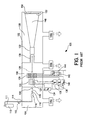
- FIG. 1 shows a schematic of the basic elements of a typical configuration for a GCIB processor 100 of a form known in prior art, and which may be described as follows: a vacuum vessel 102 is divided into three communicating chambers, a source chamber 104, an ionization/acceleration chamber 106, and a processing chamber 108. The three chambers are evacuated to suitable operating pressures by vacuum pumping systems 146a, 146b, and 146c, respectively.
- a condensable source gas 112 (for example argon or N 2 ) stored in a gas storage cylinder 111 is admitted under pressure through gas metering valve 113 and gas feed tube 114 into stagnation chamber 116 and is ejected into the substantially lower pressure vacuum through a properly shaped nozzle 110.
- a supersonic gas jet 118 results. Cooling, which results from the expansion in the jet, causes a portion of the gas jet 118 to condense into clusters, each consisting of from several to several thousand weakly bound atoms or molecules.
- a gas skimmer aperture 120 partially separates the gas molecules that have not condensed into a cluster jet from the cluster jet so as to minimize pressure in the downstream regions where such higher pressures would be detrimental (e.g., ionizer 122, high voltage electrodes 126, and process chamber 108).
- Suitable condensable source gases 112 include, but are not necessarily limited to argon, nitrogen, carbon dioxide, oxygen, and other gases.
- the ionizer 122 is typically an electron impact ionizer that produces thermoelectrons from one or more incandescent filaments 124 and accelerates and directs the electrons causing them to collide with the gas clusters in the gas jet 118, where the jet passes through the ionizer 122.
- the electron impact ejects electrons from the clusters, causing a portion the clusters to become positively ionized.
- a set of suitably biased high voltage electrodes 126 extracts the cluster ions from the ionizer, forming a beam, then accelerates them to a desired energy (typically from 1 keV to several tens of keV) and focuses them to form a GCIB 128.
- Filament power supply 136 provides voltage V F to heat the ionizer filament 124.
- Anode power supply 134 provides voltage V A to accelerate thermoelectrons emitted from filament 124 to cause them to irradiate the cluster containing gas jet 118 to produce ions.
- Extraction power supply 138 provides voltage V E to bias a high voltage electrode to extract ions from the ionizing region of ionizer 122 and to form a GCIB 128.
- Accelerator power supply 140 provides voltage V Acc to bias a high voltage electrode with respect to the ionizer 122 so as to result in a total GCIB acceleration energy equal to V Acc electron volts (eV).
- One or more lens power supplies may be provided to bias high voltage electrodes with potentials (V L1 and V L2 for example) to focus the GCIB 128.
- a workpiece 152 which may be a semiconductor wafer or other workpiece to be processed by GCIB processing, is held on a workpiece holder 150, disposed in the path of the GCIB 128. Since most applications contemplate the processing of large workpieces with spatially uniform results, a scanning system is desirable to uniformly scan the GCIB 128 across large areas to produce spatially homogeneous results. Two pairs of orthogonally oriented electrostatic scan plates 130 and 132 can be utilized to produce a raster or other scanning pattern across the desired processing area. When beam scanning is performed, the GCIB 128 is converted into a scanned GCIB 148, which scans the entire surface of workpiece 152.
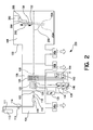
- FIG 2 shows a schematic of the basic elements of an improved configuration for a mechanical scanning GCIB processor 200, which uses a mechanical scanning technique to scan the workpiece relative to the GCIB.
- GCIB formation is essentially as shown in Figure 1, but in mechanical scanning GCIB processor 200 of Figure 2, the GCIB 128 is stationary (not scanned) and the workpiece 152 is mechanically scanned through the GCIB 128 to distribute the effects of the GCIB 128 over a surface of the workpiece 152.
- An X-scan actuator 202 provides linear motion of the workpiece holder 150 in the direction of X-scan motion 208 (into and out of the plane of the paper).
- a Y-scan actuator 204 provides linear motion of the workpiece holder 150 in the direction of Y-scan motion 210, which is orthogonal to the X-scan motion 208.
- the combination of X-scanning and Y-scanning motions moves the workpiece 152, held by the workpiece holder 150 in a raster-like scanning motion through GCIB 128 to cause a uniform irradiation of a surface of the workpiece 152 by the GCIB 128 for uniform processing of the workpiece 152.
- the workpiece holder 150 disposes the workpiece at an angle with respect to the axis of the GCIB 128 so that the GCIB 128 has an angle of beam incidence 206 with respect to the workpiece 152 surface.
- the angle of beam incidence 206 may be 90 degrees or some other angle, preferably 90 degrees or near 90 degrees.
- the workpiece 152 held by workpiece holder 150 moves from the position shown to the alternate position "A", indicated by the designators 152A and 150A respectively. Notice that in moving between the two positions, the workpiece 152 is scanned through the GCIB 128 and in both extreme positions, is moved completely out of the path of the GCIB 128 (over-scanned).
- similar scanning and over-scan is performed in the orthogonal X-scan motion 208 direction (in and out of the plane of the paper) as will be discussed later in discussion of Figure 4B.
- FIG. 3 shows the improved GCIB processing system 300 of the present invention.
- a GCIB generating system 302 is summarized schematically as a block.
- the GCIB generating system 302 can be any of a variety of sources of GCIB having functionality similar to that of the components shown in the source chamber 104 and in the ionizing/acceleration chamber 106 of the mechanical scanning GCIB processor 200 of Figure 2.
- GCIB 128 is generated by GCIB generating system 302.
- the workpiece 152, workpiece holder 150, X-scan actuator 202 and Y-scan actuator 204 are all disposed and function as described for the mechanical scanning GCIB processor 200 of Figure 2.
- a neutralizer 310 disposes one or more thermionic filaments (two shown for example, not for limitation, as first filament 312 and second filament 314, disposed radially about and parallel to the GCIB 128) near the path of the GCIB 128.
- the neutralizer 310 has been shown as a thermionic neutralizer for example, it is recognized that other types of neutralizers may be used as part of the present invention, provided that the neutralizer be controllable to increase or decrease the electron output for neutralization.
- Such alternate neutralizers known in the ion beam art include, but are not limited to, an accel-decel electron guns and various plasma devices such as a plasma electron flood.
- a controllable neutralizer power supply 346 having a control signal input 358 provides controllable filament current 318 symbolized by I F for heating the filaments 312 and 314 through leads 326 and 328.
- Some thermoelectrons 336 emitted by the heated thermionic filaments 312 and 314 are attracted to the positive space charge of the positively charged GCIB 128 and flow along the GCIB 128, reducing the space charge of GCIB 128 and providing a source of electrons to the workpiece 152 to reduce positive charging thereof by the GCIB 128, by neutralizing positive charges that could otherwise accumulate on the workpiece 152.
- a GCIB defining aperture 332 defines GCIB 128 to limit the extent of GCIB 128 downstream of the GCIB defining aperture 332 to assure that the entire extent of GCIB 128 can pass through GCIB sensor aperture 338 into a Faraday cup 306.
- Faraday cup 306 has a suppression electrode 308 and a grounded enclosure 304 and is disposed in the path of GCIB 128 downstream of the GCIB defining aperture 332 and the GCIB sensor aperture 338 so as to collect sensor current 342, symbolized as I S , for measurement.
- a first single-pole double-throw switch 322 having a charging measurement position identified "C” and having a dosimetry measurement position identified “D” controllably connects sensor current 342 to either of resistor 330 via lead 316, or through lead 354 to sensing input 360 of dosimetry and scanner control system 500.
- Resistor 330 may have a value of, for example, 1 Megohm.
- a second single-pole double-throw switch 320 having a charging measurement position identified “C” and having a dosimetry measurement position identified “D” controllably connects suppression electrode 308 to suppression power supply 344 or to ground.
- Switches 320 and 322 are ganged and together controlled by switch controller 324 for simultaneous actuation. Switches 320 and 322 are either both switched to position “C” or both switched to position "D".
- switch 320 and 322 are both switched to position "D".
- sensor current 342 (I S ) is connected to dosimetry and scanner control system 500 and suppression electrode 308 is connected to suppression power supply 344 and thereby biased negative with an electrical potential, suppressor voltage V S , which may be 1500 volts, for example.
- suppressor voltage V S which may be 1500 volts, for example.
- suppression electrode 308 is biased negative, it prevents entry of or exit of electrons to/from the Faraday cup 306 and sensor current 342 (I S ) is a measure of the GCIB current.
- switch 320 and 322 are both switched to position "C".
- sensor current 342 (I S ) is connected through lead 316 to resistor 330 as well as to the non-inverting input of amplifier 348; also suppression electrode 308 is connected to ground and is without bias.
- suppression electrode 308 When suppression electrode 308 is unbiased, it permits entry or exit of electrons to/from the Faraday cup 306 and sensor current 342 (I S ) is a measure of the GCIB current plus electron currents flowing into and out of the Faraday cup 306. This sum of GCIB and electron currents approximates the total current available for charging a workpiece.
- Amplifier 348 has a high input-impedance non-inverting input and amplifies the voltage drop across resistor 330 due to sensor current 342 (I S ) flowing to ground through resistor 330.
- Amplifier 348 has a gain A 1 and outputs charging signal S C proportional to the available workpiece charging current.
- Lead 340 connects charging signal S C to the charging signal input 384 of charge alarm system 350 and to the sample signal input 366 of track-hold module 364.
- Charge alarm system 350 has an alarm output 386 and produces an alarm signal S A at alarm output 386 if the magnitude of S C exceeds a preset value previously experimentally determined to be detrimental to the workpiece 152.
- Lead 352 connects alarm signal S A from alarm output 386 of charge alarm system 350 to alarm signal input 362 of dosimetry and scanner control system 500.
- the charge alarm system 350 may optionally also produce audible and/or visual alarm indications when it produces an alarm signal S A , to notify a human equipment operator that a possible workpiece charging condition exists.
- Track-hold module 364 has a track/hold command input 370 for receiving a track/hold signal S T/H through lead 374 from track hold command output 376 of dosimetry and scanner control system 500 to cause track-hold module 364 to controllably track or hold the signal S C .
- the tracked or held value of signal S C is output as charging track/hold signal S CH , at the track/hold output 368 of track-hold module 364.
- Lead 372 connects charging track/hold signal S CH to control input 358 of neutralizer power supply 346 and to indicator device 356. Responsive to an increase in signal S CH at control input 358, neutralizer power supply 346, produces increasing filament current 318 (I F ) in thermionic filaments 312 and 314, resulting in increased thermionic emission of thermoelectrons 336, with corresponding increasing availability of electrons to neutralize GCIB 128 space charge and to reduce the net current available for workpiece charging. Indicator device 356 displays an indication of the magnitude of charging track/hold signal S CH , which is an indication of current available for charging workpiece 152.
- Dosimetry and scanner control system 500 has scanner control outputs 378 for outputting scanner control signals on cable 334 to control the X-scan actuator 202 and the Y-scan actuator 204. Dosimetry and scanner control system 500 also has a switch control output 380 for outputting a C/D switch control signal, S C/D , through lead 382 to switch controller 324. The functionality of dosimetry and scanner control system 500 is explained hereinafter during the discussion of Figure 5.
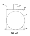
- Figure 4A is a normal view 400 of the workpiece holder 150 of the present invention, with a workpiece 152 in place.
- the workpiece holder 150 may use electrostatic attraction (an electrostatic chuck) to retain the workpiece 152 or may use gravity or a clamp or other arrangement to hold the workpiece in position on the workpiece holder 150.
- a first retaining pin 402 and a second retaining pin 404 may optionally be used to help retain the workpiece 152 on the workpiece holder.
- Figure 4B is a normal view 450 of the workpiece holder 150 of the present invention showing the relationship of a GCIB 128 (as shown in Figures 2 and 3) scan path 452 (indicated by dotted serpentine path) relative to workpiece holder 150 and to a workpiece 152.
- a GCIB 128 as shown in Figures 2 and 3
- scan path 452 indicated by dotted serpentine path
- the angle of beam incidence 206 as defined in Figure 2 is 90 degrees, however the invention is not limited to 90 degrees angle of beam incidence 206.
- the workpiece holder 150 has a bottom edge 468.
- the scan path 452 represents the path that the center of the GCIB takes shown relative to the workpiece holder 150 and workpiece 152 as the workpiece holder is mechanically scanned through the GCIB 128 by X-scan actuator 202 and Y-scan actuator 204 (both as shown in Figures 2 and 3) during GCIB processing of the workpiece.
- a preliminary position 454 represents the position of the center of GCIB 128 prior to commencing processing.
- Start position 456 represents the position of the center of GCIB 128 at the commencement of controlled processing.
- Finish position 466 represents the position of the center of GCIB 128 at the finish or end of processing.
- Preliminary position 454 may be distinct from start position 456, as shown in Figure 4B, or the start position 456 may serve as the preliminary position.
- Dotted circles 458a, 458b, 458c, and 458d represent the envelope of the projection of the GCIB envelope (known as the beam spot) on the plane of the front surface of the workpiece holder 150.
- the GCIB 128 completely over-scans the workpiece 152 on all sides. Along the bottom edge 468 of the workpiece holder 150, the GCIB 128 also completely over-scans the bottom edge 468 of the workpiece holder 150.
- N is shown to be 34 passes for example only, not for limitation. The value of N is not particularly critical and may be chosen to provide adequate overlap of successive scan passes to result in an acceptable degree of uniformity of processing by the GCIB.
- the scan path makes X-axis distance increments 464 i , 464 i+1' 464 i+2 , ...
- V X (N/2)-1.
- the X-direction scan speed, V X in the direction of the X-motion increments is not particularly important and is chosen for design simplicity, since the GCIB 128 is always off of the workpiece 152 during the X-scan motions because of the over-scan.
- the entire beam spot of GCIB 128 is scanned beyond the bottom edge 468 of workpiece holder 150 and the GCIB 128 passes downstream of the workpiece holder 150 and enters the Faraday cup 306 (as shown in Figure 3). At such times, the Faraday cup 306 collects sensor current 342, I S , for measurement.
- sensor current 342, I S may be used for measuring the GCIB 128 beam current, I B , or the total current, I T , (including electrons) available for charging the workpiece, depending on the "D" or "C” position selection of switches 320 and 322 as shown in Figure 3 and described above.
- the scan path 452 has been shown as a serpentine path, with beam travel in X-scan and Y-scan directions and describing an overall rectangularly shaped scanned area A S . It is recognized that the invention is not limited to the above-described scan path 452.
- Other two-axis scan paths describing scan patterns of area A S generated by constant or varying velocities in the two axes and producing rectangular or non-rectangular scanned area, even including spiral patterns may be utilized provided that the pattern includes at least one complete overscan such that the entire beam spot of GCIB 128 is scanned beyond an edge of the workpiece holder 150 and enters the Faraday cup 306 for measurement.
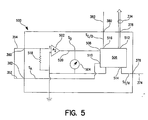
- Figure 5 represents a schematic of details of the dosimetry and scanning control system 500 of Figure 3.
- dosimetry and scanner control system 500 has a sensing input 360 for receiving sensor current 342, I S , on lead 354.
- I S is a measure of the GCIB 128 current, I B .
- Sensor current 342 (I S ) is connected through lead 354 to resistor 518 as well as to non-inverting input of amplifier 502.
- Resistor 518 may have a value of 1 Megohm, for example, not for limitation.
- Amplifier 502 has a gain A 2 and outputs dosimetry signal S D proportional to the beam current, I B , of GCIB 128.
- Lead 520 connects dosimetry signal S D to the dosimetry input 508 of dosimetry/scan controller 506 and also to indicator device 504.
- Indicator device 504 indicates the magnitude of the beam current, I B , of GCIB 128.
- Dosimetry/scan controller 506 has an alarm input 510 for receiving alarm signal, S A , on lead 352 through alarm signal input 362 of dosimetry and scanner control system 500.
- Dosimetry/scan controller 506 has a track/hold signal output 514 for outputting a track/hold signal, S T/H, on lead 374 through track/hold command output 376 of dosimetry and scanner control system 500.
- Dosimetry/scan controller 506 has a C/D switch control output 516 for outputting a C/D switch control signal, S C/D , on lead 382 through switch control output 380 of dosimetry and scanner control system 500.
- Dosimetry/scan controller 506 has a scanner control output bus 512 for outputting scanner control signals on cable 334 through scanner control outputs 378 of dosimetry and scanner control system 500.
- dosimetry/scan controller 506 may optionally be a shared part of the functionality and apparatus of a microprocessor system or microcomputer or general purpose controller that also controls other functions of the GCIB processing system 300.
- a GCIB 128 is established in GCIB processing system 300, with workpiece holder 150 positioned in preliminary position 454. Accordingly, GCIB 128 passes into Faraday cup 306.
- Dosimetry/scan controller 506 outputs a signal, S C/D to cause switch controller 324 to set switches 320 and 322 to the charging measurement position "C". Then dosimetry/scan controller 506 outputs a track/hold signal, S T/H , to cause the track/hold output 368 of track-hold module 364 to track charging signal S C . Accordingly, indicator device 356 and neutralizer power supply 346 receive S CH , which tracks S C .
- thermoelectrons 336 A negative feedback loop is closed through the emission of thermoelectrons 336. Sensor current 342, I S , is minimized by the feedback. If the system is functioning properly, charging signal S C is minimized and charge alarm system 350 does not output an alarm or alarm signal S A . After a time delay adequate to permit settling of the S C signal (typically a second to a few seconds), dosimetry/scan controller 506 tests alarm signal S A at alarm input 510 to assure that the total current available to charge the workpiece 152 is at a safe level.
- dosimetry/scan controller 506 When dosimetry/scan controller 506 has determined that there is no alarm signal S A , it outputs a track/hold signal, S T/H , to cause the track/hold output 368 of track-hold module 364 to hold the charging track/hold signal, S CH' fixed for the duration of the GCIB processing of the workpiece 152.
- Dosimetry/scan controller 506 next outputs a signal, S C/D to cause switch controller 324 to set switches 320 and 322 to the dosimetry position "D". Accordingly, dosimetry input 508 of dosimetry/scan controller 506 receives dosimetry signal S D . Dosimetry/scan controller measures the value of dosimetry signal S D (in amps of beam current, I B , typically a few microamps to a few thousand microamps). Dosimetry/scan controller 506 has a previously stored, predetermined, required processing dose, D P , (measured in amp-seconds per unit area) for GCIB processing of the workpiece 152 to achieve the desired processing effect.
- D P predetermined, required processing dose
- Dosimetry/scan controller 506 then sends signals through scanner control output bus 512 through scanner control outputs 378 through cable 334 to cause X-scan actuator 202 and Y-scan actuator 204 to produce controlled X-scan motions and Y-scan motions with controlled speeds, first from preliminary position 454 to start position 456, then along scan path 452 to finish position 466. Each Y-scan motion is performed at a controlled Y-scan speed V Y .
- the scan path 452 (see Figure 4B) is generated.
- the finish position 466 has been achieved, the processing of the workpiece 152 is complete and processing dose D P has been applied uniformly to the entire workpiece 152, and with minimized charging of the workpiece 152.
Description
- This invention relates generally to dosimetry and workpiece neutralization for ion beam processing of workpieces, and, more particularly to dosimetry and workpiece neutralization for gas cluster ion beam (GCIB) processing.
- The use of a GCIB for etching, cleaning, and smoothing of the surfaces of various materials is known in the art (See for example, US patent 5,814,194, Deguchi, et al., "Substrate Surface Treatment Method", 1998). Means for creation of and acceleration of such GCIBs are also described in the Deguchi reference. It is also known (US patent 5,459,326, Yamada, "Method for Surface Treatment with Extra-Low-Speed Ion Beam", 1995) that atoms in a cluster ion are not individually energetic enough (on the order of a few electron volts) to significantly penetrate a surface to cause the residual sub-surface damage typically associated with the other types of ion beam processing in which individual ions may have energies on the order of thousands of electron volts. Nevertheless, the cluster ions themselves can be made sufficiently energetic (some thousands of electron volts), to effectively etch, smooth or clean surfaces as shown by Yamada & Matsuo (in "Cluster ion beam processing", Matl. Science in Semiconductor Processing I, (1998) pp 27-41).
- Since GCIBs contain ionized particles that carry electrical charge, a measure of the processing dose a workpiece receives is the amount of charge (amp-seconds) received by a unit area of the workpiece, measured in amp-seconds per square centimeter, for example. For insulating, partly insulating, or semiconductive workpieces, ion beam processing can induce charging of the workpiece undergoing ion beam processing. An advantage of GCIB processing over some more conventional ion beam processes is that, because of the relatively large mass to charge ratio of the cluster ions compared to conventional atomic or molecular ions, processing can often be effected with less transfer of charge to the workpiece. Nevertheless, workpiece charging is still a concern and means are needed to reduce the degree of such charging during GCIB processing of workpieces.
- It is therefore an object of this invention to provide apparatus and methods for measuring and controlling the processing dose received by a workpiece.
- It is a further object of this invention to measure and control the amount of charge or surface charging that is or may be received by a workpiece during GCIB processing.
- The objects set forth above as well as further and other objects and advantages of the present invention are achieved by the embodiments of the invention described hereinbelow.
- A gas cluster ion beam processing apparatus treats a workpiece with a gas cluster ion beam to effect surface modification such as smoothing, etching, cleaning, deposition, etc. A neutralizer is provided to reduce surface charging of the workpiece by the GCIB. A single Faraday cup sensor is used to measure the GCIB current for dosimetry and scanning uniformity control and also to measure and control the degree of surface charging that may be induced in the workpiece during processing.
- To insure uniform processing, X-Y mechanical scanning of the workpiece relative to the GCIB is used to distribute the beam effects over the surface or the workpiece. The mechanical scanning mechanism moves the workpiece in an orthogonal raster pattern through the GCIB and also out of the beam at least once each processing cycle. At that time, the GCIB current is measured by an electron suppressed Faraday cup. However, with an improved switching and control technique, the Faraday cup can also be used to measure the total current for workpiece charging and, thus, may control a charge neutralization system or provide a display and an alarm and/or interlock to indicate an undesirable workpiece charging condition. To provide this charging current sensing feature, the suppression voltage on the Faraday cup bias ring is removed. This allows electrons as well as gas cluster ions to be sensed by the Faraday cup. Measurement of the charging can then be accomplished by measuring the net current in the Faraday cup.
- For a better understanding of the present invention, together with other and further objects thereof, reference is made to the accompanying drawings and detailed description and its scope will be pointed out in the appended claims.
-
- Figure 1 is a schematic showing the basic elements of a prior art GCIB processing apparatus that uses an electrostatically scanned beam;
- Figure 2 is a schematic showing the basic elements of a GCIB processing apparatus of the present invention that uses mechanical scanning of a workpiece to distribute the effect of a GCIB over a surface of a workpiece;
- Figure 3 is a schematic of a GCIB processing system having charging control and dose measurement and control improvements of the present invention;
- Figure 4A is a normal view of the workpiece holder of the present invention, with a workpiece in place;
- Figure 4B is a normal view of the workpiece holder of the present invention showing the relationship of a GCIB scanning pattern relative to workpiece holder and workpiece; and
- Figure 5 represents a schematic of details of the dosimetry and scanning control portions of the present invention.
- Figure 1 shows a schematic of the basic elements of a typical configuration for a
GCIB processor 100 of a form known in prior art, and which may be described as follows: avacuum vessel 102 is divided into three communicating chambers, asource chamber 104, an ionization/acceleration chamber 106, and aprocessing chamber 108. The three chambers are evacuated to suitable operating pressures byvacuum pumping systems gas storage cylinder 111 is admitted under pressure throughgas metering valve 113 andgas feed tube 114 intostagnation chamber 116 and is ejected into the substantially lower pressure vacuum through a properly shapednozzle 110. Asupersonic gas jet 118 results. Cooling, which results from the expansion in the jet, causes a portion of thegas jet 118 to condense into clusters, each consisting of from several to several thousand weakly bound atoms or molecules. Agas skimmer aperture 120 partially separates the gas molecules that have not condensed into a cluster jet from the cluster jet so as to minimize pressure in the downstream regions where such higher pressures would be detrimental (e.g.,ionizer 122,high voltage electrodes 126, and process chamber 108). Suitablecondensable source gases 112 include, but are not necessarily limited to argon, nitrogen, carbon dioxide, oxygen, and other gases. - After the
supersonic gas jet 118 containing gas clusters has been formed, the clusters are ionized in anionizer 122. Theionizer 122 is typically an electron impact ionizer that produces thermoelectrons from one or moreincandescent filaments 124 and accelerates and directs the electrons causing them to collide with the gas clusters in thegas jet 118, where the jet passes through theionizer 122. The electron impact ejects electrons from the clusters, causing a portion the clusters to become positively ionized. A set of suitably biasedhigh voltage electrodes 126 extracts the cluster ions from the ionizer, forming a beam, then accelerates them to a desired energy (typically from 1 keV to several tens of keV) and focuses them to form aGCIB 128.Filament power supply 136 provides voltage VF to heat theionizer filament 124.Anode power supply 134 provides voltage VA to accelerate thermoelectrons emitted fromfilament 124 to cause them to irradiate the cluster containinggas jet 118 to produce ions.Extraction power supply 138 provides voltage VE to bias a high voltage electrode to extract ions from the ionizing region ofionizer 122 and to form aGCIB 128.Accelerator power supply 140 provides voltage VAcc to bias a high voltage electrode with respect to theionizer 122 so as to result in a total GCIB acceleration energy equal to VAcc electron volts (eV). One or more lens power supplies (142 and 144 shown for example) may be provided to bias high voltage electrodes with potentials (VL1 and VL2 for example) to focus theGCIB 128. - A
workpiece 152, which may be a semiconductor wafer or other workpiece to be processed by GCIB processing, is held on aworkpiece holder 150, disposed in the path of the GCIB 128. Since most applications contemplate the processing of large workpieces with spatially uniform results, a scanning system is desirable to uniformly scan theGCIB 128 across large areas to produce spatially homogeneous results. Two pairs of orthogonally orientedelectrostatic scan plates GCIB 148, which scans the entire surface ofworkpiece 152. - Figure 2 shows a schematic of the basic elements of an improved configuration for a mechanical scanning GCIB
processor 200, which uses a mechanical scanning technique to scan the workpiece relative to the GCIB. GCIB formation is essentially as shown in Figure 1, but in mechanical scanning GCIBprocessor 200 of Figure 2, the GCIB 128 is stationary (not scanned) and theworkpiece 152 is mechanically scanned through theGCIB 128 to distribute the effects of theGCIB 128 over a surface of theworkpiece 152. AnX-scan actuator 202 provides linear motion of theworkpiece holder 150 in the direction of X-scan motion 208 (into and out of the plane of the paper). A Y-scan actuator 204 provides linear motion of theworkpiece holder 150 in the direction of Y-scan motion 210, which is orthogonal to theX-scan motion 208. The combination of X-scanning and Y-scanning motions moves theworkpiece 152, held by theworkpiece holder 150 in a raster-like scanning motion through GCIB 128 to cause a uniform irradiation of a surface of theworkpiece 152 by the GCIB 128 for uniform processing of theworkpiece 152. Theworkpiece holder 150 disposes the workpiece at an angle with respect to the axis of theGCIB 128 so that the GCIB 128 has an angle ofbeam incidence 206 with respect to theworkpiece 152 surface. The angle ofbeam incidence 206 may be 90 degrees or some other angle, preferably 90 degrees or near 90 degrees. During Y-scanning, theworkpiece 152 held byworkpiece holder 150 moves from the position shown to the alternate position "A", indicated by thedesignators 152A and 150A respectively. Notice that in moving between the two positions, theworkpiece 152 is scanned through the GCIB 128 and in both extreme positions, is moved completely out of the path of the GCIB 128 (over-scanned). Though not shown explicitly in Figure 2, similar scanning and over-scan is performed in theorthogonal X-scan motion 208 direction (in and out of the plane of the paper) as will be discussed later in discussion of Figure 4B. - Figure 3 shows the improved
GCIB processing system 300 of the present invention. AGCIB generating system 302 is summarized schematically as a block. TheGCIB generating system 302 can be any of a variety of sources of GCIB having functionality similar to that of the components shown in thesource chamber 104 and in the ionizing/acceleration chamber 106 of the mechanicalscanning GCIB processor 200 of Figure 2. Referring again to Figure 3,GCIB 128 is generated byGCIB generating system 302. Theworkpiece 152,workpiece holder 150,X-scan actuator 202 and Y-scan actuator 204 are all disposed and function as described for the mechanicalscanning GCIB processor 200 of Figure 2. Aneutralizer 310 disposes one or more thermionic filaments (two shown for example, not for limitation, asfirst filament 312 andsecond filament 314, disposed radially about and parallel to the GCIB 128) near the path of theGCIB 128. Although theneutralizer 310 has been shown as a thermionic neutralizer for example, it is recognized that other types of neutralizers may be used as part of the present invention, provided that the neutralizer be controllable to increase or decrease the electron output for neutralization. Such alternate neutralizers known in the ion beam art include, but are not limited to, an accel-decel electron guns and various plasma devices such as a plasma electron flood. In the present example of athermionic neutralizer 310, a controllableneutralizer power supply 346 having acontrol signal input 358 provides controllable filament current 318 symbolized by IF for heating thefilaments leads thermoelectrons 336 emitted by the heatedthermionic filaments GCIB 128 and flow along theGCIB 128, reducing the space charge ofGCIB 128 and providing a source of electrons to theworkpiece 152 to reduce positive charging thereof by theGCIB 128, by neutralizing positive charges that could otherwise accumulate on theworkpiece 152. AGCIB defining aperture 332 definesGCIB 128 to limit the extent ofGCIB 128 downstream of theGCIB defining aperture 332 to assure that the entire extent ofGCIB 128 can pass throughGCIB sensor aperture 338 into aFaraday cup 306.Faraday cup 306 has asuppression electrode 308 and a groundedenclosure 304 and is disposed in the path ofGCIB 128 downstream of theGCIB defining aperture 332 and theGCIB sensor aperture 338 so as to collect sensor current 342, symbolized as IS, for measurement. - A first single-pole double-throw switch 322 having a charging measurement position identified "C" and having a dosimetry measurement position identified "D" controllably connects sensor current 342 to either of
resistor 330 vialead 316, or throughlead 354 to sensinginput 360 of dosimetry andscanner control system 500.Resistor 330 may have a value of, for example, 1 Megohm. - A second single-pole double-
throw switch 320 having a charging measurement position identified "C" and having a dosimetry measurement position identified "D" controllably connectssuppression electrode 308 tosuppression power supply 344 or to ground. -
Switches 320 and 322 are ganged and together controlled byswitch controller 324 for simultaneous actuation.Switches 320 and 322 are either both switched to position "C" or both switched to position "D". - When dosimetry measurement is required, switches 320 and 322 are both switched to position "D". Hence sensor current 342 (IS) is connected to dosimetry and
scanner control system 500 andsuppression electrode 308 is connected tosuppression power supply 344 and thereby biased negative with an electrical potential, suppressor voltage VS, which may be 1500 volts, for example. Whensuppression electrode 308 is biased negative, it prevents entry of or exit of electrons to/from theFaraday cup 306 and sensor current 342 (IS) is a measure of the GCIB current. - When measurement of approximate workpiece charging current is required, switches 320 and 322 are both switched to position "C". Hence sensor current 342 (IS) is connected through
lead 316 toresistor 330 as well as to the non-inverting input ofamplifier 348; alsosuppression electrode 308 is connected to ground and is without bias. Whensuppression electrode 308 is unbiased, it permits entry or exit of electrons to/from theFaraday cup 306 and sensor current 342 (IS) is a measure of the GCIB current plus electron currents flowing into and out of theFaraday cup 306. This sum of GCIB and electron currents approximates the total current available for charging a workpiece.Amplifier 348 has a high input-impedance non-inverting input and amplifies the voltage drop acrossresistor 330 due to sensor current 342 (IS) flowing to ground throughresistor 330.Amplifier 348 has a gain A1 and outputs charging signal SC proportional to the available workpiece charging current.Lead 340 connects charging signal SC to the chargingsignal input 384 ofcharge alarm system 350 and to thesample signal input 366 of track-hold module 364.Charge alarm system 350 has analarm output 386 and produces an alarm signal SA atalarm output 386 if the magnitude of SC exceeds a preset value previously experimentally determined to be detrimental to theworkpiece 152.Lead 352 connects alarm signal SA fromalarm output 386 ofcharge alarm system 350 to alarmsignal input 362 of dosimetry andscanner control system 500. Thecharge alarm system 350 may optionally also produce audible and/or visual alarm indications when it produces an alarm signal SA, to notify a human equipment operator that a possible workpiece charging condition exists. Track-hold module 364 has a track/hold command input 370 for receiving a track/hold signal ST/H throughlead 374 from trackhold command output 376 of dosimetry andscanner control system 500 to cause track-hold module 364 to controllably track or hold the signal SC. The tracked or held value of signal SC is output as charging track/hold signal SCH, at the track/hold output 368 of track-hold module 364.Lead 372 connects charging track/hold signal SCH to controlinput 358 ofneutralizer power supply 346 and to indicator device 356. Responsive to an increase in signal SCH atcontrol input 358,neutralizer power supply 346, produces increasing filament current 318 (IF) inthermionic filaments thermoelectrons 336, with corresponding increasing availability of electrons to neutralizeGCIB 128 space charge and to reduce the net current available for workpiece charging. Indicator device 356 displays an indication of the magnitude of charging track/hold signal SCH, which is an indication of current available for chargingworkpiece 152. Dosimetry andscanner control system 500 hasscanner control outputs 378 for outputting scanner control signals oncable 334 to control theX-scan actuator 202 and the Y-scan actuator 204. Dosimetry andscanner control system 500 also has aswitch control output 380 for outputting a C/D switch control signal, SC/D, throughlead 382 to switchcontroller 324. The functionality of dosimetry andscanner control system 500 is explained hereinafter during the discussion of Figure 5. - Figure 4A is a
normal view 400 of theworkpiece holder 150 of the present invention, with aworkpiece 152 in place. Theworkpiece holder 150 may use electrostatic attraction (an electrostatic chuck) to retain theworkpiece 152 or may use gravity or a clamp or other arrangement to hold the workpiece in position on theworkpiece holder 150. Afirst retaining pin 402 and asecond retaining pin 404 may optionally be used to help retain theworkpiece 152 on the workpiece holder. - Figure 4B is a
normal view 450 of theworkpiece holder 150 of the present invention showing the relationship of a GCIB 128 (as shown in Figures 2 and 3) scan path 452 (indicated by dotted serpentine path) relative toworkpiece holder 150 and to aworkpiece 152. For purposes of this figure and this discussion it has been assumed that the angle ofbeam incidence 206 as defined in Figure 2 is 90 degrees, however the invention is not limited to 90 degrees angle ofbeam incidence 206. Theworkpiece holder 150 has abottom edge 468. The scan path 452 represents the path that the center of the GCIB takes shown relative to theworkpiece holder 150 andworkpiece 152 as the workpiece holder is mechanically scanned through theGCIB 128 byX-scan actuator 202 and Y-scan actuator 204 (both as shown in Figures 2 and 3) during GCIB processing of the workpiece. Apreliminary position 454 represents the position of the center ofGCIB 128 prior to commencing processing. Startposition 456 represents the position of the center ofGCIB 128 at the commencement of controlled processing. Finishposition 466 represents the position of the center ofGCIB 128 at the finish or end of processing.Preliminary position 454 may be distinct fromstart position 456, as shown in Figure 4B, or thestart position 456 may serve as the preliminary position.Dotted circles workpiece holder 150. TheGCIB 128 completely over-scans theworkpiece 152 on all sides. Along thebottom edge 468 of theworkpiece holder 150, theGCIB 128 also completely over-scans thebottom edge 468 of theworkpiece holder 150. Between thestart position 456 and thefinish position 466, the scan path 452 covers a scanned area, AS = DX x DY, where DX and DY are indicated by thedesignators start position 456 and thefinish position 466, the scan path 452 of the center of theGCIB 128 makes a predetermined number, N, passes across theworkpiece holder 150 in the Y-axis direction. Each of the N passes is of length 462 (DY). In Figure 4B, N is shown to be 34 passes for example only, not for limitation. The value of N is not particularly critical and may be chosen to provide adequate overlap of successive scan passes to result in an acceptable degree of uniformity of processing by the GCIB. In general, smaller beam diameters and larger workpieces require larger values of N to provide good processing uniformity. At the Y-position extremes of each of the N passes of the scan path 452, the path moves (relative to the workpiece holder 150) in the X-axis direction by an X-axis distance increment 470 IX, where IX = DX /(N-1), where DX is thelength 460. - The Y-direction scan speed, VY, is controlled to be substantially constant during each of the N passes in the Y-axis direction. Accordingly, the time per scan pass in the Y-axis direction has a constant value TY and the total time of the N Y-direction scans is TS = N x TY, and the Y-scan motion speed is given by VY = (N x DY) /TS. At the Y-position extremes near the
bottom edge 468 of theworkpiece holder 150, of each of the N passes of the scan path 452, the scan path makesX-axis distance increments GCIB 128 is always off of theworkpiece 152 during the X-scan motions because of the over-scan. At all of the times when the center of theGCIB 128 is atpreliminary position 454, or atstart position 456, or atfinish position 466, or at any of theX-axis distance increments 464 near thebottom edge 468 ofworkpiece holder 150, the entire beam spot ofGCIB 128 is scanned beyond thebottom edge 468 ofworkpiece holder 150 and theGCIB 128 passes downstream of theworkpiece holder 150 and enters the Faraday cup 306 (as shown in Figure 3). At such times, theFaraday cup 306 collects sensor current 342, IS, for measurement. At any of those such times, sensor current 342, IS, may be used for measuring theGCIB 128 beam current, IB, or the total current, IT, (including electrons) available for charging the workpiece, depending on the "D" or "C" position selection ofswitches 320 and 322 as shown in Figure 3 and described above. Although complete overscan of theworkpiece 152 on all sides is the preferred embodiment for achieving uniform processing of theentire workpiece 152, it is recognized that to it is only necessary to overscan theworkpiece 152 andworkpiece holder 150 in at least one location to practice the present invention. For purposes of explanation, the scan path 452 has been shown as a serpentine path, with beam travel in X-scan and Y-scan directions and describing an overall rectangularly shaped scanned area AS. It is recognized that the invention is not limited to the above-described scan path 452. Other two-axis scan paths describing scan patterns of area AS generated by constant or varying velocities in the two axes and producing rectangular or non-rectangular scanned area, even including spiral patterns may be utilized provided that the pattern includes at least one complete overscan such that the entire beam spot ofGCIB 128 is scanned beyond an edge of theworkpiece holder 150 and enters theFaraday cup 306 for measurement. - Figure 5 represents a schematic of details of the dosimetry and
scanning control system 500 of Figure 3. Referring to Figure 5, dosimetry andscanner control system 500 has asensing input 360 for receiving sensor current 342, IS, onlead 354. During dosimetry measurements, when switches 320 and 322 are set to their respective "D" positions, IS is a measure of theGCIB 128 current, IB. Sensor current 342 (IS) is connected throughlead 354 toresistor 518 as well as to non-inverting input ofamplifier 502.Resistor 518 may have a value of 1 Megohm, for example, not for limitation.Amplifier 502 has a high input-impedance non-inverting input and amplifies the voltage drop acrossresistor 518 due to sensor current 342 (IS = IB) flowing to ground throughresistor 518.Amplifier 502 has a gain A2 and outputs dosimetry signal SD proportional to the beam current, IB, ofGCIB 128.Lead 520 connects dosimetry signal SD to thedosimetry input 508 of dosimetry/scan controller 506 and also toindicator device 504.Indicator device 504 indicates the magnitude of the beam current, IB, ofGCIB 128. - Dosimetry/
scan controller 506 has analarm input 510 for receiving alarm signal, SA, onlead 352 throughalarm signal input 362 of dosimetry andscanner control system 500. - Dosimetry/
scan controller 506 has a track/hold signal output 514 for outputting a track/hold signal, ST/H, onlead 374 through track/hold command output 376 of dosimetry andscanner control system 500. - Dosimetry/
scan controller 506 has a C/Dswitch control output 516 for outputting a C/D switch control signal, SC/D, onlead 382 throughswitch control output 380 of dosimetry andscanner control system 500. - Dosimetry/
scan controller 506 has a scannercontrol output bus 512 for outputting scanner control signals oncable 334 throughscanner control outputs 378 of dosimetry andscanner control system 500. - It is recognized that dosimetry/
scan controller 506 may optionally be a shared part of the functionality and apparatus of a microprocessor system or microcomputer or general purpose controller that also controls other functions of theGCIB processing system 300. - In operation, prior to initiation of GCIB processing of a
workpiece 152, aGCIB 128 is established inGCIB processing system 300, withworkpiece holder 150 positioned inpreliminary position 454. Accordingly,GCIB 128 passes intoFaraday cup 306. Dosimetry/scan controller 506 outputs a signal, SC/D to causeswitch controller 324 to setswitches 320 and 322 to the charging measurement position "C". Then dosimetry/scan controller 506 outputs a track/hold signal, ST/H, to cause the track/hold output 368 of track-hold module 364 to track charging signal SC. Accordingly, indicator device 356 andneutralizer power supply 346 receive SCH, which tracks SC. A negative feedback loop is closed through the emission ofthermoelectrons 336. Sensor current 342, IS, is minimized by the feedback. If the system is functioning properly, charging signal SC is minimized andcharge alarm system 350 does not output an alarm or alarm signal SA. After a time delay adequate to permit settling of the SC signal (typically a second to a few seconds), dosimetry/scan controller 506 tests alarm signal SA atalarm input 510 to assure that the total current available to charge theworkpiece 152 is at a safe level. When dosimetry/scan controller 506 has determined that there is no alarm signal SA, it outputs a track/hold signal, ST/H, to cause the track/hold output 368 of track-hold module 364 to hold the charging track/hold signal, SCH' fixed for the duration of the GCIB processing of theworkpiece 152. - Dosimetry/
scan controller 506 next outputs a signal, SC/D to causeswitch controller 324 to setswitches 320 and 322 to the dosimetry position "D". Accordingly,dosimetry input 508 of dosimetry/scan controller 506 receives dosimetry signal SD. Dosimetry/scan controller measures the value of dosimetry signal SD (in amps of beam current, IB, typically a few microamps to a few thousand microamps). Dosimetry/scan controller 506 has a previously stored, predetermined, required processing dose, DP, (measured in amp-seconds per unit area) for GCIB processing of theworkpiece 152 to achieve the desired processing effect. Other process parameters including the number of scan passes, N, X- and Y-scan distances DX and DY are also predetermined and previously stored in dosimetry/scan controller 506. Dosimetry/scan controller 506 calculates total scan time TS. and scan speed VY according to:


- Dosimetry/
scan controller 506 then sends signals through scannercontrol output bus 512 throughscanner control outputs 378 throughcable 334 to causeX-scan actuator 202 and Y-scan actuator 204 to produce controlled X-scan motions and Y-scan motions with controlled speeds, first frompreliminary position 454 to startposition 456, then along scan path 452 to finishposition 466. Each Y-scan motion is performed at a controlled Y-scan speed VY. The scan path 452 (see Figure 4B) is generated. When thefinish position 466 has been achieved, the processing of theworkpiece 152 is complete and processing dose DP has been applied uniformly to theentire workpiece 152, and with minimized charging of theworkpiece 152. - Although the invention has been described with respect to various embodiments, it should be realized that this invention is also capable of a wide variety of further and other embodiments within the scope of the appended claims.
Claims (9)
- An apparatus (200) utilizing a gas cluster ion beam (128) for processing a surface of a workpiece (152), the apparatus comprising:a vacuum vessel (102);a gas cluster ion beam source (118) within the vacuum vessel (102) for producing a gas cluster ion beam (128) having a beam current;an accelerator (126) for accelerating the gas cluster ion beam (128) along a trajectory;workpiece holding means (150) for holding the work-piece (152) for gas cluster ion beam processing;characterised in that the apparatus (200) further comprises:controllable moving means (202, 204) for selectively scanning said workpiece holding means (150) and the workpiece (152) through said gas cluster ion beam (128) at a location along said trajectory, between said accelerator (126) and a current measurement means disposed along said trajectory, and for selectively removing the workpiece holding means (150) and the workpiece (152) from said gas cluster ion beam trajectory;control means (500) for providing signals to said controllable moving means (202, 204) for scanning the workpiece (152) and for removing the workpiece (152) and the workpiece holding means (150) from said gas cluster ion beam trajectory to allow measurement of said beam current, said control means (500) providing such signals at least in part in, response to at least one current measurement signal (342) acquired by the current measurement means (338); andsaid current measuring means (338) having at least two controllable modes for acquiring sensor current measurement signal (342), one (D) of said modes selectively measuring a sample of the gas cluster ion beam current and another (C) of said modes selectively measuring a sample of the total current available for charging the workpiece (152), said control means (500) providing control signals for selecting between the two modes (C, D).
- An apparatus as claimed in claim 1, wherein said at least one current measurement signal (342) represents a sample of said gas cluster ion beam current measured while the workpiece (152) and said workpiece holder (150) are removed from said gas cluster ion beam trajectory.
- An apparatus as claimed in claim 2, wherein said control means (500) further comprises, responsive to at least one current measurement signal (242) representing a sample of said gas cluster ion beam current(a) output signals (512) for controlling the scanning of the workpiece (152); or(b) output signals (376) to control a dosage of said gas cluster ion beam (128) applied to the workpiece (152) during processing.
- An apparatus as claimed in any of claims 1-3, further comprising a controllable neutralizer (310) for providing electrons (336) to reduce(a) space charge in said gas cluster ion beam (128); or(b) electrical charging of the workpiece (152).
- An apparatus as claimed in claim 1 further comprises a controllable neutralizer (310) for reducing, responsive to control signals output from the control means (500) associated with at least one current measurement signal representing to total current available, the total current available for electrical charging of the workpiece (152) to a predetermined safe level for processing.
- An apparatus as claimed in claim 1, wherein said control means (500) further comprises means for determining whether at least one current measurement signal representing said total current available exceeds a predetermined safe level for processing, and means for preventing processing of the workpiece (152) if said total current exceeds the predetermined safe level for said processing.
- A method of processing the surface of a workpiece (152) using a gas cluster ion beam comprising the steps of:forming a gas cluster ion beam within a vacuum vessel (102), said gas cluster ion beam having a gas cluster ion beam current;accelerating said gas cluster ion beam along a trajectory;controllably holding the workpiece (152) for gas cluster ion beam processing out of the trajectory of said gas cluster ion beam;providing a current measurement means (338) having at least two (C, D) controllable modes, one (D) of said modes for selectively measuring a sample of the gas cluster ion beam current and another (C) of said modes for selectively measuring a sample of the total current available for charging the workpiece (152);selecting said mode for measuring a current sample related to the workpiece (152) processing;measuring, at least once, the current sample;moving, at least once, the workpiece (152) into the trajectory of said gas cluster ion beam (128) for processing; andcontrolling workpiece (152) processing using said at least one measurement of the current sample.
- A method as claimed in claim 7, wherein:said current sample is a sample of the gas cluster ion beam current; the controlling step comprises controlling a dosage of said gas cluster ion beam applied to the workpiece (152).
- A method as claimed in claim 7, wherein:said current sample is a sample of the total current available for workpiece (152) charging; andthe controlling step comprises using said sample of said total current available as a basis for reducing said total current available for the workpiece (152) charging to a predetermined safe level.
Applications Claiming Priority (3)
| Application Number | Priority Date | Filing Date | Title |
|---|---|---|---|
| US25828000P | 2000-12-26 | 2000-12-26 | |
| US258280P | 2000-12-26 | ||
| PCT/US2001/050343 WO2002052608A2 (en) | 2000-12-26 | 2001-12-26 | Charging control and dosimetry system for gas cluster ion beam |
Publications (2)
| Publication Number | Publication Date |
|---|---|
| EP1348227A2 EP1348227A2 (en) | 2003-10-01 |
| EP1348227B1 true EP1348227B1 (en) | 2006-08-16 |
Family
ID=22979888
Family Applications (1)
| Application Number | Title | Priority Date | Filing Date |
|---|---|---|---|
| EP01988402A Expired - Lifetime EP1348227B1 (en) | 2000-12-26 | 2001-12-26 | Charging control and dosimetry system and method for gas cluster ion beam |
Country Status (5)
| Country | Link |
|---|---|
| US (1) | US6646277B2 (en) |
| EP (1) | EP1348227B1 (en) |
| JP (1) | JP4168381B2 (en) |
| DE (1) | DE60122379T2 (en) |
| WO (1) | WO2002052608A2 (en) |
Families Citing this family (72)
| Publication number | Priority date | Publication date | Assignee | Title |
|---|---|---|---|---|
| WO2004027813A1 (en) * | 2002-09-23 | 2004-04-01 | Epion Corporation | System for and method of gas cluster ion beam processing |
| US7410890B2 (en) * | 2002-12-12 | 2008-08-12 | Tel Epion Inc. | Formation of doped regions and/or ultra-shallow junctions in semiconductor materials by gas-cluster ion irradiation |
| WO2004053945A2 (en) * | 2002-12-12 | 2004-06-24 | Epion Corporation | Re-crystallization of semiconductor surface film and doping of semiconductor by energetic cluster irradiation |
| WO2005089459A2 (en) | 2004-03-17 | 2005-09-29 | Epion Corporation | Method and apparatus for improved beam stability in high current gas-cluster ion beam processing system |
| US7060989B2 (en) * | 2004-03-19 | 2006-06-13 | Epion Corporation | Method and apparatus for improved processing with a gas-cluster ion beam |
| US6953942B1 (en) * | 2004-09-20 | 2005-10-11 | Axcelis Technologies, Inc. | Ion beam utilization during scanned ion implantation |
| US7173252B2 (en) * | 2004-10-25 | 2007-02-06 | Epion Corporation | Ionizer and method for gas-cluster ion-beam formation |
| US20060093753A1 (en) * | 2004-10-29 | 2006-05-04 | Nickel Janice H | Method of engineering a property of an interface |
| US7799683B2 (en) * | 2004-11-08 | 2010-09-21 | Tel Epion, Inc. | Copper interconnect wiring and method and apparatus for forming thereof |
| US7504135B2 (en) * | 2005-02-03 | 2009-03-17 | Samsung Electronics Co., Ltd | Method of fabricating a manganese diffusion barrier |
| US7186992B2 (en) * | 2005-02-07 | 2007-03-06 | Hewlett-Packard Development Company, L.P. | Method of fabricating a polarizing layer on an interface |
| EP1890319B1 (en) * | 2005-05-20 | 2011-03-23 | Japan Aviation Electronics Industry, Limited | METHOD FOR FLATTENING a SOLID SURFACE |
| JP5105729B2 (en) * | 2005-09-01 | 2012-12-26 | キヤノン株式会社 | Processing method with gas cluster ion beam |
| KR20080078703A (en) | 2005-12-01 | 2008-08-27 | 텔 에피온 인크 | Method and apparatus for scanning a workpiece through an ion beam |
| US7342240B2 (en) * | 2006-02-24 | 2008-03-11 | Varian Semiconductor Equipment Associates, Inc. | Ion beam current monitoring |
| JP2007277708A (en) * | 2006-03-17 | 2007-10-25 | Canon Inc | Film deposition apparatus and method of film deposition |
| US7420189B2 (en) * | 2006-04-04 | 2008-09-02 | Olympus Corporation | Ultra precise polishing method and ultra precise polishing apparatus |
| US7642531B2 (en) * | 2006-07-14 | 2010-01-05 | Tel Epion Inc. | Apparatus and method for reducing particulate contamination in gas cluster ion beam processing equipment |
| US7561983B2 (en) * | 2006-09-29 | 2009-07-14 | Varian Semiconductor Equipment Associates, Inc. | Technique for improving ion implantation based on ion beam angle-related information |
| US7550748B2 (en) * | 2007-03-30 | 2009-06-23 | Tel Epion, Inc. | Apparatus and methods for systematic non-uniformity correction using a gas cluster ion beam |
| US7550749B2 (en) * | 2007-03-30 | 2009-06-23 | Tel Epion Inc. | Methods and processing systems for using a gas cluster ion beam to offset systematic non-uniformities in workpieces processed in a process tool |
| US7566888B2 (en) * | 2007-05-23 | 2009-07-28 | Tel Epion Inc. | Method and system for treating an interior surface of a workpiece using a charged particle beam |
| US20090032725A1 (en) * | 2007-07-30 | 2009-02-05 | Tokyo Electron Limited | Apparatus and methods for treating a workpiece using a gas cluster ion beam |
| US7917241B2 (en) * | 2007-08-01 | 2011-03-29 | Tel Epion Inc. | Method and system for increasing throughput during location specific processing of a plurality of substrates |
| US20100227523A1 (en) * | 2007-09-14 | 2010-09-09 | Exogenesis Corporation | Methods for improving the bioactivity characteristics of a surface and objects with surfaces improved thereby |
| US9144627B2 (en) | 2007-09-14 | 2015-09-29 | Exogenesis Corporation | Methods for improving the bioactivity characteristics of a surface and objects with surfaces improved thereby |
| US8192805B2 (en) * | 2007-09-27 | 2012-06-05 | Tel Epion Inc. | Method to improve electrical leakage performance and to minimize electromigration in semiconductor devices |
| US7981483B2 (en) * | 2007-09-27 | 2011-07-19 | Tel Epion Inc. | Method to improve electrical leakage performance and to minimize electromigration in semiconductor devices |
| US7754588B2 (en) * | 2007-09-28 | 2010-07-13 | Tel Epion Inc. | Method to improve a copper/dielectric interface in semiconductor devices |
| US8372489B2 (en) * | 2007-09-28 | 2013-02-12 | Tel Epion Inc. | Method for directional deposition using a gas cluster ion beam |
| US20090084987A1 (en) * | 2007-09-28 | 2009-04-02 | Varian Semiconductor Equipment Associates, Inc. | Charge neutralization in a plasma processing apparatus |
| US7794798B2 (en) * | 2007-09-29 | 2010-09-14 | Tel Epion Inc. | Method for depositing films using gas cluster ion beam processing |
| US7825389B2 (en) * | 2007-12-04 | 2010-11-02 | Tel Epion Inc. | Method and apparatus for controlling a gas cluster ion beam formed from a gas mixture |
| US7883999B2 (en) * | 2008-01-25 | 2011-02-08 | Tel Epion Inc. | Method for increasing the penetration depth of material infusion in a substrate using a gas cluster ion beam |
| US20090233004A1 (en) * | 2008-03-17 | 2009-09-17 | Tel Epion Inc. | Method and system for depositing silicon carbide film using a gas cluster ion beam |
| US20090314963A1 (en) * | 2008-06-24 | 2009-12-24 | Tel Epion Inc. | Method for forming trench isolation |
| US7905199B2 (en) * | 2008-06-24 | 2011-03-15 | Tel Epion Inc. | Method and system for directional growth using a gas cluster ion beam |
| US9103031B2 (en) * | 2008-06-24 | 2015-08-11 | Tel Epion Inc. | Method and system for growing a thin film using a gas cluster ion beam |
| US7871929B2 (en) * | 2008-07-30 | 2011-01-18 | Tel Epion Inc. | Method of forming semiconductor devices containing metal cap layers |
| US7776743B2 (en) * | 2008-07-30 | 2010-08-17 | Tel Epion Inc. | Method of forming semiconductor devices containing metal cap layers |
| US8202435B2 (en) * | 2008-08-01 | 2012-06-19 | Tel Epion Inc. | Method for selectively etching areas of a substrate using a gas cluster ion beam |
| US8169769B2 (en) * | 2008-09-11 | 2012-05-01 | Tel Epion Inc. | Electrostatic chuck power supply |
| US7948734B2 (en) * | 2008-09-11 | 2011-05-24 | Tel Epion Inc. | Electrostatic chuck power supply |
| US7834327B2 (en) * | 2008-09-23 | 2010-11-16 | Tel Epion Inc. | Self-biasing active load circuit and related power supply for use in a charged particle beam processing system |
| US8313663B2 (en) | 2008-09-24 | 2012-11-20 | Tel Epion Inc. | Surface profile adjustment using gas cluster ion beam processing |
| US8981322B2 (en) * | 2009-02-04 | 2015-03-17 | Tel Epion Inc. | Multiple nozzle gas cluster ion beam system |
| US8097860B2 (en) * | 2009-02-04 | 2012-01-17 | Tel Epion Inc. | Multiple nozzle gas cluster ion beam processing system and method of operating |
| US20100193898A1 (en) * | 2009-02-04 | 2010-08-05 | Tel Epion Inc. | Method for forming trench isolation using gas cluster ion beam processing |
| US7968422B2 (en) * | 2009-02-09 | 2011-06-28 | Tel Epion Inc. | Method for forming trench isolation using a gas cluster ion beam growth process |
| US20100200774A1 (en) * | 2009-02-09 | 2010-08-12 | Tel Epion Inc. | Multi-sequence film deposition and growth using gas cluster ion beam processing |
| US8455060B2 (en) * | 2009-02-19 | 2013-06-04 | Tel Epion Inc. | Method for depositing hydrogenated diamond-like carbon films using a gas cluster ion beam |
| US7947582B2 (en) * | 2009-02-27 | 2011-05-24 | Tel Epion Inc. | Material infusion in a trap layer structure using gas cluster ion beam processing |
| US8226835B2 (en) * | 2009-03-06 | 2012-07-24 | Tel Epion Inc. | Ultra-thin film formation using gas cluster ion beam processing |
| EP2405858A4 (en) * | 2009-03-11 | 2014-04-30 | Exogenesis Corp | Methods for improving the bioactivity characteristics of a surface and objects with surfaces improved thereby |
| US20100243913A1 (en) | 2009-03-31 | 2010-09-30 | Tel Epion Inc. | Pre-aligned nozzle/skimmer |
| US8877299B2 (en) * | 2009-03-31 | 2014-11-04 | Tel Epion Inc. | Method for enhancing a substrate using gas cluster ion beam processing |
| US7982196B2 (en) * | 2009-03-31 | 2011-07-19 | Tel Epion Inc. | Method for modifying a material layer using gas cluster ion beam processing |
| US8048788B2 (en) * | 2009-10-08 | 2011-11-01 | Tel Epion Inc. | Method for treating non-planar structures using gas cluster ion beam processing |
| US8237136B2 (en) * | 2009-10-08 | 2012-08-07 | Tel Epion Inc. | Method and system for tilting a substrate during gas cluster ion beam processing |
| US20110084214A1 (en) * | 2009-10-08 | 2011-04-14 | Tel Epion Inc. | Gas cluster ion beam processing method for preparing an isolation layer in non-planar gate structures |
| US8338806B2 (en) | 2010-05-05 | 2012-12-25 | Tel Epion Inc. | Gas cluster ion beam system with rapid gas switching apparatus |
| US8173980B2 (en) | 2010-05-05 | 2012-05-08 | Tel Epion Inc. | Gas cluster ion beam system with cleaning apparatus |
| US8481340B2 (en) | 2010-06-16 | 2013-07-09 | Tel Epion Inc. | Method for preparing a light-emitting device using gas cluster ion beam processing |
| US20120000421A1 (en) * | 2010-07-02 | 2012-01-05 | Varian Semicondutor Equipment Associates, Inc. | Control apparatus for plasma immersion ion implantation of a dielectric substrate |
| US8791430B2 (en) | 2011-03-04 | 2014-07-29 | Tel Epion Inc. | Scanner for GCIB system |
| US9029808B2 (en) | 2011-03-04 | 2015-05-12 | Tel Epion Inc. | Low contamination scanner for GCIB system |
| WO2013028772A1 (en) | 2011-08-22 | 2013-02-28 | Exogenesis Corporation | Methods for improving the bioactivity characteristics of a surface and objects with surfaces improved thereby |
| US8546209B1 (en) | 2012-06-15 | 2013-10-01 | International Business Machines Corporation | Replacement metal gate processing with reduced interlevel dielectric layer etch rate |
| US9111719B1 (en) * | 2014-01-30 | 2015-08-18 | Axcelis Technologies, Inc. | Method for enhancing beam utilization in a scanned beam ion implanter |
| US9540725B2 (en) | 2014-05-14 | 2017-01-10 | Tel Epion Inc. | Method and apparatus for beam deflection in a gas cluster ion beam system |
| JP6547925B1 (en) * | 2017-09-29 | 2019-07-24 | 株式会社村田製作所 | Piezoelectric substrate manufacturing apparatus and piezoelectric substrate manufacturing method |
| TW202129682A (en) * | 2019-10-04 | 2021-08-01 | 漢辰科技股份有限公司 | Apparatus and method for reduction of particle containmation by bias voltage |
Family Cites Families (18)
| Publication number | Priority date | Publication date | Assignee | Title |
|---|---|---|---|---|
| US4021675A (en) | 1973-02-20 | 1977-05-03 | Hughes Aircraft Company | System for controlling ion implantation dosage in electronic materials |
| US4361762A (en) | 1980-07-30 | 1982-11-30 | Rca Corporation | Apparatus and method for neutralizing the beam in an ion implanter |
| JPS60143630A (en) * | 1983-12-29 | 1985-07-29 | Fujitsu Ltd | Ion implantation |
| US4816693A (en) * | 1987-08-21 | 1989-03-28 | National Electrostatics Corp. | Apparatus and method for uniform ion dose control |
| US5329129A (en) * | 1991-03-13 | 1994-07-12 | Mitsubishi Denki Kabushiki Kaisha | Electron shower apparatus including filament current control |
| JP2965739B2 (en) | 1991-03-28 | 1999-10-18 | 大日本印刷株式会社 | Focused ion beam equipment |
| JP2662321B2 (en) * | 1991-05-31 | 1997-10-08 | 科学技術振興事業団 | Surface treatment method using ultra-slow cluster ion beam |
| US5466929A (en) * | 1992-02-21 | 1995-11-14 | Hitachi, Ltd. | Apparatus and method for suppressing electrification of sample in charged beam irradiation apparatus |
| US5319212A (en) * | 1992-10-07 | 1994-06-07 | Genus, Inc. | Method of monitoring ion beam current in ion implantation apparatus for use in manufacturing semiconductors |
| US5572038A (en) * | 1993-05-07 | 1996-11-05 | Varian Associates, Inc. | Charge monitor for high potential pulse current dose measurement apparatus and method |
| US5814194A (en) * | 1994-10-20 | 1998-09-29 | Matsushita Electric Industrial Co., Ltd | Substrate surface treatment method |
| US5760409A (en) * | 1996-06-14 | 1998-06-02 | Eaton Corporation | Dose control for use in an ion implanter |
| US6331227B1 (en) * | 1999-12-14 | 2001-12-18 | Epion Corporation | Enhanced etching/smoothing of dielectric surfaces |
| WO2001083238A1 (en) * | 2000-05-02 | 2001-11-08 | Epion Corporation | System and method for adjusting the properties of a device by gcib processing |
| JP4796737B2 (en) * | 2000-07-10 | 2011-10-19 | エクソジェネシス コーポレーション | Improvement of artificial hip joint by GCIB |
| JP4902088B2 (en) * | 2000-07-10 | 2012-03-21 | ティーイーエル エピオン インク. | System and method for improving thin films by gas cluster ion beam processing |
| AU2001277862A1 (en) * | 2000-07-10 | 2002-01-21 | Epion Corporation | Improving effectiveness of introaocular lenses by gcib |
| JP4070602B2 (en) * | 2000-11-22 | 2008-04-02 | バリアン・セミコンダクター・エクイップメント・アソシエイツ・インコーポレイテッド | Hybrid scanning system and method for ion implantation |
-
2001
- 2001-12-26 US US10/036,179 patent/US6646277B2/en not_active Expired - Lifetime
- 2001-12-26 WO PCT/US2001/050343 patent/WO2002052608A2/en active IP Right Grant
- 2001-12-26 DE DE60122379T patent/DE60122379T2/en not_active Expired - Lifetime
- 2001-12-26 EP EP01988402A patent/EP1348227B1/en not_active Expired - Lifetime
- 2001-12-26 JP JP2002553215A patent/JP4168381B2/en not_active Expired - Lifetime
Also Published As
| Publication number | Publication date |
|---|---|
| US6646277B2 (en) | 2003-11-11 |
| JP4168381B2 (en) | 2008-10-22 |
| US20020130275A1 (en) | 2002-09-19 |
| JP2004527875A (en) | 2004-09-09 |
| WO2002052608A2 (en) | 2002-07-04 |
| DE60122379D1 (en) | 2006-09-28 |
| WO2002052608A3 (en) | 2003-01-09 |
| EP1348227A2 (en) | 2003-10-01 |
| DE60122379T2 (en) | 2007-08-09 |
Similar Documents
| Publication | Publication Date | Title |
|---|---|---|
| EP1348227B1 (en) | Charging control and dosimetry system and method for gas cluster ion beam | |
| JP5650461B2 (en) | Vented Faraday cup and gas cluster ion beam processing system | |
| CA2811750C (en) | Method and apparatus for neutral beam processing based on gas cluster ion beam technology | |
| US6770874B2 (en) | Gas cluster ion beam size diagnostics and workpiece processing | |
| WO2005086204A2 (en) | Modulating ion beam current | |
| JP4449064B2 (en) | Method and apparatus for measuring and controlling a gas cluster ion beam | |
| JP2007529877A (en) | Method and apparatus for improving beam stability in high current gas cluster ion beam processing system | |
| JP2006510196A (en) | Recrystallization of semiconductor surface film by high energy cluster irradiation and semiconductor doping method | |
| EP2748835B1 (en) | Methods and apparatus for employing an accelerated neutral beam for improved surface analysis | |
| US10670960B2 (en) | Enhanced high aspect ratio etch performance using accelerated neutral beams derived from gas-cluster ion beams | |
| WO2014121285A2 (en) | Method and apparatus for directing a neutral beam | |
| JPH07120516B2 (en) | Low energy electron irradiation method and irradiation device | |
| US11199769B2 (en) | Method and apparatus for neutral beam processing based on gas cluster ion beam technology | |
| US20240018003A1 (en) | Using anab technology to remove production processing residuals from graphene | |
| JPH05174777A (en) | Ion implantation device |
Legal Events
| Date | Code | Title | Description |
|---|---|---|---|
| PUAI | Public reference made under article 153(3) epc to a published international application that has entered the european phase |
Free format text: ORIGINAL CODE: 0009012 |
|
| 17P | Request for examination filed |
Effective date: 20030728 |
|
| AK | Designated contracting states |
Kind code of ref document: A2 Designated state(s): AT BE CH CY DE DK ES FI FR GB GR IE IT LI LU MC NL PT SE TR |
|
| RBV | Designated contracting states (corrected) |
Designated state(s): DE FR GB |
|
| 17Q | First examination report despatched |
Effective date: 20050504 |
|
| RTI1 | Title (correction) |
Free format text: CHARGING CONTROL AND DOSIMETRY SYSTEM AND METHOD FOR GAS CLUSTER ION BEAM |
|
| GRAP | Despatch of communication of intention to grant a patent |
Free format text: ORIGINAL CODE: EPIDOSNIGR1 |
|
| GRAS | Grant fee paid |
Free format text: ORIGINAL CODE: EPIDOSNIGR3 |
|
| GRAA | (expected) grant |
Free format text: ORIGINAL CODE: 0009210 |
|
| AK | Designated contracting states |
Kind code of ref document: B1 Designated state(s): DE FR GB |
|
| REG | Reference to a national code |
Ref country code: GB Ref legal event code: FG4D |
|
| REF | Corresponds to: |
Ref document number: 60122379 Country of ref document: DE Date of ref document: 20060928 Kind code of ref document: P |
|
| ET | Fr: translation filed | ||
| RAP2 | Party data changed (patent owner data changed or rights of a patent transferred) |
Owner name: TEL EPION INC. |
|
| PLBE | No opposition filed within time limit |
Free format text: ORIGINAL CODE: 0009261 |
|
| STAA | Information on the status of an ep patent application or granted ep patent |
Free format text: STATUS: NO OPPOSITION FILED WITHIN TIME LIMIT |
|
| 26N | No opposition filed |
Effective date: 20070518 |
|
| REG | Reference to a national code |
Ref country code: FR Ref legal event code: CD |
|
| PGFP | Annual fee paid to national office [announced via postgrant information from national office to epo] |
Ref country code: FR Payment date: 20110107 Year of fee payment: 10 |
|
| PGFP | Annual fee paid to national office [announced via postgrant information from national office to epo] |
Ref country code: GB Payment date: 20101229 Year of fee payment: 10 |
|
| PGFP | Annual fee paid to national office [announced via postgrant information from national office to epo] |
Ref country code: DE Payment date: 20101229 Year of fee payment: 10 |
|
| GBPC | Gb: european patent ceased through non-payment of renewal fee |
Effective date: 20111226 |
|
| REG | Reference to a national code |
Ref country code: FR Ref legal event code: ST Effective date: 20120831 |
|
| REG | Reference to a national code |
Ref country code: DE Ref legal event code: R119 Ref document number: 60122379 Country of ref document: DE Effective date: 20120703 |
|
| PG25 | Lapsed in a contracting state [announced via postgrant information from national office to epo] |
Ref country code: GB Free format text: LAPSE BECAUSE OF NON-PAYMENT OF DUE FEES Effective date: 20111226 Ref country code: DE Free format text: LAPSE BECAUSE OF NON-PAYMENT OF DUE FEES Effective date: 20120703 |
|
| PG25 | Lapsed in a contracting state [announced via postgrant information from national office to epo] |
Ref country code: FR Free format text: LAPSE BECAUSE OF NON-PAYMENT OF DUE FEES Effective date: 20120102 |